Embed Size (px)
Citation preview
1
Calculations of Optical Properties for Quaternary III-V Semiconductor Alloys in the
Transparent Region and Above (0.2-4.0eV)
M. Linnik and A. Christou
Department of Materials and Nuclear Engineering and Materials Research Science and Engineering Center, University of Maryland, College Park MD 20742
Abstract
The modeling of the spectral behavior of the refractive indices of the binary, ternary and quaternary
III-V semiconductor alloys in the energy range from 0.2 to 4eV, including the transparent region, is
presented. The extended model of interband transition contributions incorporates not only the fundamental
absorption edge contribution to the dielectric function, but also contributions from higher energy and
indirect transitions. It is demonstrated that indirect energy transitions must be included in the calculations of
the complex dielectric function of the material in the transparent region. Indirect transitions from different
critical points in the Brillouin zone are treated separately. The comparison between the theoretical refractive
indices and the experimental data for AlGaAsSb, AlGaInAs, AlGaInP, GaInAsSb, and GaInPAs alloys is
presented. These calculations have been applied to the design of Bragg mirrors with the highest refractive
index contrast for heterostructure lasers.
Keywords: dielectric constant, compound semiconductors, optical properties, interband transition
contributions.
Introduction
The design and analysis of such devices as injection lasers, photodiodes, detectors, solar cells,
multilayer structures, and microcavities requires the exact knowledge of the optical constants of III-V
compound semiconductors in the region near the fundamental absorption edge as well as at the higher
photon energies. The refractive indices have been reported for many III-V binary, as well as for limited
number of ternary compounds. However, this data is limited and does not extend to many compounds of
present interest. It is therefore important to develop a theoretical model, which is both extensive and
accurate.
In modeling of the optical constants of semiconductors in the fundamental optical region, several
approaches are typically used: (1) empirical formulas, (2) damped harmonic oscillator (DHO) models, (3)
standard critical point (SCP) models. Optical constants determined from empirical formulas (such as the
Sellmeier dispersion equations for the refractive index and Urbach’s rule for the absorption coefficient [1],
2
or the expression for n based on interpolation of a dielectric quantity using Vegard’s rule by Burkhard et
al.[2]) are not related through the Kramers-Kronig dispersion relation and are valid only over a very limited
energy range.
A semi-emperical single effective oscillator model proposed by Wemple et al.[3] does provide an
analytical expression for the dispersion of the semiconductor refractive index at photon energies
significantly below the direct band edge. The harmonic oscillator model does not incorporate the concept of
the optical energy band gap. Thus, the optical energy band gap of semiconductors cannot be directly
determined from this approach [4]. This model also lacks the agreement with experimental data at the band
edge, which is the energy range of the most interest for semiconductor laser devices.
When the photon energy is smaller than the band gap energy, the quasi-classical Boltzmann
equation or Drude theory based on a simple harmonic oscillator model can be applied [1]. However, the
Drude theory ignores the carrier related effects around the band gap and the results are valid only in the low
optical frequency region. An extension of the Drude theory through the quantum density matrix method has
been presented by Jensen et al.[5]. The experimentally observed dispersion of the refractive index near the
fundamental absorption edge can be accounted for by a quantum mechanical calculation, which modifies
the wavelength dependence predicted by the classical Drude theory. This approach differs from the usual
method of the refraction index calculation, which involves the initial calculation of the imaginary part of the
dielectric constant and integrating it using the Kramers-Kronig relation to obtain the real part of the
dielectric constant. The advantage of this method is that an expression for the index of refraction, n, can be
obtained in terms of band structure parameters, such as the energy band gap, Eg, the spin-orbit splitting
energy, Δ, and the effective masses.
The standard critical point (SCP) model can determine the position of critical points of the
semiconductor band structure, but cannot accurately predict the dielectric function [4]. The modified SCP
model was initially proposed by Korovin [6] and Cardona et al.[7], and then developed by Adachi [8], and
Lin et al.[9]. The model of interband transition contributions (ITC model) was introduced as a method to
analyze the refractive index of III-V compounds at energies below and above the direct band gap by
including the electron-hole pair transitions, and by adding the excitonic terms at the two lowest energy gap
transitions. The comparison between available experimental results of the spectral behavior of III-V
compound semiconductors and the theoretical data calculated using the above mentioned models often
reveals a lack of agreement, which is pronounced for the photon energies around the fundamental
absorption edge. These differences may arise from the excitonic effects, which are largely ignored in the
calculations of the real part of the dielectric constant [9].
In the present work, an extended model of interband transition contributions (EITC) is developed
for the calculations of real and imaginary parts of the dielectric constant of compound semiconductors. The
3
model introduces (1) the broadening effects, caused by phonon and defect scattering in direct and indirect
transitions; (2) the strength of direct band gap transitions as a function of the effective electron, heavy hole
and light hole masses of the semiconductor; (3) the exciton contributions; (4) the separate contributions of
Ex and El indirect band gap transitions to the real and imaginary part of the dielectric constant. The
importance of indirect and higher direct energy transitions is demonstrated through these calculations and
through the comparison with experimental results. The detailed description of our extended ITC model is
given in the Appendix. We note that a parameter fit is required for the present extended ITC model, which
is similar to the SCP model parameter fitting. However, after the above listed changes are introduced into
the SCP model, the resulted extended ITC theoretical model shows better agreement with available
experimental results. The index of refraction for the following alloys has been calculated: AlP, AlAs, AlSb,
GaP, GaAs, GaSb, InP, InAs, InSb, AlGaAsSb, AlGaInAs, AlGaInP, GaInAsSb, and GaInPAs. The
comparison between the available experimental and calculated data is presented for the above mentioned
quaternary semiconductor alloys. Finally, we have used the results of these calculations in the design of
Bragg mirrors for Vertical Cavity Surface Emitting Lasers.
The Extended ITC Model
The dielectric constant ε(E) = ε1(E)+iε2(E) describes the optical response of the medium as a
function of photon energy E. The imaginary part of the dielectric function ε2(E) is calculated based on a
simplified model of the band structure using the joint density of states for each Critical Point (CP)
considered. The real part of the dielectric function ε1(E) was calculated through the knowledge of the
imaginary part, ε2(E), by employing the Kramers-Kronig relation [10]. Thus, the total imaginary and real
parts of the dielectric function are presented as a sum of several terms that represent the contribution of
different energy CPs. These points are associated with electronic transitions in the band structure at the
energies designated as E0, E0+Δ, E0ex, E1, E2, and Ei. In case of ternary, AxB1-xC, and quaternary, AxB1-
xCyD1-y, semiconductor alloys each of the terms become a function of the alloy mole fraction, x and y.
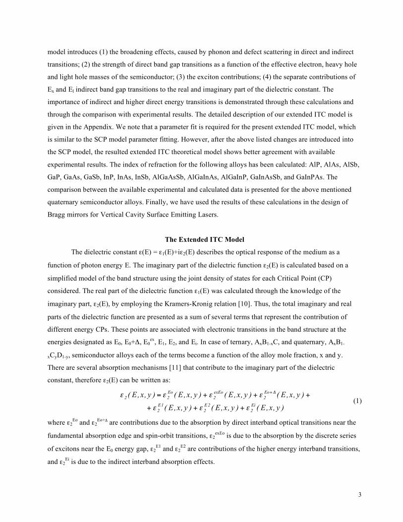
There are several absorption mechanisms [11] that contribute to the imaginary part of the dielectric
constant, therefore ε2(E) can be written as:
)y,x,E()y,x,E()y,x,E(
)y,x,E()y,x,E()y,x,E()y,x,E(
Ei
2
2E
2
1E
2
Eo
2
exEo
2
Eo
22
!!!
!!!! "
+++
+++=+
(1)
where ε2Eo and ε2
Eo+Δ are contributions due to the absorption by direct interband optical transitions near the
fundamental absorption edge and spin-orbit transitions, ε2exEo is due to the absorption by the discrete series
of excitons near the E0 energy gap, ε2E1 and ε2
E2 are contributions of the higher energy interband transitions,
and ε2Ei is due to the indirect interband absorption effects.
4
The absorption spectrum for photon energies greater than the band gap energy is composed of
many peaks correlated with Van-Hove singularities of the joint density of states [11]. For III-V zinc-blende
type semiconductors, the contributions of two main peaks (E1 and E2) must also be included. These peaks
correspond to the direct optical transitions at the L and X points of the BZ, respectively. The E1 peak is
treated as a two dimensional M0 type critical point, while the structure of the E2 peak is characteristic of a
damped harmonic oscillator. The E1 peak arises from the transitions occurring over a large portion of the
BZ around the L critical point (CP), between the upper valence band (VB) and the lowest conduction band
(CB) along the <111> direction in the Brillouin zone. The higher interband transitions in the X region,
along the <100> direction, usually do not correspond to a single well defined critical point (CP). The peak
is assumed as a combination of several transitions resulting in a peak in the joint density of states. These
transitions can occur between the upper VB and the lower components of the second CB around the Γ CP,
between the upper VB and the second lowest CB plus spin-orbit splitting component, between the upper
VB and lower CB along the <100> X direction. Because the investigated model is concerned primarily with
the lower energy transitions, the higher interband transition contributions from the X region were modeled
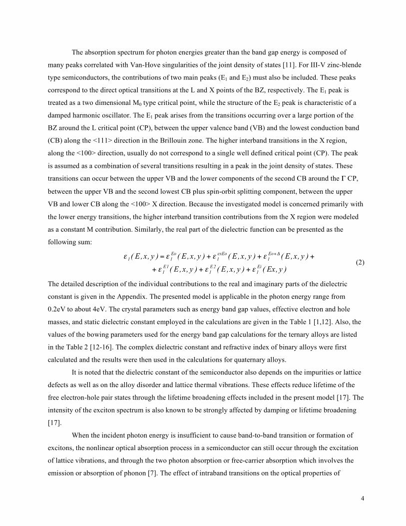
as a constant M contribution. Similarly, the real part of the dielectric function can be presented as the
following sum:
)y,Ex()y,x,E()y,x,E(
)y,x,E()y,x,E()y,x,E()y,x,E(
Ei
1
2E
1
1E
1
Eo
1
exEo
1
Eo
11
!!!
!!!! "
+++
+++=+
(2)
The detailed description of the individual contributions to the real and imaginary parts of the dielectric
constant is given in the Appendix. The presented model is applicable in the photon energy range from
0.2eV to about 4eV. The crystal parameters such as energy band gap values, effective electron and hole
masses, and static dielectric constant employed in the calculations are given in the Table 1 [1,12]. Also, the
values of the bowing parameters used for the energy band gap calculations for the ternary alloys are listed
in the Table 2 [12-16]. The complex dielectric constant and refractive index of binary alloys were first
calculated and the results were then used in the calculations for quaternary alloys.
It is noted that the dielectric constant of the semiconductor also depends on the impurities or lattice
defects as well as on the alloy disorder and lattice thermal vibrations. These effects reduce lifetime of the
free electron-hole pair states through the lifetime broadening effects included in the present model [17]. The
intensity of the exciton spectrum is also known to be strongly affected by damping or lifetime broadening
[17].
When the incident photon energy is insufficient to cause band-to-band transition or formation of
excitons, the nonlinear optical absorption process in a semiconductor can still occur through the excitation
of lattice vibrations, and through the two photon absorption or free-carrier absorption which involves the
emission or absorption of phonon [7]. The effect of intraband transitions on the optical properties of
5
semiconductors is known to be observed at energies well below the fundamental band edge and to become
increasingly pronounced towards longer wavelengths. Their contribution to the refractive index can be
obtained from the classical Drude dispersion theory. Since the present extended ITC model primarily deals
with the transition energies around and above the fundamental absorption edge of the semiconductor under
consideration, the effect of free carrier absorption at very low energies was not included in the calculations.
As a result, the presented model has the lower limit of the applicable energies set at approximately 0.2eV.
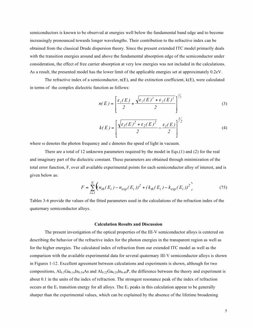
The refractive index of a semiconductor, n(E), and the extinction coefficient, k(E), were calculated
in terms of the complex dielectric function as follows:
21
2
2
2
11
2
)E()E(
2
)E()E(n
!!
"
#
$$
%
& ++=
''' (3)
21
12
22
1
2
)E(
2
)E()E()E(k
!!
"
#
$$
%
&'
+=
((( (4)
where ω denotes the photon frequency and c denotes the speed of light in vacuum.
There are a total of 12 unknown parameters required by the model in Eqs.(1) and (2) for the real
and imaginary part of the dielectric constant. These parameters are obtained through minimization of the
total error function, F, over all available experimental points for each semiconductor alloy of interest, and is
given below as:
( )!=
"+"=N
1i
2iexpith
2iexpith ))E(k)E(k())E(n)E(n(F (75)
Tables 3-6 provide the values of the fitted parameters used in the calculations of the refraction index of the
quaternary semiconductor alloys.
Calculation Results and Discussion
The present investigation of the optical properties of the III-V semiconductor alloys is centered on
describing the behavior of the refractive index for the photon energies in the transparent region as well as
for the higher energies. The calculated index of refraction from our extended ITC model as well as the
comparison with the available experimental data for several quaternary III-V semiconductor alloys is shown
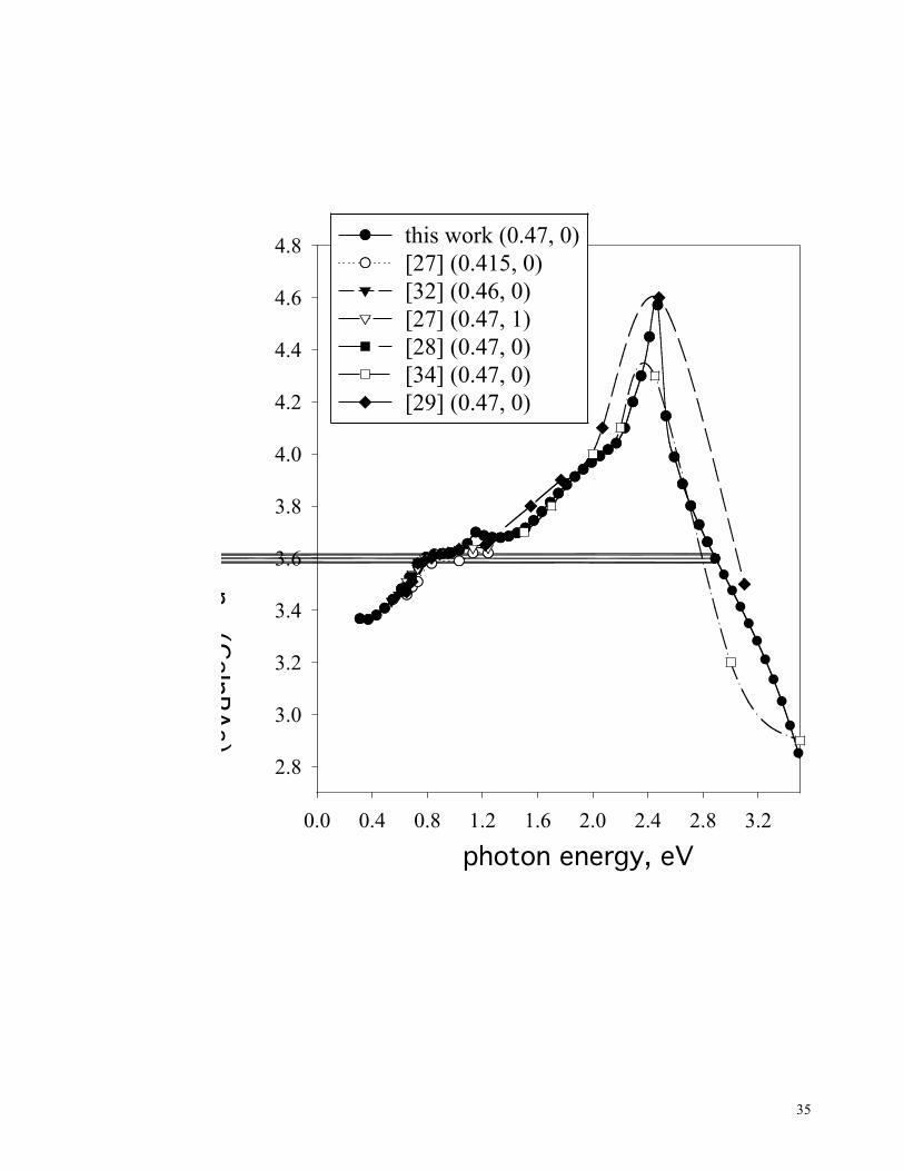
in Figures 1-12. Excellent agreement between calculations and experiments is shown, although for two
compositions, Al0.3Ga0.16In0.54As and Al0.22Ga0.29In0.49P, the difference between the theory and experiment is
about 0.1 in the units of the index of refraction. The strongest resonance peak of the index of refraction
occurs at the E1 transition energy for all alloys. The E1 peaks in this calculation appear to be generally
sharper than the experimental values, which can be explained by the absence of the lifetime broadening
6
effects in the current model for the E1 optical transition. It is believed that by adding the broadening
constant as well as including the exciton effects for the E1 transition energy, better agreement for this peak
can be obtained. The bowing constants of the E0 transition for the quaternary damping parameters were
found positive for all alloys investigated. The increase in the broadening parameter may be attributed to the
potential fluctuations resulting from random atomic placement in the quaternary alloys as compared with
binary alloys. Maximum anion disorder occurs at y=0.5, while that for the cation occurs at x=0.5 and y=1
[18]. Therefore, the high atomic disorder in the triple-cation sublattice of Al0.3Ga0.16In0.54As and
Al0.22Ga0.29In0.49P alloys with compositions x, y, z close to the middle point may be responsible for the
deviations of the calculated refractive index from the one determined experimentally. In this case the
bowing parameters can no longer be represented as a quadratic function of the alloy composition. The
atomic disorder and composition fluctuations are expected to broaden the optical spectra.
The strength parameters of the indirect band gap transitions, described by DL and DX, show a
splitting behavior for most of the alloys. The strength of these transitions is usually divided unequally, with
one of the parameters being higher than the other one. This behavior arises from the unequal contribution of
indirect optical transitions over different regions of the Brillouin zone. Our calculations do not show that
transitions from the L CP prevail as has been assumed in other models [12,19].
The valley contributions to the real part of the dielectric constant are separated according to the
partition of the Brillouin zone. For all materials, the L region with corresponding direct E1 and indirect EL
optical transition energy contributes approximately 65 –75% to the total value of the dielectric constant
while the Γ region corresponding to the E0 transition accounts to about 5-10%, the X region, which is
represented by indirect EX energy and constant M, contributes about 15 to 30% of the total. Thus, the index
of refraction is essentially determined by the band structure away from the center of the BZ, and
modifications of the electronic structure at L and X points rather than Γ CPs, produce the observed
variations in the index of refraction.
The contribution to the total dielectric function of 3D discrete exciton transitions close to the E0
transition energy are found to be negligible, about 0.1%, due to the very narrow spectral range of such
transitions. The continuum exciton transitions at the E0 CP are very similar to noninteracting electron hole
pair characteristics, and therefore their contribution is similar to regular ε(E) expressions at the E0 energy
[20]. Exciton transitions usually are not observed when either the thermal energy exceeds the exciton
binding energy, or when screening effects push the exciton levels into the continuum of CB [21]. Therefore,
room temperature excitonic effects are not as important as those at low temperatures. At low temperatures,
the optical spectra may not be explained within the framework of the one-electron approximation used for
RT model, since the excitonic effects may profoundly modify the CP singularity structure [20].
7
The results of the GaxIn1-xPyAs1-y, AlxGa1-xAsySb1-y, GaxIn1-xAsySb1-y, GaxIn1-xPyAs1-y, AlxGayInzAs
and AlxGayInzP alloys investigation were extrapolated to the different compositions of interest to photonic
devices. In order to select the optimal materials for the semiconductor Distributed Bragg Reflectors (DBRs)
for application in long wavelength Vertical Cavity Surface Emitting Lasers (VCSELs), the maximum and
minimum refractive indices were calculated for response to the incident photon energy of 0.8eV for the
alloys lattice matched to the InP substrate under the direct band gap conditions. The highest index of
refraction difference can be found in GaInAsSb, AlGaInAs, GaInPAs, GaSb, InAs and InSb alloys. The
Al0.05Ga0.42In0.53As/InP material system with index of refraction difference of 0.46 is therefore
recommended for the Bragg mirror applications.
Summary
An extended ITC model and calculations of optical properties for the quaternary III-V
semiconductor alloys are presented and the results are compared with the experimental data. The successful
fit of the refractive indices in the transparent optical region as well as for the higher photon energies was
attained by combining several interband transition contributions. The largest contribution to the dielectric
function for all alloys is due to the direct and indirect optical transitions along <111> and <100> directions
in the BZ, which accounts for 85-90% of the total contributions. Therefore, except for the optical absorption
in the vicinity of the Γ gap, most of the optical properties of the materials, especially the index of refraction,
are determined by the electronic structure around L point, rather than at the center of the BZ. Since our
model is more sensitive to the indirect band gap transitions, the nature of the indirect band gap contributions
to the total dielectric function of the alloy may be better understood. The influence of the discrete exciton
states around the E0 edge at room temperature was found negligible. The strength of the excitonic
transitions is weak and contributes only 0.1% to the dielectric constant. The continuum exciton states at the
E0 and E1 CPs are believed to have a one-electron like characteristics. This ensures that the continuum
exciton contributions to the dielectric constant can be approximated using the expression for the regular E0
or E1 transitions. We have applied the results of these calculations to the AlGaInAs/InP material system for
applications as semiconductor distributed Bragg reflectors.
Acknowledgments
The investigation was funded by the Army Research Laboratory under the Microelectronics Research
Cooperative Agreement, and partially by the University of Maryland Materials Research Science and
Engineering Center.
8
Appendix E0 and E0+Δ Transitions: ε2
E0(E) and ε1E0(E), ε2
E0+Δ(E) and ε1E0+Δ(E) contributions
The direct band gap E0 and the spin-orbit level E0+Δ transitions in the diamond and zinc-blende
type semiconductors occur at the center of the Brillouin zone, at the Γ point. These transitions are the three-
dimensional M0 critical points. The relation between the band structure and ε2(E) is given as:
! ""= ]E)k(E)k(E[)k(MdkmE
e)E( vc
2cv
3
2
22
2 #$
%!
(6)
where the Dirac δ function represents the joint spectral density of states between the valence (VB) and
conduction band (CB) states differing by the energy E=ћω of the incident light, and Mcv(k) is the
momentum matrix element between the VB and CB states. In order to evaluate the contribution of the E0
critical point (CP) to ε2, we considered the momentum matrix element Mcv(k) to be constant with respect to
the photon energy. Therefore, the expression in Eq.(6) for ε2 then becomes:
! ""= ]E)k(E)k(E[dkE
A)E( vc
3
2
Eo2 #$ (7)
where A is the fitting parameter which contains all of the constants and the momentum matrix element The
integral in Eq.(7) is the joint density of states which is proportional to the square root of energy, resulting in
[17]:
)EE(EEE3
A2)E( 002
i2
1i
Eo
2 !!="=
#$ (8)
where i=1 denotes heavy hole and i=2 denotes light hole. The fitting parameters Ai are given by:
!
!!
oo
2
cv
2
5.1
lh
oo
5.1
lh
2
cv
2
2
5.1
hh
oo
5.1
hh
2
cv
2
1
m
Me2 where
u12m12
uMe2A and u
4m4
uMe2A
!"#
#
!"
#
!"
=
====
(9)
where ε0 is a permittivity of vacuum, and m0 is a free electron mass. The reduced effective mass (Eq.(10))
of the electron/heavy hole (light hole), is given as uhh(ulh), where me* is the effective electron mass and
mhh* is the effective heavy hole mass:
*m
1
*m
1
u
1
hhehh
+= (10)
Solving Kramers-Kronig relation for the E0 contribution to ε2, we obtain:
[ ])EE(EEEEE2E
A)E( 00002
i2
1i
Eo1 !!!+!= "
=
#$ (11)
9
where θ(x) is the Heaviside step function,
!"#
<
$=
0x for ,0
0x for ,1)x(% (12)
The model includes two types of interband transition contributions to the dielectric function at the
lowest direct band gap: free electron-hole pair transition (band-to-band transition) and the Wannier exciton
transitions or discrete series excitons. The free exciton transitions in the vicinity of the E0 CP are introduced
through a weakly bounded exciton, having a ground state Rydberg energy given by:
2
o
2
s
2
4
hhex
h8
euR
!!= (13)
where εs is the static dielectric constant.
The ε2ex(E) part of the imaginary dielectric function given in Eq.(14) is due to the E0 ground state
exciton transitions, and may be described by a Lorentzian line shape [20]. The lifetime broadening effects
caused by phonon and defect scattering are included as a complex part of the photon energy E = ћω+iΓ,
where Γ is the half-width at half-maximum (HWHM) of the Lorentzian function for the transitions
investigated. Hence, the following expression is obtained for the imaginary part of the dielectric function
for the E0 transition [9]:
( ) [ ]
( )[ ][ ]
!=
""""
#
$
%%%%
&
'
+(()
)+(+
*+
,-.
/*+,
-./ (
+
+
+=
2
1i
ii0ii
2
o
2
iii
22
o
2
0
0i
ex
i
ex
2
Eo
2
)bsin()aexp(E2)bcos()aexp(1E
)a2exp()bcos()aexp(21E
)EE(tana5.0AR2
)E()E(
00
0
011
22
(14)
where 00
2
cv
22
ex
m2
MeA
!
!= ,
20
20
02
020ex
ii)EE(
EE)EE(R2a
!+
!+!+!=
"
"#
and 2
020
02
020ex
ii)EE(
EE)EE(R2b
!+
+!!+=
"
"#
[ ] [ ] )EE(a3)EE(aE
A)E(
2ex,lh
2exlh
3lh
lhex
2ex,hh
2exhh
3hh
hhex
2exex
2 !!
"
#
$$
%
&
+'+
+'=
(
(
(
(
)* (15)
where Ehhex (Elh
ex ) is the heavy hole (light hole) exciton transition energy given by: E0-Rhhex (E0-Rlh
ex), and
ahh (alh) is the radius (in Å) of the ground state heavy hole (light hole) exciton given as (0.529 εsm0)/uhh. The
HWHM of the Lorentzian line-shape function is given as Γ0 for the E0 transition, and the HWHM of the
10
Lorentzian function for the heavy hole or light hole transitions is given as Γex. To simplify the model, Γhhex
and Γlhex are considered to be equal.
The same broadening and excitonic effects are introduced into the expression of the real part of the
dielectric function from Eqs.(14) and (15), and we obtain:
( )( )[ ])rr(E2)rrE2)(E(
)E2(E
AA
)E()E(
430210
2
0
2
2
0
22
0
2
lhhh
ex
1
Eo
1
+!!!!+!
++
+=
""""
##
(16)
where 2
)EE(EEr
20
200
1
++++=
!
2
)EE(EEr
20
200
2
!++!=
"
2
)EE(EEr
20
200
3
+++!!=
"
2
)EE(EEr
20
200
4
!+++!=
"
and
( )( )
( )( )
E4EEEa3
EE
E4EEEa
EE
A2)E(
2
ex
222
ex
22
lh,ex
ex
lh
3
lh
ex
22
lh,ex
2
ex
222
ex
22
hh,ex
ex
hh
3
hh
ex
22
hh,ex
exex
1
!!!!!!
"
#
$$$$$$
%
&
++'
+'+
+++'
+'
=
((
(
((
(
)* (17)
The contributions from E0+Δ transitions to dielectric function are presented in the simplified form
without broadening effects:
)EE(EEE
A)E( 0002
soEo2 !"!# !
$$$$=+ (18)
and
[ ])EE(EEEEE2E
A)E( 00002
soEo1 !+!+!++!+=+ "#"""$ " (19)
where 5.1
so
oo
5.1
so
2
cv
2
so u6m6
uMe2A
!
"#==
!, and uso denotes the reduced effective mass of electron/hole in the
spin-orbit split-off valence band.
11
E1 Transitions: ε2E1(E) and ε1
E1(E) contributions
The E1 and E1+Δ transitions occur along the <111> direction or at L point in the BZ. The
longitudinal effective mass is much higher than its transverse counterpart, thus, one can treat these CP as
the 2D minimum. Neglecting lifetime broadening effect, the contribution of the E1 transition to ε2(E) is
given as [9]:
( ) )EE()EE(EEBBE
E)E( 1111212
211E
2 !!!!= ""#
$ (20)
where B1 and B2 are the strength parameters of the E1 transition, and E11 is given as
2
2
1111
B
BEE !!
"
#$$%
&'= (21)
From Eqs.(20) and (21), the real part of the dielectric function for E1 transition consists of the two
parts, ε1B1 and ε1
B2, or the contributions from B1 term and B2 term, respectively:
!!
"
#
$$
%
& ''=
211
211
2
2
2111B
1E
|EE|ln
E
EB)E(( (22)
( )
!!!
"
!!!
#
$
%&&
'
(
))
*
+
&&'
())*
+
,
,,,
<&&&
'
(
)))
*
+
&&
'
(
))
*
+
,
,,,,+
=
1
1
11112
2
12
1
11
2
1111
12
2
12
2B
1
EE for EE
EEtanaEEP
E
EB
EE for |EE|
EEEElnEEP
E
EB
)E(- (23)
where ( ) ( )
!!
"
#
$$
%
& '''!!
"
#
$$
%
&
+
''++=
11
2
1111
1
11
2
1111
1
E
EEElnE2
EE
EEEElnEEP
Introducing a broadening effect, Γ1, into the E1 transitions the contribution of the B1 term to ε2(E) is
given by:
( )
( )
( ) ( )!!!!!
"
#
$$$$$
%
&
++!!"
#$$%
& +'+
+!!"
#$$%
&!!"
#$$%
& '''
+=
11
2
1
2
1
2
11
2
1
2
111
1
112
1
2
22
1
2
1
2
11B
2
E
E
E
EElnE
EEtana
2E
E
BE)E(
((((
(
)(
(* (24)
and the contribution of the B2 term to ε2(E) is given by:
12
( )
( )
( )
( )( )
!!!!!!!!!!!!!
"
#
$$$$$$$$$$$$$
%
&
!!!
"
#
$$$
%
&
!!
"
#
$$
%
& ''+
'+'
'
!!!!
"
#
$$$$
%
&
!!
"
#
$$
%
& ''+
++
+
+!"
#$%
&''
+=
=
11
2
1111
111
1112
1
2
1
11
2
1111
1
3241
1
42312
1
2
22
1
2
2
2
1
2B
2
E
EEEln
E
5.0
E
EEE
E
EEElnE2
bb2bb
E
bb2
bbE
E
BE
)E(
((
(
(
(
)
(25)
where b1, b2, b3, and b4 and given by:
( ) ( )
( ) ( ) !!!
"
#
$$$
%
&
+'+''++'''
+'+''++'+'=
2
1
2
11111
2
1
2
1111
2
1
2
11111
2
1
2
1111
1
EEEEEEEE2EE
EEEEEEEE2EElnb
((
((
( )
( )
( )
( ) !!!
"
#
$$$
%
&
+'+'
'++'''+
+!!!
"
#
$$$
%
&
+'+'
'++'+'=
EEEE
EEEEEE2tana
EEEE
EEEEEE2tanab
1
2
1
2
1
1
2
1
2
11
1
2
1
2
1
1
2
1
2
11
2
(
(
(
(
( )2
EEEEb
1
2
1
2
1
3
+!+!=
"
( )2
EEEEb
1
2
1
2
1
4
!++!=
"
The real part of the dielectric constant for the E1 transition with introduced broadening effect is shown in
Eqs.(26) and (27):
13
( )
( )( )
( )
!!!!!!
"
#
$$$$$$
%
&
!!"
#$$%
&!!"
#$$%
& '''
'!!!
"
#
$$$
%
&!"#$
%& +'+
!!
"
#
$$
%
& ++'
(
(+
'=
1
11
1
2
1
2
112
11
2
1
2
112
1
2
22
1
2
2
111B
1
EEtana
2E2
EElnE
EElnE
E
EB)E(
)
*)
))
)
)+
(26)
( )( )
( )
( )
( ) !!!!!!!!!!!!!
"
#
$$$$$$$$$$$$$
%
&
'+
+
!!!!!!!!!!!
"
#
$$$$$$$$$$$
%
&
''
'!!
"
#
$$
%
& '''
'!!
"
#
$$
%
&
+
''++
'
+=
42311
32
41
11
2
1111
1
11
2
1111
1
2
1
2
22
1
2
2
122B
1
bb2bbE
bb2
bb
E
EEElnE2
EE
EEEElnEE
E
E
EB)E(
(
(
() (27)
The total contribution of the real and imaginary part of the dielectric function for the E1 transition is
calculated as a sum of the B1 and B2 terms presented above:
)E()E()E( 2B2
1B2
1E2 !!! += (28)
)E()E()E( 2B1
1B1
1E1 !!! += (29)
E2 and Higher Transitions: ε2E2(E) and ε1
E2(E) contributions
The contributions to the dielectric function from the transitions at energies higher than E1 are
usually labeled as E2 and are modeled as a single damped harmonic oscillator with energy E2 as presented
in Eqs.(30) and (31):
!!!
"
#
$$$
%
&!"#
$%&+!
!"
#$$%
&!"#
$%&'
=2
2
22
22
2E2
EE
EE1E
C)E(
(
() (30)
14
!!!
"
#
$$$
%
&!"#
$%&+!
!"
#$$%
&!"#
$%&'
!!"
#$$%
&!"#
$%&'
=2
2
22
2
2
22E
1
EE
EE1
EE1C
)E(
(
) (31)
where C is the strength parameter of the E2 transition, and β is the damping factor.
Since E2 transitions in X region of the BZ do not correspond to a single, well defined CP, its
characteristics is more complicated for analysis [17]. Higher energy transitions also contribute to the
dielectric function. However, these contributions vary weakly with photon energy. Therefore, we have
modeled the effects of these transitions as a single real additive constant, M, to the real part of the dielectric
function.
Indirect Transitions: ε2Ei(E) and ε1
Ei(E) contributions
Indirect transitions from Γ point states at the VB edge to the X and L point states at the CB edges
are appreciable at room temperature. The transition requires a phonon to conserve both energy and
momentum. The solution for ε2(E) using a second order time-dependent perturbation theory without
introducing a broadening effect is given as [9]:
( ) ( ) ( )EEEEEEE
D)E( cq
idg
2
qidg2
Ei2 !±!±!= "#"#$ !! (32)
where D is the indirect transition strength parameter, and Ec is a cutoff energy which accounts for the finite
width of the energy bands. The phonon energy, ћωq, taking part in the indirect transition was ignored in the
final calculations. The energies of the indirect band gaps at X and L points are always different, and hence
our model treats these transitions separately. Therefore, the dielectric function for the indirect transitions is
presented as a sum of two terms corresponding to EX and EL indirect band gap energies with DX and DL as a
strength parameters of these transitions:
( ) ( ) ( )!=
"#
$%&
'(((=
L
XicL
2i2
iEi2 EEEEEE
E
D)E( ))* (33)
By applying Kramers-Kronig relation to ε2Ei(E) the real part of the dielectric function due to
indirect band gap transitions is obtained [9] and is given in Eq.(34):
( ) ( )!=
""
#
$
%%
&
'
""
#
$
%%
&
'
(
((+""
#
$%%&
'
+
+++""
#
$%%&
'(=
=
L
Xi i
c
2
2
i
i
c
2
2
i
i
c
2
2
ii
Ei
1
EE
EEln
E2
EE
EE
EEln
E2
EE
E
Eln
E
ED2
)E(
)
*
(34)
15
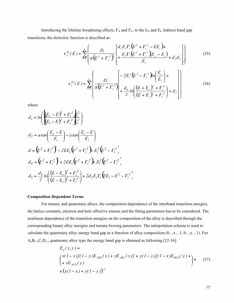
Introducing the lifetime broadening effects, ΓX and ΓL, to the EX and EL indirect band gap
transitions, the dielectric function is described as:
( )
( )( )( )!
= """"
#
$
%%%%
&
'
(((
)
*
+++
,
-
+.+
+
+.+
+=
L
Xi 32
c
ic
2
i
2
ii
i
2
i
2
ii1
22
i
2
iEi
2dd
E
EEEE
EEEEd
E
D)E( //
//
/01 (35)
( )
( )
( )
( )
!=
"""""
#
$
%%%%%
&
'
(((((
)
*
+++++
,
-
+""#
$%%&
'
++
+++
+""#
$%%&
'..
+=
L
Xi
52
i
2
i
2
i
2
c4
i
c2
i
22
i
2
i
2
iEi
1
dEE
EEln
2
d
E
ElnEE2
E
D)E(
/
/
/
/01 (36)
where
( )[ ]( )[ ] !
!
"
#
$$
%
&
+'
+'=
2
c
2
i
2
i
2
i
2
i
2
c1
EEE
EEElnd
(
(
!!"
#$$%
& ''!!"
#$$%
& '=
i
i
i
c2
EEtana
EEtanad
((
( ) ( ) ( )2i22
i
2
i
2
i
22
i
2EEEEE2Ed !!! "++"+=
( ) ( ) ( )2i22
i
2
i
2
i
22
i
2
4 EEEEE2Ed !!! "++++=
( )
( )( )2i2
iii22
i
2
c
2
i
2
c35 EEEEd2
EE
EEln
2
dd !!
!
!""+
##
$
%
&&
'
(
+"
+"=
Composition Dependent Terms
For ternary and quaternary alloys, the composition dependence of the interband transition energies,
the lattice constants, electron and hole effective masses and the fitting parameters has to be considered. The
nonlinear dependence of the transition energies on the composition of the alloy is described through the
corresponding binary alloy energies and ternary bowing parameters. The interpolation scheme is used to
calculate the quaternary alloy energy band gap as a function of alloy composition (0…x…1, 0…y…1). For
AxB1-xCyD1-y quaternary alloy type the energy band gap is obtained as following [12-16]:
( ) 1ACD
BCDABCABD
g
)y1(y)x1(x
)y(xE
)y(E)x1)[(y1(y)]x(yE)x(E)y1)[(x1(x
)y,x(E
!!+!"
"##$
%&&'
(
+
+!!++!!
=
(37)
16
where EABC, EABD, EBCD, and EACD are the ternary alloy energy band gaps containing the corresponding
bowing parameters. For AxByCzD (ABxCyDz ) type quaternary alloys (where 0…x…1, 0…y…1, 0…z…1,
x+y+z=1) the energy band gap is given by Eq.(38) below:
)yx1(x)yx1(yxy
)w(E)yx1(x)v(E)yx1(y)u(xyE)y,x(E ABDACDABC
g!!+!!+
!!+!!+= (38)
where .2
yx22w ;
2
y2x2v ;
2
yx1u
!!=
!!=
+!=
The dependence of the energy band gap of the AxB1-xC ternary alloy on its composition is given as:
)x1(xbpE)x1(xE)x(E ABCBCACg !!!+= (39)
where bpABC is a bowing parameter and, in general is a positive number. The bowing parameters used in the
calculations are given in the Table 2 [12-16].
The composition dependence of the lattice constants, effective electron and hole masses of the
ternary or quaternary alloys is given by the linear Vegard’s law interpolation scheme. Application of the
Vegard’s law based on the linear behavior of the ternary or quaternary parameters allows one to find an
unknown alloy parameter using the available binary alloy or end point constants. Hence, the composition
dependence of A xB1-xC ternary alloy parameter PABC(x) is given as:
BCACABC P)x1(xP)x(P !+= (40)
where PAC and PBC are constant parameter values of the corresponding binary alloys. For the AxB1-xCyD1-y
quaternary alloy type, the parameter PABCD(x,y) is expressed as:
BD
BCADACABCD
P)y1()x1(
Py)x1(P)y1(xPyx)y,x(P
!"!"+
+!!"+!"!+!!= (41)
Likewise, the expression for composition dependence of parameter PABCD(x,y) for AxByCzD ( ABxCyDz )
quaternary alloy type is:
ADACABABCD P)yx1(yPxP)y,x(P !!++= (42)
Each quaternary fitting parameter of the AxB1-xCyD1-y alloy is modeled as a nonlinear function of
the composition z and y, in the following form:
)y1(yBP)x1(xBPP)y1)(x1(
P)y1(xP)x1(yP)x1(x)y,x(P
21BD
ADBCAC
!+!+!!+
+!+!+!= (43)
where PAC, PBC, PAD, PBD are the binary constants corresponding to one of the fitting parameters (α, Γ0, B1,
B2, E1, DX, DL, ΓX, ΓL, Ec, M), BP1 and BP2 are the corresponding bowing parameters. In the case of the
AxByCzD type alloy, the quaternary parameter is given as:
17
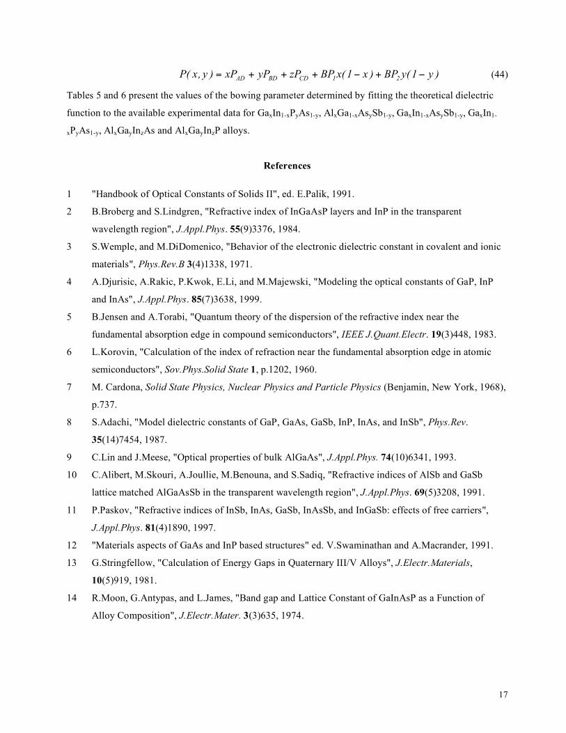
)y1(yBP)x1(xBPzPyPxP)y,x(P 21CDBDAD !+!+++= (44)
Tables 5 and 6 present the values of the bowing parameter determined by fitting the theoretical dielectric
function to the available experimental data for GaxIn1-xPyAs1-y, AlxGa1-xAsySb1-y, GaxIn1-xAsySb1-y, GaxIn1-
xPyAs1-y, AlxGayInzAs and AlxGayInzP alloys.
References 1 "Handbook of Optical Constants of Solids II", ed. E.Palik, 1991.
2 B.Broberg and S.Lindgren, "Refractive index of InGaAsP layers and InP in the transparent
wavelength region", J.Appl.Phys. 55(9)3376, 1984.
3 S.Wemple, and M.DiDomenico, "Behavior of the electronic dielectric constant in covalent and ionic
materials", Phys.Rev.B 3(4)1338, 1971.
4 A.Djurisic, A.Rakic, P.Kwok, E.Li, and M.Majewski, "Modeling the optical constants of GaP, InP
and InAs", J.Appl.Phys. 85(7)3638, 1999.
5 B.Jensen and A.Torabi, "Quantum theory of the dispersion of the refractive index near the
fundamental absorption edge in compound semiconductors", IEEE J.Quant.Electr. 19(3)448, 1983.
6 L.Korovin, "Calculation of the index of refraction near the fundamental absorption edge in atomic
semiconductors", Sov.Phys.Solid State 1, p.1202, 1960.
7 M. Cardona, Solid State Physics, Nuclear Physics and Particle Physics (Benjamin, New York, 1968),
p.737.
8 S.Adachi, "Model dielectric constants of GaP, GaAs, GaSb, InP, InAs, and InSb", Phys.Rev.
35(14)7454, 1987.
9 C.Lin and J.Meese, "Optical properties of bulk AlGaAs", J.Appl.Phys. 74(10)6341, 1993.
10 C.Alibert, M.Skouri, A.Joullie, M.Benouna, and S.Sadiq, "Refractive indices of AlSb and GaSb
lattice matched AlGaAsSb in the transparent wavelength region", J.Appl.Phys. 69(5)3208, 1991.
11 P.Paskov, "Refractive indices of InSb, InAs, GaSb, InAsSb, and InGaSb: effects of free carriers",
J.Appl.Phys. 81(4)1890, 1997.
12 "Materials aspects of GaAs and InP based structures" ed. V.Swaminathan and A.Macrander, 1991.
13 G.Stringfellow, "Calculation of Energy Gaps in Quaternary III/V Alloys", J.Electr.Materials,
10(5)919, 1981.
14 R.Moon, G.Antypas, and L.James, "Band gap and Lattice Constant of GaInAsP as a Function of
Alloy Composition", J.Electr.Mater. 3(3)635, 1974.
18
15 C.Williams, T.Glisson, J.Hauser, and M.Littlejohn, "Energy Band gap and Lattice Constants
Contours of III-V Quaternary Alloys of the Form AxByCzD or ABxCyDz", J.Electr.Materials 7(5)639,
1978.
16 T.Glisson, J.Hauser, M.Littlejohn, and C.Williams, "Energy Band gap and Lattice Constant Contours
of III-V Quaternary Alloys", J.Electr.Mater. 7(1)1, 1978.
17 S.Adachi, "Refractive index of III-V compound: key properties of InGaAsP relevant to device
design", J.Appl.Phys. 53(8)5863, 1982.
18 S.Kelso, D.Aspnes, M.Pollack, and R.Nahory, "Optical properties of InGaAsP from 1.5 to 6.0 eV
determined by spectroscopic ellipsometry", Phys.Rev.B 26(12)6669, 1982.
19 "Semiconductor alloys", by A.Chen and A.Sher, 1995.
20 S.Adachi, "Excitonic effects in the optical spectrum of GaAs", Phys.Rev.B 41(2)1003, 1990.
21 F.Stern, "Dispersion of the index of refraction near the absorption edge of semiconductors",
Phys.Rev. 133(6A)A1653, 1964.
22 D.Jenkins, "Optical constants of AlGaAs", J.Appl.Phys. 68(4)1848, 1990.
23 S.Gehrsitz, F.Reinhart, C.Gourgon, N.Herres, A.Vonlanthen, and H.Sigg, "The refractive index of
AlGaAs below the band gap:accurate determination and empirical modeling", J.Appl.Phys.
87(11)7825, 2000.
24 B.Weigl, M.Grabherr, G.Reiner, and K.Ebeling, "High efficiency selectively oxidized MBE grown
vertical cavity surface emitting lasers", Electrn.Lett. 32(6)557, 1996.
25 Y.Kokubo and I.Ohta, "Refractive index as a function of photon energy for AlGaAs between 1.2 and
1.8eV", J.Appl.Phys. 81(4)2042, 1997.
26 C.Bernardi, M.Meliga, S.Morasca, C.Rigo, B.Sordo, and A.Stano, "Refractive indices of InGaAlAs
grown by MBE", J.Appl.Phys. 68(12)6513, 1990.
27 H.Dinges, H.Burkhard, R.Nickel, and W.Schlapp, "Spectroscopic ellipsometry: a useul tool to
determine the refractive indices and interfaces of InAlAs and InAlGaAs layers on InP in the
wavelength range 280-1900nm", Mater.Sci.Engin.B 21, p.174, 1993.
28 M.Mondry, D.Babic, J.Bowers, and L.Coldren, "Refractive indices of (AlGaIn)As epilayers on InP
for optoelectronic applications", IEEE Pton.Techn.Lett. 4(6)627, 1992.
29 H.Dinges, H.Burkhard, R.Losch, H.Nickel, and W.Schlapp, "Refractive indices of InAlAs and
InGaAs/InP from 250 to 1900nm determined by spectroscopic ellipsometry", Appl.Surf.Sci. 54,
p.477, 1992.
30 H.Tanaka, Y.Kawamura, and H.Asahi, "Refractive indices of InGaAlP lattice matched to GaAs",
J.Appl.Phys. 59(3)984, 1986.
19
31 Y.Kaneko and K.Kishino, "Refractive indices measurement of (GaInP)(AlInP) quasi-quaternaries and
GaInP/AlInP multiple quantum wells", J.Appl.Phys. 76(3)1809, 1994.
32 P.Chandra, L.Coldren, and K.Strege, "Refractive index data from GaInAsP films", Electrn.Lett.
17(1)6, 1981.
33 "Semiconductors - Basic data", ed. O.Madelung, 1996.
34 C.Pickering, N.Garawal, D.Lacefield, J.Piel, and R.Blunt, "Non-destructive characterization of
(GaInAlAsP)-based ternary multilayer structures using spectroscopic ellipsometry", Appl.Surf.Sci. 50,
p.346, 1991.
35 M.Munoz, K.Wei, F.Pollak, J.Freeouf, C.Wang, and G.Charache, "Optical constants of GaInAsAb
lattice matched to GaSb(001): experiment and modeling", J.Appl.Phys. 87(4)1780, 2000.
20
Figure Captions
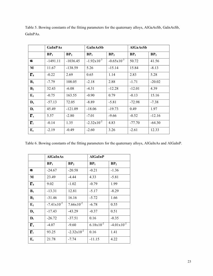
Figure 1. Refractive index of AlxGa1-xAsySb1-y for x=0.8, y=1.
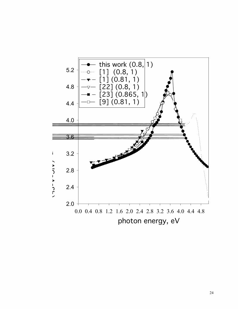
Figure 2. Refractive index of AlxGa1-xAsySb1-y for x=0.4, y=1.
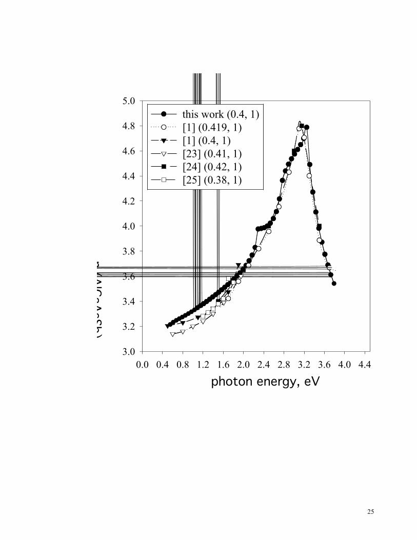
Figure 3. Refractive index of AlxGa1-xAsySb1-y for x=0.2, y=1.
Figure 4. Refractive index of AlxGayInzAs for x=0.3, y=0.16, z=0.54.
Figure 5. Refractive index of AlxGayInzAs for x=0.48, y=0, z=0.52.
Figure 6. Refractive index of AlxGayInzAs for x=0, y=0.47, z=0.53.
Figure 7. Refractive index of AlxGayInzP for x=0.5, y=0, z=0.5.
Figure 8. Refractive index of AlxGayInzP for x=0.22, y=0.29, z=0.49.
Figure 9. Refractive index of GaxIn1-xAsySb1-y for x=0.85, y=0.14.
Figure 10. Refractive index of GaxIn1-xAsySb1-y for x=0.47, y=1.
Figure 11. Refractive index of GaxIn1-xPyAs1-y for x=0.24, y=0.49.
Figure 12. Refractive index of GaxIn1-xPyAs1-y for x=0.47, y=0.
21
Tables
Table 1. Material parameters of the binary III-V semiconductor alloys used in the calculations [1,12].
AlP AlAs AlSb GaP GaAs GaSb InP InAs InSb
a, Å 5.464 5.661 6.136 5.451 5.653 6.096 5.869 6.058 6.479
E0, eV 3.62 3.03 2.3 2.78 1.424 0.75 1.344 0.354 0.172
EX, eV 2.41 2.153 1.615 2.272 1.804 1.25 2.74 2.28 1.71
EL, eV 4.0 2.363 2.211 2.637 1.81 0.81 1.74 1.53 1.03
Δ , eV 0.0 0.3 0.673 0.08 0.341 0.819 0.07 0.38 0.85
Me lngeff 3.67 1.1 1.64 7.25 0.063 0.041 0.077 0.022 0.014
Me treff 0.212 0.19 0.23 0.313 - - - - -
Mhheff 0.513 0.409 0.94 0.56 0.5 0.28 0.56 0.35 0.34
Mlheff 0.211 0.153 0.14 0.16 0.076 0.05 0.12 0.026 0.016
ε s 9.8 10.06 12.04 11.11 12.9 15.7 12.61 12.25 17.76
Table 2. Bowing parameters of the ternary semiconductor alloys used for the calculations of the energy
band gap values [12-16].
C0, eV CX, eV CL, eV C0, eV CX, eV CL, eV
AlPSb 1.2 0.0 0.0 AlGaP 0.0 0.0 0.0
AlPAs 0.22 0.0 0.0 AlInP 0.0 0.0 0.0
AlAsSb 0.72 0.0 0.0 GaInP 0.758 0.15 0.68
GaPSb 1.2 0.0 0.0 AlGaAs 0.438 0.16 0.0
GaPAs 0.186 0.211 0.25 AlInAs 0.74 0.0 0.0
GaAsSb 1.2 1.09 0.09 GaInAs 0.4 0.15 0.5
InPSb 1.2 1.56 1.6 AlGaSb 0.47 0.0 0.21
InPAs 0.36 0.27 0.26 AlInSb 0.42 0.0 0.0
InAsSb 0.596 0.6 0.55 GaInSb 0.413 0.24 0.33
22
Table 3. Values of the fitted parameters obtained from the index of refraction simulations for the binary III-
V semiconductor alloys, AlP, AlAs, AlSb, GaP, GaAs, GaSb.
AlP AlAs AlSb GaP GaAs GaSb
α 499.99 281.4 59.62 111.44 1238.17 5137.22
M 0.602 -2.247 1.499 1.116 2.087 25.04
Γ0 0.01 0.001 0.001 0.01 0.0161 0.01
B1 1.883 6.416 3.759 5.452 4.624 5.328
B2 9.973 12.25 7.126 11.549 7.724 9.491
E1 4.2 3.886 2.809 3.63 2.906 2.02
Dx 2.166 0.0 16.93 -13.48 13.81 -27.59
Dl 0.0 11.29 60.81 -5.581 5.03 9.548
Γx 0.01 0.001 0.001 0.01 0.001 -2.0
Γ l 0.01 0.001 0.001 0.01 0.001 0.7783
Ec 6.01 8.077 4.268 3.238 5.771 35.1
Table 4. Values of the fitted parameters obtained from the index of refraction simulations for the binary III-
V semiconductor alloys, InP, InAs, InSb.
InP InAs InSb
α 873.09 4035.03 1289.11
M 3.163 6.91 3.298
Γ0 0.01 0.28 0.0001
B1 4.586 2.062 1.529
B2 6.913 5.262 4.429
E1 3.1 2.45 1.81
Dx -42.51 -10.0 -42.88
Dl 14.077 48.31 51.89
Γx 0.01 0.01 0.01
Γ l 0.01 0.01 0.01
Ec 3.325 3.145 3.907
23
Table 5. Bowing constants of the fitting parameters for the quaternary alloys, AlGaAsSb, GaInAsSb,
GaInPAs.
GaInPAs GaInAsSb AlGaAsSb
BP1 BP2 BP1 BP2 BP1 BP2
α -1491.11 -1036.45 -1.92x10⁻³ -0.65x10⁻³ 50.72 41.56
M 11.67 -138.59 5.26 -15.14 15.84 -8.13
Γ0 -0.22 2.69 0.65 1.14 2.83 5.28
B1 -7.79 108.05 -2.18 2.88 -1.71 -20.02
B2 32.43 -6.08 -4.31 -12.28 -12.01 4.39
E1 -0.75 163.55 -0.90 0.79 -0.13 15.16
Dx -57.13 72.05 -8.89 -5.81 -72.98 -7.38
Dl 45.49 -121.09 -18.06 -19.73 0.49 1.97
Γx 5.57 -2.80 -7.01 -9.66 -0.52 -12.16
Γ l -0.14 1.35 -2.32x10⁻² 4.83 -77.70 -64.30
Ec -2.19 -0.49 -2.60 3.26 -2.61 12.33
Table 6. Bowing constants of the fitting parameters for the quaternary alloys, AlGaInAs and AlGaInP.
AlGaInAs AlGaInP
BP1 BP2 BP1 BP2
α -24.67 -20.58 -0.21 -1.36
M 23.49 -4.44 4.33 -5.81
Γ0 9.02 -1.02 -0.79 1.99
B1 -13.31 12.81 -5.17 -8.29
B2 -31.46 16.16 -5.72 1.66
E1 -7.41x10⁻³ 7.66x10⁻² -6.78 0.55
Dx -17.43 -43.29 -0.37 0.51
Dl -26.72 -37.51 0.16 -0.35
Γx -4.07 -9.60 6.18x10⁻² -4.01x10⁻²
Γ l 93.25 -2.32x10⁻² 0.16 1.41
Ec 21.78 -7.74 -11.15 4.22
24
photon energy, eV
0.0 0.4 0.8 1.2 1.6 2.0 2.4 2.8 3.2 3.6 4.0 4.4 4.8
n (A
lGaA
sSb)
2.0
2.4
2.8
3.2
3.6
4.0
4.4
4.8
5.2
this work (0.8, 1)[1] (0.8, 1)[1] (0.81, 1)[22] (0.8, 1)[23] (0.865, 1)[9] (0.81, 1)
25
photon energy, eV
0.0 0.4 0.8 1.2 1.6 2.0 2.4 2.8 3.2 3.6 4.0 4.4
n (A
lGaA
sSb)
3.0
3.2
3.4
3.6
3.8
4.0
4.2
4.4
4.6
4.8
5.0
this work (0.4, 1)
[1] (0.419, 1)
[1] (0.4, 1)
[23] (0.41, 1)
[24] (0.42, 1)
[25] (0.38, 1)
26
photon energy, eV
0.0 0.4 0.8 1.2 1.6 2.0 2.4 2.8 3.2 3.6 4.0
n (A
lGaA
sSb)
2.8
3.0
3.2
3.4
3.6
3.8
4.0
4.2
4.4
4.6
4.8
5.0
5.2
this work (0.2, 1)
[1] (0.198, 1)
[1] (0.2, 1)
[4] (0.2, 1)
[25] (0.2, 1)
27
photon energy, eV
0.0 0.4 0.8 1.2 1.6 2.0 2.4 2.8 3.2
n (A
lGaIn
As)
3.0
3.2
3.4
3.6
3.8
4.0
4.2
4.4
4.6
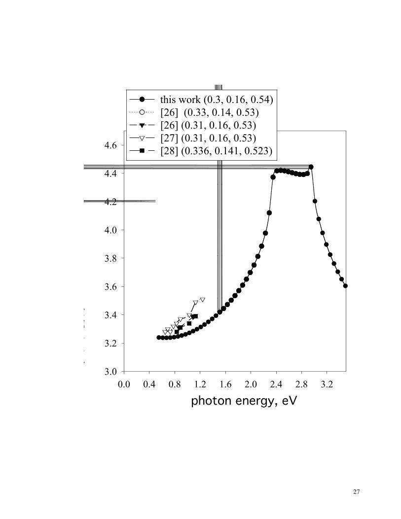
this work (0.3, 0.16, 0.54)
[26] (0.33, 0.14, 0.53)
[26] (0.31, 0.16, 0.53)
[27] (0.31, 0.16, 0.53)
[28] (0.336, 0.141, 0.523)
28
photon energy, eV
0.0 0.4 0.8 1.2 1.6 2.0 2.4 2.8 3.2 3.6 4.0
n (A
lGaIn
As)
3.0
3.2
3.4
3.6
3.8
4.0
4.2
4.4
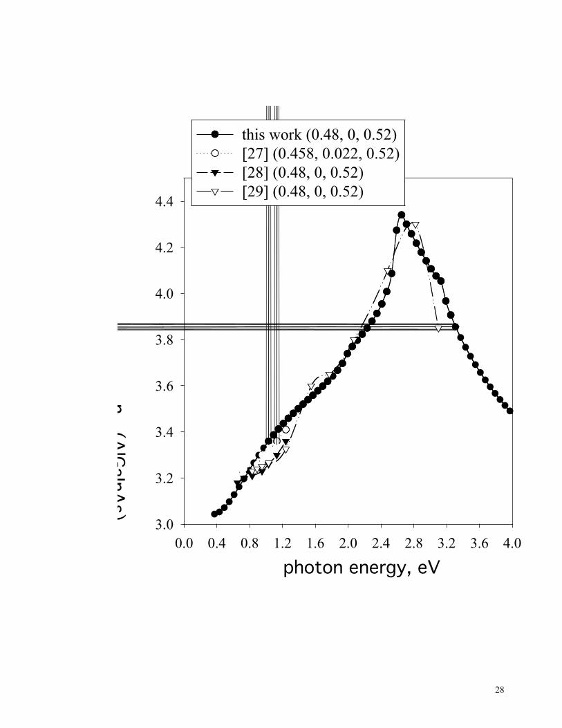
this work (0.48, 0, 0.52)
[27] (0.458, 0.022, 0.52)
[28] (0.48, 0, 0.52)
[29] (0.48, 0, 0.52)
29
photon energy, eV
0.4 0.8 1.2 1.6 2.0 2.4 2.8 3.2 3.6 4.0
n (A
lGaIn
As) 2.4
2.8
3.2
3.6
4.0
4.4
4.8
5.2
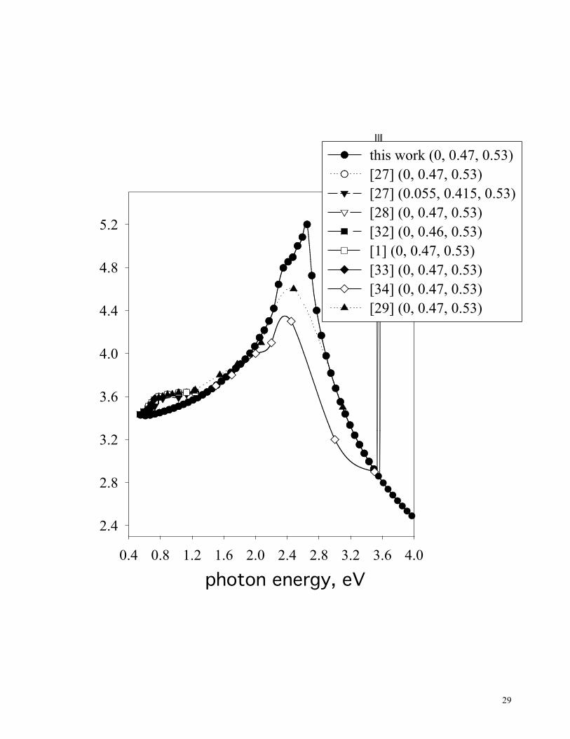
this work (0, 0.47, 0.53)
[27] (0, 0.47, 0.53)
[27] (0.055, 0.415, 0.53)
[28] (0, 0.47, 0.53)
[32] (0, 0.46, 0.53)
[1] (0, 0.47, 0.53)
[33] (0, 0.47, 0.53)
[34] (0, 0.47, 0.53)
[29] (0, 0.47, 0.53)
30
photon energy, eV
0.0 0.4 0.8 1.2 1.6 2.0 2.4 2.8 3.2 3.6 4.0
n (A
lGaIn
P)
2.6
2.8
3.0
3.2
3.4
3.6
3.8
4.0
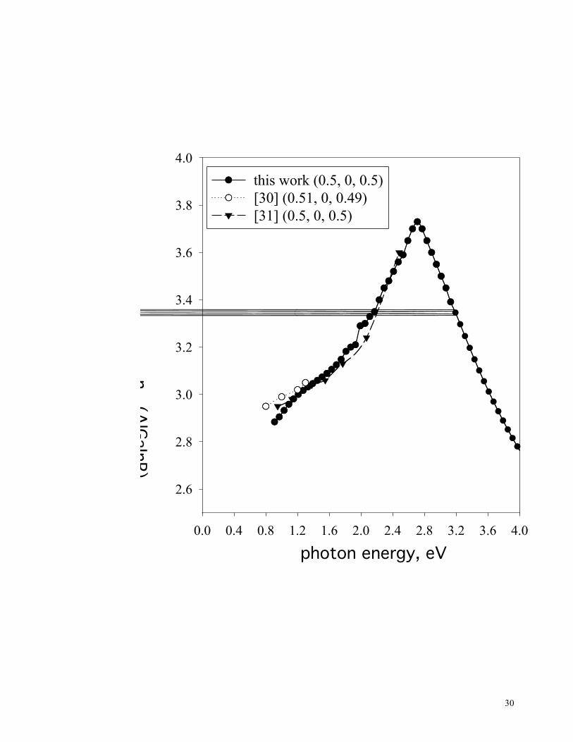
this work (0.5, 0, 0.5)
[30] (0.51, 0, 0.49)
[31] (0.5, 0, 0.5)
31
photon energy, eV
0.0 0.4 0.8 1.2 1.6 2.0 2.4 2.8 3.2 3.6 4.0
n (A
lGaIn
P)
2.6
2.8
3.0
3.2
3.4
3.6
3.8
4.0
4.2
4.4
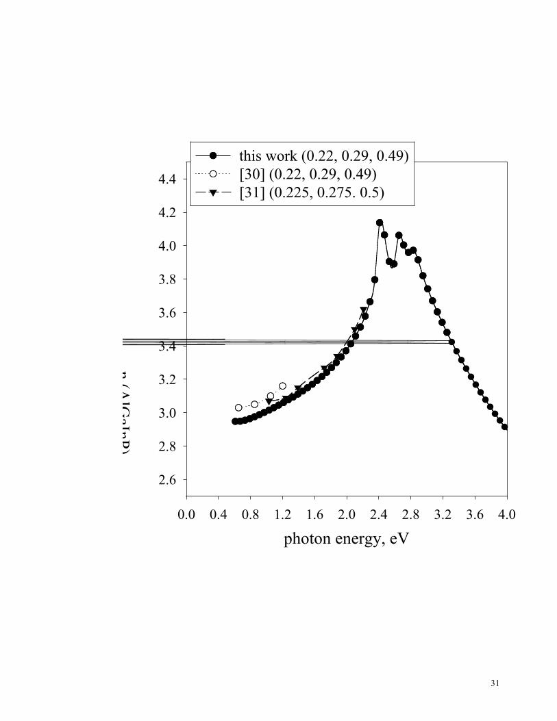
this work (0.22, 0.29, 0.49)
[30] (0.22, 0.29, 0.49)
[31] (0.225, 0.275. 0.5)
32
photon energy, eV
0.0 0.4 0.8 1.2 1.6 2.0 2.4 2.8 3.2
n (G
aIn
AsS
b) 3.6
3.8
4.0
4.2
4.4
4.6
4.8
5.0
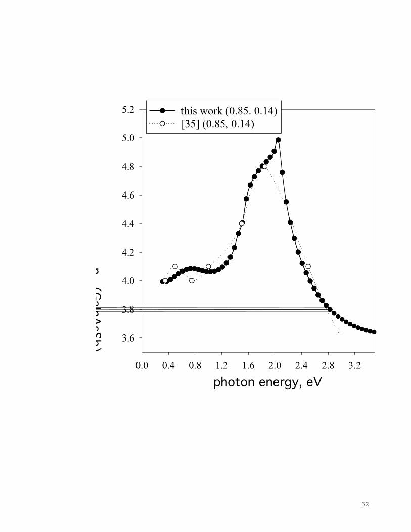
5.2 this work (0.85. 0.14)
[35] (0.85, 0.14)
33
photon energy, eV
0.0 0.4 0.8 1.2 1.6 2.0 2.4 2.8 3.2 3.6
n (G
aInA
sSb)
2.8
3.0
3.2
3.4
3.6
3.8
4.0
4.2
4.4
4.6
4.8
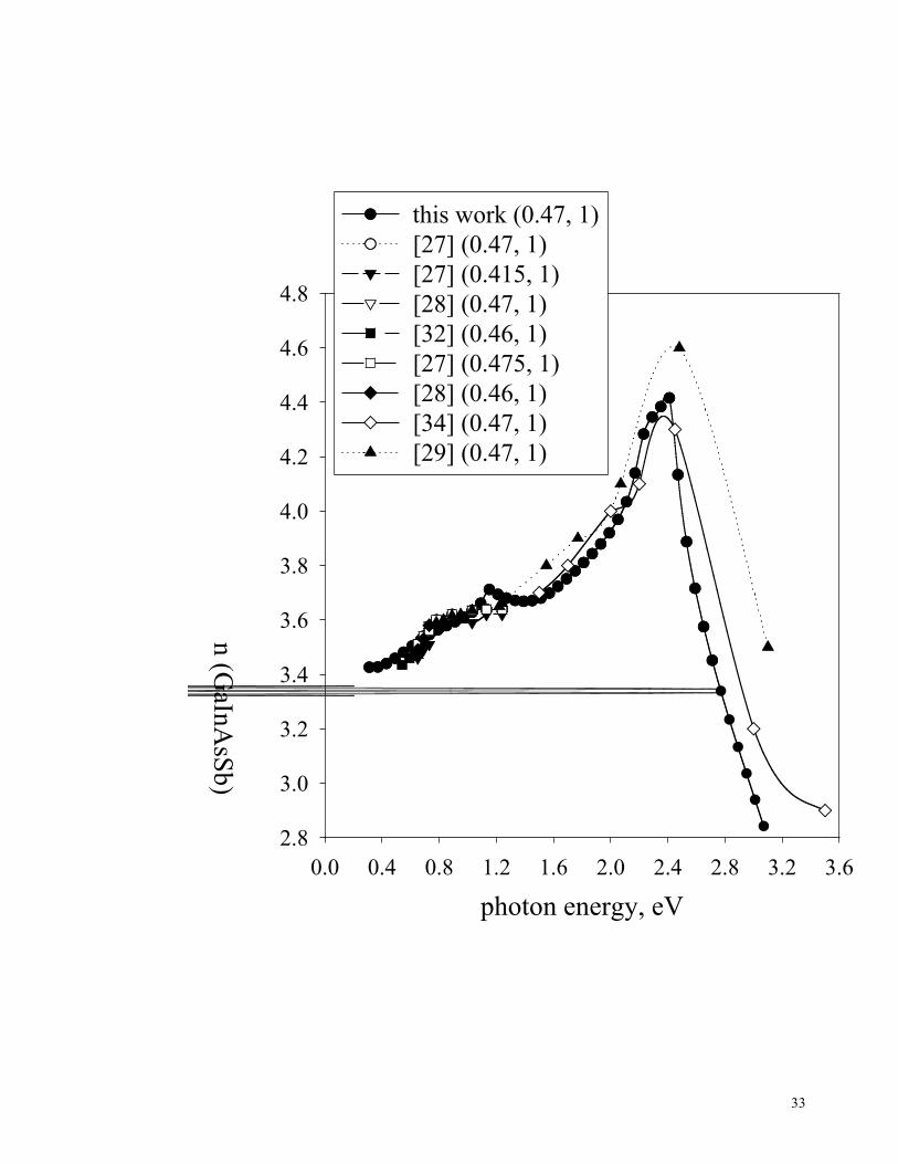
this work (0.47, 1)
[27] (0.47, 1)
[27] (0.415, 1)
[28] (0.47, 1)
[32] (0.46, 1)
[27] (0.475, 1)
[28] (0.46, 1)
[34] (0.47, 1)
[29] (0.47, 1)
34
photon energy, eV
0.0 0.2 0.4 0.6 0.8 1.0 1.2 1.4 1.6 1.8 2.0 2.2 2.4
n (G
aIn
PA
s)
2.8
3.0
3.2
3.4
3.6
3.8
4.0
4.2
4.4
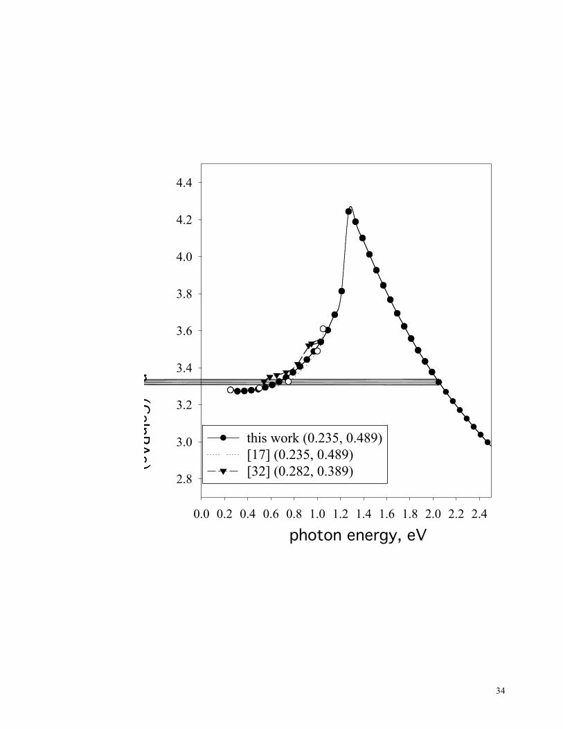
this work (0.235, 0.489)
[17] (0.235, 0.489)
[32] (0.282, 0.389)
35
photon energy, eV
0.0 0.4 0.8 1.2 1.6 2.0 2.4 2.8 3.2
n (G
aIn
PA
s)
2.8
3.0
3.2
3.4
3.6
3.8
4.0
4.2
4.4
4.6
4.8this work (0.47, 0)
[27] (0.415, 0)
[32] (0.46, 0)
[27] (0.47, 1)
[28] (0.47, 0)
[34] (0.47, 0)
[29] (0.47, 0)