Embed Size (px)
Citation preview
1
Cadence Tutorial Introduction to Cadence 0.18um, Implementation and Simulation of an
inverter A. Moradi, A. Miled et M. Sawan
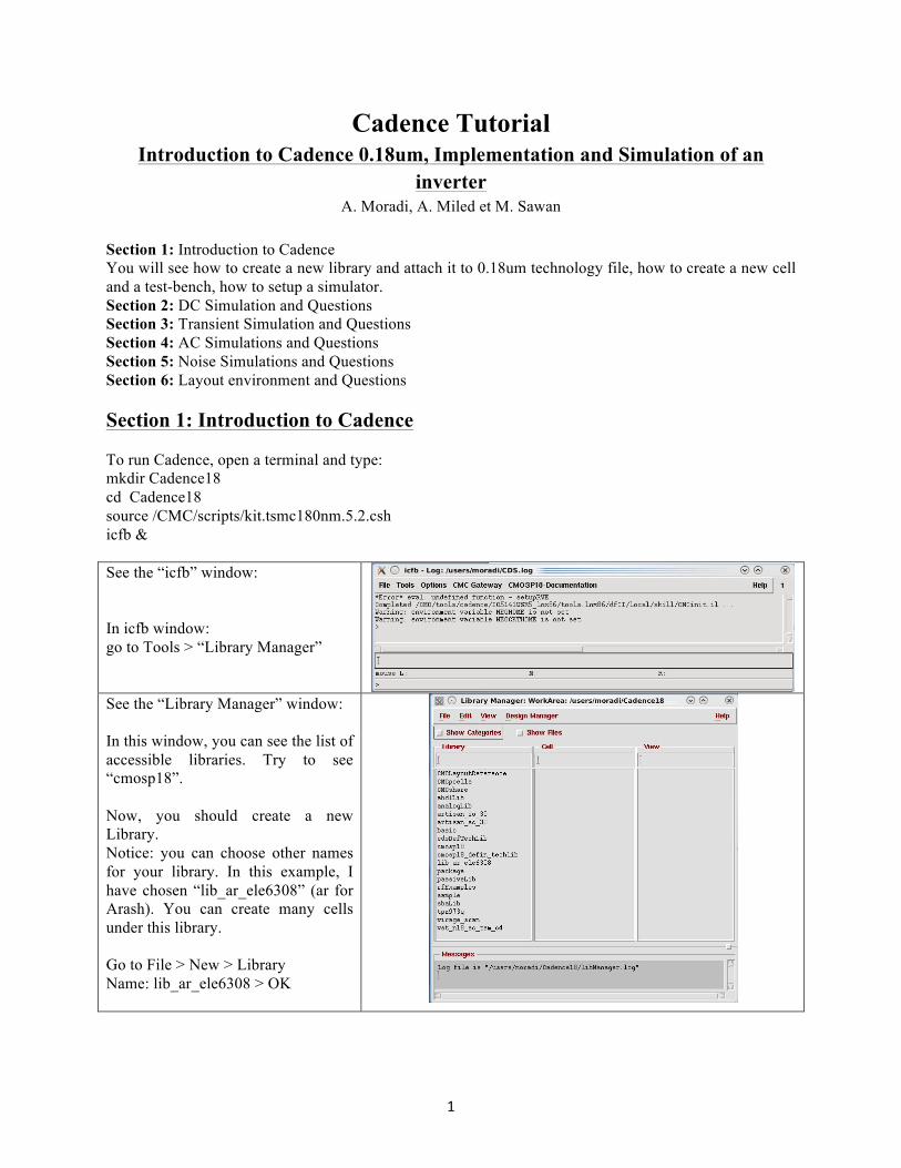
Section 1: Introduction to Cadence You will see how to create a new library and attach it to 0.18um technology file, how to create a new cell and a test-bench, how to setup a simulator. Section 2: DC Simulation and Questions Section 3: Transient Simulation and Questions Section 4: AC Simulations and Questions Section 5: Noise Simulations and Questions Section 6: Layout environment and Questions Section 1: Introduction to Cadence To run Cadence, open a terminal and type: mkdir Cadence18 cd Cadence18 source /CMC/scripts/kit.tsmc180nm.5.2.csh icfb & See the “icfb” window: In icfb window: go to Tools > “Library Manager”
See the “Library Manager” window: In this window, you can see the list of accessible libraries. Try to see “cmosp18”. Now, you should create a new Library. Notice: you can choose other names for your library. In this example, I have chosen “lib_ar_ele6308” (ar for Arash). You can create many cells under this library. Go to File > New > Library Name: lib_ar_ele6308 > OK
GBM8320- Smart Medical Devices Winter 2013
2
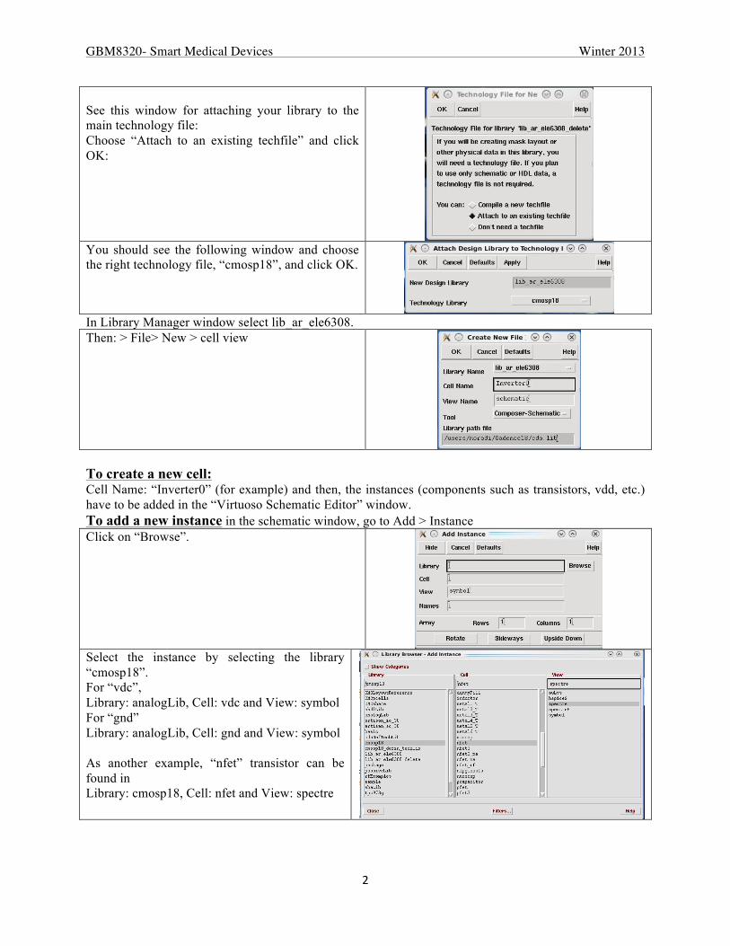
See this window for attaching your library to the main technology file: Choose “Attach to an existing techfile” and click OK:
You should see the following window and choose the right technology file, “cmosp18”, and click OK.
In Library Manager window select lib_ar_ele6308. Then: > File> New > cell view
To create a new cell: Cell Name: “Inverter0” (for example) and then, the instances (components such as transistors, vdd, etc.) have to be added in the “Virtuoso Schematic Editor” window. To add a new instance in the schematic window, go to Add > Instance Click on “Browse”.
Select the instance by selecting the library “cmosp18”. For “vdc”, Library: analogLib, Cell: vdc and View: symbol For “gnd” Library: analogLib, Cell: gnd and View: symbol As another example, “nfet” transistor can be found in Library: cmosp18, Cell: nfet and View: spectre
GBM8320- Smart Medical Devices Winter 2013
3
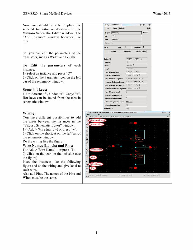
Now you should be able to place the selected transistor or dc-source in the Virtuoso Schematic Editor window. The “Add Instance” window becomes like this: So, you can edit the parameters of the transistors, such as Width and Length. To Edit the parameters of each instance: 1) Select an instance and press “Q” 2) Click on the Parameter icon on the left bar of the schematic window. Some hot keys: Fit to Screen: “f”, Undo: “u”, Copy: “c”. Hot keys can be found from the tabs in schematic window.
Wiring: You have different possibilities to add the wires between the instances in the “Vituoso Schematic Editor” window. 1) >Add > Wire (narrow) or press “w”. 2) Click on the shortcut on the left bar of the schematic window. Do the wiring like the figure. Wire Names (Labels) and Pins: 1) >Add > Wire Name… or press “l”. 2) Click on the icon on the left side (see the figure) Place the instances like the following figure and do the wiring and give label to each wire. Also add Pins. The names of the Pins and Wires must be the same.
GBM8320- Smart Medical Devices Winter 2013
4
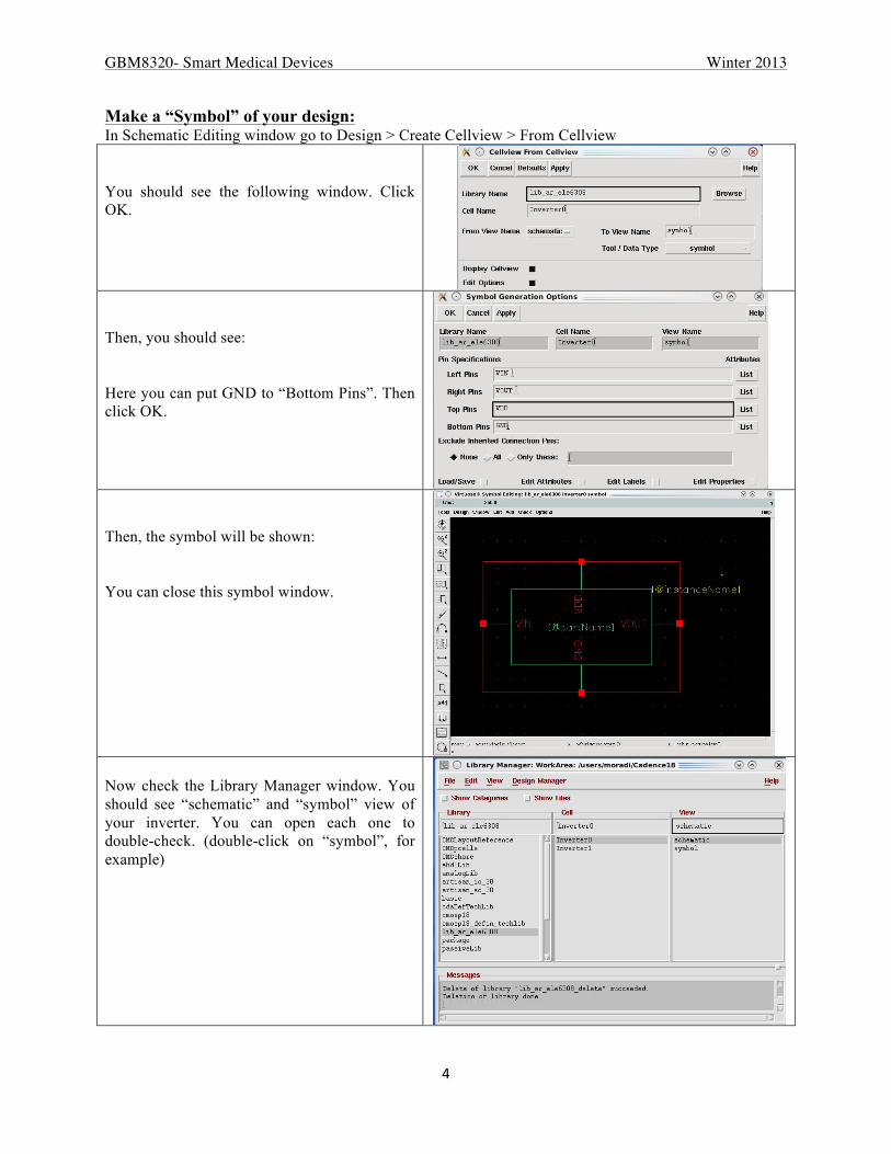
Make a “Symbol” of your design: In Schematic Editing window go to Design > Create Cellview > From Cellview You should see the following window. Click OK.
Then, you should see: Here you can put GND to “Bottom Pins”. Then click OK.
Then, the symbol will be shown: You can close this symbol window.
Now check the Library Manager window. You should see “schematic” and “symbol” view of your inverter. You can open each one to double-check. (double-click on “symbol”, for example)
GBM8320- Smart Medical Devices Winter 2013
5
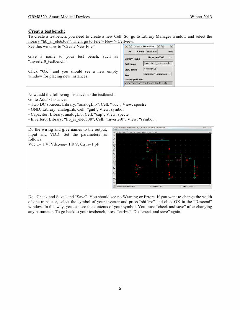
Creat a testbench: To create a testbench, you need to create a new Cell. So, go to Library Manager window and select the library “lib_ar_ele6308”. Then, go to File > New > Cellview. See this window to “Create New File”. Give a name to your test bench, such as “Inverter0_testbench”. Click “OK” and you should see a new empty window for placing new instances.
Now, add the following instances to the testbench. Go to Add > Instances - Two DC sources: Library: “analogLib”, Cell: “vdc”, View: spectre - GND: Library: analogLib, Cell: “gnd”, View: symbol - Capacitor: Library: analogLib, Cell: “cap”, View: specte - Inverter0: Library: “lib_ar_ele6308”, Cell: “Inverter0”, View: “symbol”. Do the wiring and give names to the output, input and VDD. Set the parameters as follows: Vdc,in= 1 V, Vdc,VDD= 1.8 V, C,load=1 pF
Do “Check and Save” and “Save”. You should see no Warning or Errors. If you want to change the width of one transistor, select the symbol of your inverter and press “shift+e” and click OK in the “Descend” window. In this way, you can see the contents of your symbol. You must “check and save” after changing any parameter. To go back to your testbench, press “ctrl+e”. Do “check and save” again.
GBM8320- Smart Medical Devices Winter 2013
6
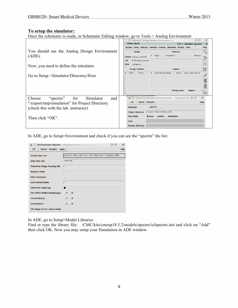
To setup the simulator: Once the schematic is ready, in Schematic Editing window, go to Tools > Analog Environment You should see the Analog Design Environment (ADE). Now, you need to define the simulator. Go to Setup >Simulator/Directory/Host
Choose “spectre” for Simulator and “/export/tmp/simulation” for Project Directory. (check this with the lab. instructor) Then click “OK”.
In ADE, go to Setup>Environment and check if you can see the “spectre” the list:
In ADE, go to Setup>Model Libraries Find or type the library file: /CMC/kits/cmosp18.5.2/models/spectre/icfspectre.init and click on “Add” then click OK. Now you may setup your Simulation in ADE window.
GBM8320- Smart Medical Devices Winter 2013
7
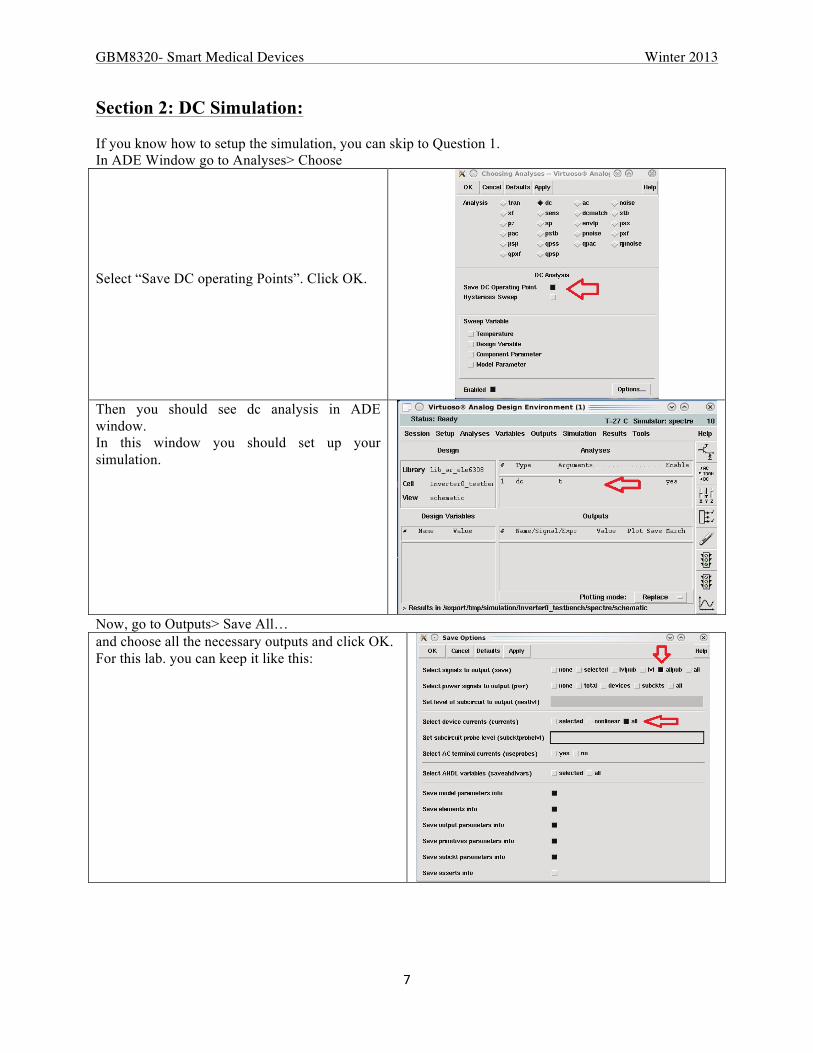
Section 2: DC Simulation: If you know how to setup the simulation, you can skip to Question 1. In ADE Window go to Analyses> Choose Select “Save DC operating Points”. Click OK.
Then you should see dc analysis in ADE window. In this window you should set up your simulation.
Now, go to Outputs> Save All… and choose all the necessary outputs and click OK. For this lab. you can keep it like this:
GBM8320- Smart Medical Devices Winter 2013
8
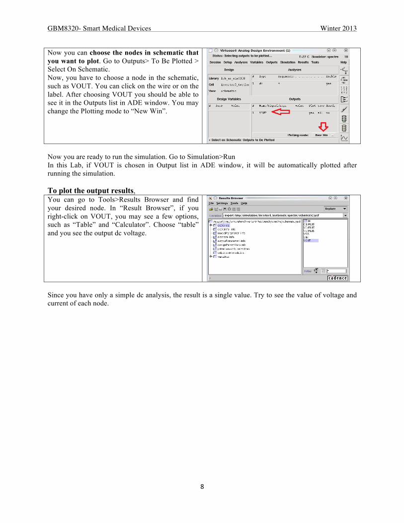
Now you can choose the nodes in schematic that you want to plot. Go to Outputs> To Be Plotted > Select On Schematic. Now, you have to choose a node in the schematic, such as VOUT. You can click on the wire or on the label. After choosing VOUT you should be able to see it in the Outputs list in ADE window. You may change the Plotting mode to “New Win”.
Now you are ready to run the simulation. Go to Simulation>Run In this Lab, if VOUT is chosen in Output list in ADE window, it will be automatically plotted after running the simulation. To plot the output results, You can go to Tools>Results Browser and find your desired node. In “Result Browser”, if you right-click on VOUT, you may see a few options, such as “Table” and “Calculator”. Choose “table” and you see the output dc voltage.
Since you have only a simple dc analysis, the result is a single value. Try to see the value of voltage and current of each node.
GBM8320- Smart Medical Devices Winter 2013
9
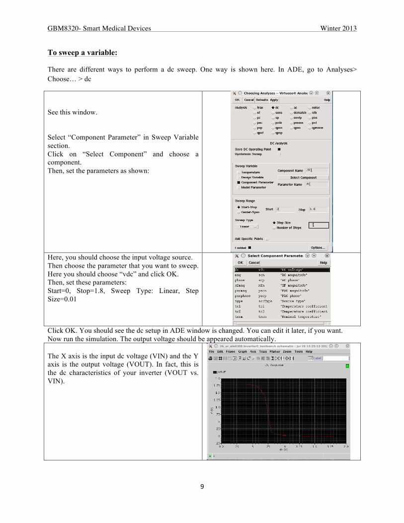
To sweep a variable:
There are different ways to perform a dc sweep. One way is shown here. In ADE, go to Analyses> Choose… > dc
See this window. Select “Component Parameter” in Sweep Variable section. Click on “Select Component” and choose a component. Then, set the parameters as shown:
Here, you should choose the input voltage source. Then choose the parameter that you want to sweep. Here you should choose “vdc” and click OK. Then, set these parameters: Start=0, Stop=1.8, Sweep Type: Linear, Step Size=0.01
Click OK. You should see the dc setup in ADE window is changed. You can edit it later, if you want. Now run the simulation. The output voltage should be appeared automatically. The X axis is the input dc voltage (VIN) and the Y axis is the output voltage (VOUT). In fact, this is the dc characteristics of your inverter (VOUT vs. VIN).
GBM8320- Smart Medical Devices Winter 2013
10
Setting a Variable and Parametric Analysis:
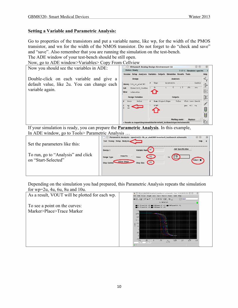
Go to properties of the transistors and put a variable name, like wp, for the width of the PMOS transistor, and wn for the width of the NMOS transistor. Do not forget to do “check and save” and “save”. Also remember that you are running the simulation on the test-bench. The ADE window of your test-bench should be still open. Now, go to ADE window>Variables> Copy From Cellview Now you should see the variables in ADE: Double-click on each variable and give a default value, like 2u. You can change each variable again.
If your simulation is ready, you can prepare the Parametric Analysis. In this example, In ADE window, go to Tools> Parametric Analysis … Set the parameters like this: To run, go to “Analysis” and click on “Start-Selected”
Depending on the simulation you had prepared, this Parametric Analysis repeats the simulation for wp=2u, 4u, 6u, 8u and 10u. As a result, VOUT will be plotted for each wp. To see a point on the curves: Marker>Place>Trace Marker
GBM8320- Smart Medical Devices Winter 2013
11
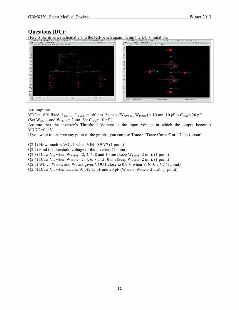
Questions (DC): Here is the inverter schematic and the test-bench again. Setup the DC simulation.
Assumption: VDD=1.8 V fixed. LNMOS , LPMOS = 180 nm. 2 um < (WNMOS , WPMOS) < 10 um, 10 pF < Cload < 20 pF (Set WNMOS and WPMOS= 2 um. Set Cload= 10 pF.) Assume that the inverter’s Threshold Voltage is the input voltage at which the output becomes VDD/2=0.9 V If you want to observe any point of the graphs, you can use Trace> “Trace Cursor” or “Delta Cursor”. Q2.1) How much is VOUT when VIN=0.9 V? (1 point) Q2.2) Find the threshold voltage of the inverter. (1 point) Q2.3) Draw Vth when WNMOS= 2, 4, 6, 8 and 10 um (keep WPMOS=2 um). (1 point) Q2.4) Draw Vth when WPMOS= 2, 4, 6, 8 and 10 um (keep WNMOS=2 um). (1 point) Q2.5) Which WPMOS and WNMOS gives VOUT close to 0.9 V when VIN=0.9 V? (1 point) Q2.6) Draw Vth when Cload is 10 pF, 15 pF and 20 pF (WNMOS=WPMOS=2 um). (1 point)
GBM8320- Smart Medical Devices Winter 2013
12
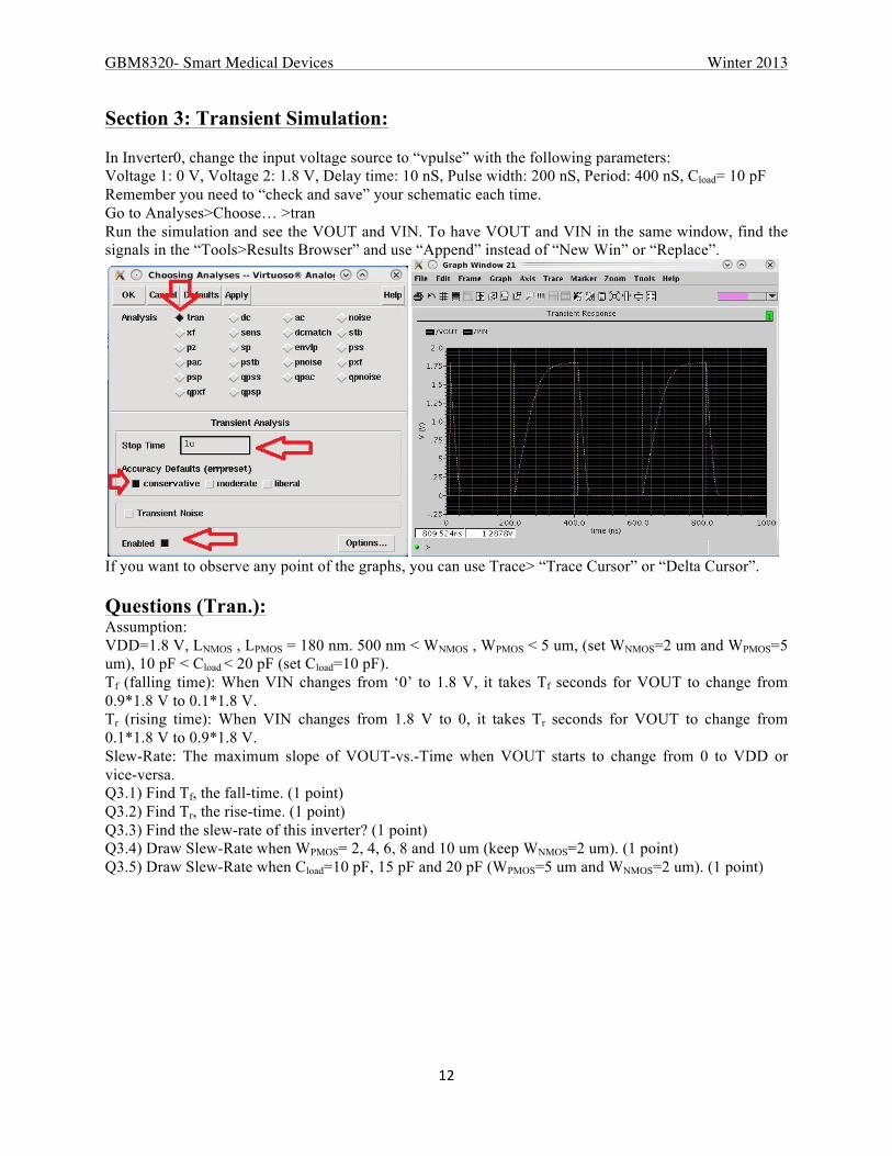
Section 3: Transient Simulation: In Inverter0, change the input voltage source to “vpulse” with the following parameters: Voltage 1: 0 V, Voltage 2: 1.8 V, Delay time: 10 nS, Pulse width: 200 nS, Period: 400 nS, Cload= 10 pF Remember you need to “check and save” your schematic each time. Go to Analyses>Choose… >tran Run the simulation and see the VOUT and VIN. To have VOUT and VIN in the same window, find the signals in the “Tools>Results Browser” and use “Append” instead of “New Win” or “Replace”.
If you want to observe any point of the graphs, you can use Trace> “Trace Cursor” or “Delta Cursor”. Questions (Tran.): Assumption: VDD=1.8 V, LNMOS , LPMOS = 180 nm. 500 nm < WNMOS , WPMOS < 5 um, (set WNMOS=2 um and WPMOS=5 um), 10 pF < Cload < 20 pF (set Cload=10 pF). Tf (falling time): When VIN changes from ‘0’ to 1.8 V, it takes Tf seconds for VOUT to change from 0.9*1.8 V to 0.1*1.8 V. Tr (rising time): When VIN changes from 1.8 V to 0, it takes Tr seconds for VOUT to change from 0.1*1.8 V to 0.9*1.8 V. Slew-Rate: The maximum slope of VOUT-vs.-Time when VOUT starts to change from 0 to VDD or vice-versa. Q3.1) Find Tf, the fall-time. (1 point) Q3.2) Find Tr, the rise-time. (1 point) Q3.3) Find the slew-rate of this inverter? (1 point) Q3.4) Draw Slew-Rate when WPMOS= 2, 4, 6, 8 and 10 um (keep WNMOS=2 um). (1 point) Q3.5) Draw Slew-Rate when Cload=10 pF, 15 pF and 20 pF (WPMOS=5 um and WNMOS=2 um). (1 point)

GBM8320- Smart Medical Devices Winter 2013
13
Section 4: AC Simulation: Change the input source to “vac” or “vsin”. AC magnitude: 1 V, DC voltage: 900 mV Go to Analyses>Choose…ac Sweep Variable: Frequency, Start: 1, Stop: 1 G, Sweep Type: Logarithmic, Point Per decade: 500 DC-Gain: Gain amplitude at very low frequency f-3dB: The frequency at which the Gain amplitude is 3 dB less than DC-Gain fT: The frequency at which the Gain amplitude becomes 1 (0 dB) Questions (AC): Q4.1) Find the DC-Gain? (1 point) Q4.2) Find f-3dB? (1 point) Q4.3) Draw DC-Gain and f-3dB when WPMOS = 3, 4, 5, 6, 7, 8 um (WNMOS=2 um, Cload=10 pF). (2 points) Q4.4) Draw DC-Gain and f-3dB when WNMOS = 1.6, 1.8, 2, 2.2, 2.4 um (WPMOS=6 um, Cload=10 pF). (2 points) Q4.5) Draw f-3dB when Cload = 10, 15, 20 pF (WPMOS=6 um, WNMOS=2 um). (1 point) Q4.6) How much is fT, the unity-gain frequency (WPMOS=6 um, WNMOS=2 um, Cload=10 pF)? (1 point)
GBM8320- Smart Medical Devices Winter 2013
14
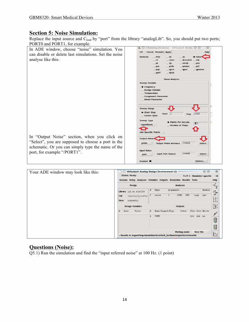
Section 5: Noise Simulation: Replace the input source and Cload by “port” from the library “analogLib”. So, you should put two ports; PORT0 and PORT1, for example. In ADE window, choose “noise” simulation. You can disable or delete last simulations. Set the noise analyse like this: In “Output Noise” section, when you click on “Select”, you are supposed to choose a port in the schematic. Or you can simply type the name of the port, for example “/PORT1”.
Your ADE window may look like this:
Questions (Noise): Q5.1) Run the simulation and find the “input referred noise” at 100 Hz. (1 point)
GBM8320- Smart Medical Devices Winter 2013
15
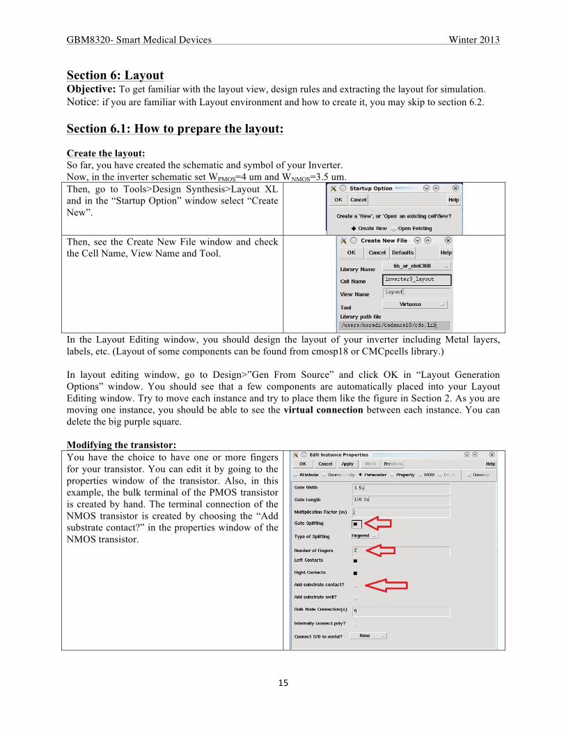
Section 6: Layout Objective: To get familiar with the layout view, design rules and extracting the layout for simulation. Notice: if you are familiar with Layout environment and how to create it, you may skip to section 6.2. Section 6.1: How to prepare the layout: Create the layout: So far, you have created the schematic and symbol of your Inverter. Now, in the inverter schematic set WPMOS=4 um and WNMOS=3.5 um. Then, go to Tools>Design Synthesis>Layout XL and in the “Startup Option” window select “Create New”.
Then, see the Create New File window and check the Cell Name, View Name and Tool.
In the Layout Editing window, you should design the layout of your inverter including Metal layers, labels, etc. (Layout of some components can be found from cmosp18 or CMCpcells library.) In layout editing window, go to Design>”Gen From Source” and click OK in “Layout Generation Options” window. You should see that a few components are automatically placed into your Layout Editing window. Try to move each instance and try to place them like the figure in Section 2. As you are moving one instance, you should be able to see the virtual connection between each instance. You can delete the big purple square. Modifying the transistor: You have the choice to have one or more fingers for your transistor. You can edit it by going to the properties window of the transistor. Also, in this example, the bulk terminal of the PMOS transistor is created by hand. The terminal connection of the NMOS transistor is created by choosing the “Add substrate contact?” in the properties window of the NMOS transistor.
GBM8320- Smart Medical Devices Winter 2013
16
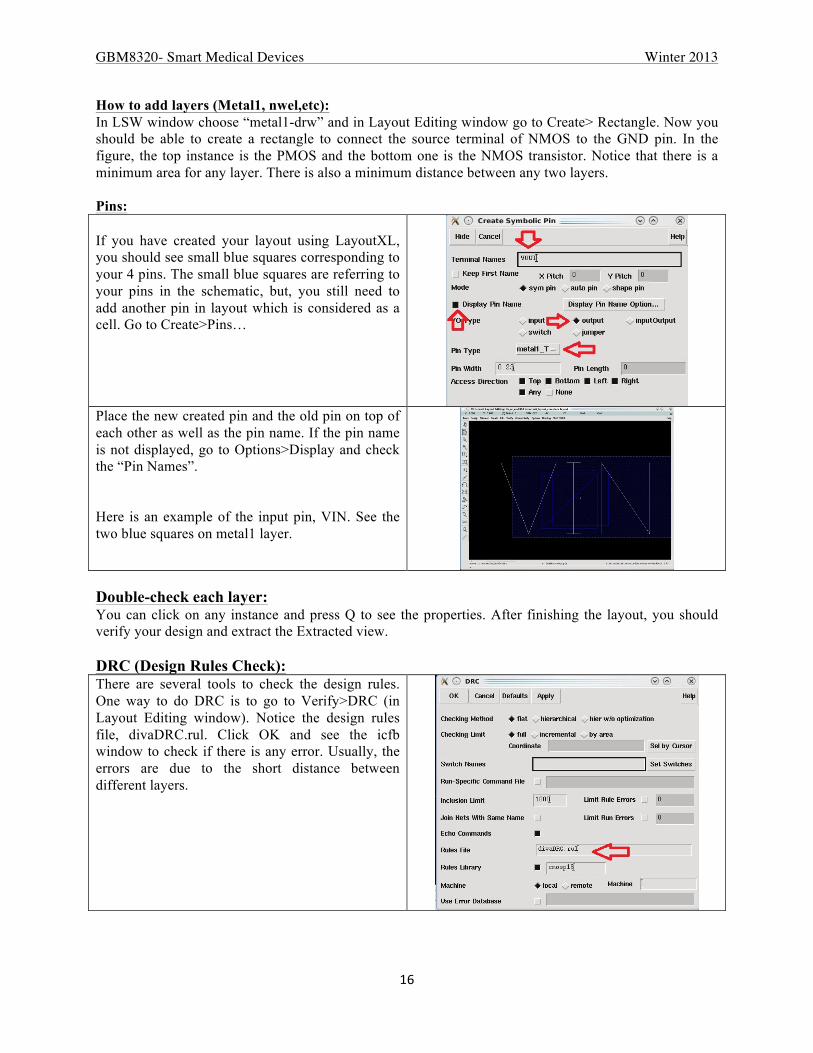
How to add layers (Metal1, nwel,etc): In LSW window choose “metal1-drw” and in Layout Editing window go to Create> Rectangle. Now you should be able to create a rectangle to connect the source terminal of NMOS to the GND pin. In the figure, the top instance is the PMOS and the bottom one is the NMOS transistor. Notice that there is a minimum area for any layer. There is also a minimum distance between any two layers. Pins: If you have created your layout using LayoutXL, you should see small blue squares corresponding to your 4 pins. The small blue squares are referring to your pins in the schematic, but, you still need to add another pin in layout which is considered as a cell. Go to Create>Pins…
Place the new created pin and the old pin on top of each other as well as the pin name. If the pin name is not displayed, go to Options>Display and check the “Pin Names”. Here is an example of the input pin, VIN. See the two blue squares on metal1 layer.
Double-check each layer: You can click on any instance and press Q to see the properties. After finishing the layout, you should verify your design and extract the Extracted view. DRC (Design Rules Check): There are several tools to check the design rules. One way to do DRC is to go to Verify>DRC (in Layout Editing window). Notice the design rules file, divaDRC.rul. Click OK and see the icfb window to check if there is any error. Usually, the errors are due to the short distance between different layers.
GBM8320- Smart Medical Devices Winter 2013
17
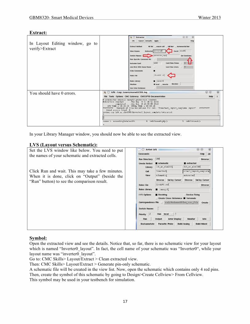
Extract: In Layout Editing window, go to verify>Extract
You should have 0 errors.
In your Library Manager window, you should now be able to see the extracted view. LVS (Layout versus Schematic): Set the LVS window like below. You need to put the names of your schematic and extracted cells. Click Run and wait. This may take a few minutes. When it is done, click on “Output” (beside the “Run” button) to see the comparison result.
Symbol: Open the extracted view and see the details. Notice that, so far, there is no schematic view for your layout which is named “Inverter0_layout”. In fact, the cell name of your schematic was “Inverter0“, while your layout name was “inverter0_layout”. Go to: CMC Skills> Layout/Extract > Clean extracted view. Then: CMC Skills> Layout/Extract > Generate pin-only schematic. A schematic file will be created in the view list. Now, open the schematic which contains only 4 red pins. Then, create the symbol of this schematic by going to Design>Create Cellview> From Cellview. This symbol may be used in your testbench for simulation.
GBM8320- Smart Medical Devices Winter 2013
18
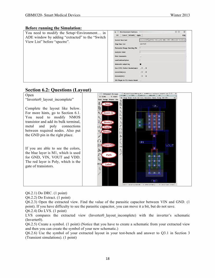
Before running the Simulation: You need to modify the Setup>Environment… in ADE window by adding “extracted” to the “Switch View List” before “spectre”.
Section 6.2: Questions (Layout) Open “Inverter0_layout_incomplete” Complete the layout like below. For more hints, go to Section 6.1. You need to modify NMOS transistor and add its bulk terminal, metal and poly connections between required nodes. Also put the GND pin in the right place. If you are able to see the colors, the blue layer is M1, which is used for GND, VIN, VOUT and VDD. The red layer is Poly, which is the gate of transistors.
Q6.2.1) Do DRC. (1 point) Q6.2.2) Do Extract. (1 point) Q6.2.3) Open the extracted view. Find the value of the parasitic capacitor between VIN and GND. (1 point). If you have difficulty to see the parasitic capacitor, you can move it a bit, but do not save. Q6.2.4) Do LVS. (1 point) LVS compares the extracted view (Inverter0_layout_incomplete) with the inverter’s schematic (Inverter0). Q6.2.5) Create a symbol. (1 point) (Notice that you have to create a schematic from your extracted view and then you can create the symbol of your new schematic.) Q6.2.6) Use the symbol of your extracted layout in your test-bench and answer to Q3.1 in Section 3 (Transient simulations). (1 point)