Embed Size (px)
Citation preview
EECS 141: Spring 2006 Bill Hung and Dennis Wang
University of California, Berkeley 1 © 2006
Cadence Layout for SRAM Phase I Bill Hung, Dennis Wang
Table of Contents
Cadence Layout for SRAM Phase I .................................................................................... 1
Opening a New Layout and New Library ................................................................... 2
SRAM Cell Transistors Layout....................................................................................... 5
Drawing NMOS .......................................................................................................... 5
Exploring Cadence Transistor Sizes ........................................................................... 7
NMOS ..................................................................................................................... 7
PMOS...................................................................................................................... 9
Testing NMOS and PMOS Extraction ...................................................................... 11
NMOS ................................................................................................................... 11
PMOS.................................................................................................................... 12
Half SRAM Cell Transistors Layout......................................................................... 13
Wiring within the SRAM Cell with Contacts ............................................................... 17
Contacts................................................................................................................. 18
Wiring word line ....................................................................................................... 19
Wiring BLBL−
, , QQ,−
and Vdd................................................................................... 20
Instantiate N-tap ........................................................................................................ 21
Minimizing Wires ..................................................................................................... 21
Connecting the Grounds............................................................................................ 22
Connecting the VDD................................................................................................. 24
Final Layout .................................................................................................................. 25
Testing with Repetitive Pattern ................................................................................. 26
APPENDIX ....................................................................................................................... 27
Cadence Shortcut Keys ................................................................................................. 27
Failure Notes, mistakes that I learned from trial and error ........................................... 27
HSPICE Minimum NMOS Extracted Netlist ............................................................... 28
HSPICE Minimum PMOS Extracted Netlist ................................................................ 29
HSPICE Q-bar between M1 NMOS drain and M2 PMOS drain.................................. 30
HSPICE Wiring BLBL−
, , QQ,−
and Vdd........................................................................ 31
HSPICE After Ground Metal 2 Rail ............................................................................. 32
HSPICE After Ground Metal 3 Connection.................................................................. 33
Final HSPICE SRAM Cell Extracted ........................................................................... 34
List of Tables Table 1 PMOS Dimensions in Library NCSU_TechLib_tsmc03d Layout......................... 5
Table 2 Minimum PMOS and NMOS Sizes from Library NCSU_TechLib_tsmc03d ...... 5
Table 3 Actual NMOS Size for Phrase I ............................................................................. 7
Table 4 Actual PMOS Size for Phrase I.............................................................................. 9
Table 5 Cadence Shortcut Keys ........................................................................................ 27
EECS 141: Spring 2006 Bill Hung and Dennis Wang
University of California, Berkeley 2 © 2006
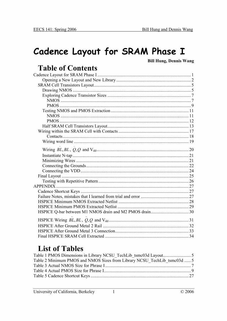
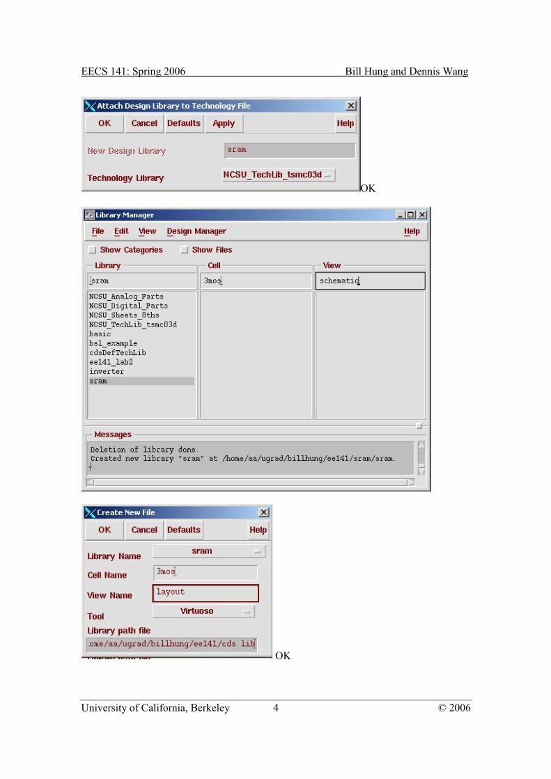
Opening a New Layout and New Library
File->New->Library
Put “sram” in Library field in Library Manager and press Enter.
EECS 141: Spring 2006 Bill Hung and Dennis Wang
University of California, Berkeley 3 © 2006
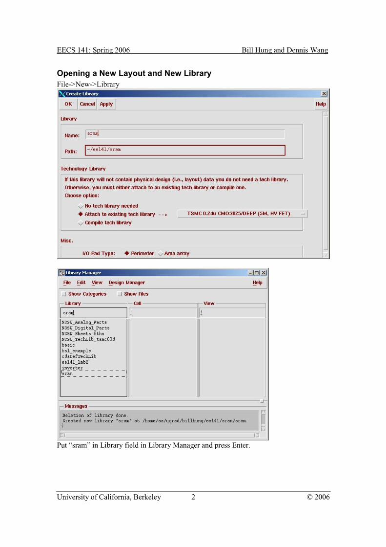
Make the folder and proceed.
OK
EECS 141: Spring 2006 Bill Hung and Dennis Wang
University of California, Berkeley 4 © 2006
OK
OK
EECS 141: Spring 2006 Bill Hung and Dennis Wang
University of California, Berkeley 5 © 2006
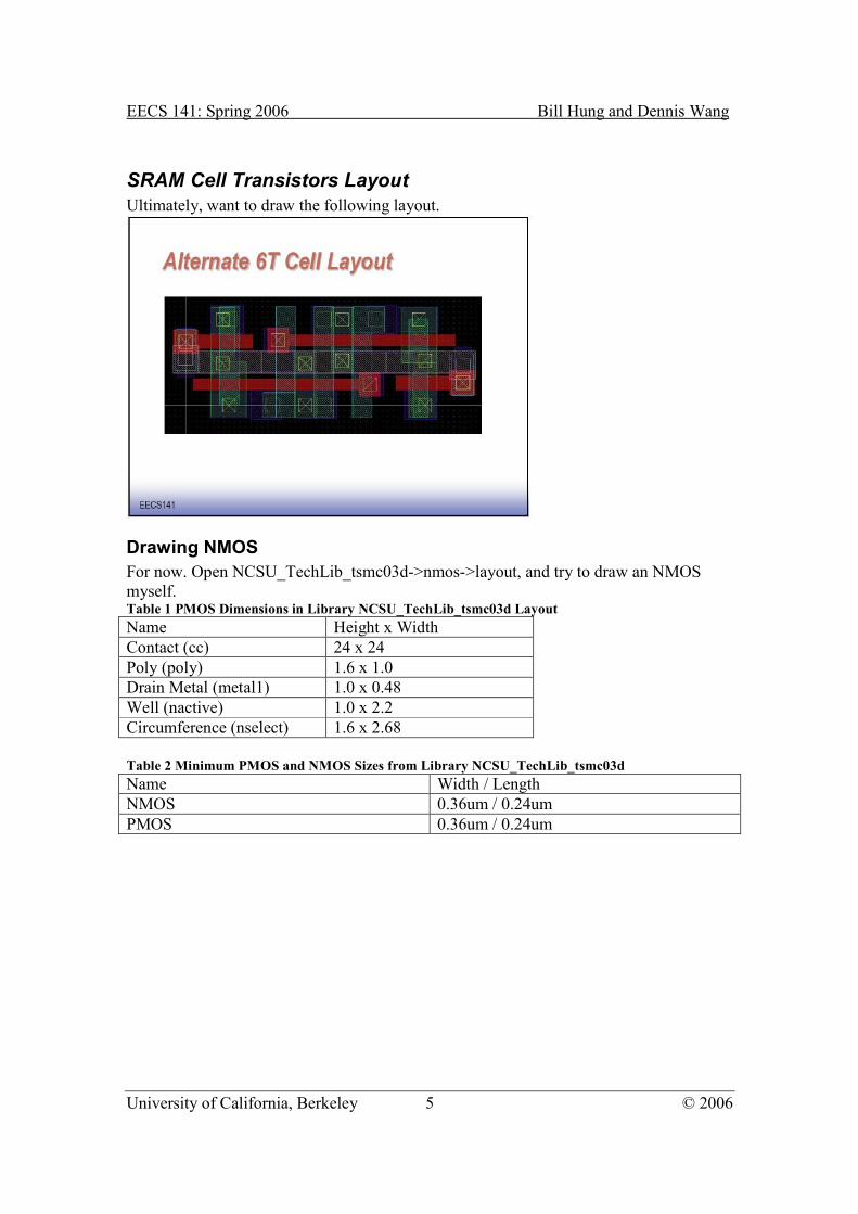
SRAM Cell Transistors Layout
Ultimately, want to draw the following layout.
Drawing NMOS
For now. Open NCSU_TechLib_tsmc03d->nmos->layout, and try to draw an NMOS
myself. Table 1 PMOS Dimensions in Library NCSU_TechLib_tsmc03d Layout
Name Height x Width
Contact (cc) 24 x 24
Poly (poly) 1.6 x 1.0
Drain Metal (metal1) 1.0 x 0.48
Well (nactive) 1.0 x 2.2
Circumference (nselect) 1.6 x 2.68
Table 2 Minimum PMOS and NMOS Sizes from Library NCSU_TechLib_tsmc03d
Name Width / Length
NMOS 0.36um / 0.24um
PMOS 0.36um / 0.24um
EECS 141: Spring 2006 Bill Hung and Dennis Wang
University of California, Berkeley 6 © 2006
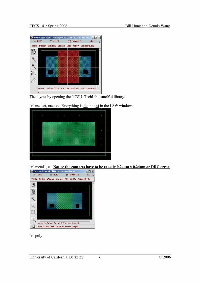
The layout by opening the NCSU_TechLib_tsmc03d library.
“r” nselect, nactive. Everything is dg, not nt in the LSW window.
“r” metal1, cc. Notice the contacts have to be exactly 0.24um x 0.24um or DRC error.
“r” poly
EECS 141: Spring 2006 Bill Hung and Dennis Wang
University of California, Berkeley 7 © 2006
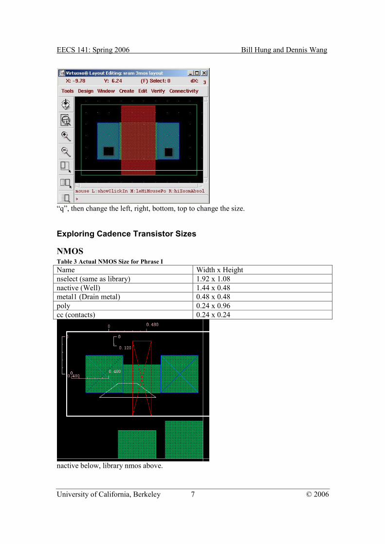
“q”, then change the left, right, bottom, top to change the size.
Exploring Cadence Transistor Sizes
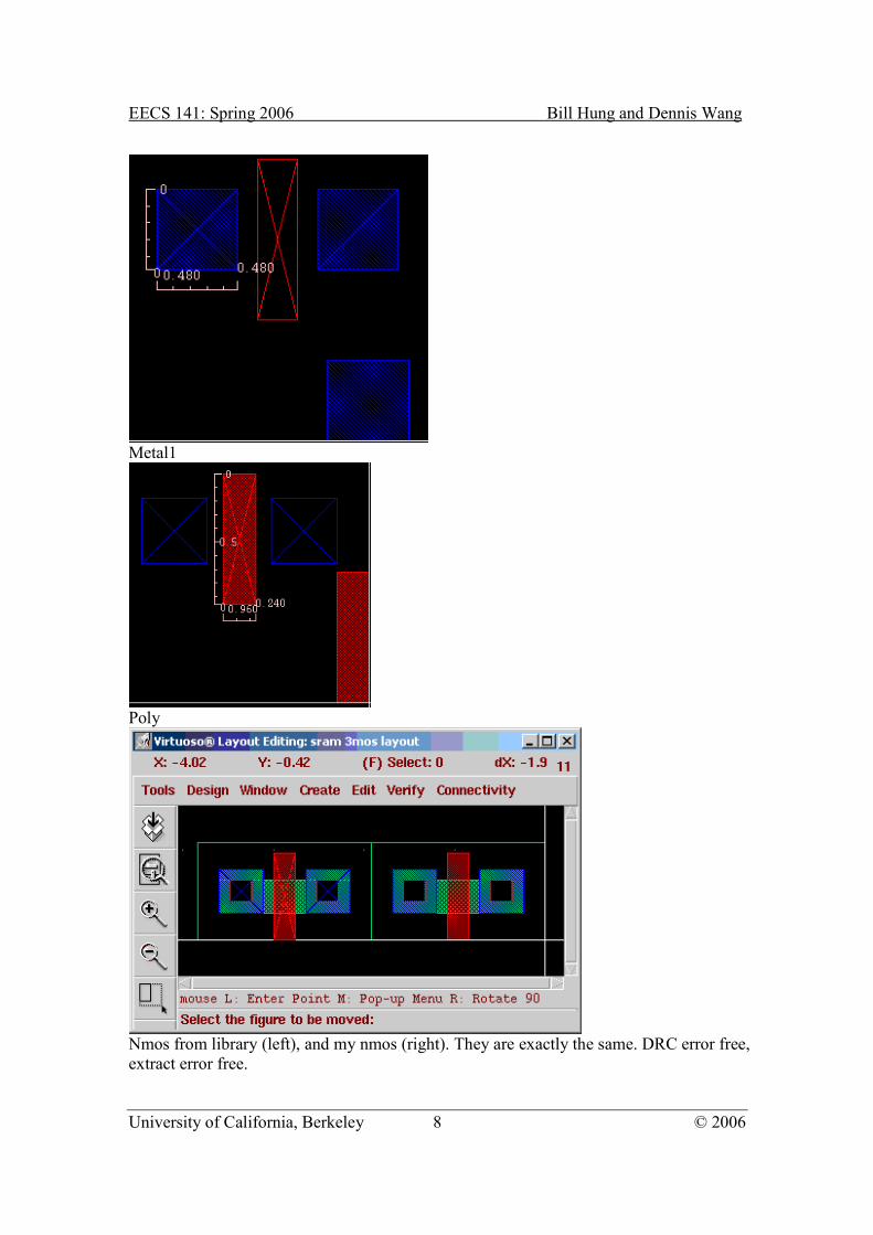
NMOS Table 3 Actual NMOS Size for Phrase I
Name Width x Height
nselect (same as library) 1.92 x 1.08
nactive (Well) 1.44 x 0.48
metal1 (Drain metal) 0.48 x 0.48
poly 0.24 x 0.96
cc (contacts) 0.24 x 0.24
nactive below, library nmos above.
EECS 141: Spring 2006 Bill Hung and Dennis Wang
University of California, Berkeley 8 © 2006
Metal1
Poly
Nmos from library (left), and my nmos (right). They are exactly the same. DRC error free,
extract error free.
EECS 141: Spring 2006 Bill Hung and Dennis Wang
University of California, Berkeley 9 © 2006
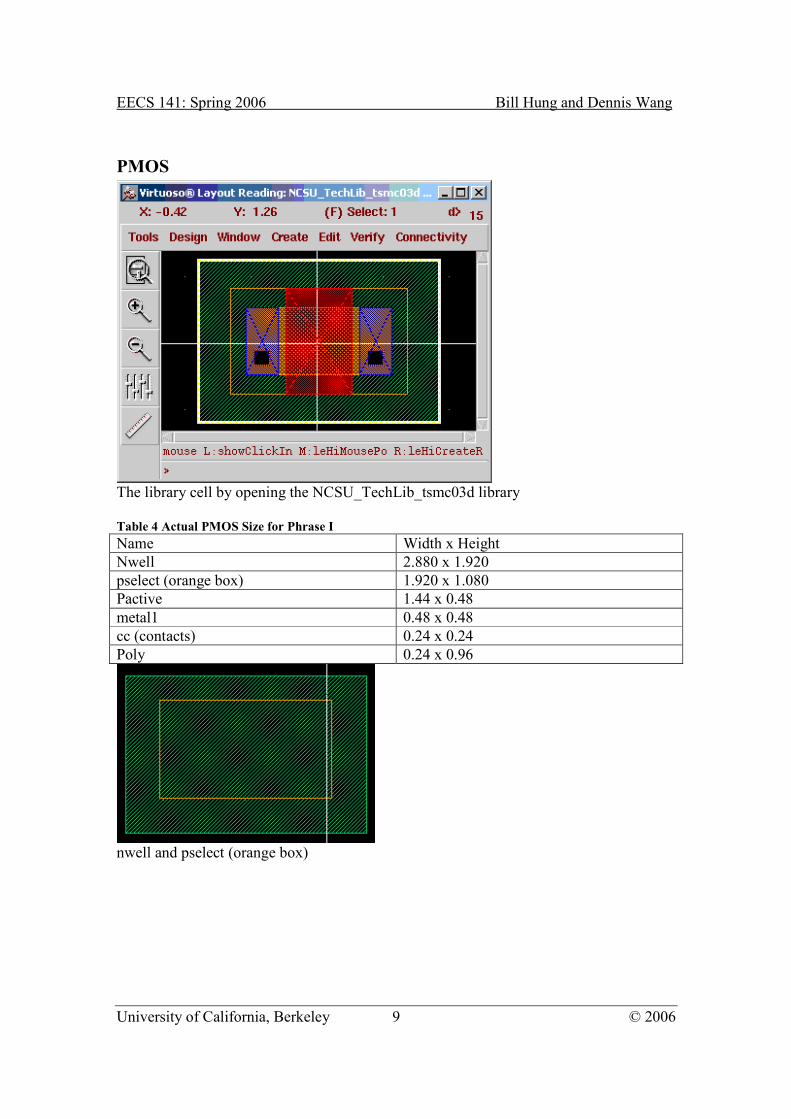
PMOS
The library cell by opening the NCSU_TechLib_tsmc03d library
Table 4 Actual PMOS Size for Phrase I
Name Width x Height
Nwell 2.880 x 1.920
pselect (orange box) 1.920 x 1.080
Pactive 1.44 x 0.48
metal1 0.48 x 0.48
cc (contacts) 0.24 x 0.24
Poly 0.24 x 0.96
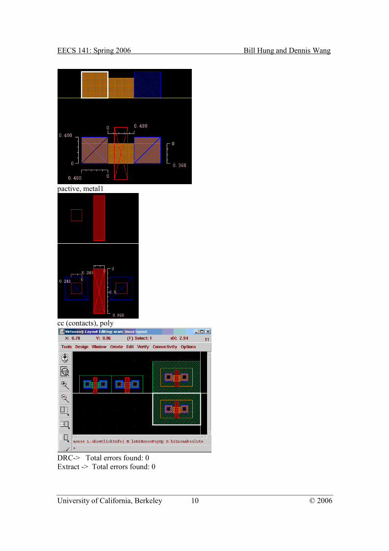
nwell and pselect (orange box)
EECS 141: Spring 2006 Bill Hung and Dennis Wang
University of California, Berkeley 10 © 2006
pactive, metal1
cc (contacts), poly
DRC-> Total errors found: 0
Extract -> Total errors found: 0
EECS 141: Spring 2006 Bill Hung and Dennis Wang
University of California, Berkeley 11 © 2006
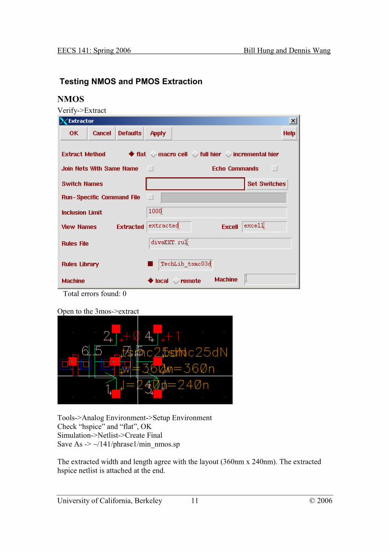
Testing NMOS and PMOS Extraction
NMOS
Verify->Extract
Total errors found: 0
Open to the 3mos->extract
Tools->Analog Environment->Setup Environment
Check “hspice” and “flat”, OK
Simulation->Netlist->Create Final
Save As -> ~/141/phrase1/min_nmos.sp
The extracted width and length agree with the layout (360nm x 240nm). The extracted
hspice netlist is attached at the end.
EECS 141: Spring 2006 Bill Hung and Dennis Wang
University of California, Berkeley 12 © 2006
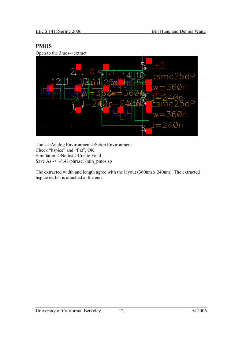
PMOS
Open to the 3mos->extract
Tools->Analog Environment->Setup Environment
Check “hspice” and “flat”, OK
Simulation->Netlist->Create Final
Save As -> ~/141/phrase1/min_pmos.sp
The extracted width and length agree with the layout (360nm x 240nm). The extracted
hspice netlist is attached at the end.
EECS 141: Spring 2006 Bill Hung and Dennis Wang
University of California, Berkeley 13 © 2006
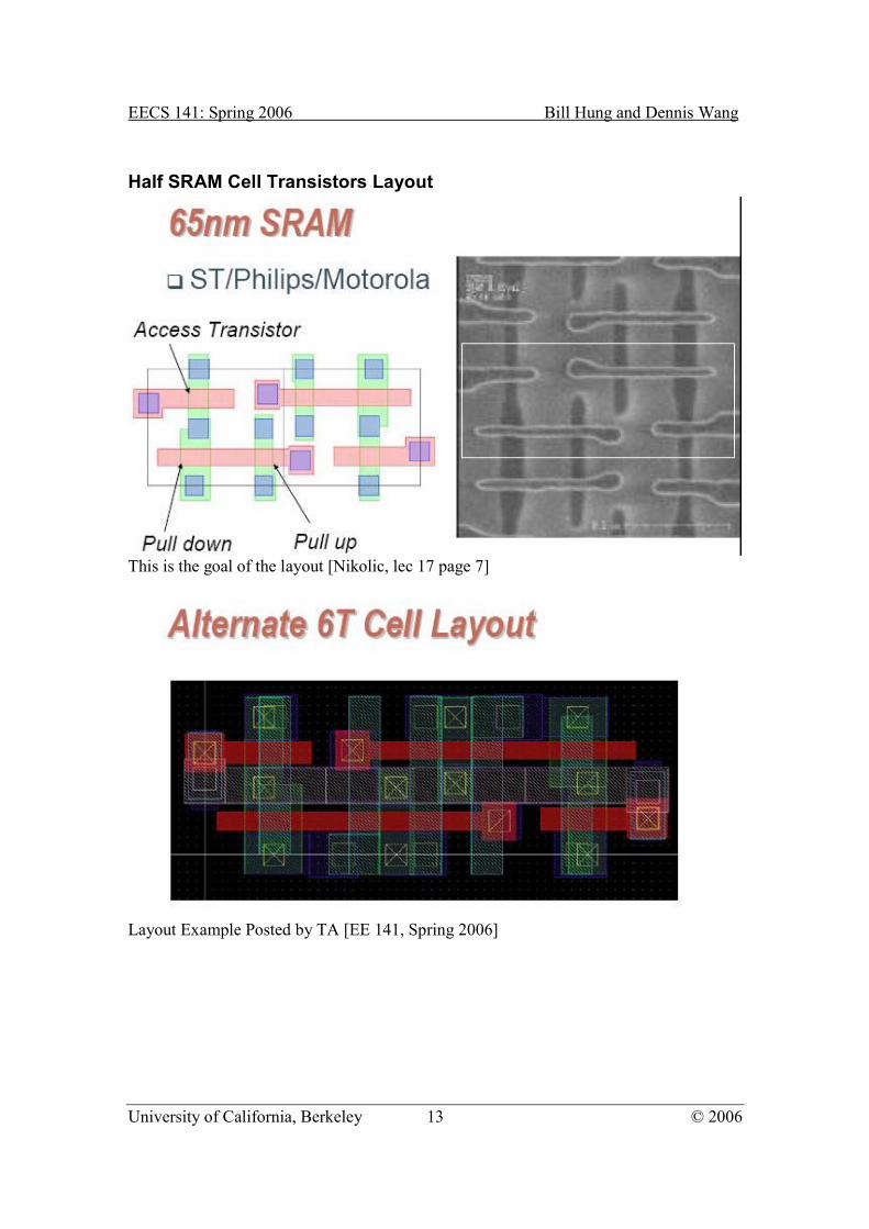
Half SRAM Cell Transistors Layout
This is the goal of the layout [Nikolic, lec 17 page 7]
Layout Example Posted by TA [EE 141, Spring 2006]
EECS 141: Spring 2006 Bill Hung and Dennis Wang
University of California, Berkeley 14 © 2006
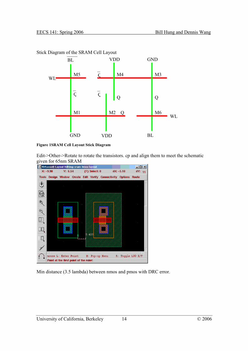
Stick Diagram of the SRAM Cell Layout
Figure 1SRAM Cell Layout Stick Diagram
Edit->Other->Rotate to rotate the transistors. cp and align them to meet the schematic
given for 65nm SRAM
Min distance (3.5 lambda) between nmos and pmos with DRC error.
BL
WL M5
Q
M1
GND VDD
Q
M2 Q
M4 M3
M6
Q
VDD
Q Q
GND
WL
BL
EECS 141: Spring 2006 Bill Hung and Dennis Wang
University of California, Berkeley 15 © 2006
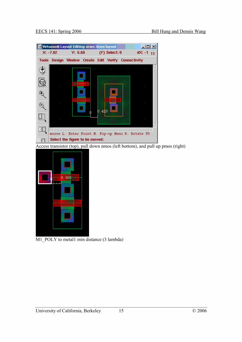
Access transistor (top), pull down nmos (left bottom), and pull up pmos (right)
M1_POLY to metal1 min distance (3 lambda)
EECS 141: Spring 2006 Bill Hung and Dennis Wang
University of California, Berkeley 16 © 2006
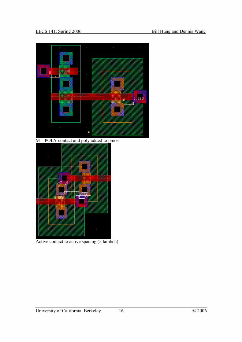
M1_POLY contact and poly added to pmos
Active contact to active spacing (5 lambda)
EECS 141: Spring 2006 Bill Hung and Dennis Wang
University of California, Berkeley 17 © 2006
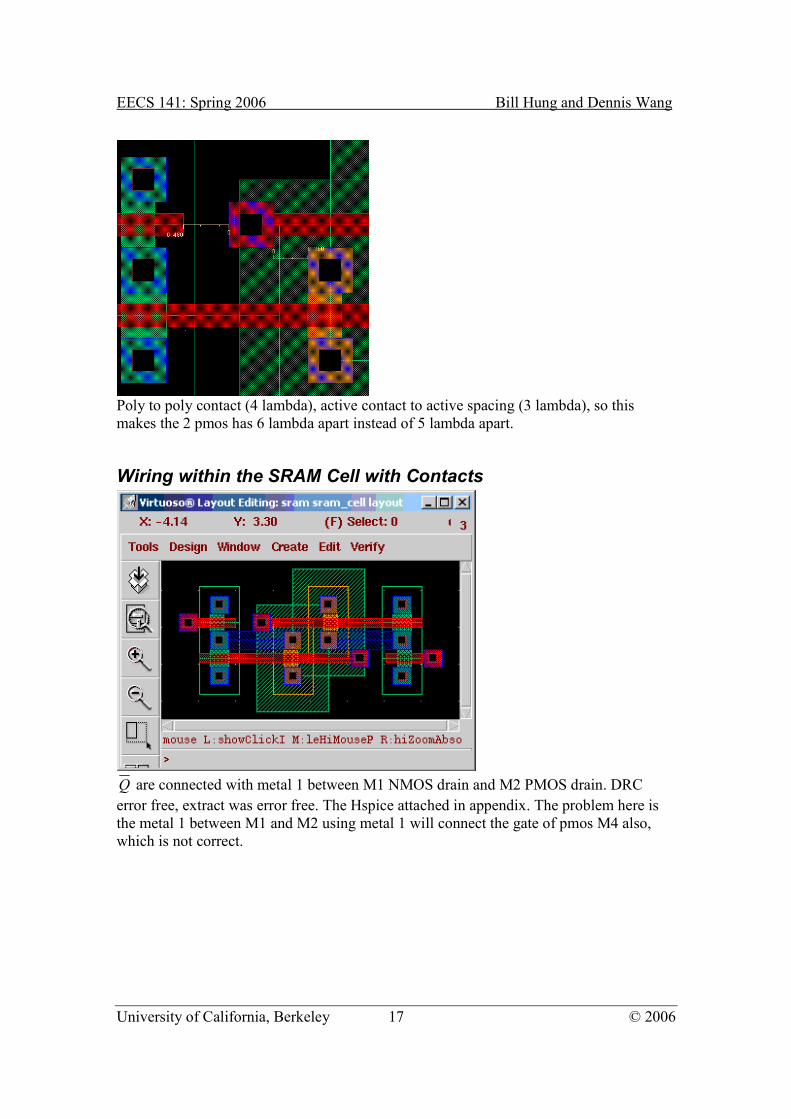
Poly to poly contact (4 lambda), active contact to active spacing (3 lambda), so this
makes the 2 pmos has 6 lambda apart instead of 5 lambda apart.
Wiring within the SRAM Cell with Contacts
Q are connected with metal 1 between M1 NMOS drain and M2 PMOS drain. DRC
error free, extract was error free. The Hspice attached in appendix. The problem here is
the metal 1 between M1 and M2 using metal 1 will connect the gate of pmos M4 also,
which is not correct.
EECS 141: Spring 2006 Bill Hung and Dennis Wang
University of California, Berkeley 18 © 2006
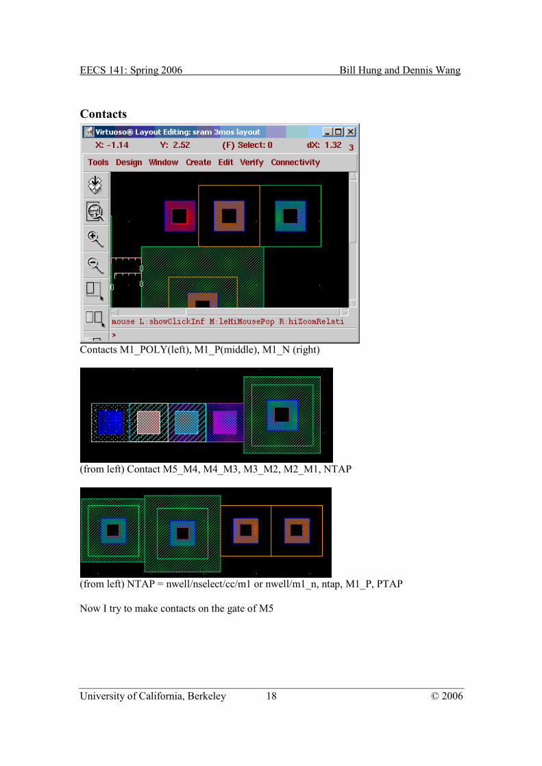
Contacts
Contacts M1_POLY(left), M1_P(middle), M1_N (right)
(from left) Contact M5_M4, M4_M3, M3_M2, M2_M1, NTAP
(from left) NTAP = nwell/nselect/cc/m1 or nwell/m1_n, ntap, M1_P, PTAP
Now I try to make contacts on the gate of M5
EECS 141: Spring 2006 Bill Hung and Dennis Wang
University of California, Berkeley 19 © 2006
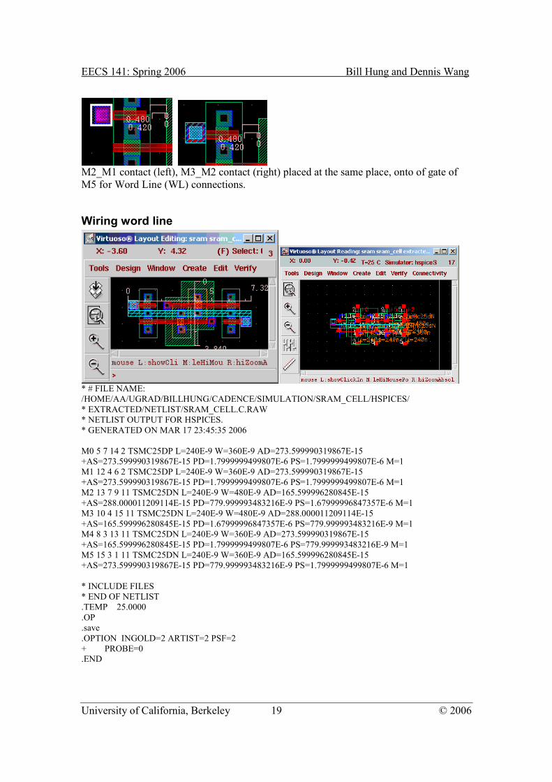
M2_M1 contact (left), M3_M2 contact (right) placed at the same place, onto of gate of
M5 for Word Line (WL) connections.
Wiring word line
* # FILE NAME:
/HOME/AA/UGRAD/BILLHUNG/CADENCE/SIMULATION/SRAM_CELL/HSPICES/
* EXTRACTED/NETLIST/SRAM_CELL.C.RAW
* NETLIST OUTPUT FOR HSPICES.
* GENERATED ON MAR 17 23:45:35 2006
M0 5 7 14 2 TSMC25DP L=240E-9 W=360E-9 AD=273.599990319867E-15
+AS=273.599990319867E-15 PD=1.7999999499807E-6 PS=1.7999999499807E-6 M=1
M1 12 4 6 2 TSMC25DP L=240E-9 W=360E-9 AD=273.599990319867E-15
+AS=273.599990319867E-15 PD=1.7999999499807E-6 PS=1.7999999499807E-6 M=1
M2 13 7 9 11 TSMC25DN L=240E-9 W=480E-9 AD=165.599996280845E-15
+AS=288.000011209114E-15 PD=779.999993483216E-9 PS=1.67999996847357E-6 M=1
M3 10 4 15 11 TSMC25DN L=240E-9 W=480E-9 AD=288.000011209114E-15
+AS=165.599996280845E-15 PD=1.67999996847357E-6 PS=779.999993483216E-9 M=1
M4 8 3 13 11 TSMC25DN L=240E-9 W=360E-9 AD=273.599990319867E-15
+AS=165.599996280845E-15 PD=1.7999999499807E-6 PS=779.999993483216E-9 M=1
M5 15 3 1 11 TSMC25DN L=240E-9 W=360E-9 AD=165.599996280845E-15
+AS=273.599990319867E-15 PD=779.999993483216E-9 PS=1.7999999499807E-6 M=1
* INCLUDE FILES
* END OF NETLIST
.TEMP 25.0000
.OP
.save
.OPTION INGOLD=2 ARTIST=2 PSF=2
+ PROBE=0
.END
EECS 141: Spring 2006 Bill Hung and Dennis Wang
University of California, Berkeley 20 © 2006
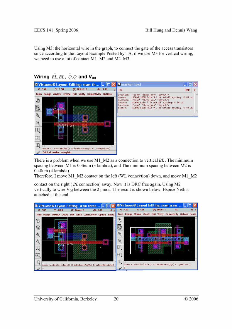
Using M3, the horizontal wire in the graph, to connect the gate of the access transistors
since according to the Layout Example Posted by TA, if we use M3 for vertical wiring,
we need to use a lot of contact M1_M2 and M2_M3.
Wiring BLBL−
, , QQ,−
and Vdd
There is a problem when we use M1_M2 as a connection to vertical−
BL . The minimum
spacing between M1 is 0.36um (3 lambda), and The minimum spacing between M2 is
0.48um (4 lambda).
Therefore, I move M1_M2 contact on the left (WL connection) down, and move M1_M2
contact on the right (−
BL connection) away. Now it is DRC free again. Using M2
vertically to wire Vdd between the 2 pmos. The result is shown below. Hspice Netlist
attached at the end.
EECS 141: Spring 2006 Bill Hung and Dennis Wang
University of California, Berkeley 21 © 2006
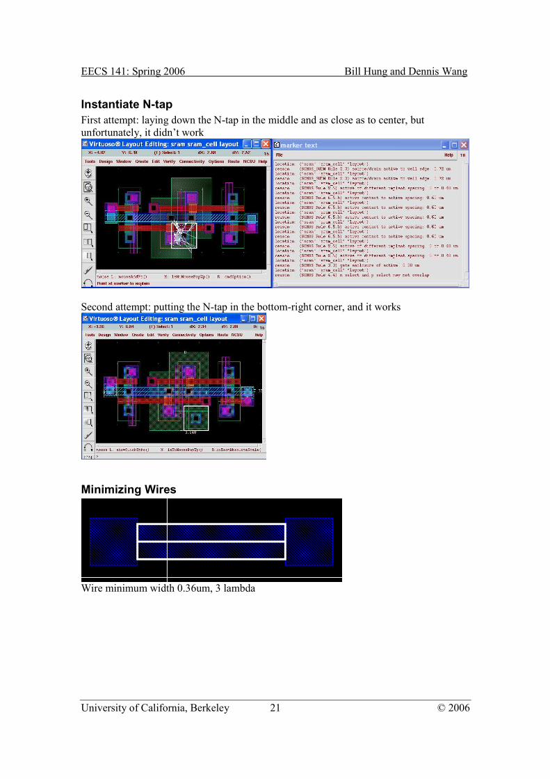
Instantiate N-tap
First attempt: laying down the N-tap in the middle and as close as to center, but
unfortunately, it didn’t work
Second attempt: putting the N-tap in the bottom-right corner, and it works
Minimizing Wires
Wire minimum width 0.36um, 3 lambda
EECS 141: Spring 2006 Bill Hung and Dennis Wang
University of California, Berkeley 22 © 2006
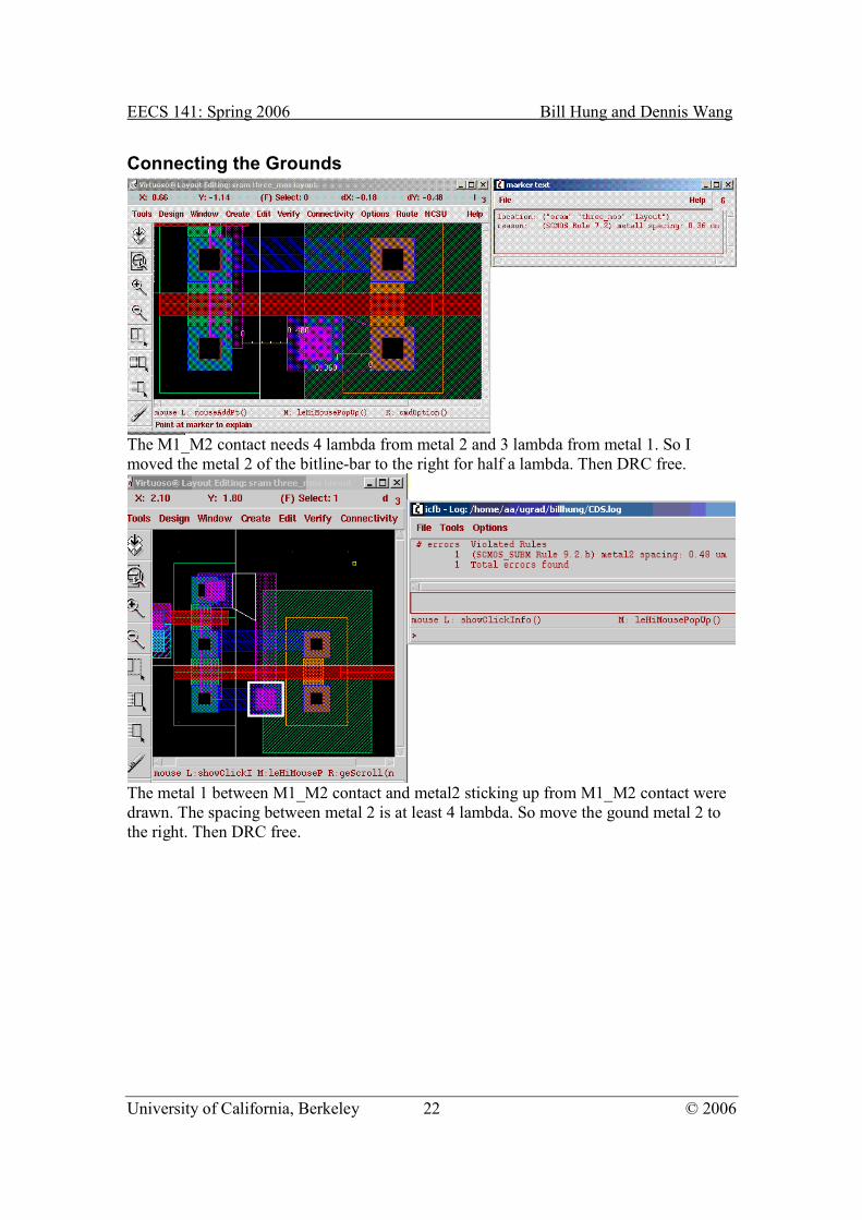
Connecting the Grounds
The M1_M2 contact needs 4 lambda from metal 2 and 3 lambda from metal 1. So I
moved the metal 2 of the bitline-bar to the right for half a lambda. Then DRC free.
The metal 1 between M1_M2 contact and metal2 sticking up from M1_M2 contact were
drawn. The spacing between metal 2 is at least 4 lambda. So move the gound metal 2 to
the right. Then DRC free.
EECS 141: Spring 2006 Bill Hung and Dennis Wang
University of California, Berkeley 23 © 2006
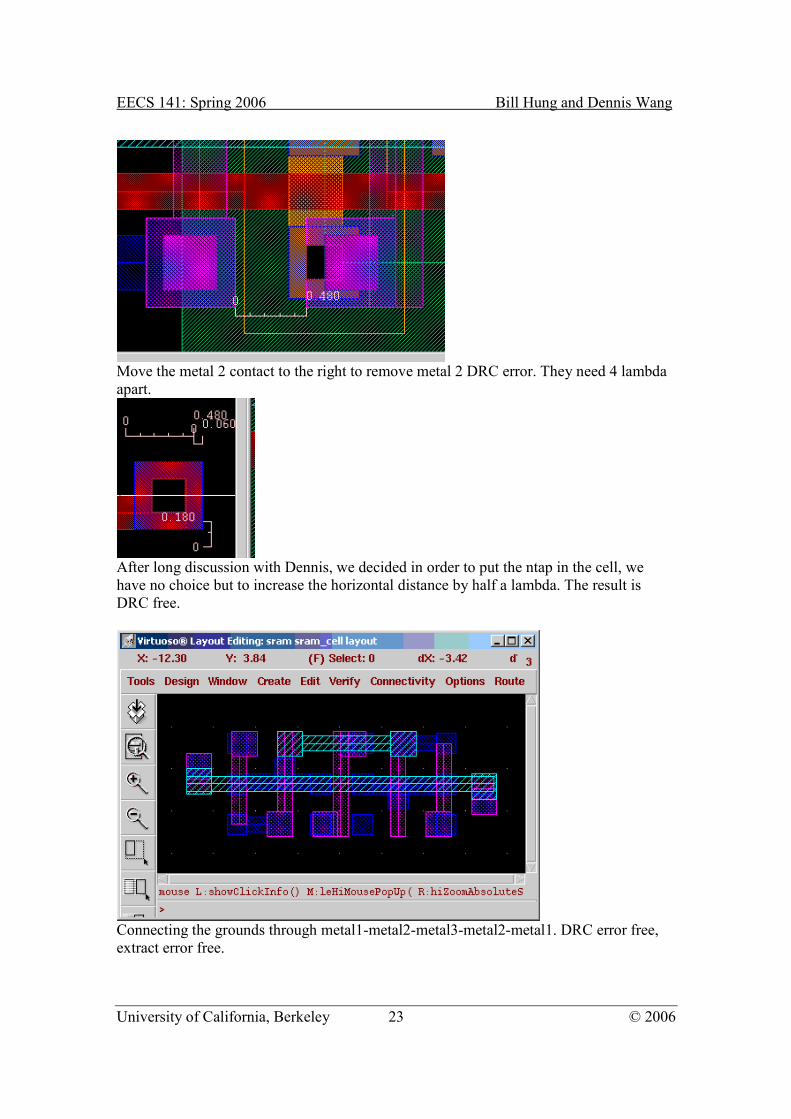
Move the metal 2 contact to the right to remove metal 2 DRC error. They need 4 lambda
apart.
After long discussion with Dennis, we decided in order to put the ntap in the cell, we
have no choice but to increase the horizontal distance by half a lambda. The result is
DRC free.
Connecting the grounds through metal1-metal2-metal3-metal2-metal1. DRC error free,
extract error free.
EECS 141: Spring 2006 Bill Hung and Dennis Wang
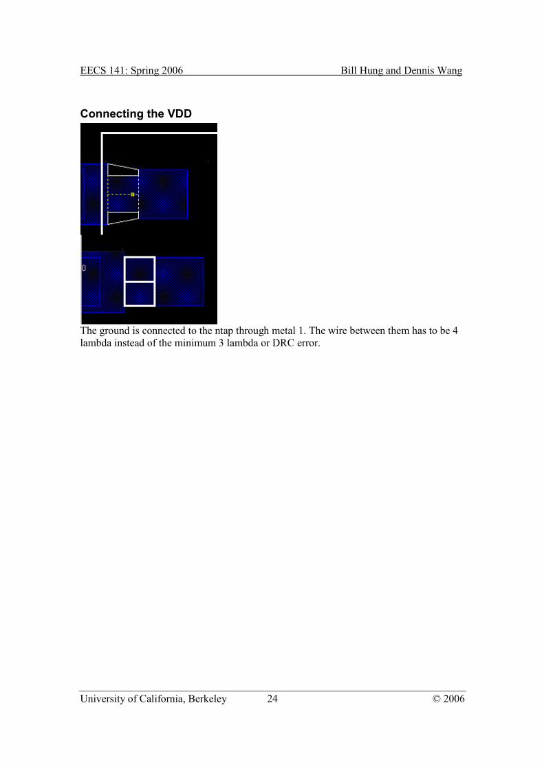
University of California, Berkeley 24 © 2006
Connecting the VDD
The ground is connected to the ntap through metal 1. The wire between them has to be 4
lambda instead of the minimum 3 lambda or DRC error.
EECS 141: Spring 2006 Bill Hung and Dennis Wang
University of California, Berkeley 25 © 2006
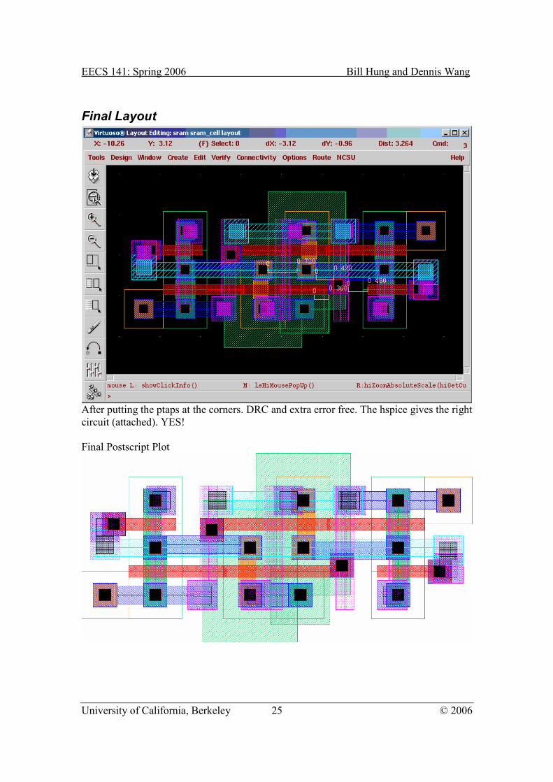
Final Layout
After putting the ptaps at the corners. DRC and extra error free. The hspice gives the right
circuit (attached). YES!
Final Postscript Plot
EECS 141: Spring 2006 Bill Hung and Dennis Wang
University of California, Berkeley 26 © 2006
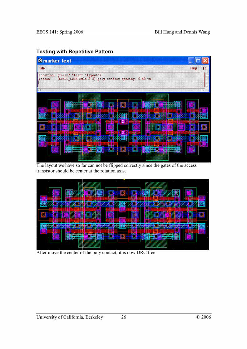
Testing with Repetitive Pattern
The layout we have so far can not be flipped correctly since the gates of the access
transistor should be center at the rotation axis.
After move the center of the poly contact, it is now DRC free
EECS 141: Spring 2006 Bill Hung and Dennis Wang
University of California, Berkeley 27 © 2006
APPENDIX
Cadence Shortcut Keys Table 5 Cadence Shortcut Keys
Shortcut Key Meaning
C Copy
M -> Flip Upside Down Flip
O Contact
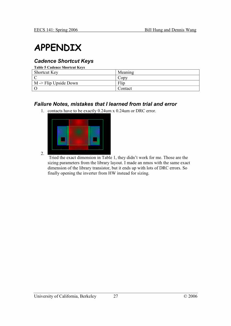
Failure Notes, mistakes that I learned from trial and error
1. contacts have to be exactly 0.24um x 0.24um or DRC error.
2. Tried the exact dimension in Table 1, they didn’t work for me. Those are the
sizing parameters from the library layout. I made an nmos with the same exact
dimension of the library transistor, but it ends up with lots of DRC errors. So
finally opening the inverter from HW instead for sizing.
EECS 141: Spring 2006 Bill Hung and Dennis Wang
University of California, Berkeley 28 © 2006
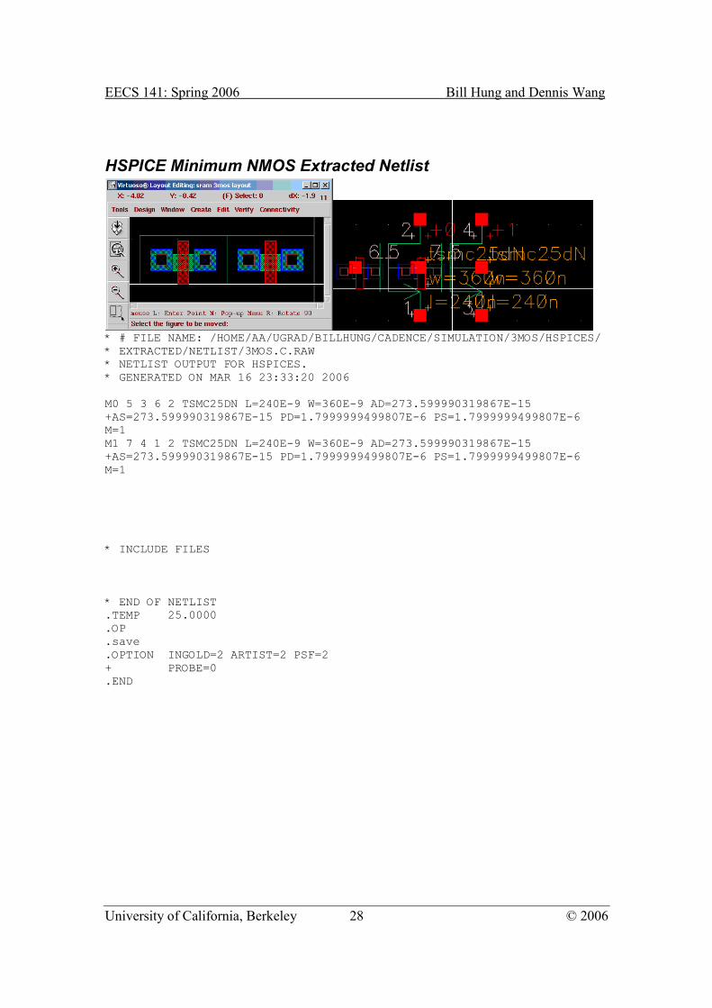
HSPICE Minimum NMOS Extracted Netlist
* # FILE NAME: /HOME/AA/UGRAD/BILLHUNG/CADENCE/SIMULATION/3MOS/HSPICES/ * EXTRACTED/NETLIST/3MOS.C.RAW * NETLIST OUTPUT FOR HSPICES. * GENERATED ON MAR 16 23:33:20 2006 M0 5 3 6 2 TSMC25DN L=240E-9 W=360E-9 AD=273.599990319867E-15 +AS=273.599990319867E-15 PD=1.7999999499807E-6 PS=1.7999999499807E-6 M=1 M1 7 4 1 2 TSMC25DN L=240E-9 W=360E-9 AD=273.599990319867E-15 +AS=273.599990319867E-15 PD=1.7999999499807E-6 PS=1.7999999499807E-6 M=1 * INCLUDE FILES * END OF NETLIST .TEMP 25.0000 .OP .save .OPTION INGOLD=2 ARTIST=2 PSF=2 + PROBE=0 .END
EECS 141: Spring 2006 Bill Hung and Dennis Wang
University of California, Berkeley 29 © 2006
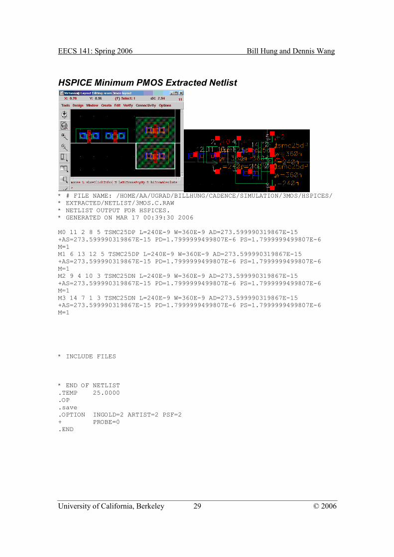
HSPICE Minimum PMOS Extracted Netlist
* # FILE NAME: /HOME/AA/UGRAD/BILLHUNG/CADENCE/SIMULATION/3MOS/HSPICES/ * EXTRACTED/NETLIST/3MOS.C.RAW * NETLIST OUTPUT FOR HSPICES. * GENERATED ON MAR 17 00:39:30 2006 M0 11 2 8 5 TSMC25DP L=240E-9 W=360E-9 AD=273.599990319867E-15 +AS=273.599990319867E-15 PD=1.7999999499807E-6 PS=1.7999999499807E-6 M=1 M1 6 13 12 5 TSMC25DP L=240E-9 W=360E-9 AD=273.599990319867E-15 +AS=273.599990319867E-15 PD=1.7999999499807E-6 PS=1.7999999499807E-6 M=1 M2 9 4 10 3 TSMC25DN L=240E-9 W=360E-9 AD=273.599990319867E-15 +AS=273.599990319867E-15 PD=1.7999999499807E-6 PS=1.7999999499807E-6 M=1 M3 14 7 1 3 TSMC25DN L=240E-9 W=360E-9 AD=273.599990319867E-15 +AS=273.599990319867E-15 PD=1.7999999499807E-6 PS=1.7999999499807E-6 M=1 * INCLUDE FILES * END OF NETLIST .TEMP 25.0000 .OP .save .OPTION INGOLD=2 ARTIST=2 PSF=2 + PROBE=0 .END
EECS 141: Spring 2006 Bill Hung and Dennis Wang
University of California, Berkeley 30 © 2006
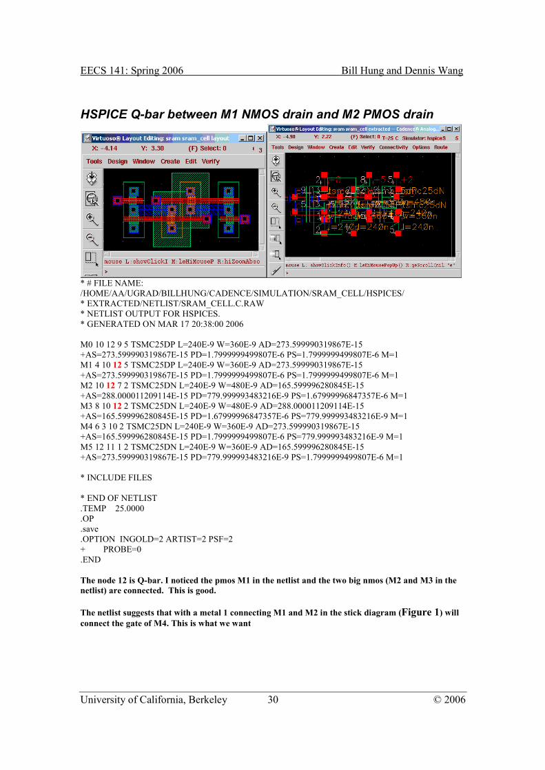
HSPICE Q-bar between M1 NMOS drain and M2 PMOS drain
* # FILE NAME:
/HOME/AA/UGRAD/BILLHUNG/CADENCE/SIMULATION/SRAM_CELL/HSPICES/
* EXTRACTED/NETLIST/SRAM_CELL.C.RAW
* NETLIST OUTPUT FOR HSPICES.
* GENERATED ON MAR 17 20:38:00 2006
M0 10 12 9 5 TSMC25DP L=240E-9 W=360E-9 AD=273.599990319867E-15
+AS=273.599990319867E-15 PD=1.7999999499807E-6 PS=1.7999999499807E-6 M=1
M1 4 10 12 5 TSMC25DP L=240E-9 W=360E-9 AD=273.599990319867E-15
+AS=273.599990319867E-15 PD=1.7999999499807E-6 PS=1.7999999499807E-6 M=1
M2 10 12 7 2 TSMC25DN L=240E-9 W=480E-9 AD=165.599996280845E-15
+AS=288.000011209114E-15 PD=779.999993483216E-9 PS=1.67999996847357E-6 M=1
M3 8 10 12 2 TSMC25DN L=240E-9 W=480E-9 AD=288.000011209114E-15
+AS=165.599996280845E-15 PD=1.67999996847357E-6 PS=779.999993483216E-9 M=1
M4 6 3 10 2 TSMC25DN L=240E-9 W=360E-9 AD=273.599990319867E-15
+AS=165.599996280845E-15 PD=1.7999999499807E-6 PS=779.999993483216E-9 M=1
M5 12 11 1 2 TSMC25DN L=240E-9 W=360E-9 AD=165.599996280845E-15
+AS=273.599990319867E-15 PD=779.999993483216E-9 PS=1.7999999499807E-6 M=1
* INCLUDE FILES
* END OF NETLIST
.TEMP 25.0000
.OP
.save
.OPTION INGOLD=2 ARTIST=2 PSF=2
+ PROBE=0
.END
The node 12 is Q-bar. I noticed the pmos M1 in the netlist and the two big nmos (M2 and M3 in the
netlist) are connected. This is good.
The netlist suggests that with a metal 1 connecting M1 and M2 in the stick diagram (Figure 1) will connect the gate of M4. This is what we want
EECS 141: Spring 2006 Bill Hung and Dennis Wang
University of California, Berkeley 31 © 2006
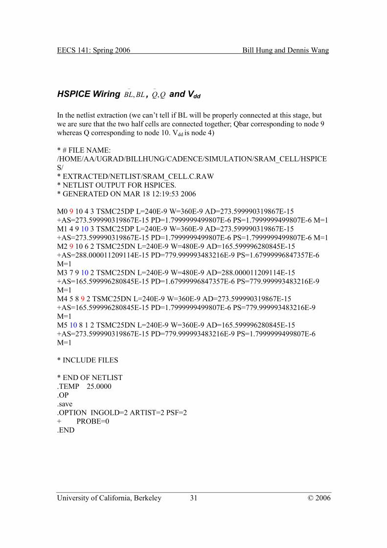
HSPICE Wiring BLBL−
, , QQ,−
and Vdd
In the netlist extraction (we can’t tell if BL will be properly connected at this stage, but
we are sure that the two half cells are connected together; Qbar corresponding to node 9
whereas Q corresponding to node 10. Vdd is node 4)
* # FILE NAME:
/HOME/AA/UGRAD/BILLHUNG/CADENCE/SIMULATION/SRAM_CELL/HSPICE
S/
* EXTRACTED/NETLIST/SRAM_CELL.C.RAW
* NETLIST OUTPUT FOR HSPICES.
* GENERATED ON MAR 18 12:19:53 2006
M0 9 10 4 3 TSMC25DP L=240E-9 W=360E-9 AD=273.599990319867E-15
+AS=273.599990319867E-15 PD=1.7999999499807E-6 PS=1.7999999499807E-6 M=1
M1 4 9 10 3 TSMC25DP L=240E-9 W=360E-9 AD=273.599990319867E-15
+AS=273.599990319867E-15 PD=1.7999999499807E-6 PS=1.7999999499807E-6 M=1
M2 9 10 6 2 TSMC25DN L=240E-9 W=480E-9 AD=165.599996280845E-15
+AS=288.000011209114E-15 PD=779.999993483216E-9 PS=1.67999996847357E-6
M=1
M3 7 9 10 2 TSMC25DN L=240E-9 W=480E-9 AD=288.000011209114E-15
+AS=165.599996280845E-15 PD=1.67999996847357E-6 PS=779.999993483216E-9
M=1
M4 5 8 9 2 TSMC25DN L=240E-9 W=360E-9 AD=273.599990319867E-15
+AS=165.599996280845E-15 PD=1.7999999499807E-6 PS=779.999993483216E-9
M=1
M5 10 8 1 2 TSMC25DN L=240E-9 W=360E-9 AD=165.599996280845E-15
+AS=273.599990319867E-15 PD=779.999993483216E-9 PS=1.7999999499807E-6
M=1
* INCLUDE FILES
* END OF NETLIST
.TEMP 25.0000
.OP
.save
.OPTION INGOLD=2 ARTIST=2 PSF=2
+ PROBE=0
.END
EECS 141: Spring 2006 Bill Hung and Dennis Wang
University of California, Berkeley 32 © 2006
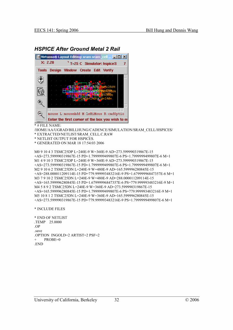
HSPICE After Ground Metal 2 Rail
* # FILE NAME:
/HOME/AA/UGRAD/BILLHUNG/CADENCE/SIMULATION/SRAM_CELL/HSPICES/
* EXTRACTED/NETLIST/SRAM_CELL.C.RAW
* NETLIST OUTPUT FOR HSPICES.
* GENERATED ON MAR 18 17:54:03 2006
M0 9 10 4 3 TSMC25DP L=240E-9 W=360E-9 AD=273.599990319867E-15
+AS=273.599990319867E-15 PD=1.7999999499807E-6 PS=1.7999999499807E-6 M=1
M1 4 9 10 3 TSMC25DP L=240E-9 W=360E-9 AD=273.599990319867E-15
+AS=273.599990319867E-15 PD=1.7999999499807E-6 PS=1.7999999499807E-6 M=1
M2 9 10 6 2 TSMC25DN L=240E-9 W=480E-9 AD=165.599996280845E-15
+AS=288.000011209114E-15 PD=779.999993483216E-9 PS=1.67999996847357E-6 M=1
M3 7 9 10 2 TSMC25DN L=240E-9 W=480E-9 AD=288.000011209114E-15
+AS=165.599996280845E-15 PD=1.67999996847357E-6 PS=779.999993483216E-9 M=1
M4 5 8 9 2 TSMC25DN L=240E-9 W=360E-9 AD=273.599990319867E-15
+AS=165.599996280845E-15 PD=1.7999999499807E-6 PS=779.999993483216E-9 M=1
M5 10 8 1 2 TSMC25DN L=240E-9 W=360E-9 AD=165.599996280845E-15
+AS=273.599990319867E-15 PD=779.999993483216E-9 PS=1.7999999499807E-6 M=1
* INCLUDE FILES
* END OF NETLIST
.TEMP 25.0000
.OP
.save
.OPTION INGOLD=2 ARTIST=2 PSF=2
+ PROBE=0
.END
EECS 141: Spring 2006 Bill Hung and Dennis Wang
University of California, Berkeley 33 © 2006
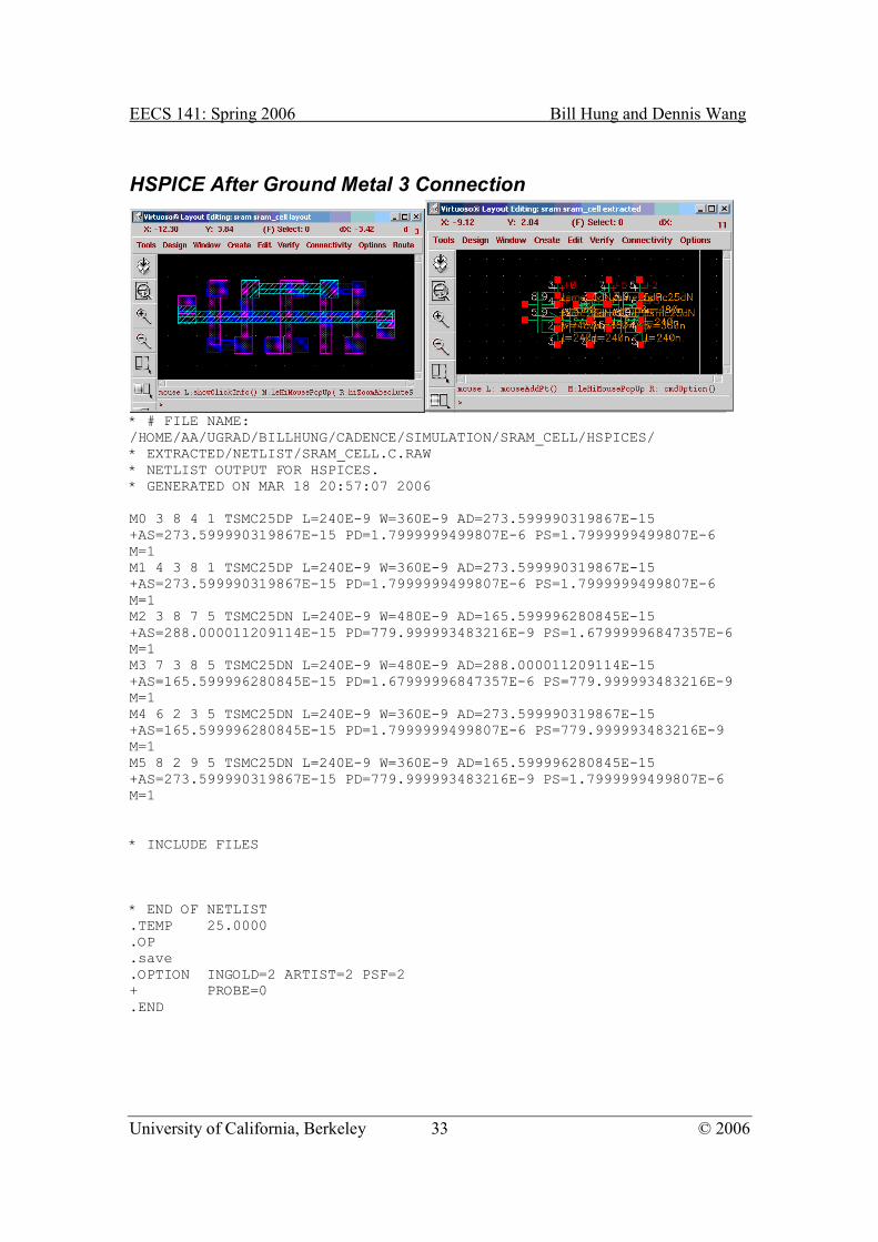
HSPICE After Ground Metal 3 Connection
* # FILE NAME: /HOME/AA/UGRAD/BILLHUNG/CADENCE/SIMULATION/SRAM_CELL/HSPICES/ * EXTRACTED/NETLIST/SRAM_CELL.C.RAW * NETLIST OUTPUT FOR HSPICES. * GENERATED ON MAR 18 20:57:07 2006 M0 3 8 4 1 TSMC25DP L=240E-9 W=360E-9 AD=273.599990319867E-15 +AS=273.599990319867E-15 PD=1.7999999499807E-6 PS=1.7999999499807E-6 M=1 M1 4 3 8 1 TSMC25DP L=240E-9 W=360E-9 AD=273.599990319867E-15 +AS=273.599990319867E-15 PD=1.7999999499807E-6 PS=1.7999999499807E-6 M=1 M2 3 8 7 5 TSMC25DN L=240E-9 W=480E-9 AD=165.599996280845E-15 +AS=288.000011209114E-15 PD=779.999993483216E-9 PS=1.67999996847357E-6 M=1 M3 7 3 8 5 TSMC25DN L=240E-9 W=480E-9 AD=288.000011209114E-15 +AS=165.599996280845E-15 PD=1.67999996847357E-6 PS=779.999993483216E-9 M=1 M4 6 2 3 5 TSMC25DN L=240E-9 W=360E-9 AD=273.599990319867E-15 +AS=165.599996280845E-15 PD=1.7999999499807E-6 PS=779.999993483216E-9 M=1 M5 8 2 9 5 TSMC25DN L=240E-9 W=360E-9 AD=165.599996280845E-15 +AS=273.599990319867E-15 PD=779.999993483216E-9 PS=1.7999999499807E-6 M=1 * INCLUDE FILES * END OF NETLIST .TEMP 25.0000 .OP .save .OPTION INGOLD=2 ARTIST=2 PSF=2 + PROBE=0 .END
EECS 141: Spring 2006 Bill Hung and Dennis Wang
University of California, Berkeley 34 © 2006
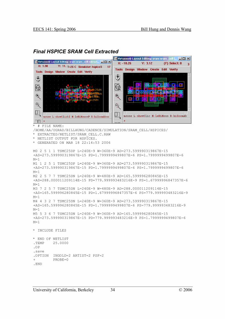
Final HSPICE SRAM Cell Extracted
* # FILE NAME: /HOME/AA/UGRAD/BILLHUNG/CADENCE/SIMULATION/SRAM_CELL/HSPICES/ * EXTRACTED/NETLIST/SRAM_CELL.C.RAW * NETLIST OUTPUT FOR HSPICES. * GENERATED ON MAR 18 22:14:53 2006 M0 2 5 1 1 TSMC25DP L=240E-9 W=360E-9 AD=273.599990319867E-15 +AS=273.599990319867E-15 PD=1.7999999499807E-6 PS=1.7999999499807E-6 M=1 M1 1 2 5 1 TSMC25DP L=240E-9 W=360E-9 AD=273.599990319867E-15 +AS=273.599990319867E-15 PD=1.7999999499807E-6 PS=1.7999999499807E-6 M=1 M2 2 5 7 7 TSMC25DN L=240E-9 W=480E-9 AD=165.599996280845E-15 +AS=288.000011209114E-15 PD=779.999993483216E-9 PS=1.67999996847357E-6 M=1 M3 7 2 5 7 TSMC25DN L=240E-9 W=480E-9 AD=288.000011209114E-15 +AS=165.599996280845E-15 PD=1.67999996847357E-6 PS=779.999993483216E-9 M=1 M4 4 3 2 7 TSMC25DN L=240E-9 W=360E-9 AD=273.599990319867E-15 +AS=165.599996280845E-15 PD=1.7999999499807E-6 PS=779.999993483216E-9 M=1 M5 5 3 6 7 TSMC25DN L=240E-9 W=360E-9 AD=165.599996280845E-15 +AS=273.599990319867E-15 PD=779.999993483216E-9 PS=1.7999999499807E-6 M=1 * INCLUDE FILES * END OF NETLIST .TEMP 25.0000 .OP .save .OPTION INGOLD=2 ARTIST=2 PSF=2 + PROBE=0 .END