Embed Size (px)
Citation preview
CadenceInteroperability Guide
Sponsored by
42 Cadence Interoperability Guide www.chipdesignmag.com/cadence
Cadence Interoperability Guide
Has there ever been a time when electronic tool interoperability
wasn’t a “big deal?” Be it chip or board development, it’s never been easy to get design data into the right format for one’s favorite simulation, analysis, or synthesis program. Either the data isn’t in the proper format to be input to a
particular software tool or the application-programming-interface (API) calls are all wrong. More often than not, design teams must spend a considerable amount of time reformatting data and tweaking interfaces in order to get all of the necessary EDA tools to work together. Such small tasks take time and money.
Even if many of the design tools are from a first-tier vendor, most design teams still need to connect these main flow tools to in-house specialty programs or optimized third-party tools. But achieving true interoperability takes time--time that could have been better spent achieving a design that meets the ever-shrinking time-to-market and cost pressures.
What can be done to enable tool interoperability? First, companies must agree to standards and open (non-proprietary) systems that enable multi-vendor, cross-platform development.
Standards for data file formats (e.g., GDSII) have been around for some time. Standards for a wider array of design and test data are finally gaining acceptance among both users and the EDA-vendor community. These data-repository standards, such as the original Cadence/Si2 OpenAccess database and API initiative, have paved the way for true interoperability. They provide a platform for an open design infrastructure.
The other key factor that encourages the OpenAccess movement is the need for a common platform for design data. Today’s chip designs are rich with variety--from analog and digital subsystems to multiple clock trees and varying power buses. The detailed design specification and interfaces for all of these different subsystems are contained in an unimaginably large array of data structures. Performing simulation and analysis on each of these subsystems requires tools that have access to a variety of data files and structures--all at the same time. The OpenAccess database provides data accessibility.
As powerful as it is, the OpenAccess database and API are only part of the total solution. Without an active community of users, no open system would succeed. Years ago, Cadence created its Connection Program to “promote open interoperability in all areas of electronic design including digital, custom IC, analog/mixed-signal and PCB design.” The goal of the program has been to attract best-in-class partners by offering an ever-growing collection of third-party solutions. These solutions operate fully with the Cadence suite of design tools.
To help customers incorporate the timeliest and most relevant point solutions into their design flow, Cadence provides a additional Connection Program category called Emerging Solution Members. To make these point solution tools available to their customers, Cadence jointly analyzes, develops, and optimizes the flow of data among the tools, while conducting technical and business development reviews to validate design flows. The result of this collaboration is an integrated product that customers can us to achieve interoperability. Some of the more recent Emerging Solution Members includes: CoWare,DFM, HELIC S.A., MatrixOne, Inc., Optimal Corporation, PDF Solutions Inc., Synplicity, Inc., and Valor Computerized Systems, Inc.
Collaboration of this sort is essential to the continued growth of innovative, second-tier startup companies. It also is needed to meet ever-tightening time-to-market demands. Programs that promote interoperability between EDA tool vendors, such as Cadence’s Connections Program, benefit vendors and users alike.
Connections Make Interoperability A Reality By John Blyler
43www.chipdesignmag.com/cadence Cadence Interoperability Guide
Cadence Interoperability Guide
The Cadence® Connections® program celebrates its 15th birthday, this year, and what a groundbreaking trip it’s
been. The first such effort of its kind back in 1992, Cadence Connections’ mission of encouraging openness in EDA has become standard procedure, now, in today’s EDA industry. But, at its inception, it was the epitome of forward thinking and innovation. And, 15 years later, Cadence Connections is still leading the way. Openness for its own sake is clearly a means to an important end, and that end is customer success.
From “accelerated layout” to “yield management,” Cadence Connections’ 137 members provide combined flows encompassed under 25 design-task categories. Through combined flows with these 137 members, Connections has given EDA users a vast expanse of choices. And, choice is crucial to customer success because no two electronic design projects are alike. The ability to combine the best of what the EDA industry has to offer, in ways that match specific design-project requirements, has shown itself, again and again, to be a critical success factor.
One customer recently wrote, “We are using Altos Design Automation Liberate with Cadence Virtuoso® Spectre® Circuit Simulator to generate electrical cell views for timing and power in Liberty format. Using Liberate, we are able to shorten the turnaround time to create new views or to update existing views to hours rather than days. We were also able to verify the run time scales almost linearly with the number of machines used. “The combination of Liberate and Spectre is only one example of openness tied directly to enhanced customer success.”
Another customer told us, “I am currently using Averant Inc.’s Solidify capability to export traces for failing assertions into the Cadence Incisive® functional verification environment. This allows my team to take advantage of both formal and dynamic verification technologies for efficient debugging. Having a tight integration between those tools increases the productivity of our verification team, which is key to the success of our projects.”
Cadence conceived of the Connections program in 1991, and by 1992 it was in full swing. In its first 15 years, it has grown to 137 members – the largest and most encompassing
of similar EDA programs. The Connections program is consistent with Cadence’s commitment to openness. After all, Cadence has donated and provided industry access to more than a dozen major proprietary languages, formats, API specifications and reference implementations. With Connections, members choose from three levels of connecting with Cadence tools: encapsulation, interfacing and integration. Encapsulation permits a member tool to launch from within the Cadence environment. Interfacing supports batch exchange of data. And, integration offers real-time, tool-to-tool interaction and communication.
Cadence makes it easy for third-party EDA vendors to take part in the Connections program. The process starts with an online application available on the Connections Web site (http://www.cadence.com/partners/connections/index.aspx). Member aspirants must have products already in the market, and customer requests for integration with Cadence tools. Upon joining, members receive Cadence software at minimal cost and take part in a comprehensive process for enabling the integration of their tools with those of Cadence.
Connections members span the design spectrum supporting the entire flow starting from ESL for architectural exploration through development and manufacturing. Verification tool, PCB software and custom IC tool vendors make up about 75 percent of Connections enabled flows, evenly split among the disciplines. The remaining 25 percent is a mix of ESL tools, digital IC physical design tools, physical verification tools, and DFM software.
Today’s electronic designs require degrees of specialty unknown in the early days of EDA. As IC technology has progressed to smaller features and denser circuitry, all facets of design and manufacturing have had to progress along with it, in lock step. Thus, no single EDA vendor can cover all the bases. The Cadence Connections program was developed to enable the collaboration of these specialties vendors to the ultimate benefit of their customers. From encapsulation through integration, each level of collaboration offers customers the benefits of compatibility, tape-out proven results, and better odds for successful designs.
Fifteen Years of Cadence Connections
44 Cadence Interoperability Guide www.chipdesignmag.com/cadence
Cadence Interoperability Guide
The entire EDA industry benefits from Connections by reducing redundancies and wheel reinvention and permitting the whole EDA process to progress through integrated contributions from Connections members. Members benefit because their products become part of holistic EDA solutions and are exposed to a broader base of potential customers. And, the ultimate winners are the customers who can tailor their design flows to the specifics of their design requirements without having to deal with incompatibilities and anomalies that slow them down and cost them more money.
Now, with 15 years under its belt, the Cadence Connections program is continuing to grow and fill out the 25 design-task categories. Even with the advent of open standards, open databases, and open API’s, which further enable interoperability, Connections membership continued to grow about 5 percent in 2006. Its diversity continues to reflect the diversity of EDA design, itself. And, customers continue to laud Connections benefits.
“Our IP Design Team continues to use Zenasis/Cadence flow to further improve design performance after taking it
through placement using SoC Encounter™,” writes one user. “The cells generated by Zenasis Technologies’ ZenTime are effectively used by Cadence SoC Encounter flow to give the best possible performance without penalizing area or power.”
Another user writes, “The Zenasis and Cadence flow is being used in our ARM 9-based flow to optimize design and this combined flow has given us performance gains in the range of 8 percent.”
This year, Connections celebrates its first 15 years. Fifteen years from now, designers will still be developing ICs and challenging the best minds in the EDA industry. And, Connections will continue to encourage the openness and collaboration that will provide those designers with best possible EDA flows.
46 Cadence Interoperability Guide www.chipdesignmag.com/cadence
Cadence Interoperability Guide
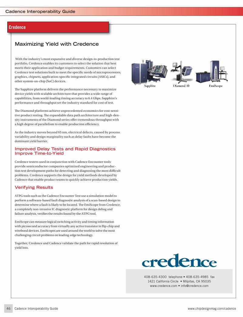
With the industry’s most expansive and diverse design-to-production test portfolio, Credence enables its customers to select the solution that best meets their application and budget requirements. Customers can select Credence test solutions built to meet the specifi c needs of microprocessors, graphics, chipsets, application-specifi c integrated circuits (ASICs), and other system-on-chip (SoC) devices.
Th e Sapphire platform delivers the performance necessary to maximize device yields with scalable architecture that provides a wide range of capabilities, from world-leading timing accuracy to 6.4 Gbps. Sapphire’s performance and throughput set the industry standard for cost of test.
Th e Diamond platforms achieve unprecedented economics for cost-sensi-tive product testing. Th e expandable data path architecture and high-den-sity instruments of the Diamond series off er tremendous throughput with a high degree of parallelism to enable production effi ciency.
As the industry moves beyond 65 nm, electrical defects, caused by process variability and design marginality such as delay faults have become the dominant yield barrier.
Improved Delay Tests and Rapid Diagnostics Improve Time-to-Yield
Credence testers used in conjunction with Cadence Encounter tools provide semiconductor companies optimized engineering and produc-tion test development paths for detecting and diagnosing the most diffi cult problems. Credence supports the design for yield methods developed by Cadence that enable product teams to quickly achieve production yields.
Verifying Results
ATPG tools such as the Cadence Encounter Test use a simulation model to perform a software-based fault diagnostic analysis of a scan-based design to determine where a fault is likely to be located. Th e EmiScope from Credence, a completely non-invasive IC diagnostic platform for design debug and failure analysis, verifi es the results found by the ATPG tool.
EmiScope can measure logical switching activity and timing information with picosecond accuracy from virtually any active transistor in fl ip-chip and wirebond devices. EmiScopes are used around the world to solve the most challenging circuit problems on leading-edge technology.
Together, Credence and Cadence validate the path for rapid resolution of yield loss.
Credence
408-635-4300 telephone • 408-635-4985 fax1421 California Circle • Milpitas, CA 95035
www.credence.com • [email protected]
Maximizing Yield with Credence
EDXACT
47www.chipdesignmag.com/cadence Cadence Interoperability Guide
Cadence Interoperability Guide
EdXact is an innovative EDA company dedicated to IC parasitic analysis and reduction. It has been created with the mission to help IC designers optimise post-layout simulation, maintain veri-fi cation accuracy and meet time-to-market goals. With IC designs targeting nanometer processes, backend verifi cation becomes a major bottleneck in the design cycle, which prevents designers to meet their time-to-market and time-to-volume targets. Th e overall goal of EdXact’s technology is to help reducing the number of re-spins that are necessary today to produce complex ICs.
Effi cient parasitic modelling is the key
EdXact’s team has a strong background in physical verifi cation, sig-nal integrity analysis, substrate and interconnect analysis, delay and crosstalk modeling, as well as in parasitic extraction techniques. Th e company is headquartered in Grenoble, France, which reinforces its collaboration with R&D groups from Universities and Laboratories.
Today, EdXact is the leading provider of standalone Model-Order-Reduction technologies. It’s mathematically proven algorithms are among the fi rst in the market to be able to handle mutual inductors and cross-coupling capacitors without compromising the accuracy of the underlying model. Th e company’s patent-pending tech-niques dramatically accelerate backannoted simulations in very large designs, while achieving sign-off accuracy.
Seamless integration into your design fl ow
EdXact is a niche player, aiming at boosting existing tools and fl ows by an order of magnitude and adding innovation for very special topics.
EdXact’s tools are developed to integrate within your existing fl ows. Close cooperation allows the combined tools to be com-pletely interoperable and user-friendly. Th e seamless integration with your EDA software provides an optimized and validated fl ow that is faster, much more effi cient and still accurate in order to meet sign-off requirements.
Boosting your existing tools
EdXact sells to IC and SOC designers inside fabs, IP providers and design houses.
EdXact’s products have already been selected by companies based in Europe, in the USA and in Japan. Th ey have been successfully used for circuits with integrated spiral inductors, analog-digital converters, VCOs, LDOs, power amplifi ers, as well as with very dense memory ICs, imaging ICs, microprocessors and many oth-ers. Customers are impressed by the speed improvements that are achieved, and very pleased to be able to use their simulation tools for new designs that otherwise would have been much too large.
SolutionsJivaro
Jivaro is a parasitic elements reduction platform that enables the speed up of physical design analysis tools by applying reduction
techniques while keeping results accuracy. It is composed of a large set of classic or innovative patent pending model order reduc-tion algorithms, and of a proprietary numerical data base allowing multi-threaded and distributed computations.
Based on this platform, EDXACT has developed 2 diff erent reduc-tion tools JivaroD and JivaroA , as well as an interconnections analysis tool Comanche. As major benefi ts, the reduction tools allow a number of simulation runs in the same time budget, with a preserved accuracy, thus improving the chances for a successful tape-out on time. Th e simulation time for larger designs turns from infi nite into hours, see minutes, and disk and memory require-ments for simulation tools decrease substantially.
Users can also apply diff erent degrees of reduction on diff erent parts of the design, from absolute accuracy preservation down to very aggressive reduction rate. Th ey naturally integrate in between the parasitic extractors and the physical verifi cation tools
JivaroD is a high volume parasitic networks reduction tool that performs the reduction of R, RC, RC lumped and RC coupled net-works. It can handle parasitic fi les of many gigabytes. It supports the DSPF and SPEF formats.
JivaroA is an analog/mixed-signal extracted circuits reduction tool that performs the reduction of R, RC, RCC, RLC and RLCK circuits and can handle fi les of a few gigabytes. It supports the SPECTRE and HSPICE post extraction formats. It is integrated in the Cadence Virtuoso and analog Artist platforms.
Comanche
Comanche is an accurate interconnections analysis tool that can be used within the physical verifi cation fl ow as a sanity check to detect “gross” violations before going into time consuming physical analyses.
Comanche features extremely fast resistance, S,Y,Z, parameters and Elmore delay calculation capabilities and can detect a bunch of problems such as opens and shortcuts, risk of IR drop, insuf-fi cient via insertion, unbalanced interconnections carrying diff er-ential signals, I/O inadequacies for RF circuits, and many others.
EDXACT
33-4-76-66-89-81 telephone • 33-4-76-67-36-99 faxRoute des Bpoise 38500 Voiron France
EDXACT: BRINGING INNOVATION INTO THE VERIFICATION FLOW
48 Cadence Interoperability Guide www.chipdesignmag.com/cadence
Cadence Interoperability Guide
ENOVIA MatrixOne’s DesignSync DFII
ENOVIA MatrixOne is pleased to announce important new capabilities in our semiconductor solution portfolio
Your design team used to be in a single department — today it’s often global. Yelling down the hallway once suffi ced for collaboration, but now communication must cross borders, languages and time zones. At one time you could survive with little or no design management in the fi nal stages of chip development — not any more.
As the complexity facing design teams has grown, so has their need for col-laboration and management for the backend of the design process. ENO-VIA MatrixOne provides that solution with the DesignSync DFII, which adds Cadence data recognition and processing to the standard DesignSync Design Data Management (DDM) solution, and an integration into the Cadence graphical design environment.
Th e DesignSync DFII is an integration into the Cadence Custom IC tool
user interface and is aware of the unique fi le system behaviors of the Ca-
dence software.
DesignSync can manage the immense amounts of information generated
from large design teams with hundreds of users. It has special features,
such as data caching and mirroring, to maintain performance across
multiple sites, while ensuring security with LDAP access control and SSL
encryption. Detailed information on the base platform is included in the
DesignSync datasheet.
Synchronicity DesignSyncDFII from Enovia MatrixOne is the clear industry leader for the Cadence IC community. With thousands of users across the wid-est customer base in the Semiconductor community, IC development teams have been succesfully reaping the benefi ts of design collaboration, IP reuse and library development and distribution as a seemless part of their design fl ow. Synchronicity DesignSyncDFII from Enovia MatrixOne is able to manage all kinds of data within one project and is the clear, proven choice for IC design teams and Semiconductor product companies.
Enovia MatrixOne
Les AlgorithmesBat Aristote A
2000 Routes des Lucioles 06901 Sophia Antipolis Cedex France
Moore’s law continues to drive both chip complexity and performance to new highs every year, and continues to stress and periodically “break” ex-isting design fl ows, such as functional verifi cation, traditionally the largest bottleneck in the design process.
Testing new devices like 3G cell phones, internet routers, image processors, etc. with complexity of hundreds of million transistors requires massive verifi cation sequences that would take many CPUyears to simulate on even the fastest PC. Increasingly, embedded software is overtaking the hardware content of SoC devices pushing processing needs to trillions of clock cycles. To harness the escalating problem, hardware-assisted verifi cation tools such as emulators and FPGA prototypes have been used for several years, but each suff ers its own set of drawbacks. Best-in-class emulation systems off er the large capacity required to emulate complex systems, good hardware debugging features and fairly ease setup. However they are very expensive assets, while their performance is just mediocre - often 500kHz or less. FPGA-based rapid prototyping systems can reach into tens of MHz and are much less costly than emulators. However, they typically accommodate small to medium designs of few million gates, require long setup times, and are not well suited to hardware debugging tasks.
EVE has pioneered an entirely new approach to hardware-assisted verifi ca-tion that combines the unique aspects of best-in-class emulators and rapid prototyping systems into a single, unifi ed environment for both ASIC/SoC debugging and embedded software validation.
With the high capacity, easy setup and debugging associated with emula-tion, and the price/performance of rapid prototyping, ZeBu (for Zero-Bugs) is ideal for block-level verifi cation and for the system-integration phase of the design cycle where multiple logic blocks and embedded software all must be verifi ed together. Hardware design and software development teams can share the same system and design representation, and can eas-ily collaborate when debugging complex hardware/software interactions.
Th e net eff ect is that hardware/software integration takes place much earlier in the design cycle, thereby reducing silicon respins and accelerat-ing time to market.
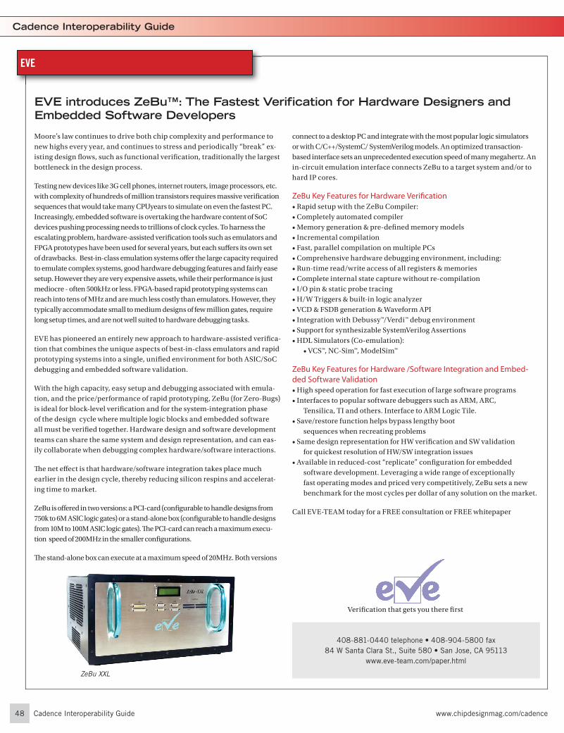
ZeBu is off ered in two versions: a PCI-card (confi gurable to handle designs from 750k to 6M ASIC logic gates) or a stand-alone box (confi gurable to handle designs from 10M to 100M ASIC logic gates). Th e PCI-card can reach a maximum execu-tion speed of 200MHz in the smaller confi gurations.
Th e stand-alone box can execute at a maximum speed of 20MHz. Both versions
connect to a desktop PC and integrate with the most popular logic simulators or with C/C++/SystemC/ SystemVerilog models. An optimized transaction-based interface sets an unprecedented execution speed of many megahertz. An in-circuit emulation interface connects ZeBu to a target system and/or to hard IP cores.
ZeBu Key Features for Hardware Verifi cation• Rapid setup with the ZeBu Compiler:• Completely automated compiler• Memory generation & pre-defi ned memory models• Incremental compilation• Fast, parallel compilation on multiple PCs• Comprehensive hardware debugging environment, including:• Run-time read/write access of all registers & memories• Complete internal state capture without re-compilation• I/O pin & static probe tracing• H/W Triggers & built-in logic analyzer• VCD & FSDB generation & Waveform API• Integration with Debussy™/Verdi™ debug environment• Support for synthesizable SystemVerilog Assertions• HDL Simulators (Co-emulation): • VCS™, NC-Sim™, ModelSim™
ZeBu Key Features for Hardware /Software Integration and Embed-ded Software Validation• High speed operation for fast execution of large software programs• Interfaces to popular software debuggers such as ARM, ARC,
Tensilica, TI and others. Interface to ARM Logic Tile.• Save/restore function helps bypass lengthy boot
sequences when recreating problems• Same design representation for HW verifi cation and SW validation
for quickest resolution of HW/SW integration issues• Available in reduced-cost “replicate” confi guration for embedded
software development. Leveraging a wide range of exceptionally fast operating modes and priced very competitively, ZeBu sets a new benchmark for the most cycles per dollar of any solution on the market.
Call EVE-TEAM today for a FREE consultation or FREE whitepaper
EVE
408-881-0440 telephone • 408-904-5800 fax84 W Santa Clara St., Suite 580 • San Jose, CA 95113
www.eve-team.com/paper.html
ZeBu XXL
EVE introduces ZeBu™: The Fastest Verifi cation for Hardware Designers and Embedded Software Developers
Verifi cation that gets you there fi rst
49www.chipdesignmag.com/cadence Cadence Interoperability Guide
Cadence Interoperability Guide
ENOVIA MatrixOne’s DesignSync DFII
ENOVIA MatrixOne is pleased to announce important new capabilities in our semiconductor solution portfolio
Your design team used to be in a single department — today it’s often global. Yelling down the hallway once suffi ced for collaboration, but now communication must cross borders, languages and time zones. At one time you could survive with little or no design management in the fi nal stages of chip development — not any more.
As the complexity facing design teams has grown, so has their need for col-laboration and management for the backend of the design process. ENO-VIA MatrixOne provides that solution with the DesignSync DFII, which adds Cadence data recognition and processing to the standard DesignSync Design Data Management (DDM) solution, and an integration into the Cadence graphical design environment.
Th e DesignSync DFII is an integration into the Cadence Custom IC tool
user interface and is aware of the unique fi le system behaviors of the Ca-
dence software.
DesignSync can manage the immense amounts of information generated
from large design teams with hundreds of users. It has special features,
such as data caching and mirroring, to maintain performance across
multiple sites, while ensuring security with LDAP access control and SSL
encryption. Detailed information on the base platform is included in the
DesignSync datasheet.
Synchronicity DesignSyncDFII from Enovia MatrixOne is the clear industry leader for the Cadence IC community. With thousands of users across the wid-est customer base in the Semiconductor community, IC development teams have been succesfully reaping the benefi ts of design collaboration, IP reuse and library development and distribution as a seemless part of their design fl ow. Synchronicity DesignSyncDFII from Enovia MatrixOne is able to manage all kinds of data within one project and is the clear, proven choice for IC design teams and Semiconductor product companies.
Enovia MatrixOne
Les AlgorithmesBat Aristote A
2000 Routes des Lucioles 06901 Sophia Antipolis Cedex France

51www.chipdesignmag.com/cadence Cadence Interoperability Guide
Cadence Interoperability Guide
SPICE Explorer • Transistor-level debugging environment off ering pre-sim
SPICE-centric productivity resources, netlist debugging and extensive post-sim waveform analysis/reporting capabilities
WaveView Analyzer • Post-sim high-performance analog / mixed-signal waveform analyzer
Analysis Command Environment (ACE) • Tcl and Perl-driven APIs for customization
DT • Support for oscilloscope, IBIS and Liberty® .Lib formats
SX Link • Framework integration -- schematic cross-
probing from Cadence Virtuoso SE and ADE, Mentor Graphics Design Architect IC environments
SX Link ENS • Cadence Virtuoso SE and ADE extracted netlist
simulation cross-probing to ideal schematic
ChipView • Post-layout RC-extraction simulation results visualization
SpiceCheck • Static netlist-driven programmable design checker
Sandwork Design, Inc.
650-988-9934x120 telephone • 650-988-9935 fax1451 Grant Road, #104 • Mountain View, CA 94040
www.sandwork.com
Sandwork Design’s AVAD Suites (Analysis Verifi cation And Debugging) offer universal waveform analysis and static netlist checking tools that deliver support for analysis of data from all four areas of IC/PCB SI simulation, scope measurement, circut modeling and full-chip verifi cation
Sandwork tools greatly enhance design fl ows, interfacing with signal integrity, analog and mixed-signal simulators from Cadence, Synopsys, Nacentric and Mentor. Sandwork’s robust solution speed up the many critical tasks during simulation verifi cation, allowing customers to shorten design cycles, facilitate cross-team reviews and improve chip performance.
52 Cadence Interoperability Guide www.chipdesignmag.com/cadence
Cadence Interoperability Guide
Synplify Premier with Graph-based Physical Synthesis
Synplify® Premier software builds upon Synplicity’s industry-leading tech-nology and adds new graph-based physical synthesis for timing closure and simulator-like visibility into operating FPGA devices for fast source-level debugging.
Invented by Synplicity, graph-based physical synthesis improves timing closure by means of a single-pass physical synthesis fl ow for 90nm FPGAs. Unlike ASICs, proximity does not imply better timing in FPGAs. In graph-based physical synthesis, pre-existing wires, switches, and placement sites used for routing an FPGA can be represented as a detailed routing resource graph. Th e notion of distance then changes to a measure of delay and availability of wires. Th e Synplify Premier solution’s graph-based physical synthesis technology merges optimization, placement, and routing to generate a fully placed and physically optimized netlist, providing rapid timing closure and a 5 - 20% timing improvement.
Th e Synplify Premier solution quickly fi nds functional errors in FPGA de-signs by providing simulator-like visibility into operating FPGA hardware. Based upon technology from the Identify® product, the Synplify Premier tool has integrated debugging software that allows designers to annotate signals and conditions they want to monitor directly in their RTL code. Once the FPGA has been programmed, the RTL debugger is run, allow-
ing users to view actual signal values from a running FPGA directly in their RTL code and debug it, in-system, and at the target operating speed. Advanced triggering helps pinpoint design problems.
With the addition of graph-based physical synthesis and source-level, in-circuit debugging to the world’s best FPGA synthesis technology, the Synplify Premier product is the industry’s most comprehensive and pro-ductive FPGA design solution.
For FPGA users that are prototyping an ASIC, the Synplify Premier software accepts inputs that are compatible with industry-leading ASIC synthesis tools, allowing you to quickly retarget your FPGA prototype design to an ASIC. Compatibility features includes support for basic Designware compo-nents, automatic gated clock conversion, and the use of SDC constraints.
Synplicity, Inc.
408-215-6000 telephone • 408-222-0268 fax600 W. California Ave
Sunnyvale, CA 94086 USAwww.synplicity.com • [email protected]
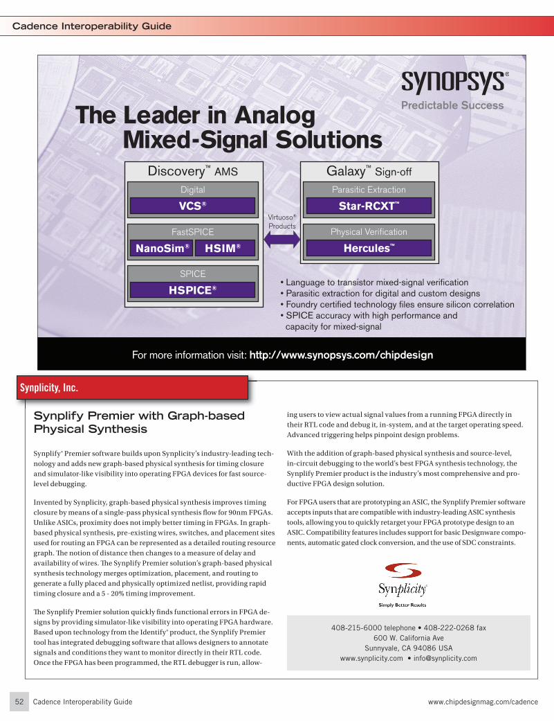
The Leader in Analog Mixed-Signal Solutions
For more information visit: http://www.synopsys.com/chipdesign
FastSPICE
Discovery™ AMS
VCS®
Digital
HSPICE®
SPICE
NanoSim® HSIM®
Galaxy™ Sign-off
Star-RCXT™
Parasitic Extraction
Hercules™
Physical Verification
Virtuoso®
Products
• Language to transistor mixed-signal verification• Parasitic extraction for digital and custom designs • Foundry certified technology files ensure silicon correlation• SPICE accuracy with high performance and capacity for mixed-signal
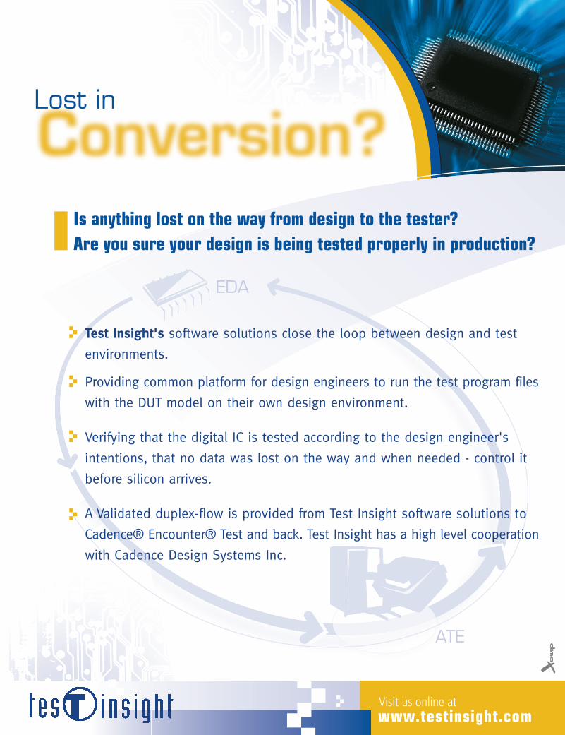
Is anything lost on the way from design to the tester?Are you sure your design is being tested properly in production?
www.testinsight.comVisit us online at
EDA
ATE
Lost in
Test Insight's software solutions close the loop between design and test
environments.
Providing common platform for design engineers to run the test program files
with the DUT model on their own design environment.
Verifying that the digital IC is tested according to the design engineer's
intentions, that no data was lost on the way and when needed - control it
before silicon arrives.
A Validated duplex-flow is provided from Test Insight software solutions to
Cadence® Encounter® Test and back. Test Insight has a high level cooperation
with Cadence Design Systems Inc.
54 Cadence Interoperability Guide www.chipdesignmag.com/cadence
Cadence Interoperability Guide
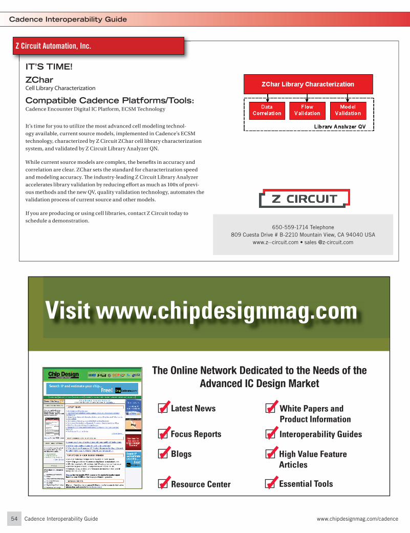
IT’S TIME!
ZCharCell Library Characterization
Compatible Cadence Platforms/Tools: Cadence Encounter Digital IC Platform, ECSM Technology
It’s time for you to utilize the most advanced cell modeling technol-ogy available, current source models, implemented in Cadence’s ECSM technology, characterized by Z Circuit ZChar cell library characterization system, and validated by Z Circuit Library Analyzer QN.
While current source models are complex, the benefi ts in accuracy and correlation are clear. ZChar sets the standard for characterization speed and modeling accuracy. Th e industry-leading Z Circuit Library Analyzer accelerates library validation by reducing eff ort as much as 100x of previ-ous methods and the new QV, quality validation technology, automates the validation process of current source and other models.
If you are producing or using cell libraries, contact Z Circuit today to schedule a demonstration.
Z Circuit Automation, Inc.
650-559-1714 Telephone809 Cuesta Drive # B-2210 Mountain View, CA 94040 USA
www.z--circuit.com • sales @z-circuit.com
The Online Network Dedicated to the Needs of the Advanced IC Design Market
Visit www.chipdesignmag.com
Latest News
Focus Reports
Blogs
White Papers andProduct Information
Interoperability Guides
High Value Feature Articles
Resource Center Essential Tools