Embed Size (px)
Citation preview
1
4 November 2008 1
CAD Algorithms
Placement
Mohammad Tehranipoor
ECE Department
4 November 2008 2
Placement and Floorplanning
� Layout maps the structural representation of circuit into a
physical representation
� Physical representation:
� Geometric coordinates for all the circuit elements and the
wiring that interconnects the elements
� A circuit is represented by:
� list of circuit elements
� list of signals (nets) indicating terminals to be connected
together
2
4 November 2008 3
Important Features
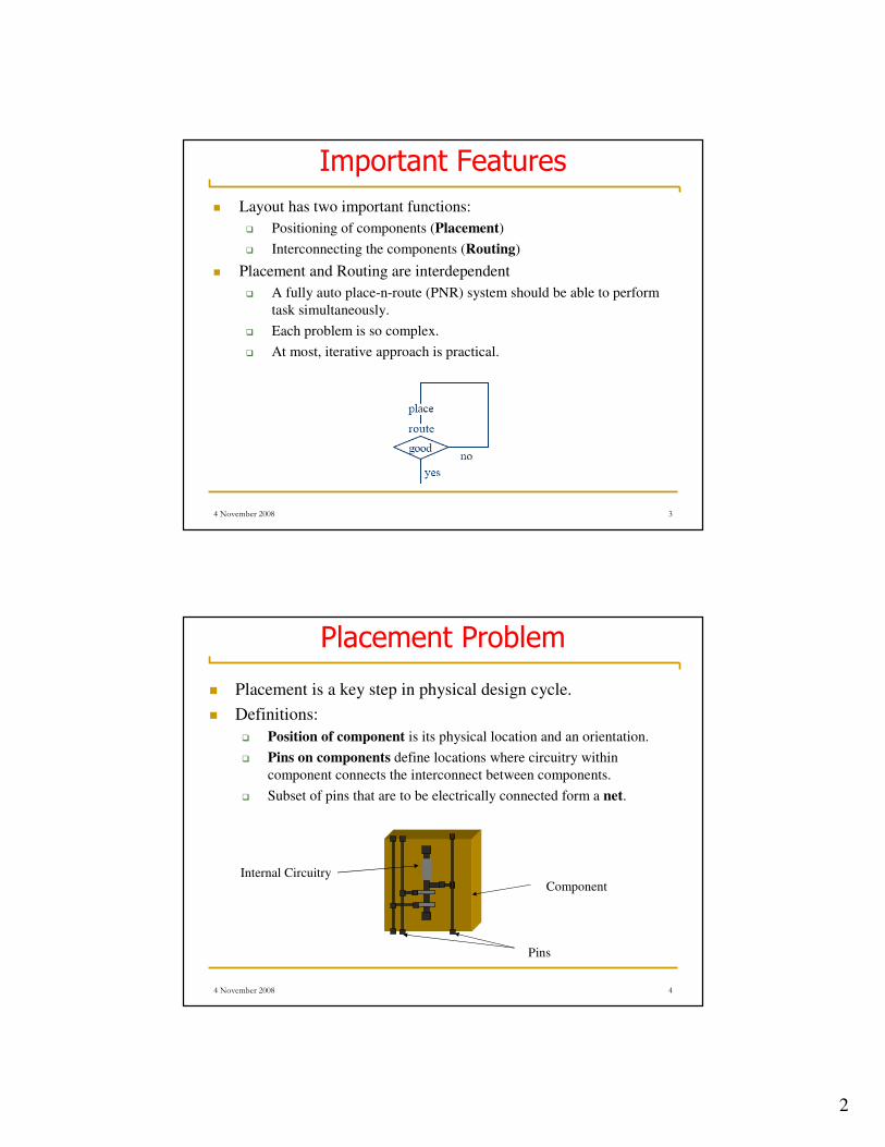
� Layout has two important functions:
� Positioning of components (Placement)
� Interconnecting the components (Routing)
� Placement and Routing are interdependent
� A fully auto place-n-route (PNR) system should be able to perform
task simultaneously.
� Each problem is so complex.
� At most, iterative approach is practical.
4 November 2008 4
Placement Problem
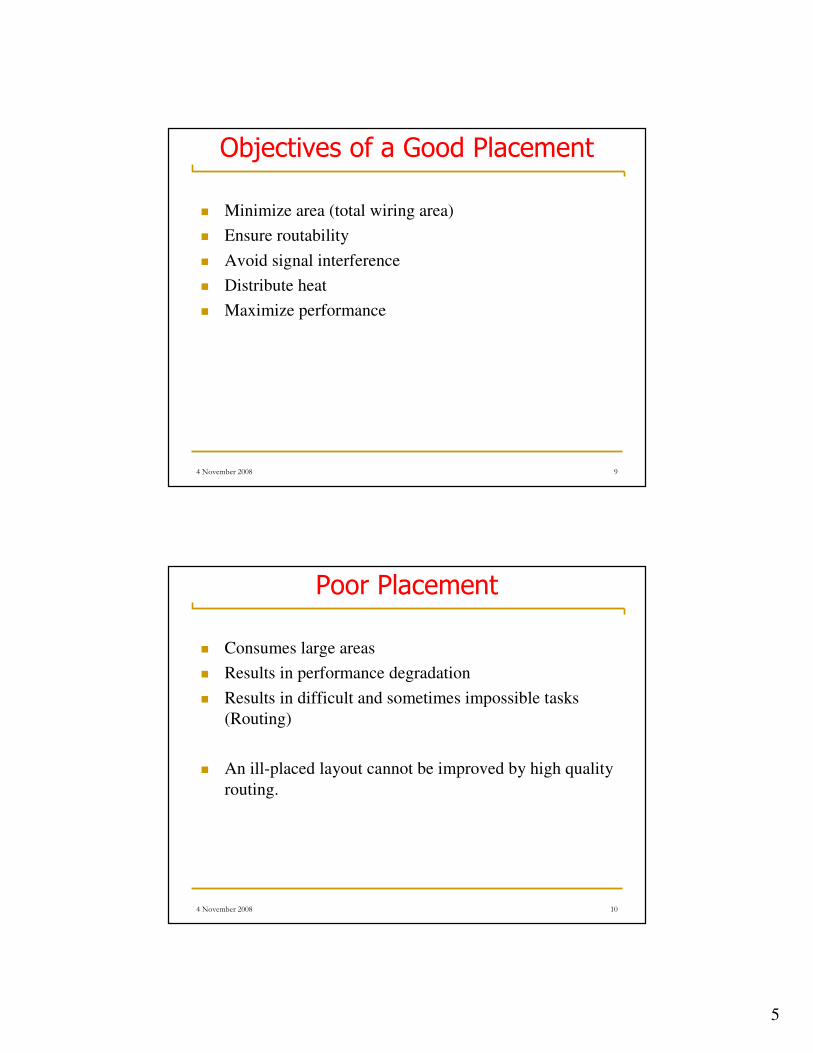
� Placement is a key step in physical design cycle.
� Definitions:
� Position of component is its physical location and an orientation.
� Pins on components define locations where circuitry within
component connects the interconnect between components.
� Subset of pins that are to be electrically connected form a net.
ComponentInternal Circuitry
Pins

3
4 November 2008 5
Placement Problem
� Depending on the IC design style Placement has
different goals:
� Placement can affect Router
� Placement should concentrate on minimizing the length of
interconnection or area
� Delays and design performance greatly depend on placement
4 November 2008 6
Input/Output of Placement
� Input:
� Set of fixed blocks
� Number and location of terminals for each block
� Netlist
� Block’s dimensions
� Output
� Exact location of blocks
� Location of pins assigned to each component

4
4 November 2008 7
Placement at Various Levels
� System Level:
� Place all the PCBs together so that
� The area occupied is minimum.
� Heat is dissipated properly.
� Board Level:� All the chips must be placed within a fixed area of the PCB.
� All blocks are fixed and rectangular/square in shape.
� Some chips may be pre-placed
� Minimize routing layers
� Heat dissipation
� Chip Level:� Limited number of layers
� Minimum area
� Performance
4 November 2008 8
Objectives
� Normally we are given the maximum chip area
� Placement should define locations such that
� All elements get connected (routability)
� Routing area is minimized
� Routability and Performance are the measures of good Placement
� Routability:� Depends on number of factors such as Router being used.
� Minimum routing area can only be estimated
� Performance:
� Depends on wirelengths.
5
4 November 2008 9
Objectives of a Good Placement
� Minimize area (total wiring area)
� Ensure routability
� Avoid signal interference
� Distribute heat
� Maximize performance
4 November 2008 10
Poor Placement
� Consumes large areas
� Results in performance degradation
� Results in difficult and sometimes impossible tasks
(Routing)
� An ill-placed layout cannot be improved by high quality
routing.

6
4 November 2008 11
Placement Methodology
Goals:
Time, Performance, …
Minimize Wirelength,
Maximize Routability
Placement
� Assume ds = total wirelength estimated for each net
� ∑ di = Nd = total estimated wirelength of the layout
� Objective:
� Place such that Nd is to be minimized
allnets
4 November 2008 12
Placement Problem Formulation
� Given an electrical circuit consisting of fixed blocks and
a netlist interconnecting terminals on the periphery of
these blocks
� Let B1, B2, …,Bn be the blocks to be placed.
� Each Bi, 1 ≤ i ≤ n, has hi and wi.
� Let N = {N1, N2, …,Nm} be the set of nets.
� Let Q = {Q1, Q2, …, Qk} be the rectangular empty areas allocated for routing between the blocks.
� Let Li denote the estimated length of net Ni, 1 ≤ i ≤ m.
7
4 November 2008 13
Cont.
� Construct a layout indicating the positions of each block
such that:
� No two rectangles overlap
� Placement is routable
� The total area of bounding box is minimized
� The total estimated wirelength is minimized
� In the case of high performance circuits
� The length of longest net is also minimized. This problem is
known as the performance driven placement problem.
� The algorithm must ensure that the known critical paths lengths
are shorter than a predefined value.
� Placement problem is NP-complete.
4 November 2008 14
Topological Congestion
� The layout area and routability of the layout
are approximated by topological congestion.
Less Congestion

8
4 November 2008 15
Wirelength
� The actual wiring paths are not known at the time of
placement.
� Minimum spanning tree representations are the most
commonly used structures to connect a net in the
placement phase.
� MST is also used in Global routing phase.
� Optimal wiring paths for a net can be obtained using
Rectilinear Steiner Tree.
� RST is used in detailed routing phase.
4 November 2008 16
Design Style Specific Placement
� Different design styles impose different restrictions on the
layout and have different objectives in placement problems.
� Full Custom:
� No restriction on how the blocks can be placed.
� No two blocks overlap.
� Minimize the total layout area.
� The irregularity of block shapes is the main cause of unused
areas (dead space).
� Minimize the unused areas.
� The objective of minimizing the layout area sometimes
conflicts with the objective of minimizing the maximum
length of a net.
� In high performance circuit design, additional constraints on
net length are considered.
9
4 November 2008 17
Design Style Specific Placement
� Standard Cells:� Simpler than the full custom placement problem
� Cells have same height.
� Cells are placed in rows.
� Minimizing area is equivalent to minimizing the summation of channel heights and minimizing the width of the widest row.
� All rows usually have equal widths.� This may not be the case when using large standard cells.
� Total area:� Required area for cells
� Required area for channels
� With advent of over-the-cell routing, the channels in the standard cells have almost disappeared (channel-less standard cell designs).
� Same for metal layers
4 November 2008 18
Design Style Specific Placement
� Gate Array:
� We already have
� Logic prefabricated
� Limited routing area
� Placement tries to find mappings for circuit elements that
ensures routability in limited space
� Minimizing routing area is not as important as ensuring
routability by minimizing congestion
10
4 November 2008 19
Placement Algorithms
� Partitioning-Based Algorithms
� Simulation-Based Algorithms� Simulated Annealing
� Genetic Algorithm
� Performance-Driven Placement Algorithm
4 November 2008 20
Partitioning-Based Algorithms
Breuer’s Algorithms:
� The main idea for Breuer’s algorithm is to reduce the
number of nets being cut when the circuit is partitioned.
� Given
� E={e1,e2,…,en} a set of elements
� S={s1,s2,…,sm} a set of signals (nets)
� L={l1,l2,…,lp}, p ≥ n a set of locations
� Assign each element to unique location such that something is
minimized.
11
4 November 2008 21
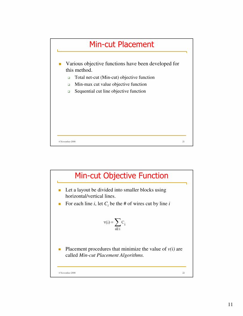
Min-cut Placement
� Various objective functions have been developed for
this method.
� Total net-cut (Min-cut) objective function
� Min-max cut value objective function
� Sequential cut line objective function
4 November 2008 22
Min-cut Objective Function
� Let a layout be divided into smaller blocks using
horizontal/vertical lines.
� For each line i, let Ci be the # of wires cut by line i
� Placement procedures that minimize the value of v(i) are
called Min-cut Placement Algorithms.
12
4 November 2008 23
Min-max Cut Value Objective Function
� In case of standard cells and gate arrays, the channel
width depends on the number of nets that are routed
through the channel.
� The more the number of nets the larger is the channel
width.
� The objective function is to reduce the number of nets cut
by the cut line across the channel.
� This will reduce the congestion in channels.
4 November 2008 24
Sequential Cut Line Objective Function
� It is very difficult to compute the minimum net cuts.
� Find cut lines c1, c2, c3,…cn in sequential manner
such that:
min(v(cn))| subject to
min(v(cn-1))| subject to
.
.
min(v(c1))
13
4 November 2008 25
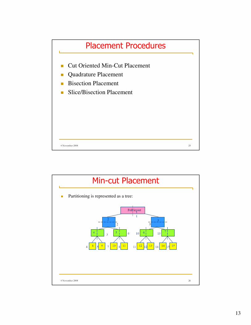
Placement Procedures
� Cut Oriented Min-Cut Placement
� Quadrature Placement
� Bisection Placement
� Slice/Bisection Placement
4 November 2008 26
Min-cut Placement
� Partitioning is represented as a tree:
14
4 November 2008 27
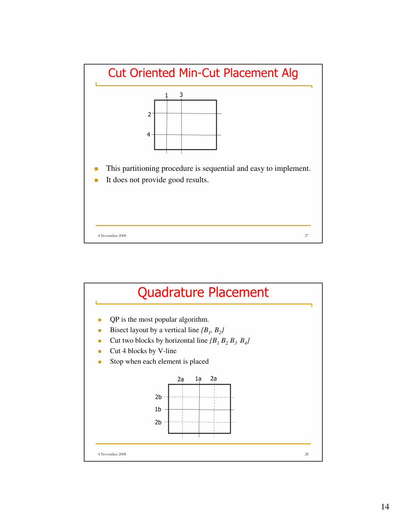
Cut Oriented Min-Cut Placement Alg
1
4
3
2
� This partitioning procedure is sequential and easy to implement.
� It does not provide good results.
4 November 2008 28
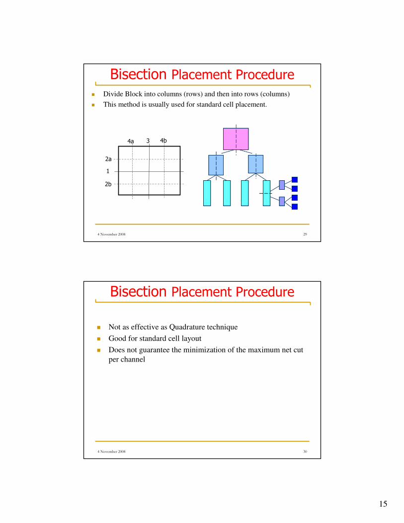
Quadrature Placement
� QP is the most popular algorithm.
� Bisect layout by a vertical line {B1, B2}
� Cut two blocks by horizontal line {B1 B2 B3 B4}
� Cut 4 blocks by V-line
� Stop when each element is placed
2a
2b
1a
1b
2a
2b
15
4 November 2008 29
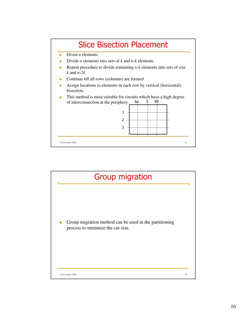
Bisection Placement Procedure� Divide Block into columns (rows) and then into rows (columns)
� This method is usually used for standard cell placement.
4a
2b
3
1
4b
2a
4 November 2008 30
Bisection Placement Procedure
� Not as effective as Quadrature technique
� Good for standard cell layout
� Does not guarantee the minimization of the maximum net cut
per channel
16
4 November 2008 31
Slice Bisection Placement� Given n elements
� Divide n elements into sets of k and n-k elements
� Repeat procedure to divide remaining n-k elements into sets of size
k and n-2k
� Continue till all rows (columns) are formed
� Assign locations to elements in each row by vertical (horizontal)
bisection.
� This method is most suitable for circuits which have a high degree
of interconnection at the periphery. 6a
3
5
2
6b
1
4 November 2008 32
Group migration
� Group migration method can be used in the partitioning
process to minimize the cut size.
17
4 November 2008 33
Simulated Annealing
4 November 2008 34
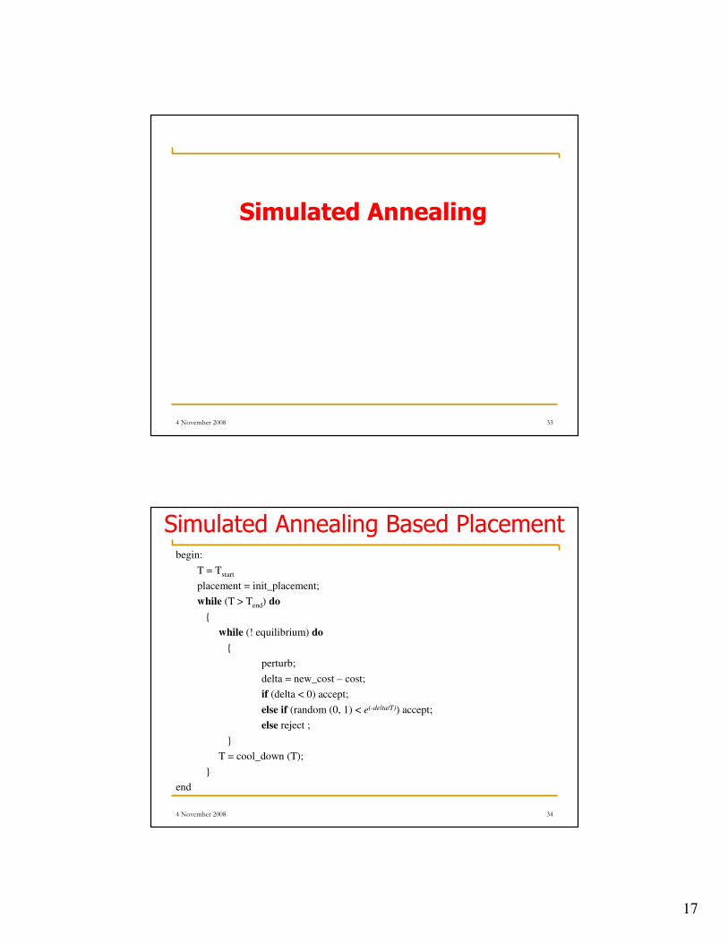
Simulated Annealing Based Placementbegin:
T = Tstart
placement = init_placement;
while (T > Tend) do
{
while (! equilibrium) do
{
perturb;
delta = new_cost – cost;
if (delta < 0) accept;
else if (random (0, 1) < e(-delta/T)) accept;
else reject ;
}
T = cool_down (T);
}
end

18
4 November 2008 35
TimberWolf 3.2
� TimberWolf is a standard cell placement algorithm based
on Simulated Annealing.
� TimberWolf is one of the most successful placement
algorithm.
� In this algorithm, the parameters and functions are taken
as follows:
� Fixed schedule
� Tstart = 4,000,000 // Initial temperature
� Tend = 0.1 // Final temperature
� Cool_down = alpha (T) x T
� alpha (T) = 0.8 � 0.95 � 0.8
4 November 2008 36
TimberWolf 3.2 (Cont.)
� Perturb
� Displace a block to a new location
� Swap two blocks
� Change orientation of a block
� Cost function
Cost = α × wire length + β × block overlap + γ × row length overshoot
19
4 November 2008 37
Automatic Schedule
� Quality of placement depends on:
� Perturb
� Cost function
� Cooling schedule
� Runtime of SA placement depends on:
� Annealing (cooling) schedule
� Quality Vs Runtime:
� Non-linear/complex relationship
4 November 2008 38
Perturb
� Displace the current solution as little as possible
� Swaps, moves and reorients are widely used
� Affecting too many blocks will not work
� Temperature dependant Range limiters
� At High T, use the entire device
� As T lowers, use a smaller window of the device for
swap/move targets
20
4 November 2008 39
Tweak Zones
� Cost function
� Components, weights
� Perturb
� Range limiters, moves/swaps etc
� Equilibrium
� Tend
4 November 2008 40
Genetic Algorithm

21
4 November 2008 41
Genetic Algorithm
� Initial set of placement configurations is called Population, which
can be generated randomly.
� The individuals in the population represent a feasible placement.
� SCORE is same as fitness.
� It can be wirelength.
� Three operations:
� Crossover
� Mutation
� Selection
4 November 2008 42
Genetic Algorithmbegin
no_pop = SIZE-POP;
no_offspring = no_pop X k;
pop = CONSTRUCT-POP(no-pop);
for (i = 1 to no_pop) do
SCORE(pop(i))
for (i = 1 to no_generation) do
for (j = 1 to no_offspring) do
(x,y) = CHOOSE-PARENT(pop)
offspring(j) = GENERATE(x,y);
SCORE(offspring(j));
pop = SELECT(pop, offspring, no_pop);
for (j = 1 to no_pop) do
MUTATE(pop(j));
Return highest scoring configuration in population
end.
22
4 November 2008 43
Performance Driven Placement
� The delay at chip level plays an important role in determining
performance of the chip.
� As the number of blocks in a chip increases, the size of the
chip decreases but may result in longer interconnections
between the blocks (performance degradation).
� The placement algorithms for high performance chips have to
generate placements which will allow routers to route nets
within the timing requirements.
� Also called path-based approach.
� The critical path length must be within its timing constraint.