Embed Size (px)
Citation preview

C5535 DSPShield H/W Reference Manual
Version 0.1
In Collaboration with Stanford University
page i
C5535 DSPSHIELD
Hardware Reference Manual
H/W Rev. A

C5535 DSPShield H/W Reference Manual
Version 0.1
In Collaboration with Stanford University
page ii
Revision History
Version Date Author Notes 0.1 Aug 12, 2013 D. Garcia 1
NOTES:
1. Initial release. 2.

C5535 DSPShield H/W Reference Manual
Version 0.1
In Collaboration with Stanford University
page iii
Table of Contents
1� C5535 DSPShield ...................................................................................................... 1�1.1� Key Features ...............................................................................................................1�1.2� DSPShield Architecture..............................................................................................2�1.3� User Control Elements ...............................................................................................3�1.4� DSPShield Application Photos ...................................................................................4�2� Power Management .................................................................................................. 4�2.1� External Power Interface ............................................................................................4�2.2� Internal Voltages ........................................................................................................6�2.3� Voltage Monitoring ....................................................................................................6�2.4� C5535 DSP Core Voltage ...........................................................................................7�3� C5535 DSP and Internal Peripherals ...................................................................... 7�3.1� Parallel and Serial Peripherals ....................................................................................7�3.2� Clock Sources .............................................................................................................8�3.3� ROM Bootloader ........................................................................................................9�3.4� /INT1, /INT0, XF, WAKEUP ..................................................................................10�3.5� USB Controller .........................................................................................................10�3.6� MMC/SDx Controller ...............................................................................................10�3.7� I2C ............................................................................................................................10�4� DSPShield Peripherals............................................................................................ 11�4.1� I2C GPIO Expander .................................................................................................11�4.2� OLED Display ..........................................................................................................14�4.3� TLV320ACI3204 Audio Codec ...............................................................................14�4.4� Micro SD Card Connector ........................................................................................14�4.5� DIP Switch Inputs, LEDs and Push Button Reset ....................................................14�4.6� DSP Expansion Connector .......................................................................................15�5� Emulation................................................................................................................. 16�5.1� FTDI FT2232H .........................................................................................................16�5.2� Power via XDS-USB ................................................................................................17�6� Arduino Interface .................................................................................................... 17�6.1� Arduino/DSPShield Interface Block Diagram .........................................................19�6.1.1� Interface Logic Levels ............................................................................... 19�6.1.2� Analog Inputs ............................................................................................ 20�6.2� Arduino/DSPShield Reset Multiplexing ..................................................................20�

C5535 DSPShield H/W Reference Manual
Version 0.1
In Collaboration with Stanford University
page iv
6.2.1� Default Configuration ................................................................................ 22�6.2.2� C5535 Isolated from ARD_RESETN pin ................................................. 23�6.2.3� C5535 Resets Arduino ............................................................................... 23�6.2.4� C5535 Self Resets ...................................................................................... 23�6.2.5� Emulator Only Resets the DSPShield ....................................................... 23�6.3� DSPShield UART Multiplexing ...............................................................................23�6.3.1� DSP Expansion Connector ........................................................................ 25�6.3.2� Arduino IO[1:0] ......................................................................................... 25�6.3.3� Emulator Serial Port .................................................................................. 25�6.4� Arduino/DSPShield I2C Interface ............................................................................26�6.5� Arduino SPI Interface ...............................................................................................26�6.5.1� Arduino Master/C5535 DSP Isolated ........................................................ 27�6.5.2� Arduino Slave/C5535 DSP Master ............................................................ 28�6.5.3� Arduino Isolated/C5535 DSP Master ........................................................ 28�7� Resistor Multiplexing Configurations ................................................................... 28�8� Stand-Alone Mode .................................................................................................. 30�9� Assembly Drawings and Schematics ..................................................................... 31��
Reference documents
Title / source Owner Version
1 TMS320C5535 Data Sheet SPRS737B AUGUST 2011–REVISED MARCH 2012 TI
2 TMX320C5535 Technical Reference Manual SPRUH87C August 2011–Revised March 2012 TI
3 TLV320AIC3204 Ultra Low Power Stereo Audio Codec SLOS602B –SEPTEMBER 2008–REVISED OCTOBER 2012
TI
4 TCA6416A I2C to GPIO Expander SCPS194A – MAY 2009– REVISED NOVEMBER 2009
TI
5 Dual High Speed USB to Multipurpose UART/FIFO IC http://www.ftdichip.com/Support/Documents/DataSheets/ICs/DS_FT2232H.pdf
FTDI
6 Arduino UNO Information http://arduino.cc/en/Main/ArduinoBoardUno
Arduino
7 OLED Display OSD9616P0992-10 http://osddisplays.com/
OSD Display

C5535 DSPShield H/W Reference Manual
Version 0.1
In Collaboration with Stanford University
page v
Acronyms Abbreviations and Definitions
Arduino Family of Open Hardware uC Boards
Arduino UNO 2chip Arduino uC Board
Arduino Leonardo 1chip Arduino uC Board
CCS Code Composer Studio TI Emulation Software
DC-DC Switching regulator
DSP Digital Signal Processor
DNI Do Not Install
Energia Open Source software IDE for TI Processors
GPIO General Purpose Input Output
I2C Inter-Integrated Circuit (2-pin serial bus)
I2S Integrated Interchip Sound (4-pin serial bus for audio devices)
IDE Integrated Development Environment
LCD Liquid Crystal Display
LDO Low Drop-Out regulator
MMC/SD Multimedia Card/Secure Digital (flash memory)
OLED Organic Light Emitting Diode (Display)
UART Universal Asynchronous Receiver Transmitter (serial bus)
XDS Extended Development System. JTAG Emulators for TI Processors (embedded or external)

C5535 DSPShield H/W Reference Manual Version 0.1
In Collaboration with Stanford University
page 1
1 C5535 DSPShield The C5535 DSPShield is an evaluation board for the Texas Instruments TMS320C5535 Fixed-Point Digital Signal Processor (DSP). It is designed to be both a “Shield” (i.e. daughter card) for the Arduino Open-Hardware family of microcontroller (uC) boards and also a stand-alone development board. With a rich set of hardware features and a connector for prototyping expansion, the C5535 DSPShield can be used to develop applications such as
• Wireless Audio Devices (e.g., Headsets, Microphones, Speakerphones) • Echo Cancellation Headphones • Portable Medical Devices • Voice Applications • Industrial Controls • Fingerprint Biometrics • Software-defined Radio
1.1 Key Features The key features of the C5535 DSPShield are shown in Figure 1. The features include:
x TI TMS320C5535AZHHA10 (100MHz) Digital Signal Processor
x TI TLV320AIC3204IRGBR Stereo Audio Codec with separate stereo in and stereo out connectors
x Micro SD Card Connector
x USB 2.0 interface to the C5535 DSP
x OLED 96x16 pixel display
x Arduino Compatible Header Connectors
x Arduino Interface is compatible with Energia software IDE and API
x Embedded USB XDS100-V2 JTAG emulator with secondary serial port o JTAG is compatible with TI Code Composer Studio software IDE o Secondary serial port is compatible with Energia software IDE and API
x 40-pin DSP Expansion Connector
x 3 user controlled LEDs,
x 4 user readable DIP switches
x 1 hardware reset push button switch
x Flexible Power Sourcing

C5535 DSPShield H/W Reference Manual Version 0.1
In Collaboration with Stanford University
page 2
Figure 1. Key Features of the C5535 DSPShield
1.2 DSPShield Architecture The C5535 DSP is a peripheral rich processor. However, to limit the pin count, the C5535’s pins are heavily multiplexed. Depending on the application, the C5535 is programmed with the appropriate internal peripherals routed to its external pins. The DSPShield maintains this flexibility by using additional discrete multiplexers to connect the C5535’s GPIO/peripheral pins to the appropriate points on the board. Additonal flexibility can also be found in the power management for the board and in the Arduino/DSPShield interface. The DSPShield block diagram is shown in Figure 2. The DSPShield architecture consists of the following major blocks:
1. Power Management 2. The C5535 DSP and Internal Peripherals 3. DSPShield Peripherals 4. Arduino Interface 5. DSP Expansion Connector 6. XDS100-V2 Embedded Emulator

Figur
1.3 The uboardin Tapositi
User ElemSW1
SW2
P1
P2
P3/DI
P4
P5
P6
P7
P8
P9
re 2. C5535
User Couser controlsd are throughable 1, with aions on the b
Control ment
SP1
C553
DSPShield
ontrol Eles the DSPShh various heaa reference toboard are sho
Function
Quad DIP Sw
Reset Push B
DSP-USB M
Micro SD Ca
OLED Displa
40-Pin DSP E
Arduino Digi
Arduino Digi
Arduino Pow
Arduino Ana
XDS-USB Em
35 DSPShield H/
In Collabo
d Block Dia
ments ield throughaders, conneo the sectionown in the to
witch for GPIN
Button
icro USB Conn
ard Adapter
ay
Expansion Con
ital Header 1
ital Header 2
wer Header
alog Header
mulation Micro
/W Reference M
oration with S
gram
h jumpers anectors, and jan where theirop and botto
N
nector
nnector
o USB connect
Manual
Stanford Un
d switches. Iacks. For conr functions a
om assembly
tor
niversity
Input and Ounvenience, tare describedy drawings in
Version 0.1
page 3
utput to the they are listed. Their n Section 8.
Section Descriptio4.5
4.5
3.5
43.6, 4.4
4.2
4.6
6.1
6.1
6.1
6.1
5
1
ed
n

C5535 DSPShield H/W Reference Manual Version 0.1
In Collaboration with Stanford University
page 4
P10 Arduino ICSP Male/Female Header 6.1
J1 Alternate JTAG Header when Embedded Emulator N/A 5.1
J2 Audio Codec MIC input 4.3
J3 Audio Codec Headphone output 4.3
JPA DSP-USB and/or XDS-USB +5V Input Select Jumper 2.1
JPB Arduino +5V Input/Output Select Jumper 2.1
JPC Arduino +3.3V Output ONLY Select Jumper 2.1
JPD Arduino IOREF Input/Output Select Jumper 6.1.1
JPE Internally generated Ardino IOREF +5V or +3.3V Select Jumper 6.1.1
JPF XDS-USB +5V Connector Select Jumper 5.2
LED-XF C5535 XF Status 3.3, 4.5
LED0 General Purpose LED 4.5
LED1 General Purpose LED 4.5
LED2 General Purpose LED 4.5
XDS-LED Emulator Connected Status 5.1
Table 1. User Control Elements
1.4 DSPShield Application Photos Inset photographs here.
x DSPShield + Arduino UNO
x DSPShield + Arduino UNO + Arduino Shield (suggestions?)
x DSPShield + Arduino Leonardo using 2 USB cables
x DSPShield + DSP Daughter Card (Audio Shield)
x DSPShield + Arduino Shield + DSP Daughter Card
x Other???
2 Power Management The DSPShield requires a single +5V source. All other required voltages used on the board are derived from this source.
2.1 External Power Interface The +5V source can come from the DSP-USB connector (P1), XDS-USB connector (P9), or from the Arduino Power Header (P7). The DSPShield power management block diagram is shown in Figure 3. Jumpers JPA, JPB, JPC and JPF control the multiplexing of power sources into and out of the board. Some common power management configurations are listed in Table 2. NOTES:
1. Schottky diodes allow both USB cables to be connected at the same time. However, the inclusion of the diodes in the power path drops the nominal +5V to about +4.3V due to the diode voltage drop.
2. The DSPShield does not use the +3.3V from the Arduino Power Header. However, the DSPShield can source it.

Figur
DSPS
DSPShArduin
DSPSh
DSPSh
DSPShArduinDSPSh
DSPShArduinDSPSh
Tabl WARvalid appli+3.3Vintern
re 3. DSPSh
Shield Powe
hield Powered no Power Head
hield powered
hield powered
hield powered no Power Headhield (Stand-A
hield powered no Power Headhield (Stand-A
e 2. Input/O
RNING: Carjumper settication. One V pin on the nally derived
C553
hield Power
er Multiplex
from der.
from DSP-US
from XDS-US
from DSP-USder is sourced b
Alone Mode)
from XDS-USder is sourced b
Alone Mode)
Output Pow
re should beings. Other sexample of Arduino Po
d +3.3V and
35 DSPShield H/
In Collabo
r Manageme
xing DSP+JO
(Un
SB SHU(IN
SB SHU(IN
SB. by
SHU(IN
SB. by
SHU(IN
er Multiple
e taken to presettings mayan invalid co
ower Header the external
/W Reference M
oration with S
ent Block D
P-USB +5V JPA
A
OPEN nused)
SH(I
UNTED NPUT) (U
UNTED NPUT) (U
UNTED NPUT)
SH(O
UNTED NPUT)
SH(O
xing Option
event power y be possibleonfigurationis being pow
l +3.3V will
Manual
Stanford Un
Diagram
Arduino +5V JPB
HUNTED INPUT)
OPEN Unused)
OPEN Unused)
HUNTED OUTPUT)
S
HUNTED OUTPUT)
S
ns.
r sourcing coe, but must bn is when JPCwered extern be in confli
niversity
Arduino 3.3V JPC OPEN
(Unused)
OPEN (Unused)
OPEN (Unused)
SHUNTED (OUTPUT)
SHUNTED (OUTPUT)
onflicts. Tablbe evaluated C is shuntednally by Ardict.
Version 0.1
page 5
XDS-USB+5V JPF
OPEN (Unused)
OPEN (Unused)
SHUNTED(INPUT)
OPEN (Unused)
SHUNTED(INPUT)
le 2 shows for a specifi
d, and the duino. The
1
B
D
D
ic

C5535 DSPShield H/W Reference Manual Version 0.1
In Collaboration with Stanford University
page 6
2.2 Internal Voltages There are a number of voltages that can be found on the DSPShield. They are derived from various ICs and can be monitored at certain points. Table 3 lists the voltages, test points and the devices/functions powered by the voltages.
Voltage Test Point Source Device/Functions +5V TP8 External 1. LMR10510X DC-DC Regulator
2. ARD_INTF_VCC 3. ARD_5V (sourcing)
+3.3V TP9 LMR10510X DC-DC Regulator (VR1)
1. C5535 USB_VDDOSC 2. C5535 USB_VDDA3P3 3. C5535 USB_VDDPLL 4. C5535 DVD_DRTC 5. C5535 LDOI 6. C5535 DVDDIO 7. All Muxes 8. SD Card 9. GPIO Expander 2 10. AIC3204 IOVDD 11. ARD_INTF_VCC 12. ARD_3.3V (sourcing) 13. DSP Expansion Header +3.3V 14. Emulator +3.3V
+1.8V TP5, TP6 Internal AIC3204 LDO
1. AIC3204 AVDD, TP5 2. AIC3204 DVDD, TP6
+1.3V TP10 LP3982 LDO (VR2) 1. C5535 CVDDRTC 2. C5535 CVDD (0 OHM resistor mux
selectable) 3. GPAIN CLAMP DIODES
+1.3V (C5535)
Pin 1 of C19 Or TP3
C5535 DSP_LDOO 1. C5535 CVDD (0 OHM resistor mux selectable. DEFAULT configuration)
+1.3V (C5535)
Pin 1 of C45 C5535 USB_LDOO 1. C5535 USB_VDDA1P3 2. C5535 USB_VDD1P3
+1.3V (C5535)
Pin 1 of C53 C5535 ANA_LDOO 1. C5535 VDDA_ANA 2. C5535 VDDA_PLL
+1.8V (FT2232H)
Pin 1 of C125 FTDI FT2232H VREGOUT
1. FT2232H VCORE
+7.3V Pint 1 of C70 Internal OLED DC-DC regulator
1. OLED Display
GND TP11 - 1. Digital Ground
AGND0 TP7 - 1. AIC3204 Analog Ground
Table 3. DSPShield Voltages and Grounds
2.3 Voltage Monitoring The output voltages of the LMR10510X DC-DC (+3.3V) regulator and the LP3982 (+1.3V) LDO regulator are monitored by a TPS386596L33 Quad Reset Supervisory IC.

C5535 DSPShield H/W Reference Manual Version 0.1
In Collaboration with Stanford University
page 7
If either voltage drops below certain thresholds, the TPS65001’s active low open-drain reset output will go low and reset the C5535 DSP and the DSPShield.
2.4 C5535 DSP Core Voltage The C5535 DSP’s +1.3V Core Voltage, CVDD, can be driven either by its internal LDO or by the LP3982 LDO. The selection is accomplished by populating certain combinations of resistors R25, R26, R27 and R28. The two options are listed in Table 5.
CVDD = C5535 DSP_LDOO (DEFAULT )
R25 = DNI R26 = 0 Ohm Resistor R27 = 0 Ohm 1/8W Resistor R28 = DNI
CVDD = LP3882 LDO
R25 = 10.0K Ohm Resistor R26 = DNI R27 = DNI R28 = 0.0 Ohm 1/8W Resistor
Table 4. C5535 DSP Core Voltage Selection
3 C5535 DSP and Internal Peripherals The C5535 DSP is a high-performance, low-power, fixed-point Digital Signal Processor. It has dual multipliers, dual ALUs, and a tightly coupled FFT hardware accelerator for performing math intensive signal processing algorithms. It has a multiple I/O peripherals that allow it to easily connect to serial Analog to Digital Converters, Digital to Analog Converters and integrated codecs.
3.1 Parallel and Serial Peripherals The C5535 DSP’s internal External Bus Selection Register (EBSR) determines which of the following: LCD controller, I2S0, I2S1, I2S2, I2S3, UART, SPI, MMC/SD and GPIO signals appear at the chip’s multiplexed GPIO pins. These peripherals can be grouped into 3 groups as shown in Tables 5a, 5b and 5c. For each group, only one mode of operation is available at a given time. Note that the DSPShield architecture further limits the group mode selection.
PP MODE Multiplexed I/O Board Level limitationsModes 0,2,3,4,5
- Not Supported
Mode 1
SPI/I2S2/UART/6 GPIO Fully Supported. - I2S2 multiplexed between AIC3204 and DSP
Expansion Connector. - UART multiplexed between Arduino, XDS
Serial Port and DSP Expansion connector. - SPI multiplexed between Arduino and DSP

C5535 DSPShield H/W Reference Manual Version 0.1
In Collaboration with Stanford University
page 8
Expansion connector. - GPIO[12:15] routed directly to DSP
Expansion connector. - GPIO16 routed to the DSP Expansion
Connector IF R67 is Installed and R66 is Not Installed (This is not the Default)
- GPIO17 routed to the DSP Expansion Connector IF R69 is Installed and R68 is Not Installed (This is not the Default)
Mode 6
SPI/I2S2/I2S3/6 GPIO Fully Supported. - I2S2 multiplexed between AIC3204 and DSP
Expansion Connector. - I2S3 routed to DSP Expansion Connector
when UART_MUX_SEL=0. - SPI multiplexed between Arduino and DSP
Expansion connector. - GPIO[12:15] routed directly to DSP
Expansion connector. - GPIO16 routed to the DSP Expansion
Connector IF R67 is Installed and R66 is Not Installed (This is not the Default)
- GPIO17 routed to the DSP Expansion Connector IF R69 is Installed and R68 is Not Installed (This is not the Default)
Table 5a. C5535 PPMODE
SP1 MODE
Multiplexed I/O Board Level limitations
Mode 0,1,2
SD1/I2S1/GPIO[6:11] Fully Supported. - All signals are routed directly to the DSP
Expansion Connector.
Table 5b. C5535 SP1MODE
SP0 MODE
Multiplexed I/O Board Level limitations
Mode 0 SD0 SD0 signals are dedicated to the SD Card Connector
Modes 1, 2 - Not Supported
Table 5c. C5535 SP0MODE
3.2 Clock Sources The C5535 DSP has 3 input clock sources: USB_MXI pin, CLKIN pin, and an internal Real Time Clock (RTC). The USB_MXI input is connected to a 12 MHz oscillator and is the clock source for all USB peripheral activity. The CLKIN input is also connected to a 12 MHz oscillator while the RTC is connected to a 32.768 KHz crystal. Either CLKIN or

C5535 DSPShield H/W Reference Manual Version 0.1
In Collaboration with Stanford University
page 9
the RTC can be the reference source for the C5535 DSP’s system clock generator. Resistors R8, R9, R10 and R59 select the source as shown in Table 6. The different clocks within the system clock generator block can be output on the C5535 DSP’s CLKOUT pin and monitored at Test Point TP1.
System Clock Generator Reference Source
Resistor Select
12MHz External Oscillator (Default)
R8=DNI, R9=10K Ohm, R10=DNI, R59=0 Ohm
32.768 RTC R8=0 Ohm, R9=DNI, R10=0 Ohm, R59=DNI
Table 6. System Clock Generator Reference Source Select
3.3 ROM Bootloader The C5535 DSP has an on-chip ROM Bootloader (RBL). It samples the following interfaces, in order, looking for a boot signature: SPI EEPROM, I2C EEPROM, MMC/SD0 AND UART/USB. Once a boot signature is detected, the C5535 DSP will download the boot image and then jump to the entry point specified in the image. For the DSPShield, the SD0 peripheral connected to the micro SD Card connector is the default boot source. Figure 4 shows the Bootloader Software Architecture (from the C5535 DSP datasheet). In the case where no boot source is found, the LED_XF will remain lit.
Figure 4. Bootloader Software Architecture

3.4 The Cresist The Coutpu The C The C
3.5 The Cthat iconne
3.6 The Cand Sthe mBootlmulti
Figur
3.7 The Icomp
/INT1, /INC5535 DSP’tor.
C5535 DSP’uts. The outp
C5535 DSP’
C5535 DSP’
USB ConC5535 DSP s compliant ector, P1, ha
MMC/SDC5535 DSP SD1. Interfacmicro SD carloader. Interiplexed pins
re 5. Micro
I2C I2C peripherpliant with th
C553
NT0, XF, s /INT0 inpu
s /INT1 inpuputs of the 2
s XF output
s Wakeup p
ntroller USB controwith the Un
as a micro-U
Dx Controhas two embce SD0 is cord is the defarface SD1 is MMC1/I2S
SD Card P
ral provides he Philips Se
35 DSPShield H/
In Collabo
WAKEUPut is routed t
ut is connectExpanders a
t controls the
in can be mo
ller allows thniversal SeriaUSB form fac
oller bedded Multonnected to aault boot sourouted to th1/GPIO[11:6
eripheral
an interface emiconducto
/W Reference M
oration with S
P to the DSP E
ted to the I2are open-dra
e LED, D2. A
onitored on
he DSP to cral Bus Specictor.
timedia Carda micro SD curce for the Ce DSP Expa6].
between theors I2C-bus s
Manual
Stanford Un
Expansion C
C to GPIO Eain and are w
A logic “1” t
Test Point T
reate a high-ification vers
d/Secure Digcard adapter,C5535 DSP’ansion Conne
e DSP and otspecification
niversity
Connector. It
Expander ICwire-ORed to
turns on the
TP2.
-speed USB sion 2.0. The
gital Control, P2. For thes on-chip ROector as part
ther devicesn (version 2.
Version 0.1
page 10
has a pull u
Cs’ /INT ogether.
LED.
slave devicee DSP-USB
llers, SD0 e DSPShieldOM t of the
s that are 1). The
1
up
e
,
C5535 DSPShield H/W Reference Manual Version 0.1
In Collaboration with Stanford University
page 11
devices on the I2C bus on the DSPShield are listed in Table 7 along with their 7-bit address.
I2C Peripheral I2C Address GPIO Expander 1 0x20
GPIO Expander 2 0x21
OLED Display 0x3C
AIC3204 Codec 0x18
DSP Expansion Connector I2C Extension, +3.3V Logic Levels
Arduino Digital Interface I2C Extension, Buffered at +5V Logic Levels DSP_I2C_EN must be a logic ”1”
Table 7. Devices on the I2C Bus The I2C bus is also extended to the Arduino and DSP Expansion Connectors. For the DSP Expansion Connector, the bus remains at +3.3V levels and is not buffered. For the Arduino connector, the I2C bus is buffered by a TI PCA9515B I2C Repeater IC. The IC provides a translation between the Arduino’s +5V logic levels and the C5535 DSP’s +3.3V logic levels. On power up and reset, the PCA9515B is disabled. This isolates the DSPShield’s internal I2C bus during the boot sequence. After boot, the C5535 DSP can enable the PCA9515B by setting DSP_I2C_EN on Port0.2 of GPIO Expander 2 to a “1”.
4 DSPShield Peripherals In addition to the C5535 DSP’s internal peripherals, the DSPShield has several external peripherals that increase its functionality. The peripherals are:
1. Two TCA6416A 16-bit I2C to GPIO Expander chips 2. OLED display 3. TLV320ACI3204 Stereo Audio Codec 4. Micro SD Card connector 5. DIP Switch Inputs, LEDs, and Push Button Reset 6. Additional peripherals can be added through the use of the 40-pin DSP Expansion
Connector and the Arduino Interface Connectors.
4.1 I2C GPIO Expander The two TCA6416A (I2C to GPIO) Expander chips increase the number of GPIOs under the C5535 DSP’s direct control. Each chip provides an additional 16 GPIOs. Tables 8a and 8b list the direction (after programming) and function of each GPIO. On power up and reset, all the GPIOs are initialized as inputs. Some GPIO pins have external pull up or pull down resistors connected to them that allow the various DSPShield external peripherals to power up in a known state. For example, the U3 4-bit 1to2 multiplexer’s select pin is connected to Expander 2’s Port0.4 GPIO and also to a

C5535 DSPShield H/W Reference Manual Version 0.1
In Collaboration with Stanford University
page 12
pull up resistor. On power up and reset the C5535 DSP’s I2S lines are multiplexed to the codec. To prevent glitches during initialization, the following sequence should be followed to program output pins.
1. Program the Expander Output Port Registers to the default values listed in tables 8a and 8b.
2. Program the appropriate direction bit in the Expander Configuration Registers for GPIOs that will be outputs.
3. After initialization, the Output Port Registers can be changed depending on the application.
The GPIO Expanders also have an open drain active-low interrupt output. The interrupt outputs of the two GPIO Expanders are wire-ORed together and connected to the C5535 DSP’s INT1N input. An interrupt is generated by any rising or falling edge of the port inputs in the input mode. Resetting the interrupt is achieved when the data on the port is changed to the original setting or when data is read from the port that generated the interrupt. This interrupt feature of the GPIO Expander is very basic and lacks an interrupt mask capability. NOTES:
1. There are no external pull up or pull down resistors on GPIO pins that can be programmed as input or output. If unconnected, these unused GPIO should be programmed as an output to avoid floating inputs. The output value is irrelevant, but a logic zero is preferred.
2. Expander 1 GPIOs can use +5V or +3.3V logic levels depending on the state of JPD and JPE. Expander 2 GPIOs use +3.3V logic levels only.
Expander 1 I2CAddr=0x20
Programmed Direction
Function Reset value: all GPIO are Inputs
Port0.0 I/O Arduino I/O0 - If unconnected, set to output a logic 0
Port0.1 I/O Arduino I/O1 - If unconnected, set to output a logic 0
Port0.2 I/O Arduino I/O2 - If unconnected, set to output a logic 0
Port0.3 I/O Arduino I/O3 - If unconnected, set to output a logic 0
Port0.4 I/O Arduino I/O4 - If unconnected, set to output a logic 0
Port0.5 I/O Arduino I/O5 - If unconnected, set to output a logic 0
Port0.6 I/O Arduino I/O6 - If unconnected, set to output a logic 0
Port0.7 I/O Arduino I/O7

C5535 DSPShield H/W Reference Manual Version 0.1
In Collaboration with Stanford University
page 13
- If unconnected, set to output a logic 0
Port1.0 I/O Arduino I/O8 - If unconnected, set to output a logic 0
Port1.1 I/O Arduino I/O9 - If unconnected, set to output a logic 0
Port1.2 O Pull Down
Resistor on Pin
UART_CNTRL0: Arduino UART Mux Control Default = 0
Port1.3 O Pull Up
Resistor on Pin
UART_CNTRL1: Arduino UART Mux Control Default = 1
Port1.4 O Pull Down
Resistor on Pin
UART_CNTRL2: Arduino UART Mux Control Default = 0
Port1.5 O Pull Up
Resistor on Pin
UART_CNTRL3: Arduino UART Mux Control Default = 1
Port1.6 O Pull Down
Resistor on Pin
RST_CNTRL0: Reset Mux Control Default = 0
Port1.7 O Pull Down
Resistor on Pin
RST_CNTRL1: Reset Mux Control Default = 0
Table 8a. Expander 1 GPIO Definitions
Expander 2 I2CAddr=0x21
Programmed Direction
Function Reset value: all GPIO are Inputs
Port0.0 O LED0: 0=OFF, 1=ON
Port0.1 O LED1: 0=OFF, 1=ON
Port0.2 O Pull Down
Resistor on Pin
DSP_I2C_EN 0= Disable, 1= Enable Default = 0
Port0.3 O Pull Down
Resistor on Pin
SPI_RX_SEL 0=SPI RX input from Arduino MISO 1=SPI RX input from DSP Expansion Header NOTE: Manufacturing Default = 0. An alternative pull up resistor pad is available on the board.
Port0.4 O Pull Up
Resistor on Pin
I2S2_MUX_SEL 0=Connected to DSP Expansion Header 1=Connected to AIC3206 Codec NOTE: Manufacturing Default = 1. An alternative pull down resistor pad is available on the board.
Port0.5
O Pull Up
Resistor on Pin
UART_MUX_SEL 0=Connected to DSP Expansion Header 1=C5535 DSP UART TX and RX connected to Arduino UART multiplexing circuitry NOTE: Manufacturing Default = 1. An alternative pull down resistor pad is available on the board.

C5535 DSPShield H/W Reference Manual Version 0.1
In Collaboration with Stanford University
page 14
Port0.6 O LED2: 0=OFF, 1=ON
Port0.7 O Pull Down
Resistor on Pin
DSP_SPI_EN 0=Arduino SPI TXB0104 Transceiver Disabled 1=Arduino SPI TXB0104 Transceiver Enabled Default = 0
Port1.0 I/O DSP Expansion Header PIN6 - If unconnected, set to output a logic 0
Port1.1 I/O DSP Expansion Header PIN4 - If unconnected, set to output a logic 0
Port1.2 I/O DSP Expansion Header PIN5 - If unconnected, set to output a logic 0
Port1.3 I/O DSP Expansion Header PIN3 - If unconnected, set to output a logic 0
Port1.4 I State of switch 4 on DIP Switch SW1
Port1.5 I State of switch 3 on DIP Switch SW1
Port1.6 I State of switch 2 on DIP Switch SW1
Port1.7 I State of switch 1 on DIP Switch SW1
Table 8b. Expander 2 GPIO Definitions
4.2 OLED Display The OLED Display provides a 96x16 pixel display. It is programmed via the C5535 DSP’s I2C bus and has an I2C address of 0x3C.
4.3 TLV320ACI3204 Audio Codec The AIC3204 Audio Codec interfaces to the C5535 DSP via the I2C and I2S2 buses. The C5535 DSP’s I2S2 Bus is routed to the AIC3204 when I2S2_MUX_SEL = 1. The AIC3204’s I2C address is 0x18. The microphone stereo input is routed to the Pink jack, J1. The head phone stereo output is routed to the Green jack, J2.
4.4 Micro SD Card Connector Interface SD0 is connected to a micro SD card connector, P2. The micro SD card is the default boot source for the C5535 DSP’s on-chip ROM Bootloader (RBL).
4.5 DIP Switch Inputs, LEDs and Push Button Reset The status of switches 1, 2, 3 and 4 of DIP switch SW1, can be read by the C5535 DSP via Port1.7, 1.6, 1.5, 1.4 of the GPIO Expander 2, respectively. “ON” corresponds to a logic “1” in the GPIO Expander Input Register. Three general purpose status LEDs are available for display by the C5535 DSP. They are controlled by the output value of Port0.0, 0.1, and 0.6 of GPIO Expander 2. They correspond to LEDs labeled as LED0, LED1 and LED2 on the board. A separate LED is

C5535 DSPShield H/W Reference Manual Version 0.1
In Collaboration with Stanford University
page 15
tied to the C5535 DSP’s XF general purpose output pin. It is labeled LED-XF on the board. Writing a logic “1” to the appropriate registers will turn on the LEDs. A manual reset is provided by push button SW2. Pressing this switch will place the DSPShield in its default state.
4.6 DSP Expansion Connector The DSP Expansion Connector routes power, ground, and various C5535 DSP GPIOs and signals to a 40-pin Female Receptacle, P2. The receptacle mates to standard 0.1” pitch 0.025” square post male headers. The signals available on the DSP Expansion Connector are listed in Table 9. All signals used 3.3V logic levels.
Pin Signal Name Direction Function 1 +5V O Power to Header
2 +3.3V O Power to Header
3 X_GPIO3V3_13 I/O GPIO (Expander2 Port1.3)
4 X_GPIO3V3_11 I/O GPIO (Expander2 Port1.1)
5 X_GPIO3V3_12 I/O GPIO (Expander2 Port1.2)
6 X_GPIO3V3_10 I/O GPIO (Expander2 Port1.0)
7 X_SCL O I2C SCL
8 X_LCD_D9_I2S2_FS_GP19_SPI_CS0 I/O C5535 PPMODE SIGNALS
9 X_SDA O I2C SDA
10 X_LCD_D8_I2S2_CLK_GP18_SPI_CLK I/O C5535 PPMODE SIGNALS
11 X_NMIN I/O C5535 INT0
12 X_LCD_D11_I2S2_DX_GP27_SPI_TX I/O C5535 PPMODE SIGNALS
13 X_RESETN I/O C5535 PPMODE SIGNALS
14 X_LCD_D10_I2S2_RX_GP20_SPI_RX I/O C5535 PPMODE SIGNALS
15 GND - GROUND
16 X_LCD_D2_GP12 I/O C5535 PPMODE SIGNALS
17 X_DSP_SPI_TX I/O C5535 PPMODE SIGNALS
18 X_LCD_D3_GP13 I/O C5535 PPMODE SIGNALS
19 X_SPI_RX I/O C5535 PPMODE SIGNALS
20 X_LCD_D4_GP14 I/O C5535 PPMODE SIGNALS
21 X_DSP_SPI_CS3 I/O C5535 PPMODE SIGNALS
22 X_LCD_D5_GP15 I/O C5535 PPMODE SIGNALS
23 X_DSP_SPI_CS2 I/O C5535 PPMODE SIGNALS
24 X_RTCCLK_GP16 I/O R66=IN, R67=DNI (DEFAULT) DSP_RTC_CLKOUT R66=DNI, R67=IN X_LCD_D6_GP16
25 X_DSP_SPI_CS1 I/O C5535 PPMODE SIGNALS
26 X_12MHZ_GP17 I/O R68=IN, R69=DNI (DEFAULT) DSP_EXP_12MHZ (OSC) R68=DNI, R69=IN X_LCD_D7_GP17

26
28
29
30
31
32
33
34
35
36
37
38
39
40
Tabl
5 EThe Dthe laConn If thewithosnapppopuXDS
5.1 The hThis
X_DSP_SPI_
X_MMC1_C
X_DSP_SPI_
X_MMC1_C
X_LCD_D12
X_MMC1_D
X_LCD_D13
X_MMC1_D
X_LCD_D14
X_MMC1_D
X_LCD_D15
X_MMC1_D
GND
GND
e 9. DSP Ex
EmulatioDSPShield inatest Code Cnection is thr
e embedded eout the emulped into twolating Heade560.
FTDI FTheart of the eis shown in
C553
_CS0
CLK_I2S1_CLK
_CLK
CMD_I2S1_FS_
2_UART_RTS_
D0_I2S1_DX_G
3_UART_CTS_
D1_I2S1_RX_G
4_UART_RXD
D2_GP10
5_UART_TXD
D3_GP11
xpansion Co
on ncorporates
Composer Sturough the XD
emulator is nation circuit pieces. Emuer J1 and con
T2232H embedded emFigure 6.
35 DSPShield H/
In Collabo
K_GP6
_GP7
_GP28_I2S3_C
GP8
_GP28_I2S3_F
GP9
D_GP28_I2S3_
D_GP31_I2S3_
onnector Sig
an embeddeudio (CCS) tDS_USB mi
not required try. The printulation capabnnecting it to
mulator is th
/W Reference M
oration with S
I
I
I
I
CLK I
I
FS I
I
_RX I
I
_DX I
I
gnal Definit
ed XDS100-Vthat supportscro USB con
or desired, tted circuit bbility can beo an externa
he FTDI FT2
Manual
Stanford Un
I/O C55
I/O C55
I/O C55
I/O C55
I/O C55
I/O C55
I/O C55
I/O C55
I/O C55
I/O C55
I/O C55
I/O C55
- GRO
- GRO
tions
V2 Emulatos the TMS32nnector.
the DSPShieoard is score
e restored to al TI JTAG e
2232H, a US
niversity
35 PPMODE S
35 SP1MODE
35 PPMODE S
35 SP1MODE
35 PPMODE S
35 SP1MODE
35 PPMODE S
35 SP1MODE
35 PPMODE S
35 SP1MODE
35 PPMODE S
35 SP1MODE
OUND
OUND
or. It is comp20C5535 DS
eld can be ased so that it a snapped b
emulator suc
SB to UART
Version 0.1
page 16
SIGNALS
E SIGNALS
SIGNALS
E SIGNALS
SIGNALS
E SIGNALS
SIGNALS
E SIGNALS
SIGNALS
E SIGNALS
SIGNALS
E SIGNALS
patible with SP.
ssembled can be
board by ch as the TI
T/GPIO IC.
1

C5535 DSPShield H/W Reference Manual Version 0.1
In Collaboration with Stanford University
page 17
Figure 6. USB JTAG Emulation Based on the FTDI FT223H The FT2232H has two channels. When connected to a PC with the appropriate software drivers installed, one channel will enumerate as a TI XDS Emulator and the second channel will enumerate as a generic USB serial port. Once the PC connection is established, the XDS_LED will turn on. The XDS100 channel is connected to the C5535 DSP’s JTAG inputs and the serial port channel is connected to the C5535 DSP’s UART interface. The data signals, TXD/RXD, and the flow control signals, RTS/CTS, are appropriately cross connected. If not used for flow control, the FT2232H’s RTS pin can also be used as an external reset source for the DSPShield (see Section 6.2). If RTS is being used for flow control, the external reset can be driven by the FT223H’s DTR pin by removing R161 and installing a 0 Ohm resistor on R163. RTS is the default emulator reset source for the EmuResetSrc signal. On power up, RTS and DTR are tri-stated and a resistor pulls up the EmuResetSrc signal. Since RTS and DTR are defined as active low signals, RTS and DTR will remain high after USB enumeration. A PC can reset the DSPShield by toggling EmuResetSrc, (RTS or DTR) signal High to Low to High.
5.2 Power via XDS-USB It is possible to power the DSPShield via the XDS_USB connector. See section 2.1. The FT2232H itself is powered by the +3.3V from VR1. It also has an internal Power-On Reset that is independent from the DSPShield’s board level system reset.
6 Arduino Interface The DSPShield has a standard Arduino Interface on connectors P5, P6, P7, P8 and P10. The connectors are 0.1” pitch female receptacles with long 0.025”sq tails. The long tails for P5, P6, P7, and P8 on the bottom side allow the DSPShield to stack on top of an Arduino board and at the same time repeat the Arduino signals on the top side. The ICSP connector, P10 is similar except that is mounted with the female receptacle on the bottom. The Arduino connector signals are grouped by function and are defined in Tables 10a, 10b, 11c, 10d and 10e.
Pin Signal Name Direction Function 1 ARD_IO0 I/O
O I/O0 Alt: UART C5535 TXD ĺ Arduino
2 ARD_IO1 I/O I
I/O1 Alt: UART C5535 RXD ĸ Arduino
3 ARD_IO2 I/O I/O2
4 ARD_IO3 I/O I/O3

C5535 DSPShield H/W Reference Manual Version 0.1
In Collaboration with Stanford University
page 18
5 ARD_IO4 I/O I/O4
6 ARD_IO5 I/O I/O5
7 ARD_IO6 I/O I/O6
8 ARD_IO7 I/O I/O7
Table 10a. Arduino Digital Header P6
Pin Signal Name Direction Function 1 ARD_IO8 I/O I/O8
2 ARD_IO9 I/O I/O9
3 ARD_SPI_SS I/O SPI Chip Select
4 ARD_MOSI I/O SPI MOSI
5 ARD_MISO I/O SPI MISO
6 ARD_SCK I/O SPI_SCK
7 GND - Ground
8 ARD_AREF - No Connection
9 ARD_SDA I/O I2C SDA
10 ARD_SCL I/O I2C SCL
Table 10b. Arduino Digital Header P5
Pin Signal Name Direction Function 1 ARD_MISO I/O SPI MISO
2 ARD_+5V I/O +5V, Can be Input or Output Source
3 ARD_SCK I/O SPI_SCK
4 ARD_MOSI I/O SPI MOSI
5 ARD_RESETN I/O Bidirectional Reset Pin
6 GND - Ground
Table 10c. Arduino ICSP Header P10 Pin Signal Name Direction Function
1 ARD_NC - No Connection
2 ARD_IOREF I/O Interface Logic Voltage
3 ARD_RESETN I/O Bidirectional Reset Pin
4 ARD_+3.3V O DSPShield does not use this voltage, but can source it.
5 ARD_+5V I/O +5V, Can be Input or Output Source
6 GND - Ground
7 GND - Ground
8 ARD_VIN - No Connection
Table 10d. Arduino Power Header P7 Pin Signal Name Direction Function
1 ARD_AD0 I Analog Input to C5535 GPAIN0 NOTE: Max Signal Level is +1.3V
2 ARD_AD1 I Analog Input to C5535 GPAIN1 NOTE: Max Signal Level is +1.3V
3 ARD_AD2 I Analog Input to C5535 GPAIN2 NOTE: Max Signal Level is +1.3V

4
5
6
Tabl
6.1 The AInterfactiveInterf
Figur
6.1.1The Dboardbe prconfi
ARD_AD3
ARD_AD4_S
ARD_AD5_S
e 10e. Ardu
ArduinoArduino/DSPface consistse low Reset face consists
re 7. Arduin
1 InterfacDSPShield isds. The voltarogrammed vgurations fo
C553
SDA
SCL
uino Analog
o/DSPShiePShield Intes of 10 GPIOsignal. The A
s of +5V, +3
no Interface
ce Logic Ls compatibleage supply ovia jumpers Jor the interfac
35 DSPShield H/
In Collabo
Header P8
eld Interferface Block Os, an I2C inAnalog Inter.3V, GND, a
e Block Diag
Levels e with +5V af the DSPShJPD and JPEce buffer IC
/W Reference M
oration with S
I AnaNO
I/O R94R94
I/O R93R93
face BlocDiagram is
nterface, a SPrface consistand IOREF.
gram
and +3.3V vhield buffer IE. Table 11 ls.
Manual
Stanford Un
alog Input to COTE: Max Sign4 = Installed I24 = Not Installe
3 = Installed I23 = Not installe
ck Diagramshown in FiPI interfacets of 4 analo
versions of thICs that intelists the diffe
niversity
C5535 GPAIN3nal Level is +12C SDA ed, No Connec
2C SDA ed, No Connec
m igure 7. The and a bi-dire
og inputs. Th
he Arduino ferface to the erent voltage
Version 0.1
page 19
3 1.3V
ction (Default)
ction (Default)
Digital ectional he Power
family of uCArduino cane sourcing
1
)
)
C n

C5535 DSPShield H/W Reference Manual Version 0.1
In Collaboration with Stanford University
page 20
Arduino Interface Voltage Sourcing JPD JPE
Externally Sourced from Arduino Power Header IOREFF. IOREF is an input. Default
SHUNTED
OPEN (Unused)
Internally Sourced +5V OPEN (Unused)
SHUNTED [1-2]
Internally Sourced +3.3V OPEN (Unused)
SHUNTED [2-3]
Stand-Alone Mode Internally Sourced +5V. IOREF is an output.
SHUNTED (INPUT)
SHUNTED [1-2]
Stand-Alone Mode Internally Sourced +3.3V. IOREF is an output.
SHUNTED (INPUT)
SHUNTED [2-3]
Table 11. Arduino Interface Voltage Source
6.1.2 Analog Inputs Thee 4 inputs from the Analog Connector are routed to the C5535 DSP’s GPAIN[3:0] inputs. The analog signal magnitude must be limited to 0 to +1.3V. For protection there are 100K Ohm series resistors in the input path to limit the input current. They can be replaced with a different value for specific applications. Additionally, there are Schottky diodes for clamping the voltage swing to +1.3V and GND. However, it is recommended to use an input buffer circuit that will limit the input voltage swing by design. If the Arduino Analog Header is being used only in a pass through mode, it is recommended that the input series resistors be removed. This disconnects the C5535 DSP from the Arduino Analog Header and will allow the Arduino Analog pins to safely pass signals up to 5 volts without damaging the C5535 DSP.
6.2 Arduino/DSPShield Reset Multiplexing The ARD_RESETN pin on the Arduino Digital Header is the focal point of the DSPShield’s multiplexing circuitry. The ARD_RESETN is treated as bi-directional signal that can be controlled by either the Arduino or the C5535 DSP. The different Reset Modes are illustrated in Figures 8a through 8f.

Figur The mExpaup orare prcircu
re 8. Arduin
multiplexingander2. Somer when SW2 rogrammed,itry in the de
C553
no/DSPShie
g circuitry is e Common mis pressed, t the externalefault state.
35 DSPShield H/
In Collabo
eld Reset Mu
controlled bmultiplexingthe GPIOs ol pull down r
/W Reference M
oration with S
ultiplexing
by the signalg configuratiof Expander 2resistors wil
Manual
Stanford Un
Circuitry
ls RST_CNTons are liste2 are configull maintain th
niversity
TRL[1:0] in d in Table 1ured as inpuhe Reset mu
Version 0.1
page 21
GPIO 2. On power
uts. Until theultiplexing
1
r ey

C5535 DSPShield H/W Reference Manual Version 0.1
In Collaboration with Stanford University
page 22
ARD_
RESETN EmuRes
etSrc
RST_ CNTRL1 Expander2
Port1.7
RST_ CNTRL0 Expander2
Port1.6
Reset Modes
0 X 0 Default
0 Default
Arduino Resets DSPShield A logic “0” from the ARD_RESETN pin will reset the DSPShield.
X 0 0 Default
0 Default
Emulator Resets Arduino and DSPShield A logic “0” from the EmuResetSrc will drive the ARD_RESETN pin and reset Arduino and the DSPShield. Default resistor placement. R122 = Installed, R119 = Not Installed
X X 0 1 C5535 Self Reset (not normally used) The C5535 drives a logic “0” onto the ARD_RESETN pin. The C5535 resets itself and DSPShield.
X X 1 0 C5535 Isolated from ARD_RESETN The C5535 cannot generate or receive an external reset on the ARD_RESETN pin.
X X 1 1 C5535 Resets Arduino The C5535 drives a logic “0” onto the ARD_RESETN pin. The C5535’s own reset input is isolated from the ARD_RESETN pin.
X 0 X X Emulator Resets DSPShield Only R122 = Not Installed, R119 = Installed Requires resistor placement modification
X X X X Push Button Reset Pressing the pushbutton SW2 will reset the DSPShield.
Table 12. Arduino/DSPShield Reset Multiplexing Control
6.2.1 Default Configuration In the default configuration, the DSPShield is sensitive to the state of the ARD_RESETN pin on the Arduino Digital Connector. Either the Arduino or the Emulator can reset the C5535 and DSPShield by applying a logic “0” to the ARD_RESETN pin. See Figures 8a and 8b.

C5535 DSPShield H/W Reference Manual Version 0.1
In Collaboration with Stanford University
page 23
6.2.2 C5535 Isolated from ARD_RESETN pin In this configuration, the DSPShield is disconnected from the ARD_RESETN pin. Only the Emulator EmuResetSrc or the push button can reset the DSPShield. See Figure 8c
6.2.3 C5535 Resets Arduino In this configuration, the DSPShield’s own reset input is isolated from the ARD_RESETN pin. At the same time it drives a logic “0” onto the ARD_RESETN pin and therefore resets the Arduino. See Figure 8d.
6.2.4 C5535 Self Resets In this configuration, the C5535 generates a logic “0” that is routed to the ARD_RESETN pin and also to the DSPShield’s reset circuitry. This is a “circular” reset that will cause the C5535 to reboot. See Figure 8e.
6.2.5 Emulator Only Resets the DSPShield There may be some application that requires that the emulator be able to reset the DSPshield without resetting the Arduino. In this case, by switching R119 and R122, the EmuResetSrc signal is isolated from the ARD_RESETN pin. See Figure 8f.
6.3 DSPShield UART Multiplexing The C5535 DSP’s UART peripheral can be connected to the DSP Expansion Connector, Arduino Digital Header IO0 and IO1 pins, or the XDS100 JTAG Serial Port. The multiplexing of the UART signals are controlled by UART_MUX_SEL and UART_CNTRL[3:0] via the GPIO Expanders. Table 13 lists the 4 multiplexing modes used in most applications. The different UART Multiplexing Modes are illustrated in Figure 9. UART_ MUX_ SEL Expander2 Port0.5
ARD_ UART_ CNTRL3 Expander1 Port1.5
ARD_ UART_ CNTRL2 Expander1 Port1.4
ARD_ UART_ CNTRL1 Expander1 Port1.3
ARD_ UART_ CNTRL0 Expander1 Port1.2
C5535 UART Connection Modes
0 1 0 1 0 DSP Expansion Connector Mode C5535 UART ļ DSP Expansion Header ARD_IO[1:0]: No connection XDS SerPort: No connection
1 1 0 1 0 Default Communications Mode C5535 UART ļ ARD_IO[1:0] ARD_IO1: No connection ARD_IO0 + XDS SerPort TxD ĺ C5535 RxD XDS SerPort RxD ĸ C5535 TxD
1 0 0 0 0 Arduino Communication Mode

1
Tabl WAROtherbus cbeing
X
e 13. C5535
RNING: Thr combinatio
contention ong enabled at
C553
0
5 DSP UART
e Table13 lions are possin the Arduinthe same tim
35 DSPShield H/
In Collabo
1
T Periphera
sts 4 valid mible. Howeve
no IO[1:0] come. Please re
/W Reference M
oration with S
1
al Multiplex
multiplexing er, some cononnector pinefer to the sc
Manual
Stanford Un
ARD_IO0XDS SerPo ARD_IO1
XDS Seria ARD_IO[1 XDS SerPoXDS SerPo
xing Contro
modes basentrol signal c
ns due to mulchematic.
niversity
ĸ C5ort RxD ĸ C5
+ XDS SPort ĺal Port Commu
1:0]: No connec
ort RxD ĸ C5ort TxD ĺ C55
ol
ed on the 5 ccombinationltiple tri-stat
Version 0.1
page 24
5535 TxD 5535 TxD
ĺ C5535 RX
unication Mod
ction
535 TxD 535 RxD
ontrol signans may causete buffers
1
de
ls. e

Figur
6.3.1UARUARExpaGPIOHoweup rechang
6.3.2For aIO0 ito an downUNOThis AfterproceTXDroute
6.3.3Whenthe XC553is ORC553
re 9. DSPSh
1 DSP ExRT_MUX_SERT_MUX_SEansion ConneO signals, deever, on powsistor, R41, ged by remo
2 Arduinoa generic Ardis connected onboard US
nload code toO, the DSPSh
is the Defau
r both the Aressors is pos line is routed to the C55
3 Emulaton UART_MU
XDS JTAG S35 DSP’s TXR’ed with on35 DSP RXD
C553
hield UART
xpansion CEL controls tEL = 0, the Cector. In thispending on t
wer up and reon the selec
oving R41 an
o IO[1:0] duino, IO1 isto the UAR
SB to UARTo the Arduinhield can be ult Communi
rduino and thsible by choed to the C55535 DSP’s T
or Serial PUX_SEL=0
Serial Port. TXD line. Whene of the ArdD line. Care s
35 DSPShield H/
In Collabo
T Multiplexi
Connectothe select inpC5535 DSP’s case, the C5the PPMODeset, UART_t input of U4
nd installing
s connected RT RXD inpuT bridge chipno UNO uC fprogrammedications Mod
he C5535 DSosing the Ar535 DSP’s R
TXD line. Se
Port , the C5535
The XDS JTAen UART_C
duino’s IO[1should be ta
/W Reference M
oration with S
ing Modes
r put of the 4-’s UART sig5535 DSP U
DE value in th_MUX_SEL4. The defauR42 installe
to the Arduiut. For the Ap. The USB tfrom a PC. Wd by the UNde. See Figu
SP are operarduino CommRXD line ande Figure 8b.
DSP’s UARAG Serial Po
CNTRL0=0, :0] connectoken that Ard
Manual
Stanford Un
-bit multiplegnals are rouUART signalhe C5535 D
L = 1 due to ult for UARTed with a 0 O
ino uC’s UAArduino UNOto UART briWhen stacke
NO’s USB to ure 8a
ational, commmunication Md the Arduin
RT signals arort RXD linthe XDS JT
or pins beforduino and th
niversity
exer, U4. Whuted to the Dls can also bSP’s ESBR the presence
T_MUX_SEOhm resistor
ART TXD ouO, IO0 is alsidge chip is
ed on top of UART brid
munication bMode. The Ano uC’s RXD
re always cone is tied direTAG Serial pre being routhe emulator s
Version 0.1
page 25
hen SP e I2S3 or register.
e of the pull EL can be r.
utput pin ando connectedused to the Arduino
dge chip also
between botArduino uC’D line is
onnected to ectly to the port TXD linted to the serial port ar
1
d d
o o.
th ’s
ne
re

C5535 DSPShield H/W Reference Manual Version 0.1
In Collaboration with Stanford University
page 26
not transmitting at the same time. There is no electrical conflict, but the transmission will be corrupted. See Figure 8a and 8b. When exclusive communication with the emulator serial port is desired, UART_CNTRL0 should be set to a logic “1”. This shuts off the Arduino’s TXD signal from reaching the C5535 DSP’s RXD input. See Figure 8c. When a single chip uC based Arduino board such as the Arduino Leonardo is used, there is no direct UART path between a PC and the DSPShield for C5535 code downloading. In this case, the Emulator Serial Port can be used as an alternative for this purpose. Two USB PC cables are required, one to the Arduino Leonardo and one to the DSPShield’s XDS-USB micro USB connector.
6.4 Arduino/DSPShield I2C Interface The C5535 DSP’s I2C bus is isolated from the Arduino I2C bus by a PCA9515B I2C Repeater IC. The PCA9515B provides isolation and voltage level translation. The C5535 DSP side of the IC operates at +3.3V levels, while the Arduino side operates at voltages levels determined by jumpers JPD and JPE. The I2C specification allows multiple masters on the bus. When the PCA9515B is enabled (ARD_I2C_EN = 1), the C5535 DSP can operate as a master and communicate with the peripherals on board the DSPShield as well as any slaves on the Arduino side. Conversely, an Arduino can be a master and communicate with any of the peripherals on the DSPShield. For example, the Arduino master could make use of the DSPShield’s OLED Display. On power up and reset, ARD_I2C_EN = 0. This isolates the Arduino and C5535 DSP I2C buses and allows the C5535 DSP to program the DSPShield’s on-board peripherals without worrying about access conflicts with an Arduino Master.
6.5 Arduino SPI Interface The Arduino SPI interface is available on both the Arduino Digital and ICSP connectors. The Arduino uC SPI peripheral can operate in a master or slave mode while the C5535 DSP SPI peripheral can only operate in a master mode. The two SPI buses are connected via a TXB0104 bidirectional voltage level translator buffer. The TXB0104 provides automatic direction sensing as well as tri-state isolation capability. The control signals on Expander 2 used to control the SPI interface multiplexing are listed in Table 13. The different Multiplexing Modes are illustrated in Figure 10.
DSP_SPI_EN Expander2 Port0.7
SPI_RX_SEL Expander2 Port0.3
Arduino SPI Interface (P5 & P10) 0 X Arduino uC SPI Bus Master and C5535 SPI
Bus Isolated
1 0 Arduino uC SPI Slave or SPI I/O tri-stated. C5535 SPI Bus Master

Tabl The Cdirecton th
Figur
6.5.1WhencontrbuffeRegathe D
e 13. Arduin
C5535 DSP tly to the DSe Digital Co
re 10. Ardu
1 Arduinon the Arduinrol signal DSer disabled, tardless of theDSP Expansi
C553
no/DSPShie
has four SPISP Expansioonnector and
uino/DSPShi
o Master/Cno is in SPI MSP_SPI_EN he Arduino
e state of theon Connecto
35 DSPShield H/
In Collabo
eld SPI Mul
I chip selectson Connectord the DSP Ex
ield SPI Int
C5535 DSPMaster modein Expanderhas full indi TXB0104, tor. See Figur
/W Reference M
oration with S
ltiplexing C
s, CS[3:0]. Tr. CS0 is shaxpansion Con
terface
P Isolatede, the TXB0r 2 should bevidual accesthe C5535 Dre 10a.
Manual
Stanford Un
- DSP_SPconnecto
Control
The chip seleared betweennnector.
d 104 buffer me programmess to the ArdDSP SPI bus
niversity
I_CS0 is routeor pin
ects, CS[3:1n the Arduin
must be tri-sted to a “0”. W
duino SPI cos is always co
Version 0.1
page 27
ed to SS
], are routedno SPI SS pin
tated. The With the
onnector pinsonnected to
1
d n
s.

C5535 DSPShield H/W Reference Manual Version 0.1
In Collaboration with Stanford University
page 28
6.5.2 Arduino Slave/C5535 DSP Master This is a possible communication link between the Arduino and the C5535 DSP. In this configuration, DSP_SPI_EN should be programmed to a “1” and SPI_RX_SEL should be set to a “0”. The former turns on the TXB0104 buffer and the latter routes the Arduino MISO pin on the connector to the C5535 DSP’s SPI RX input. The C5535 DSP’s SPI Chip Select 0 (CS0) signal is routed to the Arduino SS chip select pin. See Figure 10b.
6.5.3 Arduino Isolated/C5535 DSP Master This configuration allows the C5535 DSP to be the sole Master of the Arduino SPI interface. DSP_SPI_EN should be programmed with a “1” and SPI_RX_SEL should be programmed with a “0”. The Arudino uC SPI pins should be tri-stated either by keeping the Arduino in reset or programming its SPI pins as inputs. See Figure 10c.
7 Resistor Multiplexing Configurations The DSPShield has a number of multiplexing options that are controlled by resistors. The previous sections have described some of the default configurations and possible alternatives as well as control signals that can override them. Table 14 lists all the resistor combinations and their functions. The defaults describe the configuration on power up and after a manual reset.
Function Resistors Description Input to C5535 USB_MXI pin
R1, R53 Default: USB_MXI = 12MHz External Oscillator R1=DNI, R53=0 Ohm USB_MXI = GND R1=0 Ohm , R53=DNI
Ground 32.738 KHz Crystal Casing
R5, R7 Default: Crystal Case not grounded. R5=DNI, R7=DNI Crystal Case grounded. R5=0 Ohm, R7=0 Ohm
C5535 System Clock Generator Source
R8, R9, R10, R59
Default: Source from CLKIN pin (12MHz) R8=DNI, R9=10K Ohm, R10=DNI, R59=0 Ohm Source from 32.768KHz Crystal R8=0 Ohm, R9=DNI, R10=0 Ohm, R59=DNI
Input to C5535 SPI RX pin R18, R166 Default: Source from Arduino Connector MISO R18=10K Ohm, R166=DNI Source from DSP_Expansion Connector R18=DNI, R166=10K Ohm
C5535 Core Voltage Source R25, R26, R27, R28
Default: Source from C5535 internal LDO. R25=DNI, R26=0 Ohm, R27=0 Ohm, R28=DNI Source from external LDO.

C5535 DSPShield H/W Reference Manual Version 0.1
In Collaboration with Stanford University
page 29
R25=10K Ohm, R26=DNI, R27=DNI, R28=0 Ohm
C5535 I2S2 Mux R39, R40 Default: I2S2 Signals routed to AIC3204 Codec R39=10K Ohm, R40=DNI I2S2 Signals routed to DSP Expansion Connector R39=DNI, R40=0 Ohm
C5535 UART Mux R41,R42 Default: UART Signals routed Arduino to UART Mux Circuitry. R41=10K Ohm, R42=DNI UART Signals routed to DSP Expansion Connector R41=DNI, R42=0 Ohm
12MHz Oscillator Buffer R50, R54, R60, U6
Default: 12MHz Oscillator is not buffered R50=0 Ohm, R54=DNI, R60=DNI, U6=DNI 12MHz Oscillator buffered by LVC1G125 R50=DNI, R54=0 Ohm, R60=0Ohm, U6=Installed
DSP Expansion Connector pin24 (GPIO16 or RTC)
R66, R67 Default: C5535 RTC output routed to DSP Expansion Connecter. R66=0 Ohm, R67=DNI C5535 GPIO16 routed to DSP Expansion Connector R66=DNI, R67=0 Ohm
DSP Expansion Connector pin26 (GPIO17 or 12MHz)
R68, R69 Default: 12MHz Oscillator routed to DSP Expansion Connecter. R68=0 Ohm, R69=DNI C5535 GPIO17 routed to DSP Expansion Connector R68=DNI, R69=0 Ohm
Arduino SCL, SDA R93, R94 Default: Arduino I2C signals are not routed to the Arduino Analog Connector. R93=DNI, R94=DNI Arduino I2C signals are routed to Arduino Analog Connector. R93=0 Ohm, R94=0 Ohm
Active Pull up on Arduino UART pins
R106, R107, R112, R169
Default: Active pullup on Arduino UART pins. R106=DNI, R107=DNI, R112=4.7K, R169=DNI Passive pullup on Arduino UART pins. R106=4.7K, R107=4.7K, R112=DNI, R169=0 Ohm No pullup on Arduino UART pins. R106=DNI, R107=DNI, R112=DNI, R169=0 Ohm
EmuResetSrc Internal/External
R119, R122 Default: EmuResetSrc is routed externally to the Arduino RESETN pin. R119=DNI, R122=0 Ohm Emu_Reset_Src is routed internally only R119=0 Ohm, R122=DNI
EmuResetSrc Source R161, R63 Default: EmuResetSrc = FT2232H RTS. R161=0 Ohm, R163=DNI EmuResetSrc = FT2232H DTR. R161=DNI, R163=0 Ohm
FTDI FT2232H Clock Source R150, R165, Default: FTDI FT2232H Clock Source is G1.

C5535 DSPShield H/W Reference Manual Version 0.1
In Collaboration with Stanford University
page 30
G2 R150=DNI, R165=0 Ohm, G2=Not Installed FTDI FT2232H Clock Source is G2. R150=0 Ohm, R165=DNI, G2=Installed
Table 14. Resistor Multiplexing Configurations
8 Stand-Alone Mode The DSPShield can function perfectly as a stand-alone development board for TI’s C5535 DSP. It can accept standard Arduino “shields” daughter cards as well as daughter cards that make use of the DSP Expansion Connector. When used in a stand-alone mode, the recommended configuration is described below:
x Power the DSPShield via the DSP-USB or XDS-UXB (shunt JPF) connectors.
x Determine whether to source power to the Arduino Power Connector. o Shunt JPB and JPC to source +5V and +3.3V on the Arduino Power
connector. o Leave JPB and JPC open if power sourcing is not required.
x Determine the voltage of the Arduino Connector Buffer ICs. o Shunt JPE[1-2] for +5V logic. o Shunt JPE[2-3] for +3.3V logic. o Shunt JPD to source the Arudion IOREF pin.
x Change Resistor Multiplexing o If required, change default resistor settings. See section 7.
x Emulation Environment o TI Code Composer Studio via XDS100 embedded emulator. o Energia IDE via FTDI FT2232H secondary serial port.

C5535 DSPShield H/W Reference Manual Version 0.1
In Collaboration with Stanford University
page 31
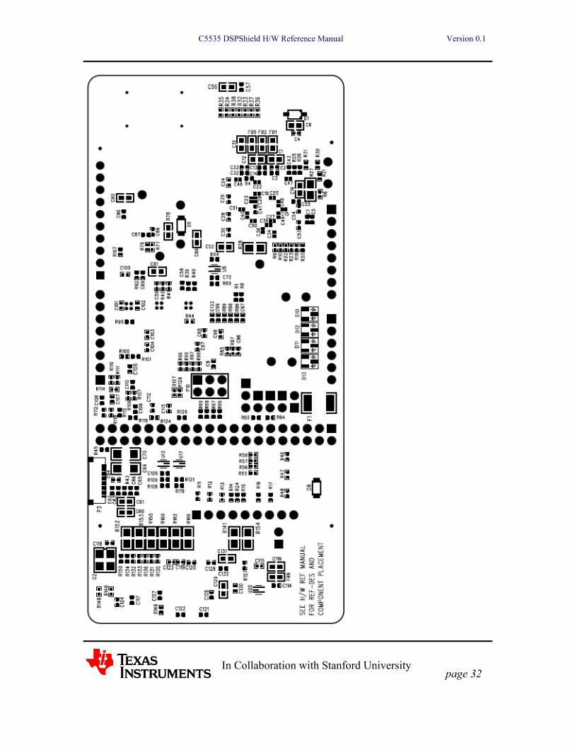
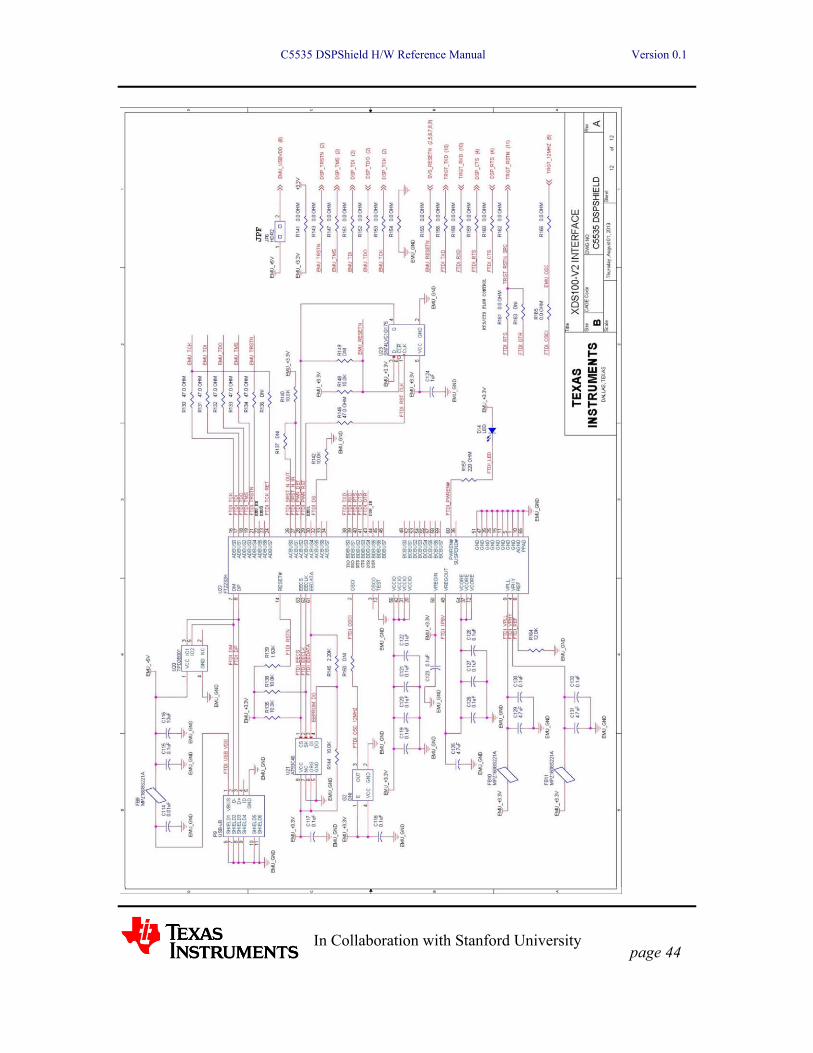
9 Assembly Drawings and Schematics
C5535 DSPShield H/W Reference Manual Version 0.1
In Collaboration with Stanford University
page 32

C5535 DSPShield H/W Reference Manual Version 0.1
In Collaboration with Stanford University
page 33

C5535 DSPShield H/W Reference Manual Version 0.1
In Collaboration with Stanford University
page 34

C5535 DSPShield H/W Reference Manual Version 0.1
In Collaboration with Stanford University
page 35

C5535 DSPShield H/W Reference Manual Version 0.1
In Collaboration with Stanford University
page 36

C5535 DSPShield H/W Reference Manual Version 0.1
In Collaboration with Stanford University
page 37

C5535 DSPShield H/W Reference Manual Version 0.1
In Collaboration with Stanford University
page 38

C5535 DSPShield H/W Reference Manual Version 0.1
In Collaboration with Stanford University
page 39

C5535 DSPShield H/W Reference Manual Version 0.1
In Collaboration with Stanford University
page 40

C5535 DSPShield H/W Reference Manual Version 0.1
In Collaboration with Stanford University
page 41

C5535 DSPShield H/W Reference Manual Version 0.1
In Collaboration with Stanford University
page 42

C5535 DSPShield H/W Reference Manual Version 0.1
In Collaboration with Stanford University
page 43
C5535 DSPShield H/W Reference Manual Version 0.1
In Collaboration with Stanford University
page 44