Embed Size (px)
Citation preview
T. F. Smith Professor.
Member ASME
C. Beckermann Assistant Professor. Assoc. Mem. ASME
Department of Mechanical Engineering, The University of Iowa, Iowa City, Iowa 52242
S. W. Weber Technical Staff Member,
Systems Engineering and Analysis, Collins Defense Communications,
Rockwell International Corporation, Cedar Rapids, Iowa 52498
Combined Conduction, Natural Convection and Radiation Heat Transfer in an Electronic Chassis A numerical study of the combined heat transfer by conduction, natural convection, and radiation in a sealed electronic package is reported. The goal of the study is to investigate the importance of the various heat transfer modes, the effectiveness of different heat transfer paths, and the impact of a number of design changes on the overall thermal performance of a typical electronic package. The package consists of an enclosure containing three printed circuit boards on which are mounted various heat-generating electronic components. Heat transfer processes at both small (i.e., inside a component) and large (i.e., the package) scales as well as all heat transfer modes are included simultaneously in the numerical model. Both one and two-dimensional radiation is considered. Results are presented in terms of streamline and isotherm plots and average temperatures and heat transfer rates. Overall, the numerical data show favorable agreement with available empirical data. One significant conclusion is that natural convection inside the enclosure has only a minor effect on the heat transfer in the present system.
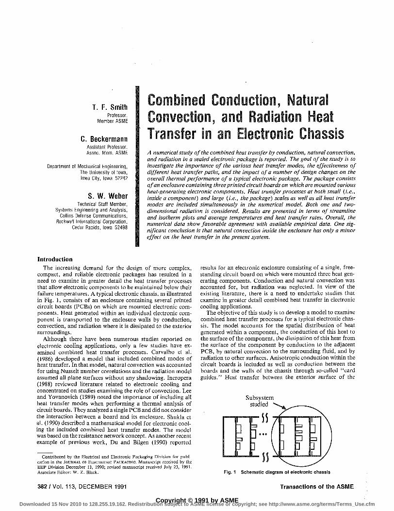
Introduction The increasing demand for the design of more complex,
compact, and reliable electronic packages has resulted in a need to examine in greater detail the heat transfer processes that allow electronic components to be maintained below their failure temperatures. A typical electronic chassis, as illustrated in Fig. 1, consists of an enclosure containing several printed circuit boards (PCBs) on which are mounted electronic components. Heat generated within an individual electronic component is transported to the enclosure walls by conduction, convection, and radiation where it is dissipated to the exterior surroundings.
Although there have been numerous studies reported on electronic cooling applications, only a few studies have examined combined heat transfer processes. Carvalho et al. (1986) developed a model that included combined modes of heat transfer. In that model, natural convection was accounted for using Nusselt number correlations and the radiation model assumed all plane surfaces without any shadowing. Incropera (1988) reviewed literature related to electronic cooling and concentrated on studies examining the role of convection. Lee and Yovanovich (1989) noted the importance of including all heat transfer modes when performing a thermal analysis of circuit boards. They analyzed a single PCB and did not consider the interaction between a board and its enclosure. Shukla et al. (1990) described a mathematical model for electronic cooling the included combined heat transfer modes. The model was based on the resistance network concept. As another recent example of previous work, Du and Bilgen (1990) reported
results for an electronic enclosure consisting of a single, freestanding circuit board on which were mounted three heat generating components. Conduction and natural convection was accounted for, but radiation was neglected. In view of the existing literature, there is a need to undertake studies that examine in greater detail combined heat transfer in electronic cooling applications.
The objective of this study is to develop a model to examine combined heat transfer processes for a typical electronic chassis. The model accounts for the spatial distribution of heat generated within a component, the conduction of this heat to the surface of the component, the dissipation of this heat from the surface of the component by conduction to the adjacent PCB, by natural convection to the surrounding fluid, and by radiation to other surfaces. Anisotropic conduction within the circuit boards is included as well as conduction between the boards and the walls of the chassis through so-called "card guides." Heat transfer between the exterior surface of the
Subsystem studied
Contributed by the Electrical and Electronic Packaging Division for publication in the JOURNAL OF ELECTRONIC PACKAGING. Manuscript received by the EEP Division December 13, 1990; revised manuscript received July 23, 1991. Associate Editor: W. Z. Black.
1 : Z3
] |
Ps7\ 1"' (
1 ]
J 1
r ™
13
L
r : __!
]
Fig. 1 Schematic diagram of electronic chassis
382 / Vol. 113, DECEMBER 1991 Transactions of the ASME
Copyright © 1991 by ASMEDownloaded 15 Nov 2010 to 128.255.19.162. Redistribution subject to ASME license or copyright; see http://www.asme.org/terms/Terms_Use.cfm
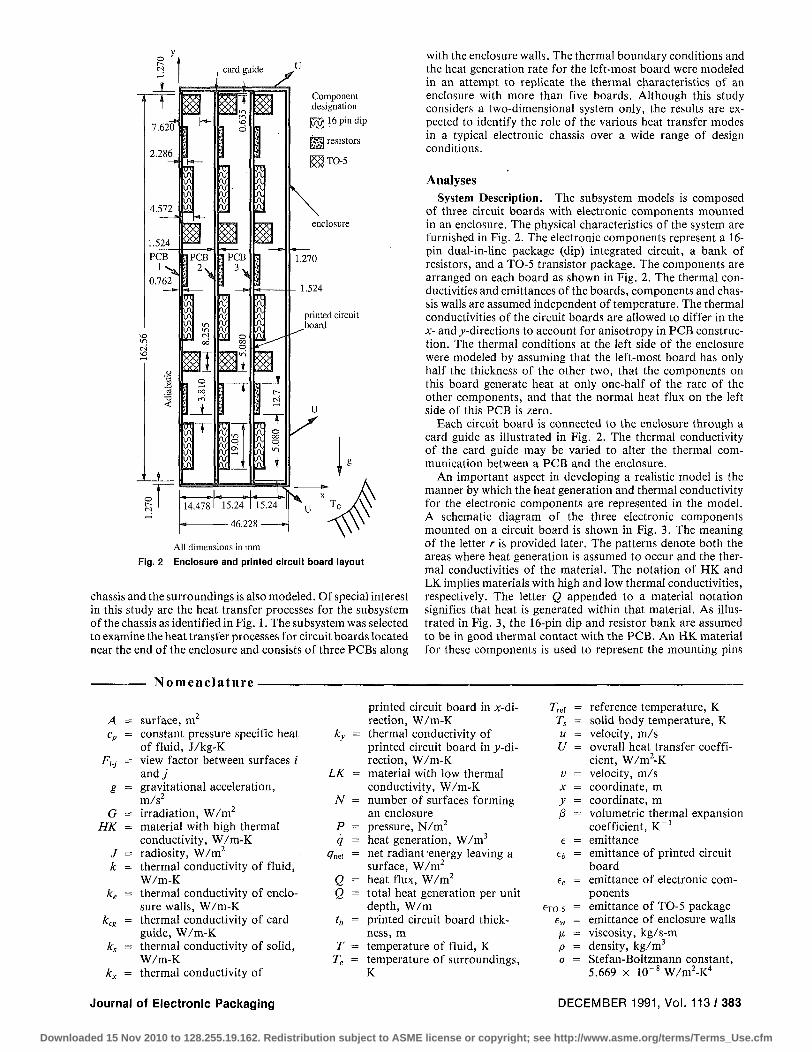
with the enclosure walls. The thermal boundary conditions and the heat generation rate for the left-most board were modeled in an attempt to replicate the thermal characteristics of an enclosure with more than five boards. Although this study considers a two-dimensional system only, the results are expected to identify the role of the various heat transfer modes in a typical electronic chassis over a wide range of design conditions.
Analyses System Description. The subsystem models is composed
of three circuit boards with electronic components mounted in an enclosure. The physical characteristics of the system are furnished in Fig. 2. The electronic components represent a 16-pin dual-in-line package (dip) integrated circuit, a bank of resistors, and a TO-5 transistor package. The components are arranged on each board as shown in Fig. 2. The thermal conductivities and emittances of the boards, components and chassis walls are assumed independent of temperature. The thermal conductivities of the circuit boards are allowed to differ in the x- and jy-directions to account for anisotropy in PCB construction. The thermal conditions at the left side of the enclosure were modeled by assuming that the left-most board has only half the thickness of the other two, that the components on this board generate heat at only one-half of the rate of the other components, and that the normal heat flux on the left side of this PCB is zero.
Each circuit board is connected to the enclosure through a card guide as illustrated in Fig. 2. The thermal conductivity of the card guide may be varied to alter the thermal communication between a PCB and the enclosure.
An important aspect in developing a realistic model is the manner by which the heat generation and thermal conductivity for the electronic components are represented in the model. A schematic diagram of the three electronic components mounted on a circuit board is shown in Fig. 3. The meaning of the letter r is provided later. The patterns denote both the areas where heat generation is assumed to occur and the thermal conductivities of the material. The notation of HK and LK implies materials with high and low thermal conductivities, respectively. The letter Q appended to a material notation signifies that heat is generated within that material. As illustrated in Fig. 3, the 16-pin dip and resistor bank are assumed to be in good thermal contact with the PCB. An HK material for these components is used to represent the mounting pins
Nomenclature
A Cp
Fi-i
8
G HK
J k
K
Kcg
k,
kx
= surface, m2
= constant pressure specific heat of fluid, J/kg-K
= view factor between surfaces i andy
= gravitational acceleration, m/s2
= irradiation, W/m2
= material with high thermal conductivity, W/m-K
= radiosity, W/m2
= thermal conductivity of fluid, W/m-K
= thermal conductivity of enclosure walls, W/m-K
= thermal conductivity of card guide, W/m-K
= thermal conductivity of solid, W/m-K
= thermal conductivity of
kv
LK
N
P q
<7net
Q Q
h
T T 1 e
printed circuit board in x-di-rection, W/m-K
= thermal conductivity of printed circuit board in .y-di-rection, W/m-K
= material with low thermal conductivity, W/m-K
= number of surfaces forming an enclosure
= pressure, N/m2
= heat generation, W/m3
= net radiant energy leaving a surface, W/m2
= heat flux, W/m2
= total heat generation per unit depth, W/m
= printed circuit board thickness, m
= temperature of fluid, K = temperature of surroundings,
K
Tref T 1 s U
u V
X
y &
e
e*
ec
fTO-5
«w
/* P a
= reference temperature, K = solid body temperature, K = velocity, m/s = overall heat transfer coeffi
cient, W/m2-K = velocity, m/s = coordinate, m = coordinate, m = volumetric thermal expansion
coefficient, K~' = emittance = emittance of printed circuit
board = emittance of electronic com
ponents = emittance of TO-5 package = emittance of enclosure walls = viscosity, kg/s-m = density, kg/m3
= Stefan-Boltzmann constant, 5.669 x 1(T8 W/m2-K4
Component designation g g 16 pin dip
All dimensions in mm
Fig. 2 Enclosure and printed circuit board layout
chassis and the surroundings is also modeled. Of special interest in this study are the heat transfer processes for the subsystem of the chassis as identified in Fig. 1. The subsystem was selected to examine the heat transfer processes for circuit boards located near the end of the enclosure and consists of three PCBs along
Journal of Electronic Packaging DECEMBER 1991, Vol. 113 / 383
Downloaded 15 Nov 2010 to 128.255.19.162. Redistribution subject to ASME license or copyright; see http://www.asme.org/terms/Terms_Use.cfm
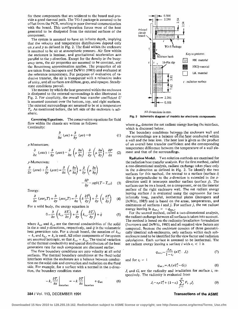
for these components that are soldered to the board and provide a good thermal path. The TO-5 package is assumed to be offset from the PCB, resulting in poor thermal communication with the board. This configuration forces most of the heat generated to be dissipated from the external surfaces of the component.
The system is assumed to have an infinite depth, implying that the velocity and temperature distributions depend only on x and y as defined in Fig. 2. The fluid within the enclosure is assumed to be air at atmospheric pressure. Air flow within the enclosure is laminar, and gravitational acceleration acts parallel to the y-direction. Except for the density in the buoyancy term, the air properties are assumed to be constant, and the Boussinesq approximation applies. The properties of air are taken from Incropera and DeWitt (1985) and evaluated at the reference temperature. For purposes of evaluation of radiative transfer, the air is transparent with a refractive index of unity, and all surfaces are diffuse, gray, and opaque. Steady-state conditions prevail.
The manner by which the heat generated within the enclosure is dissipated to the external surroundings is also illustrated in Fig. 2. For simplicity, the overall heat transfer coefficient U is assumed constant over the bottom, top, and right surfaces. The external surroundings are assumed to be at a temperature Te. As mentioned before, the left side of the enclosure is adi-abatic.
Governing Equations. The conservation equations for fluid flow within the chassis are written as follows: Continuity:
— (pu)+— (pv)=0 ox dy
x-Momentum: d , x ° , , d / du\ d [ du\
^-Momentum:
d , x d , % d ( dv\ d I dv\
- — + Pgl3(T-dy
dP
~ dx
- Tra)
(1)
(2)
(3)
Energy:
— (pucpT)+— (pvcpT)= — dx " dy dx
a n _a_ i dT dy)+dy \ dy
For a solid body, the energy equation is
d / . 3 rA d (. dJ\
dy 0
dx\ks'x~dx)+dy \ks'y + q
(4)
(5)
where kSiX and kSiy are the thermal conductivities of the solid in thex- and ^-directions, respectively, and q is the volumetric heat generation rate. For a circuit board, the notation of kSiX
= kx and ks<y = ky is used. All other components of the system are assumed isotropic, so that kStX = kSty. The spatial variation of the thermal conductivity and spatial distribution of the heat generation rate for each component are discussed earlier.
The flow boundary conditions are zero velocity at all solid surfaces. The thermal boundary conditions at the fluid/solid interfaces within the enclosure are a balance between conduction on the solid side and convection and radiation on the fluid side. For example, for a surface with a normal in the x-direc-tion, the boundary condition states
k ^ ks dx , dT
= ~kTx + <7net (6)
Printed circuit board
\
0.508 2.286
3 TO-5 Package
Resistor bank
16-Pin dip
Key to patterns:
I 1 HK materia!
| j j j HKQ material
LK material
r - radiation surface
2.286
• 0.508
All dimensions in mm.
Fig. 3 Schematic diagram of models for electronic components
where qnet denotes the net radiant energy leaving the interface, which is discussed below.
The boundary conditions between^, the enclosure wall and the surroundings are a balance oft the; heat conducted within a wall and the heat loss. The heat loss is given as the product of an overall heat transfer coefficient and the corresponding temperature difference between the temperature of a wall element and that of the surroundings.
Radiation Model. Two solution methods are examined for the radiation heat transfer analysis. For the first method, called a one-dimensional analysis, radiant exchange takes place only in the x-direction as defined in Fig. 2. To identify the two surfaces for this method, the normal to a surface (surface i) that is perpendicular to the x-direction is extended in the x-direction until it intercepts another surface (surface J). The surfaces can be on a board, on a component, or on the interior surface of the right enclosure wall. The net radiant energy leaving surface / is evaluated using the expression for two infinitely long, parallel, isothermal plates (Incropera and DeWitt, 1985) and is based on the areas, temperatures, and emittances of surfaces / and j . For surface j , the net radiant energy leaving is qmtJ = - qaa<i.
For the second method, called a two-dimensional analysis, the radiant exchange between all surfaces is taken into account. The method is based on the radiosity/irradiation formulation (Incropera and DeWitt, 1985) and all required view factors are computed. Because the enclosure consists of three geometrically identical sub-enclosures, only surfaces within each sub-enclosure need to be identified for the view factor and radiation calculations. Each surface is assumed to be isothermal. The net radiant energy leaving a surface /' with e,- < 1 is
tfnet,; = 7-LL(tf7f--A) 1-e, (7)
and for e, = 1
qKt.i=M<jTl-G,) (8)
J, and G/ are the radiosity and irradiation for surface /, respectively. The radiosity is evaluated from
/, = 6 ; t T 7 ? + ( l - e , ) 2 ^ w 4 y=i
(9)
384 / Vol. 113, DECEMBER 1991 Transactions of the AS ME
Downloaded 15 Nov 2010 to 128.255.19.162. Redistribution subject to ASME license or copyright; see http://www.asme.org/terms/Terms_Use.cfm
Table 1 Conditions for Case 1 (base case)
Symbol Description Value Units
Table 2 Conditions and results for average and maximum temperature rises for other cases*
g gravitational acceleration 9.81 m/s HK high-thermal-conductivity material 100 W/m-K LK low-thermal-conductivity material 0.1 W/m-K ke thermal conductivity of enclosure walls 138 W/m-K kcg thermal conductivity of card guide 4.69 W/m-K kx thermal conductivity of PCB in ^--direction 3.45 W/m-K ky thermal conductivity of PCB in j>-direction 18.5 W/m-K
Q total heat generation per unit depth 118 W/m each component: 5.24 W/m components on left PCB: 2.63 W/m
tb thickness of PCBs (left: tb/2) 1.52 mm Trcr reference temperature for air properties 86.9 °C Te temperature of surroundings 24.9 °C U overall heat transfer coefficient 10 W/m2-K eb emittance of PCB 0.8 ec emittance of electronic components 0.8 e„ emittance of enclosure interior surfaces 0.5
where Fj.j is the view factor between surfaces / and j and N is the number of surfaces forming the radiation sub-enclosure. The irradiation is given by
G,= J]F,jJj (10) y'=i
Equation (9) is solved for the radiosities using an iterative procedure. Because all surfaces are planar, F^ = 0. The remaining view factors are determined using the Hottel cross-string method (Siegel and Howell, 1981), which is applicable for infinite strips. Any blockage of the view between surfaces i and j is accounted for. The reciprocity relation is used to reduce the number of view factors. The enclosure relation serves to verify the accuracy of the computations for the view factors and to obtain the view factors for only two surfaces whose view may be blocked by at most three others surfaces.
Numerical Procedure Numerical solutions of the governing conservation equations
are obtained using the control-volume formulation and the SIMPLER algorithm detailed in Patankar (1980). In a similar manner as House et al. (1990), one set of conservation equations is solved over the entire domain. By setting the viscosity to infinity in the region occupied by the solid body, the velocities approach zero in this region. At the same locations, the diffusion coefficient (thermal conductivity) in the energy equation is changed from that for the fluid to that for the solid. By combining the energy equations in this manner and accounting for a surface radiation term (Beckermann and Smith, 1990), the matching conditions at the fluid/solid interfaces such as stated by Eq. (6) are satisfied automatically. The harmonic mean formulation adopted for the interface diffusion coefficients between two control volumes yields physically realistic results for abrupt changes in these coefficients without requiring an excessively fine grid in the neighborhood of the fluid/solid interfaces. Convergence of the numerical solution was checked by performing overall mass and energy balances.
A nonuniform grid spacing is used to resolve velocity and temperature fields. The grid spacing in the x-direction is 0.762 mm for the left-most PCB, 1.524 mm for the other two boards, and 1.270 mm for the right enclosure wall. Starting from the right surface of a circuit board, the grid is 2.286, 0.508, 1.778, and 1.524 mm, where the latter spacing continues until the next board or enclosure wall is reached. Except for the spacing near the top of a TO-5 component and at the very top of the circuit boards, where the grid spacing is 0.635 mm, the grid spacing in the .y-direction is 1.270 mm. There are 33 nodes in the x-direction and 136 nodes in the ^-direction.
Case Description
(a) Importance of heat transfer modes.
1 Base case 2 No convection 3 No radiation 4 No radiation and no convection 5 kcg = 0.01 W/m-K 6 kcg = 0.01 W/m-K and no convection 7 kcg = 0.01 W/m-K and no radiation
(b) Validity of 1-D radiation model.
8 1-D radiation model 9 Case 5, but 1-D radiation model
(c) Effect of temperature level.
10 Q = 59.06 W/m 11 U = 7 W/m2-K 12 ( 7 = 7 W/m2-K, no radiation
(d) Effect of component thermal conductivities,
13 HK = 10 W/m-K 14 LK = 1.0 W/m-K 15 HK = 10 W/m-K, LK = 1.0 W/m-K
(e) Effect of TO-5 emittance.
16 eTO-5 = 0.2 17 eT0.5 = 0.5 18 eTo-5 = 1.0
(f) Effect of other design changes.
19 e„ = 0.8 20 k, = 4.86 W/m-K, kx = 3.44 W/m-K,
kcs = 16.4 W/m-K, 21 Case 20, but kc. = 2.73 W/m-K 22 ky = 34.5 W/m-K, kx = 3.47 W/m-K,
kcg = 12.3 W/m-K, tb = 2.03 mm 23 ky = 56.2 W/m-K, kx = 3.03 W/m-K,
kcg = 1 1 . 6 W/m-K, t„ = 2.16 mm 24 Case 22, but kcg = 2.06 W/m-K
ATb, °C
63.1 63.1 66.0 66.2
100.1 101.7 142.5
63.5 108.3
31.8 82.2 85.5
64.6 63.3 64.9
63.4 63.2 63.0
62.2 73.6
75.8 56.5
54.8
60.2
Armax, °c
74.4 74.2 80.5 80.3
112.0 112.9 165.6
76.6 122.1
37.9 93.1
101.0
77.0 70.5 73.5
76.9 75.5 73.9
73.4 89.5
91.7 66.4
64.0
70.0
'Conditions for Case 1 apply except where noted.
For the one-dimensional radiation model, the net radiant energy is found for every control volume with a vertical surface. The grid pattern for the two-dimensional radiation analysis can be identified by reference to Fig. 3, where representative radiation surfaces for the analysis are identified by the letter r. A total of 72 surfaces forms the radiation sub-enclosure. Because the grid patterns for the control volume analysis and the two-dimensional radiation model do not coincide, the temperatures of the surfaces in Fig. 3 are obtained by averaging the appropriate nodal temperatures. The radiant heat flux computed from the two-dimensional analysis is distributed uniformly over each surface and is incorporated with the finite control volume analysis.
The accuracy of the numerical solution was verified by performing grid studies and comparisons with benchmark solutions for certain limiting cases (House et al., 1990). As shown in the following, the convection intensity in virtually all of the present simulations is very low, eliminating the need to resolve large velocity gradients.
Numerical simulations were performed on an ENCORE computer system. A typical case involving all heat transfer modes required approximately 2000 s of central processing unit time to achieve convergence; cases considering only conduction required about 100 s.
Description of Test Cases The effects of various design parameters and heat transfer
modes on the flow patterns and temperature distributions are investigated in a number of test cases. The test cases investigate sensitivity to
(1) thermal conductivities of circuit boards and electronic components,
Journal of Electronic Packaging DECEMBER 1991, Vol. 113 / 385
Downloaded 15 Nov 2010 to 128.255.19.162. Redistribution subject to ASME license or copyright; see http://www.asme.org/terms/Terms_Use.cfm
i iff l i J if ....'. \\-—JL
i i * * i •
J juu * •
1 | | : : |
I I (I l i
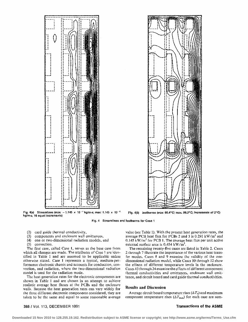
Fig. 4(a) Streamlines (min: -1.145 x 10 4 kg/m-s; max: 1.145 x 10 kg/m-s; 16 equal Increments)
Fig. 4(b) Isotherms (min: 66.4°C; max: 99.2°C; increments of 2°C)
Fig. 4 Streamlines and isotherms for Case 1
(2) card guide thermal conductivity, (3) components and enclosure wall emittances, (4) one or two-dimensional radiation models, and (5) convection. The first case, called Case 1, serves as the base case from
which all changes are made. The attributes of Case 1 are identified in Table 1 and are assumed to be applicable unless otherwise stated. Case 1 represents a typical, medium-performance electronic chassis and accounts for conduction, convection, and radiation, where the two-dimensional radiation model is used for the radiation mode.
The heat generation rates for the electronic components are shown in Table 1 and are chosen in an attempt to achieve realistic average heat fluxes at the PCBs and the enclosure walls. Because the heat generation rates can vary widely for the three different electronic components considered, they are taken to be the same and equal to some reasonable average
value (see Table 1). With the present heat generation rates, the average PCB heat flux for PCBs 2 and 3 is 0.291 kW/m2 and 0.145 kW/m2 for PCB 1. The average heat flux per unit active external surface area is 0.454 kW/m2.
The remaining twenty-five cases are listed in Table 2. Cases 2 through 7 illustrate the importance of the various heat transfer modes. Cases 8 and 9 examine the validity of the one-dimensional radiation model, while Cases 10 through 12 show the effects of different temperature levels in the enclosure. Cases 13 through 24 examine the effects of different component thermal conductivities and emittances, enclosure wall emit-tance, and circuit board and card guide thermal conductivities.
Results and Discussion Average circuit board temperature rises (A Tb) and maximum
component temperature rises (ATm!a) for each case are sum-
386 / Vol. 113, DECEMBER 1991 Transactions of the ASME
Downloaded 15 Nov 2010 to 128.255.19.162. Redistribution subject to ASME license or copyright; see http://www.asme.org/terms/Terms_Use.cfm
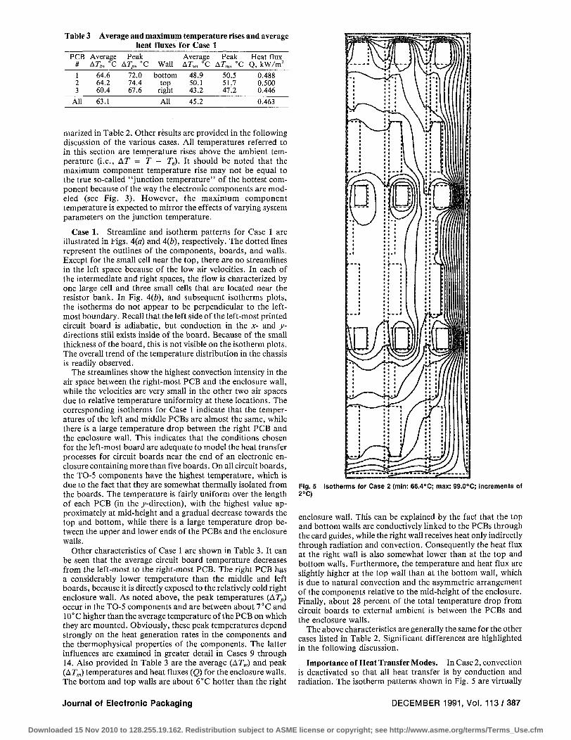
Table 3 Average and maximum temperature rises and average heat fluxes for Case 1
PCB Average # AT„, °C
1 64.6 2 64.2 3 60.4
All 63.1
Peak AT,, °C
72.0 74.4 67.6
Wall
bottom top
right
All
Average
48.9 50.1 43.2
45.2
Peak Ar,„, °c
50.5 51.7
.47.2
Heat flux Q, kW/m2
0.488 0.500 0.446
0.463
marized in Table 2. Other results are provided in the following discussion of the various cases. All temperatures referred to in this section are temperature rises above the ambient temperature (i.e., AT = T — Te). It should be noted that the maximum component temperature rise may not be equal to the true so-called "junction temperature" of the hottest component because of the way the electronic components are modeled (see Fig. 3). However, the maximum component temperature is expected to mirror the effects of varying system parameters on the junction temperature.
Case 1. Streamline and isotherm patterns for Case 1 are illustrated in Figs. 4(a) and 4(b), respectively. The dotted lines represent the outlines of the components, boards, and walls. Except for the small cell near the top, there are no streamlines in the left space because of the low air velocities. In each of the intermediate and right spaces, the flow is characterized by one large cell and three small cells that are located near the resistor bank. In Fig. 4(b), and subsequent isotherms plots, the isotherms do not appear to be perpendicular to the leftmost boundary. Recall that the left side of the left-most printed circuit board is adiabatic, but conduction in the x- and y-directions still exists inside of the board. Because of the small thickness of the board, this is not visible on the isotherm plots. The overall trend of the temperature distribution in the chassis is readily observed.
The streamlines show the highest convection intensity in the air space between the right-most PCB and the enclosure wall, while the velocities are very small in the other two air spaces due to relative temperature uniformity at these locations. The corresponding isotherms for Case 1 indicate that the temperatures of the left and middle PCBs are almost the same, while there is a large temperature drop between the right PCB and the enclosure wall. This indicates that the conditions chosen for the left-most board are adequate to model the heat transfer processes for circuit boards near the end of an electronic enclosure containing more than five boards. On all circuit boards, the TO-5 components have the highest temperature, which is due to the fact that they are somewhat thermally isolated from the boards. The temperature is fairly uniform over the length of each PCB (in the .y-direction), with the highest value approximately at mid-height and a gradual decrease towards the top and bottom, while there is a large temperature drop between the upper and lower ends of the PCBs and the enclosure walls.
Other characteristics of Case 1 are shown in Table 3. It can be seen that the average circuit board temperature decreases from the left-most to the right-most PCB. The right PCB has a considerably lower temperature than the middle and left boards, because it is directly exposed to the relatively cold right enclosure wall. As noted above, the peak temperatures (ATP) occur in the TO-5 components and are between about 7°C and 10°C higher than the average temperature of the PCB on which they are mounted. Obviously, these peak temperatures depend strongly on the heat generation rates in the components and the thermophysical properties of the components. The latter influences are examined in greater detail in Cases 9 through 14. Also provided in Table 3 are the average (ATW) and peak (ATm) temperatures and heat fluxes (Q) for the enclosure walls. The bottom and top walls are about 6°C hotter than the right
Fig. 5 Isotherms for Case 2 (min: 66.4°C; max: 99.0°C; increments of 2°C)
enclosure wall. This can be explained by the fact that the top and bottom walls are conductively linked to the PCBs through the card guides, while the right wall receives heat only indirectly through radiation and convection. Consequently the heat flux at the right wall is also somewhat lower than at the top and bottom walls. Furthermore, the temperature and heat flux are slightly higher at the top wall than at the bottom wall, which is due to natural convection and the asymmetric arrangement of the components relative to the mid-height of the enclosure. Finally, about 28 percent of the total temperature drop from circuit boards to external ambient is between the PCBs and the enclosure walls.
The above characteristics are generally the same for the other cases listed in Table 2. Significant differences are highlighted in the following discussion.
Importance of Heat Transfer Modes. In Case 2, convection is deactivated so that all heat transfer is by conduction and radiation. The isotherm patterns shown in Fig. 5 are virtually
Journal of Electronic Packaging DECEMBER 1991, Vol. 113 / 387
Downloaded 15 Nov 2010 to 128.255.19.162. Redistribution subject to ASME license or copyright; see http://www.asme.org/terms/Terms_Use.cfm
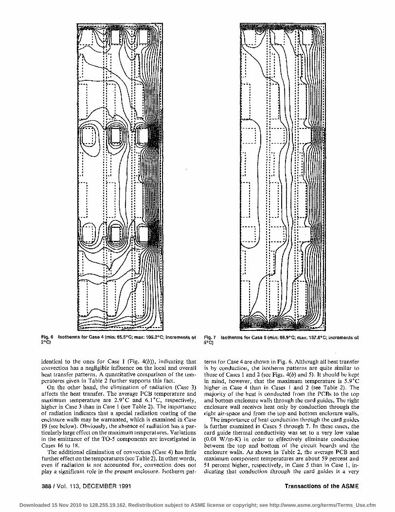
Fig. 6 Isotherms for Case 4 (min: 65.5°C; max: 105.2°C; increments of 2°C)
identical to the ones for Case 1 (Fig. 4(b)), indicating that convection has a negligible influence on the local and overall heat transfer patterns. A quantitative comparison of the temperatures given in Table 2 further supports this fact.
On the other hand, the elimination of radiation (Case 3) affects the heat transfer. The average PCB temperature and maximum temperature are 2.9°C and 6.1°C, respectively, higher in Case 3 than in Case 1 (see Table 2). The importance of radiation indicates that a special radiation coating of the enclosure walls may be warranted, which is examined in Case 19 (see below). Obviously, the absence of radiation has a particularly large effect on the maximum temperatures. Variations in the emittance of the TO-5 components are investigated in Cases 16 to 18.
The additional elimination of convection (Case 4) has little further effect on the temperatures (see Table 2). In other words, even if radiation is not accounted for, convection does not play a significant role in the present enclosure. Isotherm pat-
388 / Vol. 113, DECEMBER 1991
Fig. 7 Isotherms for Case 6 (min: 68.9°C; max: 137.8°G; increments of 5°C)
terns for Case 4 are shown in Fig. 6. Although all heat transfer is by conduction, the isotherm patterns are quite similar to those of Cases 1 and 2 (see Figs. 4(b) and 5). It should be kept in mind, however, that the maximum temperature is 5.9°C higher in Case 4 than in Cases 1 and 2 (see Table 2). The majority of the heat is conducted from the PCBs to the top and bottom enclosure walls through the card guides. The right enclosure wall receives heat only by conduction through the right air-space and from the top and bottom enclosure walls.
The importance of heat conduction through the card guides is further examined in Cases 5 through 7. In these cases, the card guide thermal conductivity was set to a very low value (0.01 W/m-K) in order to effectively eliminate conduction between the top and bottom of the circuit boards and the enclosure walls. As shown in Table 2, the average PCB and maximum component temperatures are about 59 percent and 51 percent higher, respectively, in Case 5 than in Case 1, indicating that conduction through the card guides is a very
Transactions of the ASME
Downloaded 15 Nov 2010 to 128.255.19.162. Redistribution subject to ASME license or copyright; see http://www.asme.org/terms/Terms_Use.cfm
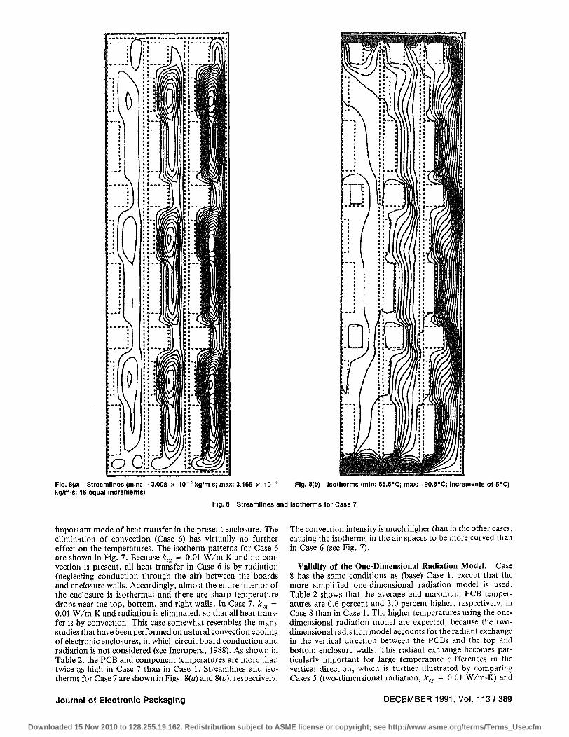
Fig. 8(a) Streamlines (min: -3.008 x 10 " kg/m-s; max: 3.165 x 10 kg/m-s; 16 equal increments)
Fig. 8(b) Isotherms (min: 66.6°C; max: 190.5°C; increments of 5°C)
Fig. 8 Streamlines and isotherms for Case 7
important mode of heat transfer in the present enclosure. The elimination of convection (Case 6) has virtually no further effect on the temperatures. The isotherm patterns for Case 6 are shown in Fig. 7. Because kcg = 0.01 W/m-K and no convection is present, all heat transfer in Case 6 is by radiation (neglecting conduction through the air) between the boards and enclosure walls. Accordingly, almost the entire interior of the enclosure is isothermal and there are sharp temperature drops near the top, bottom, and right walls. In Case 1, kcg = 0.01 W/m-K and radiation is eliminated, so that all heat transfer is by convection. This case somewhat resembles the many studies that have been performed on natural convection cooling of electronic enclosures, in which circuit board conduction and radiation is not considered (see Incropera, 1988). As shown in Table 2, the PCB and component temperatures are more than twice as high in Case 7 than in Case 1. Streamlines and isotherms for Case 7 are shown in Figs. 8(a) and 8(6), respectively.
The convection intensity is much higher than in the other cases, causing the isotherms in the air spaces to be more curved than in Case 6 (see Fig. 7).
Validity of the One-Dimensional Radiation Model. Case 8 has the same conditions as (base) Case 1, except that the more simplified one-dimensional radiation model is used. Table 2 shows that the average and maximum PCB temperatures are 0.6 percent and 3.0 percent higher, respectively, in Case 8 than in Case 1. The higher temperatures using the one-dimensional radiation model are expected, because the two-dimensional radiation model accounts for the radiant exchange in the vertical direction between the PCBs and the top and bottom enclosure walls. This radiant exchange becomes particularly important for large temperature differences in the vertical direction, which is further illustrated by comparing Cases 5 (two-dimensional radiation, kcg = 0.01 W/m-K) and
Journal of Electronic Packaging DECEMBER 1991, Vol. 113 / 389
Downloaded 15 Nov 2010 to 128.255.19.162. Redistribution subject to ASME license or copyright; see http://www.asme.org/terms/Terms_Use.cfm
60
50
40
30
20
10
0
• e
-
•
.
•
Historial data
Numerical data
Thermal designs;
Minimal
o /
/ ° o / o y
7 ° /
/ s °
' o o
° %
0
o /
/ Case lv
/ • / O , / "
/ Typical / Q
o > o /
o
y Highly ,-, « augmented
.Case 10
o
o
-
-
*s
Fig
0.1 0.2 0.3 0.4 2
Enclosure heat flux level, kW/m 9 Comparison with historical data
9 (one-dimensional radiation, kcg = 0.01 W/m-K). Due to the low card guide thermal conductivity, temperature differences between the PCBs and enclosure walls are much larger (see the previous section). Consequently, the one-dimensional radiation model (Case 9) causes errors in circuit board temperatures of more than 9 percent relative to Case 5 (see Table 2). These findings indicate the importance of accurately accounting for radiation exchange in the electronic enclosure.
Effect of Temperature Level. The overall temperature level in the enclosure can be changed by choosing different heat generation rates in the components (Case 10) or by varying the overall heat transfer coefficient between the enclosure and the surroundings (Cases 11 and 12). In Case 10, the power level is reduced by 50 percent relative to Case 1; however, the PCB temperatures are only about 49.6 percent lower. This small non-linearity can be attributed to radiative heat transfer. Average PCB temperature rises versus the power level per unit area of active external surface area for Cases 1 and 10 are plotted in Fig. 9 as filled symbols and compared to experimental measurements (open symbols) on a large variety of electronic packages produced by Rockwell International Corporation (Weber, 1990). For reference, three regions corresponding to minimal, typical, and highly augmented thermal designs of electronic packages are shown in Fig. 9. It can be seen that the present simulations of a "typical" package fall well within the range of the "historical" data (see also Bar-Cohen and Kraus, 1981). The present results for the board temperatures are slightly below the average of the "typical" designs. This may be attributed to the subsystem studied (see Fig. 1) being at the end of the electronic chassis where the thermal communication to the surroundings is greater than that for circuit boards in the center portion of the chassis. More detailed comparisons are not possible at the present time, because none of the tested packages had the same design as the one simulated here.
In Cases 11 and 12, the overall heat transfer coefficient is decreased from 10 (Case 1) to 7 W/m2-K, causing an increase in the average enclosure wall temperature of 19.5°C. Due to this higher temperature level, radiation can be expected to play a more important role. The average board temperature in Case 11 is 19.1°C higher than in Case 1; the non-linearity due to radiation is somewhat larger at higher temperatures. In Case 12, radiation was eliminated so that this case should be compared to Case 3. Because conduction and convection do not depend on the temperature level, one gets, as expected, a 19.5 °C increase in the PCB temperature for the 19.5 °C increase in the enclosure wall temperature.
0 70
<i 60
1 50 g I 40
1 30 O x>
& 20
< 10
0
75.8
o o o o m. a.
73.6
11
63.1
n
60.2
a-« t - X) o o o o o, on
56.5
11
54.8
1$ 21 20 24 22 23
Fig. 10 Average board temperature rises for various circuit board and card guide thermal resistance combinations
Effect of Component Thermal Conductivities. The present simulations are based, in part, on an estimation of the thermal conductivities of the electronic components. The effects of the chosen values for low (LK) and high (HK) component thermal conductivities are examined in Cases 13 through 15, where the two conductivities are independently varied by one order of magnitude from Case 1. As seen in Table 2, decreasing the value of HK by a factor of ten (Case 13) causes increases of 2.4 percent and 3.5 percent in the average and maximum PCB temperatures, respectively, over Case 1. As expected, the effect on the maximum temperature (of the components) is particularly strong. On the other hand, increasing LK by a factor of ten (Case 14), results in a decrease in the maximum temperature of 5.2 percent, whereas the average PCB temperature increases by 0.3 percent. This can be explained by realizing that the LK material is intended to thermally isolate the TO-5 component from the PCB. Hence, if LK is increased, more of the heat generated in the TO-5 flows into the circuit board, causing a decrease in the TO-5 temperature and an increase, albeit small, in the board temperature. The simultaneous reduction of HK and increase of LK by factors of ten (Case 15) offsets the above effects on the maximum temperature (0.9 percent increase), while the average PCB temperature is about the same as in Case 13. Overall, it can be seen that relatively large changes in the component thermal conductivities have an effect of less than 2.5 percent on average board temperatures, indicating that the estimates of HK and LK are not too crucial in assessing the overall performance of the electronic enclosure; however, the effect can be larger on maximum component temperatures.
Effect of TO-5 Emittance. Because the maximum temperatures are exhibited in the TO-5 packages, it is of interest to examine whether a change in the emittance of the TO-5 packages is an effective means of reducing their temperatures. In Cases 16 through 18, the TO-5 emittance is changed from 0.2 to 1.0, which could be accomplished by using special radiation coatings. The maximum temperatures displayed in Table 2 for these cases are the temperatures of the hottest TO-5 component in the enclosure. In general, the TO-5 operates at a lower temperature when the emittance is high. The maximum temperature increases by 3.0°C for a decrease in the emittance from 1.0 to 0.2. Relative to Case 1 with a TO-5 emittance of 0.8, the temperature decreases by only 0.5°C (0.7 percent) for an emittance of 1.0. The largest decrease occurs for lower emittances, where a 1.4°C (1.9 percent) decrease in the maximum temperature is observed when the emittance is increased from 0.2 to 0.5. These findings indicate that the effect of the TO-5 emittance is minimized as long as the emittance is above 0.5.
390 / Vol. 113, DECEMBER 1991 Transactions of the ASME
Downloaded 15 Nov 2010 to 128.255.19.162. Redistribution subject to ASME license or copyright; see http://www.asme.org/terms/Terms_Use.cfm
Effect of Other Design Changes. The following test cases examine the effects oftypical design options on the temperature rises in the enclosure (see Table 2).
A comparison of Cases 1 {ew = 0.5) and 19 (tw = 0.8) illustrates that a higher enclosure wall emittance has a relatively minor effect on the temperatures for the conditions of these cases (about a 1.4 percent decrease from Case 1). However, additional calculations (Beckermann and Smith, 1990) show an 8 percent decrease in the maximum temperature by changing ew from 0.5 to 0.8, if the card guide thermal conductivity is set to a very low value (see'Cases 5 to 7). This further underscores the importance of radiation if conduction through the card guides is eliminated and the temperature of the circuit board is higher.
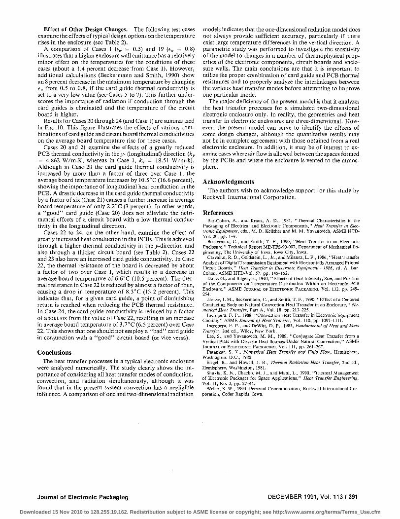
Results for Cases 20 through 24 (and Case 1) are summarized in Fig. 10. This figure illustrates the effects of various combinations of card guide and circuit board thermal conductivities on the average board temperature rise for these cases.
Cases 20 and 21 examine the effects of a greatly reduced PCB thermal conductivity in the/- (longitudinal) direction (ky = 4.862 W/m-K, whereas in Case 1, ky = 18.51 W/m-k). Although in Case 20 the card guide thermal conductivity is increased by more than a factor of three over Case 1, the average board temperature increases by 10.5°C (16.6 percent), showing the importance of longitudinal heat conduction in the PCB. A drastic decrease in the card guide thermal conductivity by a factor of six (Case 21) causes a further increase in average board temperature of only 2.2°C (3 percent). In other words, a "good" card guide (Case 20) does not alleviate the detrimental effects of a circuit board with a low thermal conductivity in the longitudinal direction.
Cases 22 to 24, on the other hand, examine the effect of greatly increased heat conduction in the PCBs. This is achieved through a higher thermal conductivity in the /-direction and also through a thicker circuit board (see Table 2). Cases 22 and 23 also have an increased card guide conductivity. In Case 22, the thermal resistance of the board is decreased by about a factor of two over Case 1, which results in a decrease in average board temperature of 6.6°C (10.5 percent). The thermal resistance in Case 22 is reduced by almost a factor of four, causing a drop in temperature of 8.3°C (13.2 percent). This indicates that, for a given card guide, a point of diminishing return is reached when reducing the PCB thermal resistance. In Case 24, the card guide conductivity is reduced by a factor of about six from the value of Case 22, resulting in an increase in average board temperature of 3.7°C (6.5 percent) over Case 22. This shows that one should not employ a "bad" card guide in conjunction with a "good" circuit board (or vice versa).
Conclusions The heat transfer processes in a typical electronic enclosure
were analyzed numerically. The study clearly shows the importance of considering all heat transfer modes of conduction, convection, and radiation simultaneously, although it was found that in the present system convection has a negligible influence. A comparison of one and two-dimensional radiation
models indicates that the one-dimensional radiation model does not always provide sufficient accuracy, particularly if there exist large temperature differences in the vertical direction. A parametric study was performed to investigate the sensitivity of the model to changes in a number of thermophysical properties of the electronic components, circuit boards and enclosure walls. The main conclusions are that it is important to utilize the proper combination of card guide and PCB thermal resistances and to properly analyze the interlinkages between the various heat' transfer modes before attempting to improve one particular mode.
The major deficiency of the present model is that it analyzes the heat transfer processes for a simulated two-dimensional electronic enclosure only. In reality, the geometries and heat transfer in electronic enclosures are three-dimensional. However, the present model can serve to identify the effects of some design changes, although the quantitative results may not be in complete agreement with those obtained from a real electronic enclosure. In addition, it may be of interest to examine cases where air flow is allowed between the spaces formed by the PCBs and where the enclosure is vented to the atmosphere.
Acknowledgments The authors wish to acknowledge support for this study by
Rockwell International Corporation.
References Bar-Cohen, A., and Kraus, A. D., 1981, "Thermal Characteristics in the
Packaging of Electrical and Electronic Components," Heat Transfer in Electronic Equipment, eds., M. D. Kelleher and M. M. Yovanovich, ASME HTD-Vol. 20, pp. 1-9.
Beckerman, C , and Smith, T. F., 1990, "Heat Transfer in an Electronic Enclosure," Technical Report ME-TFS-90-007, Department of Mechanical Engineering, The University of Iowa, Iowa City, Iowa.
Carvalho, R. D., Goldstein, L., Jr., andMilanez, L. F., 1986, "Heat Transfer Analysis of Digital Transmission Equipment with Horizontally Arranged Printed Circuit Boards," Heat Transfer in Electronic Equipment—1986, ed. A. Bar-Cohen, ASME HTD-Vol. 57, pp. 145-152.
Du, Z-G., and Bilgen, E., 1990, "Effects of Heat Intensity, Size, and Position of the Components on Temperature Distribution Within an Electronic PCB Enclosure," ASME JOURNAL OF ELECTRONIC PACKAGING, Vol. 112, pp. 249-
254. House, J. M., Beckermann, C , and Smith, T. F., 1990, "Effect of a Centered
Conducting Body on Natural Convection Heat Transfer in an Enclosure," Numerical Heat Transfer, Part A, Vol. 18, pp. 213-225.
Incropera, F. P., 1988, "Convection Heat Transfer in Electronic Equipment Cooling," ASME Journal of Heat Transfer, Vol. 110, pp. 1097-1111.
Incropera, F. P., and DeWitt, D. P., 1985, Fundamental of Heat and Mass Transfer, 2nd ed., Wiley, New York.
Lee, S., and Yovanovich, M. M., 1989, "Conjugate Heat Transfer from a Vertical Plate with Discrete Heat Sources Under Natural Convection," ASME JOURNAL OF ELECTRONIC PACKAGING, Vol. I l l , pp. 261-267.
Patankar, S. V., Numerical Heat Transfer and Fluid Flow, Hemisphere, Washington, D.C., 1980.
Siegel, R., and Howell, J. R., Thermal Radiation Heat Transfer, 2nd ed., Hemisphere, Washington, 1981.
Shukla, K. N., Chacko, M. J., and Mani, L., 1990, "Thermal Management of Electronic Packages for Space Applications," Heat Transfer Engineering, Vol. 11, No. 3, pp. 27-44.
Weber, S. W., 1990, Personal Communication, Rockwell International Corporation, Cedar Rapids, Iowa.
Journal of Electronic Packaging DECEMBER 1991, Vol. 113 / 391
Downloaded 15 Nov 2010 to 128.255.19.162. Redistribution subject to ASME license or copyright; see http://www.asme.org/terms/Terms_Use.cfm