Embed Size (px)
Citation preview
arX
iv:p
hysi
cs/0
4090
48 v
1 9
Sep
200
4
The detection of single electrons by means of
a Micromegas-covered MediPix2 pixel CMOS
readout circuit
M. Campbell a, M. Chefdeville b, P. Colas b, A.P. Colijn c,
A. Fornaini c,d, Y. Giomataris b, H. van der Graaf c,E.H.M Heijne a, P. Kluit c, X. Llopart a, J. Schmitz d,
J. Timmermans c, J.L. Visschers c
aCERN/MediPix Consortium, Geneva, SwitzerlandbDAPNIA, CEA Saclay, 91191 Gif sur Yvette Cedex, France
cNIKHEF, Amsterdam, The NetherlandsdUniv. of Twente/MESA, The Netherlands
Corresponding author: Jan Timmermans, NIKHEF, [email protected]
Abstract
A small drift chamber was read out by means of a MediPix2 readout chip asdirect anode. A Micromegas foil was placed 50 µm above the chip, and electronmultiplication occurred in the gap. With a He/Isobutane 80/20 mixture, gas multi-plication factors up to tens of thousands were achieved, resulting in an efficiency fordetecting single electrons of better than 90% . We recorded many frames containing2D images with tracks from cosmic muons. Along these tracks, electron clusterswere observed, as well as δ-rays.
Keywords : Micromegas, MediPix2, TPC, single electron, pixel, pixel segmentedanode
1 Introduction
Recently [1] we have demonstrated the possibility to read out a drift chamberby means of a direct, pixel segmented active anode. Images of the interactionof 55Fe quanta with the gas were obtained (see Figure 1) with a rather low gasamplification factor, since these quanta create some 220 primary electrons ina small volume of argon gas. The aim of the research presented in this letteris to prove the feasibility of the detection of single (drifting) electrons, basedon the same pixel sensor/Micromegas combination.
Preprint submitted to Elsevier Science 30 August 2004
Our goal is to develop a single-electron sensitive monolithic deviceT imeP ixGrid consisting of a CMOS pixel matrix T imeP ix covered with aMicromegas [2]. Each pixel will be equipped with a preamp, a discriminator, athreshold DAC and time stamp circuitry. Such a sensor would replace the wires(or GEMs, or Micromegas), anode pads, feedthroughs, readout electronics andcables of TPCs and could generally be applied in gaseous (drift) chambers.We intend to integrate the Micromegas grid onto the T imeP ix chip by meansof wafer post-processing technology (InGrid).
In Section 2 the test chamber including the MediPix2 readout chip and theMicromegas are described. In Section 3 details on single electron detection andsignal development are presented. Section 4 describes the data readout and theanalysis of the cosmic ray tracks. It includes a discussion on the observationof so-called Moire patterns in the detected hit pixel distribution. The paperends with conclusions on the present work and an outlook to our future plans.
2 The chamber, MediPix2 and Micromegas
2.1 The chamber
The test chamber is depicted in Figure 2. Above an aluminum base plate, acathode foil is fixed, by means of spacers, forming a drift gap of 15 mm height.By means of a cut-out in the base plate, the MediPix2 chip (mounted on abrass pedestal), is placed flush with the base plate upper plane. On top of thechip, a Micromegas foil, fixed on a frame, is held in position by means of twosilicon rubber strings (see Figure 3).
2.2 The MediPix2 CMOS pixel sensor
A MediPix2 chip [3], [4], [5] was applied as experimental readout device. ThisCMOS chip contains a square matrix of 256 × 256 pixels, each with dimensions55 × 55 µm2. Each pixel is equipped with a low-noise preamp, discriminator,threshold DACs, a 14-bit counter and communication logic. One edge of thechip has aluminum bonding pads. The outer dimensions of the chip are 16.12 ×14.11 mm2. The MediPix2 chip has been designed for X-ray imaging applica-tions. For that particular application, an X-ray semiconductor converter (i.e. Sior CdZnTe), in the form of a corresponding pixel matrix, is mounted onto theMediPix2 chip, by means of bump-bonding. The assembly of a MediPix2 chipand an X-ray converter forms a complete X-ray imaging device. For each pixelthe number of absorbed X-ray quanta in a given acquisition time is counted,
2
and the combined pixel content forms the X-ray image. In our application weuse the “naked” MediPix2 chip, without an X-ray convertor.
Originally, each pixel of the MediPix2 chip is covered for a large part withan insulating passivation layer; the conductive pad (octagonally shaped, 25µm wide) is large enough to accommodate a bump bond sphere. The electricfield in the gap between the MediPix2 and the Micromegas is in the order of7 kV/mm, and discharges were expected when some 70% of the anode surfaceis covered with an insulating material.
In order to prevent these discharges, the MediPix2 wafers were post-processedby MESA+ [6]. The post-processing consisted of a deposition of a thin alu-minum layer using lift-off lithography. This allows deposition of metal on theanode matrix without modification of the bond pads. The pixel pads were thusenlarged to reach a metal coverage of 80% of the anode plane (see Figure 4).Electrical tests showed that the preamplifier functionality was unaffected bythis post-processing. We have applied both the modified and the non-modifiedversions of the MediPix2 chip.
2.3 The Micromegas
The Micromegas is a copper foil, thickness 5 µm, with holes of 35 µm di-ameter in a square pattern with 60 µm pitch [7]. At the foil side facing theMediPix2 chip, poly-imide pillars (height 50 µm, diameter 80 - 140 µm, pitch(square) 840 µm) are attached. The Micromegas, in its frame, was held onthe MediPix2 chip by means of two silicon rubber strings. When the voltageon the Micromegas was applied (200 - 500 V), the electrostatic force pulls themesh towards the chip, and the insulating pillars define the proper gap size.
In order to prevent HV breakdowns, a square kapton foil, with a square holeof 10.5 × 10.5 mm2, was placed between the Micromegas and the MediPix2.The chamber was placed such that the drift direction was vertical. The fiducialdrift volume of 10.5 × 10.5 × 15 mm3 is hit by a cosmic ray particle aboutonce per minute [8].
3 Single electron detection; signal development
A muon, originating from a cosmic shower, traversing the drift volume, willcreate clusters of electrons along its track. The cluster density, and the distri-bution of the number of electrons per cluster depends on the gas composition,gas density and the muon momentum. If argon is the main component of the
3
gas (at atmospheric pressure), some 3 clusters per mm are created for a mini-mum ionising muon, and the average number of electrons per cluster is 2.5 [9].Consequently, on average some 7 primary electrons are created per track lengthof 1 mm. The mean distance between two primary electrons, projected onto theanode plane, is much larger than the pixel pitch, and therefore typically singleelectrons will enter a Micromegas hole. For this reason the single-electron re-sponse is essential for the performance of the pixel-segmented anode readout.The counting of primary ionisation clusters would allow a precise measurementof the energy loss dE/dx [10].
After an electron has entered a hole, it will be multiplied, and the number ofelectrons grows exponentially towards the anode pads. The centre-of-gravity ofthe points of electron-ion separations is positioned at D ln 2/ lnM away fromthe anode, where D is the distance between the Micromegas and the anodeand M is the gas multiplication factor. With D = 50 µm and M = 3000 thecharge centre-of-gravity is about 4 µm away from the anode. The electronswill all arrive within 1 ns at the anode. Most of the ions, moving much slower,arrive within 30 - 50 ns at the Micromegas, depending on the gas compositionand pressure. If a point charge crosses the avalanche gap, then the potentialsof both the Micromegas and the anode change linearly with the distance ofthe point charge to the anode plane. The charge on the anode pad below theavalanche is the sum of the negative electron charge and the positive inducedion charge. The fast component has an amplitude of 10% of the total charge.The latter (slow) component decreases during the drift of the ions towards theMicromegas. On adjacent pads, however, the same ions will induce a positivecharge, which will be at maximum when the ions are halfway (after some 25ns) between the anode and the Micromegas. This charge is only a fraction ofthe avalanche charge, and is back to zero after the arrival of the ions at theMicromegas. On these pads we may thus expect a bipolar current signal.
The peaking time constant of the MediPix2 preamp/shaper is 150 ns. Thisis large with respect to time constants of the signal development. Thepreamp/shaper output is therefore proportional to the avalanche charge, andthe discriminator threshold can be expressed unambiguously in the number ofelectrons appearing at the input pad.
Although the design value of the input noise equivalent of the pixel preampswas 90 electrons, the thresholds were set at 3000 electrons in order to limitbackground hits due to (digital) feedback noise, possibly caused by the 4 mmlong bonding wires.
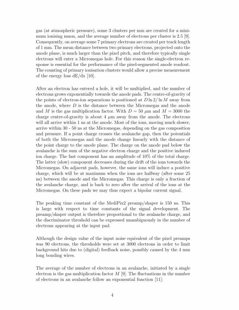
The average of the number of electrons in an avalanche, initiated by a singleelectron is the gas multiplication factor M [9]. The fluctuations in the numberof electrons in an avalanche follow an exponential function [11]:
4

p(n) = 1
Me−
n
M
where p(n) equals the probability to have an avalanche with n electrons intotal. The avalanche distribution is shown for several values of the gain M inFigure 5. Since the preamp noise is small with respect to the threshold, andsince there is no electron attachment, we apply the simple exponential distri-bution instead of approaches like the Polya distributions [12] which includeseveral 2nd order effects.
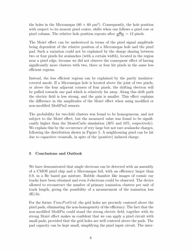
With a threshold set at T electrons, avalanches smaller than that are notdetected. The efficiency ǫ to detect single electrons is then given by:
ǫ = e−T
M
If, for instance, the threshold is set to a value that equals the gain, the efficiencyequals 1/e = 0.37. In Figure 6 the efficiency curve is depicted as a function ofthe gain M for a threshold T = 3000. We would like to keep the gas gain as lowas possible in order to a) limit the risk of discharges and ageing and b) limitthe ion space charge. With the present MediPix2, with its lowest threshold of3000 electrons, a gain of 10k would correspond to a single electron efficiencyof 0.74. For this reason we used He mixtures which allow a high gain, with asmall risk of discharges.
Due to discharges, four MediPix2 chips were destroyed within 24 hours ofoperation. The MediPix2 chip has no protection circuitry at its pixel inputpads other than the source and drain diffusions of the transistors responsiblefor leakage current compensation. We noticed some damage of the pixel pads,probably due to a high temperature in the discharge region. For InGrid,we intend to eliminate discharge damage by a) covering the bottom of theMicromegas with a (high) resistive layer, limiting the participating charge, b)covering the anode pads with a (high) resistive layer, in combination with c)a protective network, for each pixel, connected to the anode pad.
4 Results
4.1 Cosmic ray tracks and data readout; calibration
The MediPix2 sensor can be externally enabled and stopped, followed by areadout sequence in which the pixel counter data is transfered to a computer.We enabled the counters during an exposure time of 15 or 60 s, followed byrecording the image frame in the form of 65k counter contents. No trigger wasapplied.
5

The (positive) charge signals on the Micromegas were read out by means of alow-noise charge sensitive preamp, with a decay time constant of 1 µs. Signalsfrom an 55Fe source could be recorded, and the preamp was calibrated withcharge signals from a block wave, injected by means of a 10 pF capacitor.Together with the known number of primary electrons per 55Fe quantum, thegas amplification can be measured.
With a He/Isobutane 80/20 mixture, we observed signals from 55Fe events with−390 V on the Micromegas and −1000 V on the drift cathode plane. This isexpected given the large density of primary electrons in the interaction point[1] and the gain at this voltage of about 1k. We then increased the voltageon the Micromegas to −470 V, corresponding to a gain of approximately 19k.With a threshold setting of 3000 e−, we expect a single electron efficiency of0.85, and cosmic rays were observed.
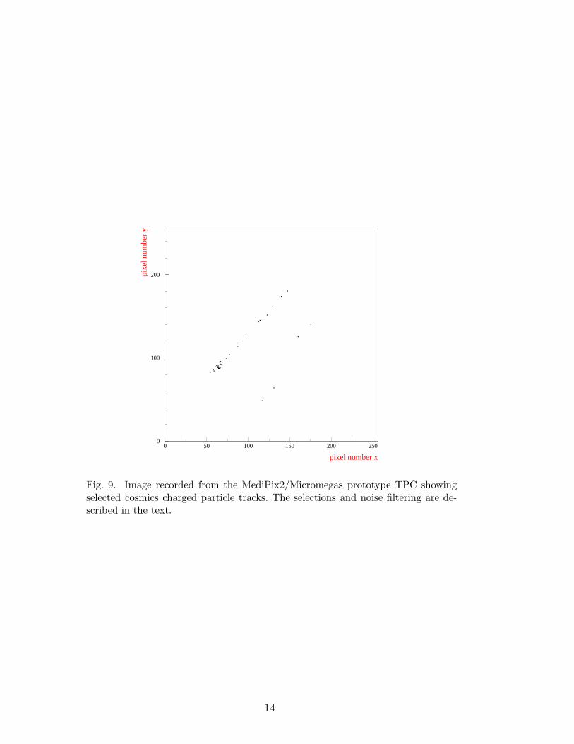
Some typical events are shown in Figures 7-9. Figure 7 shows a cosmic eventwith environmental background. Figure 8 shows a cosmic muon that knocksout a delta electron. Figure 9 shows a selected cosmic muon. The selectioncuts are described below. In this event the effect of diffusion can be observedin the spread of the hits along the track.
A selection to obtain a sample of clean cosmic events was made. For thedata a map of the noisy pixels was made. The signal from the edges and theinefficient upper left corner of the detector were removed. First, a straightline was searched using a Hough transform. Pixels within a distance of 20pixels are associated to the track. The following quantities were calculated:the number of associated pixels, the r.m.s. of the distance to the track, thetrack length in the detector plane Ld (in mm). The full 3D track length L
(in mm) is estimated as L =√
L2d+ 152. The track is split into two equal
parts and the minimum r.m.s. value of the two parts is calculated. Clustersare formed by stepping along the track and grouping all hits within a distanceof 5 pixels. The number of clusters is counted.
The following criteria were applied to select an event:
• the number of associated pixels larger than 5 and the fraction of associatedpixels to the track to the total number of pixels hit larger than 80%;
• Ld larger than 2.75 mm (i.e. 50 pixels);• the r.m.s. less than 4 ;• the number of associated pixels per millimeter of 3D track length should be
less than 4.
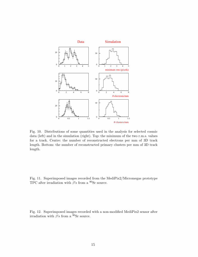
In total 164 events were selected in the data. The distributions of some physicalquantities are shown in Figure 10.
A simulation programme was written generating cosmic minimum ionising
6

particles with an angular distribution ∝ cos2 θ. The muon was tracked throughthe sensitive volume of the detector. Clusters were generated with an averageof 1.4 per mm and per cluster 3.16 electrons were generated using a Poissoniandistribution [13]. The electrons were drifted toward the MediPix2 detector witha diffusion constant of 220 µm per
√cm. Inefficient zones of the MediPix2
detector in the region between the pixels and below the pillars were put in.The detector is assumed to have an efficiency of 100% in the efficient zones.Note that multiple hits on a single pixel are at present not separated. Thesame selection cuts were applied to data and simulation.
The distribution of the minimum r.m.s. is sensitive to the diffusion constant.Data give an average value of 2.0 pixels (simulation 2.4). This implies thatthe diffusion constant is slightly better than 220 µm per
√cm. The observed
number of pixels hit per mm is 1.83 on average (2.70 simulation). The numberof clusters per mm is 0.52 (simulation 0.60). The average 3D track length is16.5 mm. The number of clusters per mm agrees within 15% with the sim-ulation, the number of electrons within 35%. Note that a 100% efficiency isassumed for the detector. Inefficiencies have also more impact on the numberof electrons than on the number of clusters. If we take into account system-atic uncertainties on the expected number of clusters and electrons per mm,uncertainties on the efficiency and operating conditions of the detector, wefind the agreement reasonable. Later experiments will focus on a more precisequantitative understanding of the detector.
4.2 Moire effects
Figure 11 shows an image, obtained after irradiating the chamber with β’sfrom a 90Sr source. The top-left corner of the image is clearly less efficient.This is due to the non-flatness of the Micromegas in its frame. Apparently,the electrostatic force could not entirely eliminate the warp in the Micromegasfoil. Here, the pillars are not in contact with the MediPix2 surface. The gap iswider and the gain is reduced. The dead regions due to the pillars are clearlyvisible as well.
Figure 12 shows the image, taken with a non-modified MediPix2 sensor, afterirradiating the drift volume with the 90Sr source. Band-shaped regions with areduced efficiency are clearly visible. Note that these bands are present in twoperpendicular directions. The same effect is visible in an image (Figure 13)which is the sum of all cosmic rays obtained during one night of data taking,again with a non-modified MediPix. The corresponding image from a modifiedMediPix2 is shown in Figure 14, where bands are still present, but much lesspronounced. The bands can well be explained in terms of a Moire effect: thepixel size of the MediPix2 sensor (55 × 55 µm2) does not match the pitch of
7
the holes in the Micromegas (60 × 60 µm2). Consequently, the hole positionwith respect to its nearest pixel centre, shifts when one follows a pixel row orpixel column. The relative hole position repeats after 60
60−55= 12 pixels.
The Moire effect can be understood in terms of the pixel signal amplitudebeing dependent of the relative position of a Micromegas hole and the pixelpad. Such a variation could not be explained by the charge sharing betweentwo or four pixels for avalanches (with a certain width), located in the regionnear a pixel edge, because we did not observe the consequent effect of havingsignificantly more clusters with two, three or four hit pixels in the same lessefficient regions.
Instead, the less efficient regions can be explained by the partly insulator-covered anode. If a Micromegas hole is located above the joint of two pixels,or above the four adjacent corners of four pixels, the drifting electron willbe pulled towards one pad which is relatively far away. Along this drift paththe electric field is less strong, and the gain is smaller. This effect explainsthe difference in the amplitudes of the Moire effect when using modified ornon-modified MediPix2 sensors.
The probability for two-fold clusters was found to be homogeneous, and notsubject to the Moire effect, but the measured value was found to be signifi-cantly higher than the MonteCarlo simulation (30% and 10%, respectively).We explain this by the occurrence of very large but not rare avalanche charges,following the distribution shown in Figure 5. A neighbouring pixel can be hitdue to capacitive crosstalk, in spite of the (positive) induced charge.
5 Conclusions and Outlook
We have demonstrated that single electrons can be detected with an assemblyof a CMOS pixel chip and a Micromegas foil, with an efficiency larger than0.9, in a He based gas mixture. Bubble chamber like images of cosmic raytracks have been obtained and even δ-electrons could be observed. The deviceallowed to reconstruct the number of primary ionisation clusters per unit oftrack length, giving the possibility of a measurement of the ionisation lossdE/dx.
For the future T imeP ixGrid, the grid holes are precisely centered above thepixel pads, eliminating the non-homogeneity of the efficiency. The fact that thenon-modified MediPix could stand the strong electric field, together with itsstrong Moire effect makes us confident that we can apply a pixel circuit withsmall pads, provided that the grid holes are well centered above the pads. Thepad capacity can be kept small, simplifying the pixel input circuit. The inter-
8
pad capacity is then also small, reducing the crosstalk between neighbouringpixels. A very small pad may reduce the maximum radiation dose, due toageing, and an optimum must be found.
The combination of a pixel sensor and a Micromegas offers an instrumentcapable to give a full 2D image of all single electrons in a gaseous volume.By replacing the MediPix2 sensor with a T imeP ix chip, a full 3D image isexpected to be within reach. These circuits will open new possibilities forparticle detection, in terms of position resolution, track separation and energyloss measurements. As an other example, the polarisation of X-ray quantacan be measured [14], after its interaction with gas, from the direction of thephoto-electron, which is registered accurately with the new device. Appliedwith a thin drift space of one mm, the device could be used as a fast vertexdetector in high radiation environments.
6 Acknowledgements
We thank the MediPix Collaboration for providing us with several wafers withMediPix2 chips, for the readout software and hardware. We would like to thankArnaud Giganon, Wim Gotink, Joop Rovekamp and Tom Aarnink for theircreative and essential contributions to the realisation of the test detectors.
References
[1] P. Colas, A.P. Colijn, A. Fornaini, Y. Giomataris, H. van der Graaf, E.H.MHeijne, X. Llopart, J. Schmitz, J. Timmermans and J.L. Visschers, Thereadout of a GEM or Micromegas equipped TPC by means of the MediPix2CMOS sensor as direct anode, Proceedings of the 10th Vienna Conference onInstrumentation, Vienna, Feb 2004, Submitted for publication in Nucl. Instr.and Methods
[2] Y. Giomataris et al., Micromegas: a high-granularity position-sensitive gaseousdetector for high particle-flux environments, Nucl. Instr. and Methods A 376(1996) 29-35
[3] X. Llopart, M. Campbell, R. Dinapoli, D. San Segundo and E. Pernigotti,MediPix2, a 64k pixel read-out with 55 µm square elements working in singlephoton counting mode, IEEE Trans. Nucl. Sci. 49 (2002) 2279-2283
[4] M. Conti, M. Maiorino, G. Mettivier, M. C. Montesi and P. Russo: Preliminarytest of Medisoft 4: control software for the MediPix2 readout chip, IEEE Trans.Nucl Sci. 50 (2003) 869-877
9

[5] D. San Segundo Bello, M. van Beuzekom, P. Jansweijer, H. Verkooijen andJ.L. Visschers, An interface board for the control and data acquisition of theMediPix2 chip, Nucl. Instr. and Methods A 509 (2003) 164-170
[6] Mesa+ Research Institute, University of Twente, The Netherlands.
[7] The Micromegas has been made by the CERN EST Workshop.
[8] Particle Data Group, Phys. Rev. D 66 (2002) 010001
[9] F. Sauli, Principles of operating of multiwire and proportional drift chambers,CERN Yellow Report 77-09, 1977.
[10] M. Hauschild, Proceedings of the International Workshop on Linear Colliders2002, Jeju, Korea, J.S. Kang and S.K. Oh (editors), 464-469
[11] H.S. Snyder, Phys. Rev. 72 (1947) 181
[12] W. Riegler, C. Lippmann, R. Veenhof, Detector physics and simulation ofresistive plate chambers, Nucl. Instr. and Methods A 500 (2003) 144-162
[13] S. Biagi, Monte Carlo simulation of electron drift and diffusion in counting gasesunder the influence of electric and magnetic fields, Nucl. Instr. and Methods A421 (1999) 234-240
[14] R. Bellazzini et al., Proceedings of the 10th Vienna Conference onInstrumentation, Vienna, Feb 2004, Submitted for publication in Nucl. Instr.and Methods, http://www.arxiv.org/physics/0403019
10

Fig. 1. Image acquired with the Medipix2/Micromegas prototype TPC [1].
MediPix2 pixel sensorBrass spacer blockPrinted circuit boardAluminum base plate
Micromegas
Cathode (drift) plane
55Fe
Baseplate
Drift space: 15 mm
Fig. 2. The layout of the chamber with the MediPix2, the Micromegas and the driftgap.
Fig. 3. The mounting of the Micromegas onto the MediPix2 sensor.
Fig. 4. The Medipix2 chip before (a) and after (b) the wafer post processing. Theoriginal pad (Al, 25 x 25 µm) is covered with an aluminum pad of 45 x 45 µm. Notethat no Micromegas mesh has yet been mounted on the chips shown in this figure.
11
Fig. 5. Probability distribution for the number of electrons in an avalanche forseveral values of the gas gain M .
Fig. 6. Single electron detection efficiency as a function of the gas gain for a thresh-old set at 3000 e−.
12

0
100
200
0 50 100 150 200 250
pixel number x
pix
el n
umbe
r y
Fig. 7. Image recorded from the MediPix2/Micromegas prototype TPC showingcosmics charged particle tracks together with some background. All the hit pixelsduring an acquisition time of 15 seconds are shown.
0
100
200
0 50 100 150 200 250
pixel number x
pix
el n
umbe
r y
Fig. 8. Image recorded from the MediPix2/Micromegas prototype TPC showing acosmic charged particle track together with a δ-electron.
13
0
100
200
0 50 100 150 200 250
pixel number x
pix
el n
umbe
r y
Fig. 9. Image recorded from the MediPix2/Micromegas prototype TPC showingselected cosmics charged particle tracks. The selections and noise filtering are de-scribed in the text.
14
Data Simulation
0
20
0 1 2 3 4 50
50
0 1 2 3 4 5
minimum rms (pixels)
0
20
0 2 4 6 80
50
0 2 4 6 8
# electrons/mm
0
20
0 0.5 1 1.50
50
0 0.5 1 1.5
# clusters/mm
Fig. 10. Distributions of some quantities used in the analysis for selected cosmicdata (left) and in the simulation (right). Top: the minimum of the two r.m.s. valuesfor a track. Centre: the number of reconstructed electrons per mm of 3D tracklength. Bottom: the number of reconstructed primary clusters per mm of 3D tracklength.
Fig. 11. Superimposed images recorded from the MediPix2/Micromegas prototypeTPC after irradiation with β’s from a 90Sr source.
Fig. 12. Superimposed images recorded with a non-modified MediPix2 sensor afterirradiation with β’s from a 90Sr source.
15

0
100
200
0 50 100 150 200 250
pixel number x
pix
el n
umbe
r y
Fig. 13. Superimposed images recorded with a non-modified MediPix2 sensor duringone night of cosmics data taking.
Fig. 14. Superimposed images recorded with a modified MediPix2 sensor duringone night of cosmics data taking.
16

This figure "fig1.jpeg" is available in "jpeg" format from:
http://arxiv.org/ps/physics/0409048

This figure "fig3.jpeg" is available in "jpeg" format from:
http://arxiv.org/ps/physics/0409048

This figure "fig11.jpeg" is available in "jpeg" format from:
http://arxiv.org/ps/physics/0409048

This figure "fig12.jpeg" is available in "jpeg" format from:
http://arxiv.org/ps/physics/0409048

This figure "fig14.jpeg" is available in "jpeg" format from:
http://arxiv.org/ps/physics/0409048


![arXiv:physics/0509066v1 [physics.optics] 8 Sep 2005](https://img.pdfslide.us/doc/110x75/628acd3388775e716a3cc184/arxivphysics0509066v1-8-sep-2005.jpg)


![arXiv:physics/0512190v1 [physics.optics] 21 Dec 2005](https://img.pdfslide.us/doc/110x75/6213b7afe848447ea44abf7d/arxivphysics0512190v1-21-dec-2005.jpg)