Embed Size (px)
Citation preview

c© 2017 Aarti Mahesh Kumar Shah

SUCCESSIVE-APPROXIMATION-REGISTER BASED QUANTIZERDESIGN FOR HIGH-SPEED DELTA-SIGMA MODULATORS
BY
AARTI MAHESH KUMAR SHAH
THESIS
Submitted in partial fulfillment of the requirementsfor the degree of Master of Science in Electrical and Computer Engineering
in the Graduate College of theUniversity of Illinois at Urbana-Champaign, 2017
Urbana, Illinois
Adviser:
Dr. Chandrasekhar Radhakrishnan

ABSTRACT
High-speed delta-sigma modulators are in high demand for applications such
as wire-line and wireless communications, medical imaging, RF receivers and
high-definition video processing. A high-speed delta-sigma modulator re-
quires that all components of the delta-sigma loop operate at the desired
high frequency. For this reason, it is essential that the quantizer used in
the delta-sigma loop operate at a high sampling frequency. This thesis
focuses on the design of high-speed time-interleaved multi-bit successive-
approximation-register (SAR) quantizers. Design techniques for high-speed
medium-resolution SAR analog-to-digital converters (ADCs) using synchronous
SAR logic are proposed.
Four-bit and 8-bit 5 GS/s SAR ADCs have been implemented in 65 nm
CMOS using 8-channel and 16-channel time-interleaving respectively. The
4-bit SAR ADC achieves SNR of 24.3 dB, figure-of-merit (FoM) of 638
fJ/conversion-step and 42.6 mW power consumption, while the 8-bit SAR
ADC achieves SNR of 41.5 dB, FoM of 191 fJ/conversion-step and 92.8 mW
power consumption. High-speed operation is achieved by optimizing the crit-
ical path in the SAR ADC loop. A sampling network with a split-array with
unit bridge capacitor topology is used to reduce the area of the sampling
network and switch drivers.
ii

To Mom, Dad and Pooja.
iii

ACKNOWLEDGMENTS
I would like to express my sincere gratitude to my adviser Dr. Chandrasekhar
Radhakrishnan without whose guidance and support this work would not
have been possible. His constant efforts to motivate and encourage me are
what have kept me on track these past two years. I am deeply grateful to
him for believing in me when I did not believe in myself and for always being
patient and understanding. He has played a fundamental role in my decision
to pursue graduate studies and I am thankful to him for always providing me
with the best opportunities. He has been an excellent mentor in matters of
both research and life. I would also like to thank his wife, Smitha, for all the
delicious meals and desserts she cooked for me and my group-mates during
my graduate studies.
I would also like to thank Dr. Bibhudatta Sahoo, my manager at XcelerICs
Inc., under whose guidance the work in chapters 5-7 was developed. I am
deeply grateful to him for providing me the opportunity to work at XcelerICs
Inc. and the invaluable lessons I have learned from him on integrated circuit
design. I take this opportunity to thank Dr. Pavan Kumar Hanumolu for his
guidance and for providing me the opportunity to interact with his research
group. I have greatly benefited from the technical expertise of him and his
students.
Words cannot express the role my family has played in my graduate studies
and in making me the person I am today. I am forever grateful to my family
for their unconditional love and support and all that they have done for
me throughout my life. Finally, I would like to thank my friends Snegha
Ramnarayanan, Varun Krishna, Shweta Patwa, Malak Shah, Linjia Chang,
Rishabh Poddar, Shashank Tandon, Pei Han Tsering, Mei Ling Yeoh, Ishita
Bisht and many others who made the bad times good and the good times
even better.
iv

TABLE OF CONTENTS
LIST OF TABLES . . . . . . . . . . . . . . . . . . . . . . . . . . . . . vii
LIST OF FIGURES . . . . . . . . . . . . . . . . . . . . . . . . . . . . viii
LIST OF ABBREVIATIONS . . . . . . . . . . . . . . . . . . . . . . . xi
CHAPTER 1 INTRODUCTION . . . . . . . . . . . . . . . . . . . . 11.1 Motivation . . . . . . . . . . . . . . . . . . . . . . . . . . . . . 11.2 Outline . . . . . . . . . . . . . . . . . . . . . . . . . . . . . . . 2
CHAPTER 2 DATA CONVERTERS OVERVIEW . . . . . . . . . . 32.1 Terminologies . . . . . . . . . . . . . . . . . . . . . . . . . . . 32.2 Sampling . . . . . . . . . . . . . . . . . . . . . . . . . . . . . . 42.3 Quantization . . . . . . . . . . . . . . . . . . . . . . . . . . . 42.4 Performance Metric of Data Converters . . . . . . . . . . . . . 92.5 Types of Data Converters . . . . . . . . . . . . . . . . . . . . 102.6 Analog-to-Digital Converter Architectures . . . . . . . . . . . 112.7 SAR ADC Topologies . . . . . . . . . . . . . . . . . . . . . . . 16
CHAPTER 3 DELTA-SIGMA DATA CONVERTERS . . . . . . . . . 183.1 Noise Shaping and First-Order ∆Σ Converters . . . . . . . . . 193.2 Second-Order ∆Σ Modulators . . . . . . . . . . . . . . . . . . 223.3 Higher-Order ∆Σ Modulators . . . . . . . . . . . . . . . . . . 23
CHAPTER 4 DELTA-SIGMA MODELING IN SIMULINK . . . . . 274.1 Simulink Modeling of First-Order ∆Σ Modulator . . . . . . . 274.2 Simulink Modeling of Second-Order ∆Σ Modulator . . . . . . 274.3 Simulink Modeling of Fifth-Order ∆Σ Modulator . . . . . . . 30
CHAPTER 5 HIGH-SPEED MULTI-BIT QUANTIZER DESIGN . . 335.1 Multi-phase Clock Generator . . . . . . . . . . . . . . . . . . . 345.2 4-bit SAR sub-ADC . . . . . . . . . . . . . . . . . . . . . . . 395.3 Simulation Results . . . . . . . . . . . . . . . . . . . . . . . . 48
CHAPTER 6 SAR ADC CRITICAL PATH ANALYSIS . . . . . . . 51
v

CHAPTER 7 SAR QUANTIZER PERFORMANCE ENHANCE-MENT . . . . . . . . . . . . . . . . . . . . . . . . . . . . . . . . . . 557.1 Multi-phase Clock Generator . . . . . . . . . . . . . . . . . . . 557.2 8-bit SAR sub-ADC . . . . . . . . . . . . . . . . . . . . . . . 567.3 Simulation Results . . . . . . . . . . . . . . . . . . . . . . . . 59
CHAPTER 8 CONCLUSION . . . . . . . . . . . . . . . . . . . . . . 65
REFERENCES . . . . . . . . . . . . . . . . . . . . . . . . . . . . . 66
APPENDIX A SIMULINK MODELS . . . . . . . . . . . . . . . . . . 70A.1 Second-order Delta-Sigma Modulator Simulink Models . . . . 70
APPENDIX B CADENCE SCHEMATICS . . . . . . . . . . . . . . . 72B.1 4-Bit SAR sub-ADC Schematics . . . . . . . . . . . . . . . . . 72B.2 8-channel Time-interleaved 4-Bit SAR ADC Schematics . . . . 79B.3 8-Bit SAR sub-ADC Schematics . . . . . . . . . . . . . . . . . 79B.4 16-channel Time-interleaved 8-Bit SAR ADC Schematics . . . 82
vi

LIST OF TABLES
4.1 Coefficients Used in the Single-bit MOD5 CIFB Structure . . 32
6.1 Critical Path Delays . . . . . . . . . . . . . . . . . . . . . . . 54
7.1 Power Breakdown . . . . . . . . . . . . . . . . . . . . . . . . . 627.2 Performance Comparison . . . . . . . . . . . . . . . . . . . . . 64
vii

LIST OF FIGURES
2.1 Additive Noise Model of a Quantizer . . . . . . . . . . . . . . 52.2 Probability Distribution of e[n] . . . . . . . . . . . . . . . . . 62.3 ADC Comparator Thresholds and DAC Output Levels for
a 4-level Mid-rise Quantizer . . . . . . . . . . . . . . . . . . . 82.4 ADC Comparator Thresholds and DAC Output Levels for
a 5-level Mid-tread Quantizer . . . . . . . . . . . . . . . . . . 82.5 A 2-bit Flash ADC . . . . . . . . . . . . . . . . . . . . . . . . 122.6 4-bit SAR ADC with Binary Weighted Capacitor Array . . . . 132.7 (a) A N-channel Time-interleaved ADC and (b) its Clock-
ing Sequence. . . . . . . . . . . . . . . . . . . . . . . . . . . . 152.8 4-bit Split-Array SAR ADC with Fractional Bridge Capacitor 172.9 4-bit Split-Array SAR ADC with Unit Bridge Capacitor . . . 17
3.1 (a) Discrete-Time First-Order (MOD1) Delta-Sigma Mod-ulator and (b) its Linear Model [1]. . . . . . . . . . . . . . . . 20
3.2 Discrete-Time Second-Order Delta-Sigma Modulator . . . . . 233.3 A 4th-order CIFB Structure . . . . . . . . . . . . . . . . . . . 253.4 A 4th-order CIFB Structure with Resonators . . . . . . . . . . 263.5 A 4th-order CRFB Structure . . . . . . . . . . . . . . . . . . . 26
4.1 Simulink Model of a MOD1 System . . . . . . . . . . . . . . . 274.2 Output Spectrum of a 5-bit MOD1 with OSR = 64 . . . . . . 284.3 Simulink Model of a MOD2 System . . . . . . . . . . . . . . . 284.4 Output Spectrum of a 5-bit MOD2 with OSR = 64 . . . . . . 294.5 Simulink Model of an 8-level Flash ADC . . . . . . . . . . . . 294.6 Simulink Model of an 8-level DAC . . . . . . . . . . . . . . . . 304.7 Simulink Model of a Single-bit 5th-order ∆Σ Modulator . . . . 314.8 Simulink Model of Loop Filter with CIFB Structure . . . . . . 314.9 Output Spectrum of a 1-bit MOD5 with OSR = 32 . . . . . . 32
5.1 CML-to-CMOS Circuit Schematic . . . . . . . . . . . . . . . . 355.2 Magnitude Response of First-stage Amplifier . . . . . . . . . . 365.3 Magnitude Response of Second-stage Amplifier . . . . . . . . . 365.4 Transient Response of CML-to-CMOS Converter . . . . . . . . 375.5 Johnson Counter with 8-phase Output . . . . . . . . . . . . . 38
viii

5.6 Eight Phases of the Sampling Clock . . . . . . . . . . . . . . . 385.7 Current Mode Logic based D-latch . . . . . . . . . . . . . . . 395.8 D Flip-flop with Asynchronous Reset . . . . . . . . . . . . . . 395.9 Clocks Used in the SAR sub-ADC . . . . . . . . . . . . . . . . 405.10 The Pre-amplifier . . . . . . . . . . . . . . . . . . . . . . . . . 415.11 Frequency Response of the Pre-amplifier . . . . . . . . . . . . 425.12 The StrongARM Latch . . . . . . . . . . . . . . . . . . . . . . 435.13 The Set-Reset Latch . . . . . . . . . . . . . . . . . . . . . . . 435.14 Single-ended 4-bit SAR Sampling Network Implementation . . 445.15 2-bit SAR Logic Block and relevant Timing Sequence . . . . . 455.16 4-bit SAR Logic Block . . . . . . . . . . . . . . . . . . . . . . 465.17 Custom Set-Reset D Flip-flop . . . . . . . . . . . . . . . . . . 465.18 Custom Set-Reset D Flip-flop . . . . . . . . . . . . . . . . . . 475.19 Output Spectrum of the 4-bit SAR Sub-ADC Using a Low-
Frequency Input Signal . . . . . . . . . . . . . . . . . . . . . . 485.20 Output Spectrum of the 4-bit SAR Sub-ADC Using a High-
Frequency Input Signal . . . . . . . . . . . . . . . . . . . . . . 495.21 Low-Frequency Output Spectrum of 8-channel Time-interleaved
SAR ADC . . . . . . . . . . . . . . . . . . . . . . . . . . . . . 505.22 High-Frequency Output Spectrum of 8-channel Time-interleaved
SAR ADC . . . . . . . . . . . . . . . . . . . . . . . . . . . . . 50
6.1 The SAR Loop . . . . . . . . . . . . . . . . . . . . . . . . . . 516.2 A 2-bit SAR Logic Block . . . . . . . . . . . . . . . . . . . . . 526.3 Timing Diagram of 2-bit SAR Logic Block with Critical
Path Delays . . . . . . . . . . . . . . . . . . . . . . . . . . . . 53
7.1 16-phase Johnson Counter . . . . . . . . . . . . . . . . . . . . 567.2 16 Phases of the Sampling Clock . . . . . . . . . . . . . . . . 567.3 Single-ended 8-bit SAR Sampling Network Implementation . . 587.4 8-bit SAR Logic Block . . . . . . . . . . . . . . . . . . . . . . 587.5 Low-Frequency Output Spectrum of the 8-Bit SAR sub-
ADC Using Ideal and Real Switches . . . . . . . . . . . . . . . 607.6 Output Spectrum of the 8-bit SAR Sub-ADC Using a High-
Frequency Input Signal . . . . . . . . . . . . . . . . . . . . . . 617.7 Low-Frequency Output Spectrum of 16-channel Time-interleaved
SAR ADC . . . . . . . . . . . . . . . . . . . . . . . . . . . . . 637.8 High-Frequency Output Spectrum of 16-channel Time-interleaved
SAR ADC . . . . . . . . . . . . . . . . . . . . . . . . . . . . . 63
A.1 Simulink Model of 33-level Flash ADC . . . . . . . . . . . . . 70A.2 Simulink Model of 33-level DAC . . . . . . . . . . . . . . . . . 71
B.1 CML D-Latch . . . . . . . . . . . . . . . . . . . . . . . . . . . 72B.2 Top-level Test-bench Schematic for 4-bit SAR ADC . . . . . . 73
ix

B.3 8 Phase Clock Generator . . . . . . . . . . . . . . . . . . . . . 73B.4 Clocks for 4-Bit SAR . . . . . . . . . . . . . . . . . . . . . . . 74B.5 4-bit SAR ADC . . . . . . . . . . . . . . . . . . . . . . . . . . 74B.6 4-bit Differential SAR Sampling Network . . . . . . . . . . . . 75B.7 Differential Half-circuit of 4-bit SAR Sampling Network . . . . 75B.8 The Comparator Block . . . . . . . . . . . . . . . . . . . . . . 75B.9 The Pre-amplifier . . . . . . . . . . . . . . . . . . . . . . . . . 76B.10 The Comparator-latch . . . . . . . . . . . . . . . . . . . . . . 76B.11 4-bit SAR Logic Block . . . . . . . . . . . . . . . . . . . . . . 77B.12 D Flip-flop with Asynchronous Reset . . . . . . . . . . . . . . 77B.13 D Flip-flop with Asynchronous Set . . . . . . . . . . . . . . . 78B.14 D Flip-flop with Asynchronous Set-Reset . . . . . . . . . . . . 78B.15 Top-level Test-bench Schematic for 8-channel Time-interleaved
4-bit SAR ADC . . . . . . . . . . . . . . . . . . . . . . . . . . 79B.16 Top-level Test-bench Schematic for 8-bit SAR ADC . . . . . . 79B.17 Clocks for 8-bit SAR ADC . . . . . . . . . . . . . . . . . . . . 80B.18 8-bit SAR sub-ADC . . . . . . . . . . . . . . . . . . . . . . . 80B.19 8-bit SAR Sampling Network . . . . . . . . . . . . . . . . . . 80B.20 Differential Half-circuit of 8-bit SAR Sampling Network . . . . 81B.21 8-bit SAR Logic Block . . . . . . . . . . . . . . . . . . . . . . 81B.22 Top-level Test-bench Schematic for 16-channel Time-interleaved
8-bit SAR ADC . . . . . . . . . . . . . . . . . . . . . . . . . . 82
x

LIST OF ABBREVIATIONS
∆Σ Delta-Sigma
ADC Analog-to-Digital Converter
A/D Analog-to-Digital
CIFB Cascade of integrators with distributed feedback and distributedinput coupling
CML Current-Mode-Logic
CMOS Complementary metal-oxide semiconductor
CRFB Cascade of resonators with distributed feedback and distributedinput coupling
D/A Digital-to-Analog
DAC Digital-to-Analog Converter
DFF D Flip-flop
DFFR D Flip-flop with asynchronous reset
DFFS D Flip-flop with asynchronous set
DFFSR D Flip-flop with asynchronous set-reset
DLL Delay-locked Loop
FFT Fast Fourier Transform
FoM Figure-of-merit
LSB Least Significant Bit
MOD1 First-order Delta Sigma Modulator
MOD2 Second-order Delta Sigma Modulator
xi

MOD5 Fifth-order Delta Sigma Modulator
MPCG Multi-phase Clock Generator
NTF Noise Transfer Function
OpAmp Operational Amplifier
OSR Oversampling Ratio
SAR Successive Approximation Register
SFDR Spurious-Free Dynamic Range
SNDR Signal-to-Noise and Distortion Ratio
SNR Signal-to-Noise Ratio
SQNR Signal-to-Quantization Noise Ratio
STF Signal Transfer Function
TI Time-interleaved
xii

CHAPTER 1
INTRODUCTION
1.1 Motivation
Analog-to-digital converters form the basis of any signal processing system
that interacts with the real world. Advances in design of signal process-
ing systems such as wireless and wireline communications, software defined
radio, Ethernet and high-definition video processing have been made pos-
sible through advances in designs of analog-to-digital converters. In recent
years the increased demand for higher bandwidths of analog-to-digital con-
verters (ADCs) has spurred further research in developing high-speed ADCs
[2],[3],[4].
High-speed delta-sigma modulators are in high demand in applications
such as wire-line and wireless communications, medical imaging and RF
receivers [2],[3],[4]. A high-speed delta-sigma modulator requires that all
components of the delta-sigma loop are able to operate at the desired high
frequency. For this reason, it is essential that the quantizer used in the
delta-sigma loop is able to operate at a high sampling frequency.
In this thesis we focus on the design of a high-speed time-interleaved multi-
bit successive approximation based quantizer designed to operate at a sam-
pling rate of 5GS/s. High-speed quantizers with 4-8 bit precision operat-
ing in the GHz range are nearly impossible to build using a single chan-
nel. Therefore, time-interleaved ADCs consisting of several slow sub-ADCs
are needed to achieve such high sample rates, thereby increasing the total
area. Successive-approximation-register (SAR) based ADCs are ideal for this
application as they consist of mainly digital components that benefit from
technology scaling in low-voltage CMOS processes and thus provide a high
speed-to-area ratio [5]. A SAR quantizer can also provide better performance
compared to other quantizers when used in a delta-sigma loop by providing
1

an extra order of noise-shaping. The successive approximation process gen-
erates a residue voltage on the charge re-distribution capacitor that can be
exploited as the quantization error required for the delta-sigma modulator
[6],[7].
1.2 Outline
This thesis is organized into seven chapters. Chapter 2 provides an introduc-
tion to analog-to-digital converters (ADC) and describes some key concepts
used in the thesis. Chapter 3 provides a brief introduction the delta-sigma
modulation and explains the working of some commonly used delta-sigma
modulators. Chapter 4 presents the SIMULINK implementations of a first-,
second- and fifth-order delta-sigma modulator. Chapters 5, 6 and 7 form the
heart of this thesis. Chapter 5 explains the design of the 8-channel time-
interleaved 4-bit 5GS/s successive approximation register (SAR) based ADC
implemented in 65 nm CMOS. Chapter 6 provides an analysis of the critical
contributors to delays in the SAR ADC loop. Chapter 7 discusses the archi-
tecture of the proposed 16-channel time-interleaved 8-bit 5GS/s ADC and
optimum choices to be made while designing high-speed medium-resolution
SAR ADCs. Finally, we conclude the thesis in chapter 8. Simulink models
of the delta-sigma modulators implemented and transistor-level schematics
of the SAR ADCs have been included in the appendices.
2

CHAPTER 2
DATA CONVERTERS OVERVIEW
Analog-to-digital converters (ADCs) are at the heart of any electronic system
that interacts with the real world. The real world we live in is made of
analog signals such as speech, medical imaging, sonar, radar, etc., i.e. signals
that are continuously varying with time [8]. An analog-to-digital converter
converts analog signals to digital signals, i.e. signals that exist for discrete
instances of time and that have only certain discrete values. In this way an
ADC enables us to convert an infinite signal into a finite signal without loss
of significant information, enabling us to process this finite data for various
applications. Analog-to-digital converters are critical to signal processing
systems such as RF receivers, Ethernet, wireless communication, software-
defined radio etc.
This chapter briefly explains the process of analog-to-digital conversion,
some commonly used terminology in ADC design as well as the metrics used
to evaluate the performance of an ADC. This chapter also describes two dif-
ferent types of commonly used data converters and explains the architecture
of different ADCs and digital-to-analog converters (DACs).
2.1 Terminologies
2.1.1 Analog Signal
An analog signal is a signal that can take any value and is defined for all
instances of time (t). An analog signal can have infinite values and infinite
precision [9]. An analog signal is also known as a continuous-time analog
signal.
3

2.1.2 Discrete-time Signal
A discrete-time signal is a signal that can take any value but is defined only
for discrete instances of time (n) [9].
2.1.3 Digital Signal
A digital signal is a signal that is discrete in terms of both time and ampli-
tude. That is, it exists only for discrete instances of time and can only take
discrete values of the form k∆, where k is an integer and ∆ is a fixed value.
2.2 Sampling
Sampling is the process of discretization of time, by which a continuous-
time analog signal is converted into a discrete-time signal. Sampling enables
us to represent a signal consisting of infinitely many points using a finite
number of points, and thereby store the data in finite-memory devices such
as computers and other electronics. The original signal can be perfectly
reconstructed from a sampled signal as long as the sampling criterion given
by (2.1) is satisfied. The sampling criterion states that a band-limited signal
can be perfectly reconstructed as long as the sample rate (fs) is twice its
bandwidth (fb). This is known as the Shannon-Nyquist sampling theorem.
fs ≥ 2× fb (2.1)
Sampling is usually the first stage in the analog-to-digital conversion process.
The amplitude of the continuous-time signal is first sampled onto a capacitor
after which it is quantized using a quantizer.
2.3 Quantization
The process of analog-to-digital conversion of a continuous-time signal can
be decomposed into two main parts - quantization of time, better known
as sampling, and quantization of the amplitude of the time-varying signal,
commonly known as quantization. Quantization is the process by which a
4

sampled value can be represented by a binary word of a fixed length [10]. A
quantizer maps a large set of input values to a smaller set [11]. Quantization is
thus basically just the process of approximating an input value. The accuracy
with which the quantized value matches the original input depends on the
precision of the quantizer, i.e., its number of levels. The number of levels in
a quantizer is usually defined as a power of 2, thus a B-bit quantizer consists
of 2B levels. The quantized value is usually represented by a digital code in
binary as a one’s or two’s complement number. Quantization can be of two
types based on the number of quantization levels – midtread quantization
or midrise quantization. These are explained in detail in sections 2.3.2 and
2.3.1.
The approximating nature of quantization degrades the input signal. The
difference between the quantized sample, v[n], and the input sample, u[n], is
known as the quantization error or quantization noise, e[n].
e[n] = v[n]− u[n] (2.2)
A quantizer can thus be represented by its additive noise model (Fig. 2.1)
where the quantized output, v[n], is given by (2.3) [11].
e[n]
u[n] v[n]
Figure 2.1: Additive Noise Model of a Quantizer
v[n] = u[n] + e[n] (2.3)
The statistical model of a quantizer assumes that the quantization noise
is a sample sequence of a wide-sense stationary white noise process, i.e. it is
uncorrelated with the input and the probability distribution of the quanti-
zation error is uniform [11]. These assumptions of the statistical model are
only valid when the quantizer is not overloaded, the input signal is complex
and the quantization steps are small [11].
5
A quantizer is said to be overloaded when the input exceeds the full-scale
range, (Rfs), of the quantizer. The full-scale range of a quantizer is predefined
by its circuit design. The input is usually scaled down to ensure that it is
within the full scale range of the quantizer, given by (2.4), where Vref is a
chosen reference voltage.
Rfs = 2× Vref (2.4)
The smallest quantization level or minimum step-size, ∆, of a B bit quantizer
is given by (2.5). This is also commonly referred to as the least-significant
bit (LSB) since a change in the input corresponding to ∆ changes the LSB
of the binary coded output [10].
∆ =Rfs
2B=
2Vref2B
=Vref2B−1
(2.5)
The quantization error, e[n], of a quantizer with step-size ∆ is bounded by
(2.6) as long as the input is within the full-scale range of the quantizer. When
the input is outside the full-scale range of the quantizer the quantization error
increases linearly with magnitude of the input and the quantized output is
clipped to the maximum quantization level [11].
−∆
2≤ e[n] ≤ ∆
2(2.6)
Since the quantization error, e[n], is assumed to be a white noise process
it has a uniform probability distribution. The probability distribution of e[n]
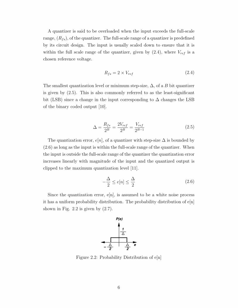
shown in Fig. 2.2 is given by (2.7).
2 2e
P(e)
1
Figure 2.2: Probability Distribution of e[n]
6
P (e[n]) =
1∆−∆
2≤ e[n] ≤ ∆
2
0 else(2.7)
The quantization noise power of the quantization error is given by its
variance given by (2.8).
Pe =
∫ ∞−∞
e2 · P (e) de
=
∫ ∆2
−∆2
e2
∆de
=∆2
12
(2.8)
Since the quantization error sequence is white, power spectral density1,
Se(ω), is white as well, i.e. it is uniformly distributed over all frequencies
and its power is within ±π. The height of the one-sided power spectral
density, ke, of the quantization noise can be found from its noise power and
is given by (2.10) [12].
Pe =
∫ π
0
S2e (ω) dω = πk2
e =∆2
12(2.9)
ke =∆√12π
(2.10)
Therefore, the one-sided power spectral density of the quantization error,
Se(ω), is given by (2.11).
Se(ω) =
∆√12π
0 ≤ ω ≤ π
0 else(2.11)
2.3.1 Mid-rise Quantization
Mid-rise quantization is used when the number of levels in the required quan-
tizer is even, i.e. it can be represented as a power of 2. Analytically, the
1The discrete-time angular frequency ω = ΩTs = 2π ffs
, where Ω – the continuous-timeangular frequency, fs – the sampling frequency and f – the continuous-time frequency.
7
output of a mid-rise quantizer, v[n], can be represented in terms of the input
to the quantizer, u[n], and the quantization step-size ∆ by (2.12) [10].
v[n] = ∆
⌊u[n]
∆+
1
2
⌋(2.12)
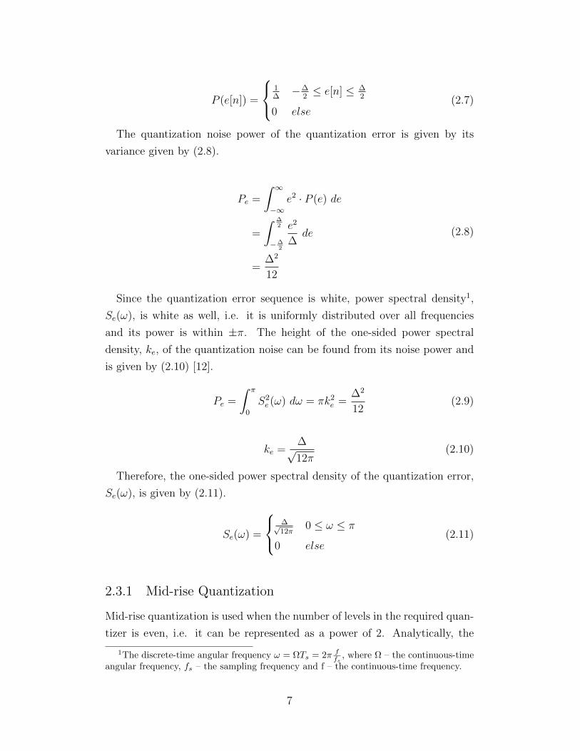
Figure 2.3 shows the number line from −VR to VR with the ADC compara-
tor threshold voltages and DAC output voltages marked for a 4-level (i.e.
2-bit) mid-rise quantizer. Here, VR is the reference voltage of the quantizer.
VRVR
ADC Thresholds
DAC Levels
Figure 2.3: ADC Comparator Thresholds and DAC Output Levels for a4-level Mid-rise Quantizer
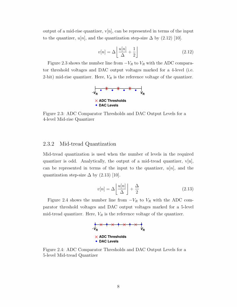
2.3.2 Mid-tread Quantization
Mid-tread quantization is used when the number of levels in the required
quantizer is odd. Analytically, the output of a mid-tread quantizer, v[n],
can be represented in terms of the input to the quantizer, u[n], and the
quantization step-size ∆ by (2.13) [10].
v[n] = ∆
⌊u[n]
∆
⌋+
∆
2(2.13)
Figure 2.4 shows the number line from −VR to VR with the ADC com-
parator threshold voltages and DAC output voltages marked for a 5-level
mid-tread quantizer. Here, VR is the reference voltage of the quantizer.
VRVR
ADC Thresholds
DAC Levels
Figure 2.4: ADC Comparator Thresholds and DAC Output Levels for a5-level Mid-tread Quantizer
8

2.4 Performance Metric of Data Converters
2.4.1 Signal-to-Quantization Noise Ratio
The performance of an ADC is measured by comparing the power due to
the input signal content and the power due to the noise content in the quan-
tized output. The ratio of the signal power to the quantization noise power
is known as the signal-to-quantization noise Ratio (SQNR). The SQNR of
a signal is usually expressed in decibels (dB). The power of a sine wave
of full-scale amplitude A = Vref is given by (2.14) while the power of the
quantization noise is given by (2.8).
Psig =A2
2=V 2ref
2=
2B−1∆2
2(2.14)
The SQNR of the output signal of a uniform B bit quantizer with input
power Psig and quantization noise power Pe is given by (2.15). Thus, it can
be seen that the SQNR increases by 6 dB per bit.
SQNR = 10 log10
(PsigPe
)= 6.02B + 1.76 [dB]
(2.15)
2.4.2 Spurious-Free Dynamic Range
The performance of an analog-to-digital converter is also commonly measured
using its spurious-free dynamic range (SFDR). The SFDR of a signal is the
ratio of the power due to its input signal to the power of the largest distortion
component (known as a spurious tone or spur) in the spectrum. The SFDR
of a signal is given by (2.16).
SFDR = 10 log10
(PsigPspur
)(2.16)
The SFDR of a uniform B bit quantizer for a sinusoidal input can be
approximated using (2.17) [13].
9

SFDR = 8.07B + 3.29 [dB] (2.17)
2.5 Types of Data Converters
Data converters (ADCs and DACs) are categorized into two broad categories,
Nyquist-rate converters or oversampling converters, based on the relationship
between the frequency of the input signal, fin, and the sampling rate of the
data converter, fs.
2.5.1 Nyquist-rate Converters
Data converters in which the input signal is sampled at a frequency close to
the Nyquist-rate are known as Nyquist-rate converters. Usually, Nyquist-rate
converters operate at 1.5 to 10 times the Nyquist-rate [12]. The quantization
error in Nyquist-rate converters has a flat-band spectrum, i.e. the quantiza-
tion noise is uniformly distributed among all frequencies.
2.5.2 Oversampling Converters
Oversampling converters are data converters that operate at a much higher
frequency than the Nyquist-rate of the input signal. Oversampling converters
are used when the input signal is bandlimited, i.e. all signals of interest are
below some frequency, fb, known as the bandwidth of the input signal. The
oversampling ratio of a data converter is given by (2.18).
OSR =fs2fb
(2.18)
Oversampling converters operate at oversampling ratios (OSR) of about
10 to 512. Oversampling converters are used to increase the SNR of the
output of an ADC. The input is first sampled and quantized at a rate much
higher than the Nyquist-rate. A high sampling frequency, fs, causes the
quantization noise to be spread over a larger frequency range (0 to fs/2).
Since all signals of interest are below fb, the signals and quantization noise
10

outside the signal’s bandwidth are then filtered out using a digital or analog
filter [12]. This elimination of the out-of-band quantization noise improves
the SNR of the output signal. If the filter used is a brick wall filter with
transfer function, H(ω), given by (2.19), the new quantization noise power,
Pe, of the filtered signal is given by (2.20) [12].
|H(ω)| =
1 − πOSR≤ ω ≤ π
OSR
0 else(2.19)
Pe =
∫ πOSR
0
S2e (ω) · |H(ω)|2 dω =
∆2
12
(1
OSR
)(2.20)
Therefore, the SQNR of a B-bit oversampling converter for a sine input is
given by (2.21).
SQNR = 10 log10
(PsigPe
)= 6.02B + 1.76 + 10 log(OSR) [dB]
(2.21)
Increasing the OSR by two times gives a 3 dB improvement in SNR or,
equivalently, improves the performance by 0.5 bits [12]. Most commonly, the
SNR of oversampling converters is further improved by reducing the in-band
quantization noise using noise-shaping as in delta-sigma converters. Delta-
sigma converters are explained in detail in chapter 3.
2.6 Analog-to-Digital Converter Architectures
In this section, three different types of ADCs — flash ADC, SAR ADC and
time-interleaved (TI) ADC — relevant to this thesis are described. The flash
ADC is used as the quantizer in the delta-sigma simulink models in chapter
4, while SAR ADCs and TI ADCs are designed in chapters 5 and 7.
2.6.1 Flash Converters
Flash ADCs have the simplest and best architecture for very high-speed
analog-to-digital conversion [14],[12]. A flash ADC consists of comparators
and a resistor ladder. The input signal is fed to an array of comparators
11

and compared to a set of known references voltages generated by the resistor
ladder. If the input of the comparator is greater than the reference voltage,
then its output is set to 1, otherwise it is set to 0. The comparator outputs
thus represent the input in a digital thermometer code which can be converted
into a binary code using a decoder. Figure 2.5 shows the architecture of
a 2-bit flash ADC. The flash converter thus has a very simple structure
and can achieve high speeds as the input is processed by comparators in
parallel. However, flash converters are not hardware efficient; a flash ADC
requires 2N − 1 comparators to achieve N -bit resolution [14]. The number of
comparators thus grows exponentially with resolution which results in large
power consumption and area for resolutions above 8 bits [15].
Vin
R
R
R
R
2−bits
D
COD
E
ER
Digital
Output
VR
VR
Figure 2.5: A 2-bit Flash ADC
2.6.2 Successive Approximation Converters
Successive approximation converters are widely used in applications where
high-accuracy analog-to-digital (A/D) conversion is desired [12]. A basic
successive approximation converter consists of a comparator, a successive ap-
proximation register (SAR) and a DAC [14]. These converters are commonly
known as SAR ADCs. A SAR ADC performs a “binary search” algorithm on
the input using a feedback loop. The binary search algorithm uses a divide-
and-conquer strategy to find the location of a number in a sorted array. A
binary search divides the search space into two each time [12]. Consider an
input Vx and a reference voltage VR. The initial search space consists of all
12

voltages from 0 to VR. The algorithm first checks whether Vx > VR/2 or
Vx < VR/2. If Vx > VR/2, then the next search space is from VR/2 to VR; if
not, then the next search space is from 0 to VR/2. This process of dividing
the search space is performed N times in an N-bit ADC. This algorithm thus
brings the quantized output within 1 LSB of the input signal. An N bit SAR
ADC requires N clock cycles to complete an N-bit conversion.
Figure 2.6 shows a 4-bit SAR ADC. The working of a SAR ADC consists of
two phases: a sampling phase and a bit-cycling phase. During the sampling
phase, the input signal is sampled onto the sampling network. A binary
weighted capacitive DAC (CDAC) is used as the sampling network in Fig.
2.6. Two other sampling network topologies — split-array with fractional
bridge capacitor and split-array with unit bridge capacitor — are explained
in sections 2.7.2 and 2.7.3. The sampled value, Vx, is fed as input to the
comparator during the bit-cycling phase. The output of the comparator,
Vcomp, is fed to the successive approximation register (also known as SAR
logic block) which sets the value of the desired bit. At the end of the bit-
cycling phase the bits b4b3b2b1b0 are set to the quantized value.
C 8C4C2CC
inV
Vx
Vcomp
S
S 1 S S S S2 3 4 5
6
RV0b RVb RVb RVb RVb1 2 3 4
Figure 2.6: 4-bit SAR ADC with Binary Weighted Capacitor Array
During the sampling phase, the switches S1−S5 are connected to the input,
Vin, to sample the input signal onto the CDAC and switch S6 is closed,
grounding the node Vx. The charge on the sampling network during the
sampling phase, QS, is given by (2.22).
QS = −16C × Vin (2.22)
At the start of the bit-cycling phase the MSB, b4, is set to 1 while bits
b3− b0 are set to 0. Switch S5 is thus connected to the reference voltage, VR,
while the switches S1 − S4 are connected to ground. During the bit-cycling
phase switch S6 is open. The charge on the sampling network during the
13

bit-cycling phase, QH , is given by (2.23).
QH = −Vx × 16C + (VR − Vx)× 16C (2.23)
By principle of charge conservation the total charge of the sampling network
during the two phases remains the same, i.e., QS = QH . Therefore, the
voltage on node Vx during the bit-cycling phase is given by (2.24). If Vin >
VR/2, Vcomp = 1 and b4 is set to 1, else b4 is set to one. During the next clock
cycle, the b3 is set to 1 and the value of Vx is re-evaluated to set the value of
b3. This process goes on until all the bits are set.
Vx =VR2− Vin (2.24)
SAR ADCs are widely used as they comprise mainly digital components.
SAR ADCs thus largely benefit from technology scaling and provide a small-
area and low-power solution — attributes that are highly desirable.
2.6.3 Time-interleaved Converters
Very high-speed ADCs can be realized by operating multiple ADCs in paral-
lel where each ADC operates at a much lower speed. The different sub-ADCs
operate on different phases of the clock, ensuring that each ADC acts on a dif-
ferent sample. An N-channel time-interleaved ADC consists of N sub-ADCs
operating on clock phases separated by 2π/N . Each sub-ADC operates at a
frequency of fs/N . The quantized outputs from each channel are inter-leaved
using a multiplexer, giving an output produced at an effective frequency of fs.
Figure 2.7 shows an N -channel time-interleaved ADC and its corresponding
clocking sequence.
The performance of a time-interleaved ADC can be highly degraded if there
are mismatches among the different channels. Mismatches in timing, gain,
and offset can give rise to higher noise power in the output [15]. Mismatches
among the different channels can produce inter-modulation products of the
input in the output spectrum, thereby increasing the noise in the spectrum.
If the source of the mismatches is known, then these can be corrected by
digital filtering [12].
14

IGITAL
D
MUX
ADC 1
inV Digital
Output
S/H
ADC NS/H
Φ1
ADC 2S/H
Φ
ΦN
2
N−bits
(a)
Φ
t
Φ
CK
1
Φ2
ΦN
CKNT
(b)
Figure 2.7: (a) A N-channel Time-interleaved ADC and (b) its ClockingSequence.
15

2.7 SAR ADC Topologies
Various CDAC topologies can be used to implement the sampling network
for a SAR ADC. Three SAR ADC topologies are discussed in this section.
2.7.1 Binary Weighted Capacitor Array
The binary weighted capacitor-array for an N-bit SAR ADC uses n+1 ca-
pacitors with the weight of the largest capacitor being 2N times that of the
unit capacitor. As the number of ADC bits, N , increases this results in the
load capacitor size and area of the chip increasing exponentially [16]. Figure
2.6 shows a 4-bit binary weighted SAR ADC.
2.7.2 Split-Array SAR ADC with Fractional Bridge Capacitor
The issue of increased area and capacitance posed by a binary weighted
capacitor array can be solved by using a split capacitor DAC. Figure 2.8
shows a 4-bit design of a split capacitor DAC. This design consists of two
capacitor arrays - the LSB side (left) and the MSB (right) side - separated by
a bridge capacitor connected in series between them. The size of the bridge
capacitor is given by (2.25).
Cb =Ctotal of LSB array
Ctotal of MSB array(2.25)
Therefore, in Fig. 2.8, the value of the bridge capacitor is given by Cb = 4C3C
.
The effective capacitance of the LSB side and the bridge capacitor is C;
therefore, the total capacitance of the sampling network is given by 4C. The
total capacitance of the sampling network is thus significantly reduced for an
N-bit SAR ADC. This topology is thus very useful as the resolution of the
ADC increases. A fractional capacitor, however, results in poor matching
with the other capacitors and thus in erroneous values. The bridge capacitor
also suffers due to the parasitic effects due to the top and bottom plate
capacitances.
16

C 2CC
inV
S 1 S S2 3
Vx
S S4 5
Cb
Vcomp
S 6C 2C
RVb RVb RVb RVb0 1 2 3
Figure 2.8: 4-bit Split-Array SAR ADC with Fractional Bridge Capacitor
2.7.3 Split-Array SAR ADC with Unit Bridge Capacitor
Figure 2.9 shows a 4-bit split-array SAR ADC using a unit capacitor. The
issue of poor matching in the the split-array SAR in section 2.7.2 can be
resolved by replacing the fractional bridge capacitor with a unit capacitance
and removing the dummy capacitor in the LSB array. This solution in-
troduces a 1 LSB gain error but solves the issue of matching [16]. This
structure too is vulnerable to the parasitic capacitance effects introduced by
the top and bottom capacitance of the bridge capacitor, thereby causing a
mismatch between the LSB and MSB array, thereby degrading the overall
ADC performance [16]. However, the effects of the parasitic capacitance are
not significant in medium resolution (6−8 bit) ADCs. Therefore, this topol-
ogy provides reduced area with acceptable performance and is an optimum
solution for medium resolution ADCs.
Vcomp
2CC 2CC
C
S S S S
S
Vx
1 2 3 4
5
inV
RVb RVb0 1 RVb2 RVb3
Figure 2.9: 4-bit Split-Array SAR ADC with Unit Bridge Capacitor
17

CHAPTER 3
DELTA-SIGMA DATA CONVERTERS
Delta-sigma (also known as sigma-delta) data converters are a type of over-
sampled data converters [17]. Delta-sigma data converters greatly enhance
the SNR that can be achieved by oversampled converters. Thus they are
extremely useful in modern voiceband, audio, and high-resolution precision
industrial measurement applications that require high accuracy, up to 15-20
bits and fairly high speeds of operation (8 - 500 kS/s) [18],[19]. As mentioned
in chapter 2, section 2.5.2, oversampled converters increase the performance
of the ADC by sampling the input at a much higher frequency than the
Nyquist frequency and then filtering out the signal within the desired fre-
quency bandwidth [20]. This in turn filters out the out-of-band quantization
noise thereby increasing SQNR performance. The basic idea behind a delta-
sigma converter is that the SQNR performance of an ADC can be further
improved if the in-band quantization noise of the oversampling converter can
be reduced. This can be achieved using a technique called noise shaping,
further explained in section 3.1.
A delta-sigma converter consists of three main components - an ana-
log/digital filter (also known as the modulator/loop filter), a low-resolution
quantizer and a DAC in a feedback loop [1]. Delta-sigma converters enable us
to obtain a high-resolution ADC while using a quantizer with a much lower
resolution [21]. Delta-sigma modulators can be of two types - continuous-
time ∆Σ converters that use analog filters, or discrete-time ∆Σ converters
that use digital filters. This work focuses on discrete-time ∆Σ converters.
Various discrete-time ∆Σ converters are implemented in Simulink in chap-
ter 4, while chapters 5-7 focus on the design of a high-speed quantizer for a
high-speed delta-sigma modulator. This chapter provides a brief overview of
1st, 2nd and higher-order delta-sigma modulators.
18

3.1 Noise Shaping and First-Order ∆Σ Converters
3.1.1 Noise Shaping
The quantization noise in multi-bit quantizers is said to possess a white
spectrum, i.e. noise introduced in a signal after quantizing (quantization
noise) is uniformly distributed across all frequencies in its spectrum [11]. The
increased signal-to-noise ratio attributed to delta-sigma converters is due to
its property of noise-shaping. The loop filter in a delta-sigma converter has
a high gain within the signal band, resulting in attenuation of the in-band
quantization noise while amplifying the out-of-band quantization noise [1].
In this manner, noise is shaped out of the signal band improving the in-band
SQNR via the loop filter. This process is thus called noise-shaping. The
degree to which the in-band noise is attenuated depends on the order of the
loop filter/modulator. The order of noise-shaping in a modulator refers to
the order of the filter used as the loop filter. The order of the filter usually
corresponds to the number of zeros in the signal band of the transfer function
from the input to the output [21]. Higher attenuation and thus performance
can be obtained as the order of the modulator is increased.
3.1.2 First-Order ∆Σ Modulator
A first-order delta sigma-modulator, also known as MOD1, consists of a
feedback-loop comprised of a quantizer, a digital-to-analog converter and
mainly a loop-filter of order 1. Figure 3.1a shows a discrete-time first-order
delta-sigma modulator.
The difference between the input of the ∆Σ ADC, U(z) and the output
V(z) is first inputted to the first-order loop filter with transfer function, L(z).
L(z) =z−1
1− z−1(3.1)
The output of the loop-filter then passes through a quantizer to give the
quantized output V (z) of the ADC [1]. An integrator is used as the loop filter
in a MOD1 design. For ease of analysis, the quantizer in Fig. 3.1a is replaced
with additive noise model in Fig. 3.1b. The relationship between the input
19

z
z−1
1−
−1
ADC
DAC
u v
z
z−1
1−
−1
U(z)
E(z)
V(z)
(a)
z
z−1
1−
−1
ADC
DAC
u v
z
z−1
1−
−1
U(z)
E(z)
V(z)
(b)
Figure 3.1: (a) Discrete-Time First-Order (MOD1) Delta-Sigma Modulatorand (b) its Linear Model [1].
U(z) and output V (z) is given by the signal-transfer-function (STF) given by
(3.3). The relationship between the quantization noise, E(z) and the output
is given by the noise-transfer-function (NTF) given by (3.5) [1].
(U(z)− V (z))L(z) = V (z) (3.2)
STF (z) =V (z)
U(z)=
L(z)
1 + L(z)
= z−1
(3.3)
V (z)L(z) + E(z) = V (z) (3.4)
NTF (z) =V (z)
E(z)=
1
1− L(z)
= 1− z−1
(3.5)
20
The z-transform of the output V (z) is thus given by (3.6) and its time-
domain value v[n] is given by (3.7) [1]. It can thus be seen that the input is
passed as it is to the output while the quantization noise is high-pass filtered
by the NTF.
V (z) = STF (z)U(z) +NTF (z)E(z)
= z−1U(z) + 1− z−1E(z)(3.6)
v[n] = u[n− 1] + e[n]− e[n− 1] (3.7)
In the frequency domain, once z is replaced by ejω, the NTF (ω) = 1−ejω.
The power spectral density of the output noise, Sq(ω), is given by (3.8)
[12],[1].
Sq(ω) = |NTF (ω)|2 · Se(ω)
= |1− ejω|2 · Se(ω)
= |2sin(ω
2)|2 · Se(ω)
(3.8)
Thus, the quantization noise power within the signal band, fb, is given by
(3.9) [12].
Pe =
∫ πOSR
0
Sq(ω)dω =( ∆2
12π
)( π3
3OSR3
)=
∆2π2
36
(1
OSR
)3 (3.9)
If the signal power Ps is given by (2.14), then the maximum SQNR for a
N -bit first-order delta-sigma modulator is given by (3.10) [12].
SQNRMOD1 = 10log
(PsPe
)= 6.02N + 1.76− 5.17 + 30log(OSR)
(3.10)
21

Therefore, doubling the OSR improves the SQNR performance by 9 dB or
1.5 bits. The noise-shaped delta-sigma modulator thus gives a much better
SQNR performance than both Nyquist-rate ADCs and oversampled ADCs
[12].
3.2 Second-Order ∆Σ Modulators
The performance of a first-order delta-sigma can further be improved by
replacing the ADC in the delta-sigma loop by another delta-sigma ADC. A
second-order delta-sigma modulator can thus be obtained by replacing the
quantizer in a MOD1 with another MOD1 ADC. The second-order delta-
sigma modulator is commonly known as MOD2 [1]. Figure 3.2 shows a
discrete time second-order delta-sigma modulator. The output V (z) of the
modulator is given by (3.11).
V (z) = STF (z)U(z) +NTF (z)E(z)
= z−1U(z) + (1− z−1)2E(z)(3.11)
The power spectral density of the output noise, Sq(ω), is given by (3.12)
[1].
Sq(ω) = |NTF (ω)|4 · Se(ω)
= |1− ejω|4 · Se(ω)
= |2sin(ω
2)|4 · Se(ω)
(3.12)
Thus, the quantization noise power within the signal band, fb, is given by
(3.13) [1],[12].
Pe =
∫ πOSR
0
Sq(ω)dω =( ∆2
12π
)( π5
5OSR5
)=
∆2π4
60
(1
OSR
)5 (3.13)
If the signal power Ps, is given by (2.14), then the maximum SQNR for a
22

N -bit second-order delta-sigma modulator is given by (3.14) [1],[12].
SQNRMOD2 = 10log
(PsPe
)= 6.02N + 1.76− 1.29 + 50log(OSR)
(3.14)
Therefore, doubling the OSR improves the SQNR performance by 15 dB or
2.5 bits. The second-order delta-sigma modulator thus gives a much better
SQNR performance than the first-order modulator.
z
z−1
1−
−1
ADC
DAC
E(z)
V(z)U(z)z
−11−
1
Figure 3.2: Discrete-Time Second-Order Delta-Sigma Modulator
3.3 Higher-Order ∆Σ Modulators
Although increasing the order of noise-shaping improves the performance of
the ADC, the order cannot be increased infinitely. This is because for delta-
sigma modulators above the 3rd order, stability becomes a concern. While
noise-shaping decreases the in-band noise of the spectrum, overall noise is
added to the input signal. The delta-sigma loop causes high-frequency noise
to be added to the input before it is quantized by the quantizer. As the order
of noise-shaping increases, the amplitude of this noise increases as well. If the
input to the quantizer exceeds its full-scale range, the quantizer saturates and
the delta-sigma loop becomes unstable. Therefore, the input signal cannot
occupy the full-scale range of the quantizer; room needs to be left for the
shaped noise to ride on it. The ratio of the stable input range to the quantizer
full-scale range is known as the maximum stable amplitude (MSA). The MSA
of a delta-sigma modulator decreases as the order of noise-shaping increases
and so the order of noise-shaping cannot be increased arbitrarily. As the
23

SNR of an ADC depends on the signal power, which in turn depends on the
signal amplitude, the increase in SNR for higher-order modulators is limited
[1].
The SNR of higher-order modulators can be improved by optimizing the
poles and zeros of the loop-filter. The total noise power in the signal band
is reduced by spreading the zeros, while stability is improved by moving the
poles closer to the zeros as this reduces the out-of-band NTF gain [1]. Higher-
order modulators require specialized loop filter architectures with optimized
poles and zeros in order to ensure stability with improved SNR.
So far we have looked at delta-sigma modulators where the difference of
the input (u[n]) and output (v[n]) is fed to a single-input loop filter with
transfer function L(z). A delta-sigma modulator can also be constructed
using a two-input loop filter. In this case the input signal, u[n], and the
output signal, v[n], go through two different transfer functions, L0(z) and
L1(z) respectively. The output of the two-input loop filter, Y (z), is given by
(3.15) and the relationship between L0(z) and L1(z), and between STF and
NTF , is given by (3.16) and (3.17) [1].
Y (z) = L0(z)U(z) + L1(z)V (z) (3.15)
NTF (z) =1
1− L1(z)(3.16)
STF (z) =L0(z)
1− L1(z)(3.17)
3.3.1 Loop Filter Architectures
Two loop filter architectures that are commonly used in higher-order mod-
ulators — the cascade of integrators with distributed feedback and input
coupling (CIFB) and the cascade of resonators with distributed feedback
and input coupling (CRFB) structures — are described in this section.
24

The CIFB Structure
The CIFB structure shown in Fig. (3.3) contains a cascade of N delaying in-
tegrators. The input signal as well as feedback signal is fed to each integrator
with weights ai and bi respectively. The signal filter transfer function L0(z)
is given by (3.18) and the feedback filter transfer function L1(z) is given by
(3.19) [1].
U(z)
z
z−1
1−
−1z
z−1
1−
−1z
z−1
1−
−1z
z−1
1−
−1
a a2a a
DAC
ADC V(z)
b 2b b1 3 b4
1 3 4
b5
Figure 3.3: A 4th-order CIFB Structure
L0(z) =b1 + b2(z − 1) + . . .+ bN+1(z − 1)N
(z − 1)N(3.18)
L1(z) =a1 + a2(z − 1) + . . .+ aN+1(z − 1)N
(z − 1)N(3.19)
The coefficients ai set the zeros of L1 and thus the poles of the NTF
and STF, while the coefficients bi determine the zeros of L0 and thereby
set the zeros of the STF. The zeros of the NTF can be placed at non-zero
frequencies by introducing local feedback around the delaying integrators
forming a resonator as shown in Fig. 3.4. The resonator is locally unstable
as it has poles outside the unit circle but is embedded in a stable feedback
system [1]. This is useful in high-frequency ADCs as it relaxes the speed
requirements of the amplifiers used [1].
The CRFB Structure
Figure 3.5 shows a loop filter with a CRFB structure. The poles of the res-
onator from the CIFB structure with local feedback can be placed on the unit
circle by using a CRFB structure. A CRFB structure contains a cascade of
delaying and non-delaying integrators consecutively. The resonator is formed
25

U(z)
z
z−1
1−
−1
z−1
1−
z
z−1
1−
−1
z−1
1−
a a2a
DAC
ADC V(z)
b 2b b1 b4
1 a3 4
b5
z−1
z−1
3
gg1 2
Figure 3.4: A 4th-order CIFB Structure with Resonators
by local feedback around a non-delaying and delaying integrator pair with
feedback coefficients gi.
U(z)
z−1
1− z−1
1−
z
z−1
1−
−1
z−1
1−
a a2a
DAC
ADC V(z)
b 2b b1 b4
1 a3 4
b5
z−1
3
gg1 2
1 1
Figure 3.5: A 4th-order CRFB Structure
26

CHAPTER 4
DELTA-SIGMA MODELING IN SIMULINK
4.1 Simulink Modeling of First-Order ∆Σ Modulator
The performance of a first-order delta-sigma modulator can be modeled in
Simulink using basic building blocks. Figure 4.1 shows the Simulink model
built to simulate the performance of a MOD1 consisting of a 5-bit quan-
tizer. The discrete sine wave block was used to get a sampled sine wave.
The discrete transfer function block was used as the loop filter and an ideal
quantizer block with appropriate thresholds was used as the ADC. Figure
4.2 shows the simulated output spectrum of the Simulink model in Fig. 4.1.
As expected, the SNR of the 5-bit MOD1 with an oversampling ratio of 64
is ∼ 81 dB.
DSP
Sine Wave
u
Quantizer
v
Scope
1z-1
DiscreteTransfer Fcn
Figure 4.1: Simulink Model of a MOD1 System
4.2 Simulink Modeling of Second-Order ∆Σ Modulator
Figure 4.3 shows the Simulink model of a second-order delta-sigma modula-
tor. The quantizer used in the loop is a custom 33-level flash ADC Simulink
model. A 33-level digital-to-analog converter (DAC) was implemented in
27

103 104 105 106
Frequency (Hz)
-150
-100
-50
0
Am
plitu
de (
dB20
)
Output Spectrum of a 5-bit MOD1SNR = 81.2 dB
Figure 4.2: Output Spectrum of a 5-bit MOD1 with OSR = 64
DSP
Sine Wave1
u
v1/6
Gain5
1/6Gain6
2/3Gain9
y
1-D T[k]
ideal_DAC
33-level ADC
Subsystem4
DAC32
Subsystem14
DAC32
Subsystem15
1
z-1
DiscreteTransfer Fcn2
1
z-1
DiscreteTransfer Fcn3
2
Gain7
3
Gain8
Figure 4.3: Simulink Model of a MOD2 System
Simulink to be used in the delta-sigma loop. Figure 4.4 shows the output
spectrum of the simulated second-order delta-sigma modulator.
4.2.1 Flash ADC Simulink Model
The 33-level flash ADC was built using four 8-level flash ADCs shown in Fig.
4.5. The 8-level flash ADC consists of 8 comparators, modeled using the >
relational operator and a summing block. The summing block converts the
thermometer coded output to a binary code. The resistor divider thresholds,
characteristic of flash ADC, are modeled as ideal threshold values generated
externally using MATLAB and inputted to the Simulink block. Figure A.1
in Appendix A shows the complete Simulink model of the 33-level ADC.
28

102 104 106
Frequency (Hz)
-200
-150
-100
-50
0A
mpl
itude
(dB
20)
Output Spectrum of a 5-bit MOD2SNR = 109.0 dB
Figure 4.4: Output Spectrum of a 5-bit MOD2 with OSR = 64
1
Out1
1
In1>
RelationalOperator
-C-
Constant
double
Data Type Conversion
>
RelationalOperator1
-C-
Constant1
double
Data Type Conversion1
>
RelationalOperator2
-C-
Constant2
double
Data Type Conversion2
>
RelationalOperator3
-C-
Constant3
double
Data Type Conversion3
>
RelationalOperator4
-C-
Constant4
double
Data Type Conversion4
>
RelationalOperator5
-C-
Constant5
double
Data Type Conversion5
>
RelationalOperator6
-C-
Constant6
double
Data Type Conversion6
>
RelationalOperator7
-C-
Constant7
double
Data Type Conversion7
Add
2
Out2
Figure 4.5: Simulink Model of an 8-level Flash ADC
29

-K-
Gain
-K-
Gain1
-K-
Gain2
-K-
Gain3
-K-
Gain4
-K-
Gain5
-K-
Gain6
-K-
Gain7Add
1
In1
2
In2
3
In3
4
In4
5
In5
6
In6
7
In7
8
In8
1
Out1
Figure 4.6: Simulink Model of an 8-level DAC
4.2.2 DAC Simulink Model
The 33 level DAC (Fig. A.2) takes the thermometer code outputted by the
flash ADC as input and converts it to the appropriate quantized voltage.
The DAC was implemented in Simulink using four 8-level DACs. Each 8-
level DAC comprises 8 unit DACs, each providing an output equal to one
LSB. Figure 4.6 shows the Simulink model of the 8-level DAC.
4.3 Simulink Modeling of Fifth-Order ∆Σ Modulator
4.3.1 Fifth-Order ∆Σ Modulator with Single-bit Quantizer
A fifth-order single-bit delta-sigma modulator (Fig. 4.7) was designed using
Simulink and the delta-sigma toolbox in MATLAB. The modulator uses a
loop filter with a cascade of integrators with distributed feedback and dis-
tributed input coupling structure (CIFB) shown in Fig. 4.8.
This structure consists of five delaying integrators, each with inputs as,
the feedback signal from the quantizer and the input signal to the modulator
with weight factors ai and bi. The two feedback paths, each with gi, and
the two integrators introduces four zeros as two conjugate complex pairs in
the noise-transfer-function (NTF). The zeros of the NTF are optimized to
30

MOD5_CIFB
MOD5_CIFB
DAC
ideal DAC
DSP
Sine Wave1
u
v1B ADC
1 Bit
Figure 4.7: Simulink Model of a Single-bit 5th-order ∆Σ Modulator
U(z)
z
z−1
1−
−1z
z−1
1−
−1z
z−1
1−
−1z
z−1
1−
−1
a a2a a
DAC
ADC V(z)
b 2b b1 3 b4
1 3 4
b5
Figure 4.8: Simulink Model of Loop Filter with CIFB Structure
improve SQNR performance. The inter-stage gains of the integrators are
given by the coefficient ci. The coefficients for the loop filter are found using
the delta-sigma toolbox developed by Richard Schreier [1]. The noise transfer
function (NTF) and signal transfer function (STF) of the desired 5th order
modulator were found using simulation and are given by (4.1) and (4.2).
NTForiginal =(z − 1)(z2 − 2z + 1.003)(z2 − 2z + 1.008)
(z − 0.7778)(z2 − 1.613z + 0.6649)(z2 − 1.796z + 0.8549)
(4.1)
STForiginal =0.00067556
(z − 0.7778)(z2 − 1.613z + 0.6649)(z2 − 1.796z + 0.8549)
(4.2)
In order to simplify the circuit structure all bi except b1 are chosen to be 0.
The coefficients ai, bi, ci and gi were first found using the simulation from the
NTF. The original (orig.) coefficient values were then rounded up or down
to give suitable ratios to easily realize the gains using real capacitors in a
circuit level design. The Simulink model was then re-simulated to ensure
stability of the modulator. The modified NTF and STF of the realizable
31

Table 4.1: Coefficients Used in the Single-bit MOD5 CIFB Structure
iai bi ci gi
Orig. Real. Orig. Real. Orig. Real. Orig. Real.1 0.0869 0.08 0.0869 0.1 0.1212 0.12 0.0140 0.0142 0.1488 0.15 0 0 0.1993 0.2 0.0151 0.0153 0.2270 0.2 0 0 0.3276 0.3 - -4 0.3155 0.32 0 0 0.5226 0.5 - -5 0.4324 0.4 0 0 1.8799 2 - -6 - - 0 0 - - - -
(real.) design are given by (4.3) and (4.4). Table 4.1 shows the original and
realizable values for the coefficients ai, bi, ci and gi. Figure 4.9 shows the
simulated output spectrum of the fifth-order delta-sigma modulator using
the original and realizable coefficients.
NTFrealizable =(z − 1)(z2 − 1.997z + 1)(z2 − 1.993z + 1)
(z − 0.9015)(z − 0.7765)(z − 0.311)(z2 − 1.881z + 0.9187)
(4.3)
STFrealizable =0.00072z2
(z − 0.9015)(z − 0.7765)(z − 0.311)(z2 − 1.881z + 0.9187)
(4.4)
104 106 108
Frequency (Hz)
-200
-150
-100
-50
0
Am
plitu
de (
dB20
) Original: SNR = 82.91 dBRealizable: SNR = 83.66 dB
Figure 4.9: Output Spectrum of a 1-bit MOD5 with OSR = 32
32

CHAPTER 5
HIGH-SPEED MULTI-BIT QUANTIZERDESIGN
High-speed delta-sigma modulators require all components in the loop to
be able to operate efficiently at a high speed. This chapter and the rest
of the thesis focus on the design of a high-speed quantizer operating at a
sampling rate of 5GS/s with the motivation to use it in a high-speed delta-
sigma modulator. A successive approximation register based ADC is chosen
as the quantizer as SAR ADCs benefit largely from technology scaling due
to their highly digital implementation and also introduce an extra order
of noise-shaping [6]. As the operating frequency approaches the technology
limit of the CMOS transistors it is nearly impossible to build such high-speed
ADCs using a single channel. Therefore, the SAR ADC is built using time-
interleaving, which reduces the design strain on each single-channel ADC
while enabling us to achieve high sampling rates.
This chapter focuses on the design of a high-speed time-interleaved 4-bit
SAR quantizer and techniques used to ensure proper working of the various
components at such a high speed. The 4-bit SAR ADC is designed to function
as a sub-ADC in an 8-channel time-interleaved ADC operating at a clock
frequency (fCK) of 5 GHz. Each sub-ADC is designed to operate at 1/8th
the clock frequency, i.e. at a frequency of 625 MHz. Multi-phase clocks
are required to time-interleave the various sub-ADCs. The time-interleaved
ADC can be broken into two parts: the SAR multi-phase clock generator and
the SAR sub-ADC. The design of the three main blocks that constitute each
SAR sub-ADC — namely, the sampling network capacitive DAC (CDAC),
the comparator and the SAR logic block — will be explained in this chapter.
33

5.1 Multi-phase Clock Generator
The time-interleaved SAR ADC requires multiple sub-ADCs operating on
different phases of the overall sampling clock. That is, the master clock op-
erating at 5GHz is divided by 8 to get a sampling clock with a lower frequency
of 625 MHz. This is done to relax the speed constraint on each sub-ADC.
Multiple phases of the 625 MHz clock are generated to get 8 clocks each
separated by a phase of 45 degrees. The eight sub-ADCs, each operating on
a different phase of the multi-phase clock, operate on samples of the input in
parallel, with each sample 200 ps apart. The outputs of the eight sub-ADCs
are time-interleaved to give an effective sampling rate of 5 GS/s. Any skew
in the timing of the multiphase clock would result in the wrong value being
sampled, thereby introducing an error in the time-interleaving process and
degrading the performance of the ADC significantly [22]. Therefore, the gen-
eration and proper alignment of the multi-phase sampling clocks is crucial to
the functioning of the ADC. Mutli-phase clock generation can be done using
shift registers or delay-locked loops (DLLs). A shift-register based multi-
phase clock generator (MPCG) is used due to its better jitter performance.
Unlike a DLL, an SR based MPCG does not accumulate jitter from one clock
phase to the other. An SR based synchronous clock divider is essentially an
injection locked oscillator where the injection signal, i.e. the higher frequency
input clock, is injected at multiple points in the loop, thereby correcting the
zero crossings and preventing jitter accumulation [23],[24]. An SR based
MPCG is thus a better choice [25]. An SR based MPCG containing N DFFs
also functions as a divide-by-N clock divider for N-phase clock generation
[25].
The 8-phase clock generator block (shown in Appendix B.1, Fig. B.3)
consists of two parts, the CML-to-CMOS converter and an 8-phase Johnson
counter. The 8-phase clock generator takes as input a sine wave of frequency
5GHz and generates the master clock and 8 phases of the sampling clock
at 1/8th the master clock frequency. The output of each block is buffered
up to drive the next circuit stage. An external RESET signal is used to
ensure that the two circuit blocks start up in the right state. Although the
clock generator uses a 5 GHz master clock, it was designed to operate at a
frequency as high as 6 GHz.
34

5.1.1 CML-to-CMOS Converter
The CML-to-CMOS block (Fig. 5.1) serves as the input block to the 8-phase
clock generation circuit. It takes as input a sine wave of frequency 5 GHz and
generates a square wave that swings from 0 to 1.2 V and forms the master
clock. The input signal of amplitude ±200 mVpp−diff is amplified using a
cascade of two amplifiers. The first stage of the CML-to-CMOS block is a
differential amplifier of gain 4.2 dB (Fig. 5.2). The differential implemen-
tation of the input stage amplifier cancels any common mode noise in the
input signal. The second stage consists of two identical single-ended differ-
ential amplifiers with their inputs interchanged. Each of the second stage
amplifiers takes as input the differential output of the first stage amplifier
and amplifies them by 6.8 dB (Fig. 5.3) to obtain an output signal with
rail to rail (0 to VDD) output swing. The input and output common mode
voltages of all the blocks are set to 600 mV.
inV
Vb
CLKN
CLKP
S 3S 1S S 24
M 3 M 4
M 2M 1MM
M M
5 6
7 8
Figure 5.1: CML-to-CMOS Circuit Schematic
The output of each second stage amplifier is connected to a chain of in-
verters to convert the sine wave output from the second stage into a digital
clock signal. The chain of inverters ensures that the output signal has the
desired output drive strength. A tapering factor of 2 is used between con-
secutive inverters. The output of each second stage amplifier is connected to
the chain of inverters via switches S1-S4 controlled by an external RESET
signal. The outputs CLKN and CLKP of the CML-to-CMOS block depend
on the orientation of these switches. When RESET is HIGH, the switches S1
and S2 are open and switches S3 and S4 are closed. Thus, CLKP is forced to
VDD while CLKN is forced to GND. On the other hand, when RESET is low
the amplifier is directly connected to the chain of inverters and controls the
35

104 106 108 1010 1012
Frequency (Hz)
-20
-15
-10
-5
0
5A
mpl
itude
(dB
)Frequency response of first-stage amplifier
Gain = 4.2 dBBandwidth = 8 GHz
Figure 5.2: Magnitude Response of First-stage Amplifier
104 106 108 1010 1012
Frequency (Hz)
-20
-10
0
10
Am
plitu
de (d
B)
Frequency response of second-stage amplifier
Gain = 6.8 dBBandwidth = 24 GHz
Figure 5.3: Magnitude Response of Second-stage Amplifier
36

0 0.2 0.4 0.6 0.8 1 1.2500
600
700
Volta
ge (m
V) Transient Response of CML to CMOS block
VinpVinn
0 0.2 0.4 0.6 0.8 1 1.2Time (ns)
00.5
11.5
Volta
ge (V
)
CLKPCLKNRESET
Figure 5.4: Transient Response of CML-to-CMOS Converter
outputs CLKN and CLKP. In the absence of these switches, in the situation
where the input signal to the CML-to-CMOS block had not yet been applied,
the input to the inverter chain would be the common mode voltage value.
In this case, the inverter would arbitrarily provide a high or low output and
the state of the output clock would be uncertain when the RESET signal is
turned off. Figure 5.4 shows the transient response of the CML-to-CMOS
converter.
5.1.2 8-phase Johnson Counter
The 8-phases of the sampling clock needed for time-interleaving are obtained
using a Johnson counter. The Johnson counter satisfies a dual purpose; it
generates multiple phases of the desired clock and works as a clock divider.
A Johnson counter is a type of a ring counter, also known as a twisted ring
counter [26]. The Johnson counter (Fig. 5.5) is formed by connecting a chain
of four D flip-flops (DFFs) like in a shift-register, each clocked at the master
clock frequency, fCK . The output of the first DFF is fed to the input of
the next and so on. However, unlike a traditional ring counter where the
output of the last DFF serves as the input to the first, the complement of
the output of the fourth and last DFF is fed as input to the first DFF in
a Johnson counter. The output of the first D flip-flop thus toggles after N
cycles of the master clock in an N chain Johnson counter giving the output a
37
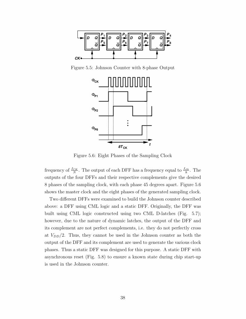
CK
D Q
Q Q Q Q
D Q D Q D Q1P P P P2 3 4
P P P P5 6 7 8
Figure 5.5: Johnson Counter with 8-phase Output
Φ
Φ
Φ
tCK
P1
P2
P8
ΦCK
8T
Figure 5.6: Eight Phases of the Sampling Clock
frequency of fCKN
. The output of each DFF has a frequency equal to fclk8
. The
outputs of the four DFFs and their respective complements give the desired
8 phases of the sampling clock, with each phase 45 degrees apart. Figure 5.6
shows the master clock and the eight phases of the generated sampling clock.
Two different DFFs were examined to build the Johnson counter described
above: a DFF using CML logic and a static DFF. Originally, the DFF was
built using CML logic constructed using two CML D-latches (Fig. 5.7);
however, due to the nature of dynamic latches, the output of the DFF and
its complement are not perfect complements, i.e. they do not perfectly cross
at VDD/2. Thus, they cannot be used in the Johnson counter as both the
output of the DFF and its complement are used to generate the various clock
phases. Thus a static DFF was designed for this purpose. A static DFF with
asynchronous reset (Fig. 5.8) to ensure a known state during chip start-up
is used in the Johnson counter.
38

M 3 M 4
M2M 1 M
5 M 6
CKCK
DD
Figure 5.7: Current Mode Logic based D-latch
φ
RST
φ
φ
φ
D
φ
φ
RST
Q
QRST
φ
φ
Figure 5.8: D Flip-flop with Asynchronous Reset
5.2 4-bit SAR sub-ADC
5.2.1 SAR sub-ADC Clocking Scheme
Several different clocks are used to ensure proper timing and functioning of
the various blocks comprising the SAR ADC. This section explains the role
of the different clocks used within one SAR sub-ADC. The operation of the
sub-ADC can be broken down into two main phases: the sampling phase and
the bit cycling phase. During the sampling phase the input is sampled onto
the capacitors of the SAR sampling network CDAC. This input voltage is
then quantized to the right value during the bit cycling phase. Five main
clocks shown in Fig. 5.9 are used in the SAR ADC:
• Sampling Clock, ΦPS: The input is sampled onto the capacitors of
the sampling network when the sampling clock is HIGH. The sampling
clock is generated by delaying the Early Sampling Clock.
• Early Sampling Clock, ΦPSe: The early sampling clock is an early
39

ΦCK
tCK8T
ΦPS
ΦPSe
Φ
Φ
BC
RS
ΦRST
Figure 5.9: Clocks Used in the SAR sub-ADC
version of the sampling clock. It is used to set the input node of the
comparator to virtual ground slightly prior to the sampling phase. This
is done to ensure that no charge is pulled out of the sampling network
through charge sharing when the switches connected to the virtual
ground node are closed. The early clock facilitates bottom-plate sam-
pling resulting in mitigation of input-dependent charge injection. The
early sampling clock is the clock generated by the Johnson counter.
• Bit Cycling Clock, ΦBC: The bit cycling clock is generated by gating
the complement of the sampling clock with the master clock. Thus bit
cycling clock is low for half the clock period while it produces pulses
at the master clock frequency during the other half. The positive edge
of the bit cycling clock is used to force a bit value onto the sampling
network while the negative edge of the clock is used to trigger the
comparator and latch the right logic value onto the selected bit. The
comparator block and the SAR Logic block operate on the complement
of the bit cycling clock.
• SAR Logic Reset, ΦRST : This signal is used to reset the outputs of
the D Flip-flops used in the SAR logic block to the right values prior
40
to the bit cycling phase. The SAR logic reset clock goes high half-way
through the sampling phase. This is done to ensure that the flip-flops
have enough time to reset as well as to make sure that the last bit
resolved by the SAR logic block has enough time to settle down. This
signal is generated by gating the sampling clock with a phase-shifted
sampling clock already generated by the Johnson counter. A phase
shift of 180 degree was chosen between the two clocks.
• Re-sampling Clock, ΦRS: The re-sampling clock is used to sample
the settled output of the SAR ADC at the right instant. A phase-
shifted version of the sampling clock is used as the re-sampling clock.
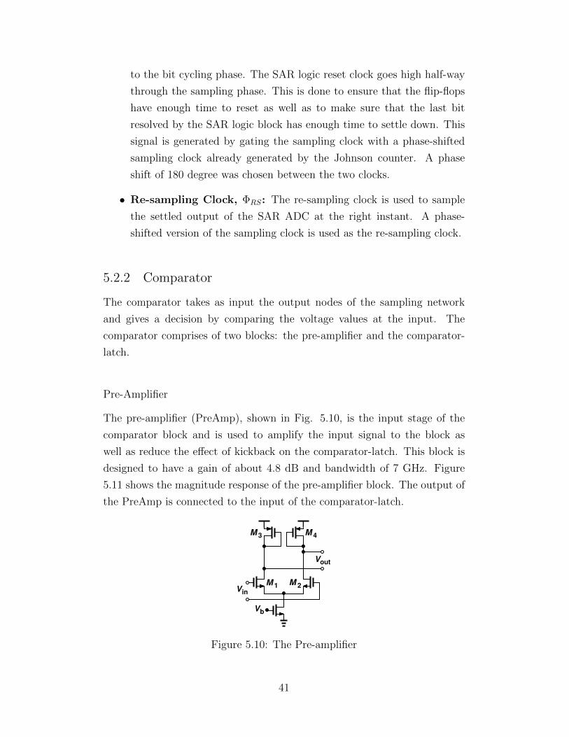
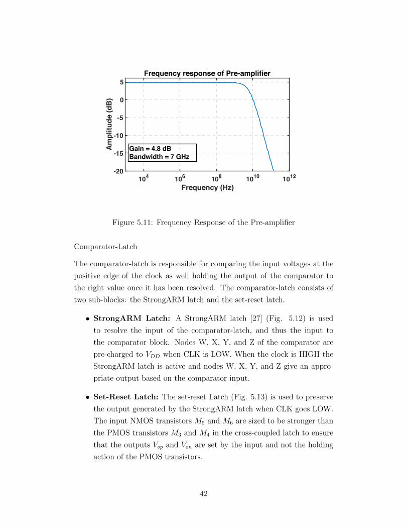
5.2.2 Comparator
The comparator takes as input the output nodes of the sampling network
and gives a decision by comparing the voltage values at the input. The
comparator comprises of two blocks: the pre-amplifier and the comparator-
latch.
Pre-Amplifier
The pre-amplifier (PreAmp), shown in Fig. 5.10, is the input stage of the
comparator block and is used to amplify the input signal to the block as
well as reduce the effect of kickback on the comparator-latch. This block is
designed to have a gain of about 4.8 dB and bandwidth of 7 GHz. Figure
5.11 shows the magnitude response of the pre-amplifier block. The output of
the PreAmp is connected to the input of the comparator-latch.
outV
Vb
M 2
M 3 M 4
M 1inV
Figure 5.10: The Pre-amplifier
41
104 106 108 1010 1012
Frequency (Hz)
-20
-15
-10
-5
0
5
Am
plitu
de (d
B)
Frequency response of Pre-amplifier
Gain = 4.8 dBBandwidth = 7 GHz
Figure 5.11: Frequency Response of the Pre-amplifier
Comparator-Latch
The comparator-latch is responsible for comparing the input voltages at the
positive edge of the clock as well holding the output of the comparator to
the right value once it has been resolved. The comparator-latch consists of
two sub-blocks: the StrongARM latch and the set-reset latch.
• StrongARM Latch: A StrongARM latch [27] (Fig. 5.12) is used
to resolve the input of the comparator-latch, and thus the input to
the comparator block. Nodes W, X, Y, and Z of the comparator are
pre-charged to VDD when CLK is LOW. When the clock is HIGH the
StrongARM latch is active and nodes W, X, Y, and Z give an appro-
priate output based on the comparator input.
• Set-Reset Latch: The set-reset Latch (Fig. 5.13) is used to preserve
the output generated by the StrongARM latch when CLK goes LOW.
The input NMOS transistors M5 and M6 are sized to be stronger than
the PMOS transistors M3 and M4 in the cross-coupled latch to ensure
that the outputs Vop and Von are set by the input and not the holding
action of the PMOS transistors.
42

M 2
M M
M 1
MM
M
M M
M
M
CLK
CLKCLK3 4
5 6
7 8
9 M 10
12
13Von
Vinp Vinn
M
M
14
15Vop
W X
Y Z
Figure 5.12: The StrongARM Latch
M 3 M 4
MMM M
VopVon
V Vinpinn1 25 6
Figure 5.13: The Set-Reset Latch
5.2.3 Sampling Network
The SAR sampling network is the primary interface between the external
input voltage and the SAR ADC. The sampling network consists of a binary
weighted capacitive DAC as shown in Fig. 5.14, which depicts a single-ended
implementation of the differential sampling network (Figures B.6 and B.7)
used in the SAR ADC. The switches S1, S2, S3, S4 and S5 are controlled by
the sampling clock and are connected to VIN during the sampling phase
while switch S6 controlled by the early sampling clock is connected to virtual
ground. During the bit cycling phase, switches S1, S2, S3, S4 and S5 are
controlled by a signal generated by gating the bit-cycling clock with the bits
outputted by the SAR logic block. The output of the sampling network is
connected to the input of the comparator block.
The switches S1, S2, S3, S4, S5 and S6 are realized using PMOS transistors
due to the high common-mode voltage used in the SAR ADC. The unit
capacitor C is chosen as 10 fF. The PMOS switches S1 and S2 connected
to the unit capacitors are chosen to be of size 1 µm. The switch sizes are
scaled by the same amount as the capacitor value ensuring that the RC time
constant of each branch remains the same.
43

C 8C4C2CC
inV
Vx
Vcomp
S
S 1 S S S S2 3 4 5
6
RV0b RVb RVb RVb RVb1 2 3 4
Figure 5.14: Single-ended 4-bit SAR Sampling Network Implementation
5.2.4 SAR Logic Block
The SAR logic block is responsible for implementing the bit-cycling logic that
is characteristic of SAR ADCs. This block ensures that the binary number
formed by the 4 bits (b3b2b1b0) is set to the right value during the sampling
as well as the bit-cycling phase of the SAR ADC.
Figure 5.15 shows the SAR logic block for a 2-bit SAR ADC and the timing
diagram of its signals. It consists of 2 chains of 3 DFFs. The top chain of
DFFs, DFF1-DFF2, are clocked by the complement of the bit-cycling clock
(ΦBC), labeled as ΦCK on Fig. 5.15. The outputs Q1, Q2 and Q3 are used
to SET the outputs of the bottom chain DFFs to 1 during the bit-cycling
phase. The bottom chain of flip-flops, DFF4-DFF6, are each clocked by it
successive DFF. During the sampling phase, the outputs Q2, Q3, B0 and X
are reset to 0 using the SAR logic reset signal (ΦRST ) while the outputs Q1
and B1 are set to 1. During the bit-cycling phase, at the positive edge of the
clock ΦCK , Q2 goes to 1, setting B0 to 1, this clocks DFF4 and causes B1
to latch to the comparator value. The output B0 is similarly latched to the
comparator value at the next clock edge.
The SAR sub-ADC is designed using synchronous SAR logic as shown in
Fig. 5.16. The 4-bit SAR logic block consists of 2 chains of 5 DFFs each. In
order to ensure that the comparator output in our sub-ADC has sufficient
time to settle, the SAR logic block is clocked using a delayed version of the
clock that triggers the comparator. The SAR logic block plays a critical
role in determining the maximum speed at which a single-channel SAR ADC
can operate. The DFFs used in the 4-bit SAR logic block (Fig. 5.16) are
optimized to reduce the delays along the critical path of the SAR logic block.
The set-to-Q and clock-to-Q delays of the set-reset D flip-flops (DFFSR) used
in the bottom chain of the SAR logic block contribute to the delay of this
44

D Q
Q
S
R
D Q
Q
SD Q
Q
S
R
D Q
Q
SD Q
QR
D Q
QR
CK
RST
1Q
B
Q3Q2
RST
1 B0 X
t
ΦRST
ΦQ3
ΦBC
ΦCK
ΦQ1
ΦQ2
Φ
Φ
Φ
B1
B0
X
COMP
COMP
COMP
1 2 3
4 5 6
Figure 5.15: 2-bit SAR Logic Block and relevant Timing Sequence
block. The DFFSR is especially designed to ensure that the set-to-Q delay of
the flip-flop is as small as possible as it is along the critical path. Figure 5.17
shows a conventional DFFSR. As seen in Fig. 5.18, the signal passes through
only one gate when the set signal is HIGH for the custom DFFSR while it
passes through 4 gates in the case of a conventional DFFSR. This ensures
that the output is set to HIGH as soon as possible once the set signal goes
HIGH. Thus, the overall delay of the SAR logic block is minimized. Chapter
6 presents a critical path analysis of the overall SAR sub-ADC as well as the
SAR logic block. Figures B.12, B.13 and B.14 in Appendix B.1 show the
circuit schematics of the three types of DFFs used in the SAR logic block.
45

D Q
Q
S
R
D Q
Q
SD Q
Q
S
R
D Q
Q
S
R
D Q
Q
S
R
D Q
Q
SD Q
QR
D Q
QR
D Q
QR
D Q
QR
COMP
CK
RST
1
1Q
B B B B2 03
Q5Q4Q3Q2
RST
Figure 5.16: 4-bit SAR Logic Block
φ
φ
RST
φ
φ
D
φ
φQ
RST
φ
φ
SET
SET
Figure 5.17: Custom Set-Reset D Flip-flop
46

φ
φ
φ
φ
φ
SET
SET
RST
RST
SET
φ
φ
φ
Q
QD
RST
RST
Figure 5.18: Custom Set-Reset D Flip-flop
47

5.3 Simulation Results
This section gives the simulation results of the single channel 4-bit sub-ADC
as well as the performance of the overall 8-channel time-interleaved ADC.
5.3.1 Single-Channel Simulation Results
Figure B.2 in Appendix B.1 shows the top-level test-bench schematic of the
4-bit SAR sub-ADC implemented. The 4-bit sub-ADC was tested using the
625 MHz sampling clock frequency. The bits generated from the SAR logic
block were sampled using the re-sampling clock and stored in a D flip-flop.
The final sampled binary code (b3b2b1b0) was then converted to decimal to
give the quantized output waveform. A 128-point FFT on the quantized
output gives us an SNR of 23.84 dB for a low-frequency input and an SNR
of 24.32 for a high-frequency (2.49 GHz) input signal. Figures 5.19 and 5.20
show the spectrum of the output for two cases. Since the sampling frequency
for the single channel case does not satisfy the Nyquist theorem with this
input signal, the output aliases to a lower frequency and thus apppear to be
near the DC value.
0 50 100 150 200 250 300Frequency (MHz)
-40
-20
0
20
Am
plitu
de (d
B)
Low-frequency Spectrum of 4-bit SAR sub-ADCSNR = 23.84 dB
Figure 5.19: Output Spectrum of the 4-bit SAR Sub-ADC Using aLow-Frequency Input Signal
48

0 50 100 150 200 250 300Frequency (MHz)
-40
-20
0
20
Am
plitu
de (d
B)
High-frequency Spectrum of 4-bit SAR sub-ADCSNR = 24.32 dB
Figure 5.20: Output Spectrum of the 4-bit SAR Sub-ADC Using aHigh-Frequency Input Signal
5.3.2 Time-interleaved ADC Simulation Results
The single-channel 4-bit SAR ADC design is used as a sub-ADC in an 8-
channel time-interleaved ADC. Eight copies of the 4-bit SAR sub-ADC each
clocked at 625 MHz are operated in parallel on different phases of the sam-
pling clock each 45 degrees apart. This causes the different sub-ADCs to
operate on different input samples. The output from each of the sub-ADCs
is then time-interleaved, creating an ADC operating at 8 times the frequency
of each single-channel sub-ADC, i.e. at 5 GHz. Figure B.15 in Appendix B.1
shows the top-level test-bench schematic of the 8-channel time-interleaved
4-bit SAR sub-ADC implemented.
The ADC consumes a power of 42.6 mW, effective number of bits (ENOB)
of 3.74 and figure-of-merit (FoM) of 638 fJ/conversion-step for an input close
to Nyquist frequency. Figures 5.21 and 5.22 show the output spectra of the
ADC with a low-frequency and high-frequency input respectively. The ADC
achieves an SNR of 23.7 dB for a low-frequency input signal and a SNR of
24.30 dB for a high-frequency input.
49

0 500 1000 1500 2000 2500Frequency (MHz)
-60
-40
-20
0A
mpl
itude
(dB
) SNR = 23.7 dBSFDR = 30.6 dB
Figure 5.21: Low-Frequency Output Spectrum of 8-channelTime-interleaved SAR ADC
0 500 1000 1500 2000 2500 3000Frequency (MHz)
-60
-40
-20
0
Am
plitu
de (d
B) SNR = 24.30 dB
SFDR = 34.1 dB
Figure 5.22: High-Frequency Output Spectrum of 8-channelTime-interleaved SAR ADC
50
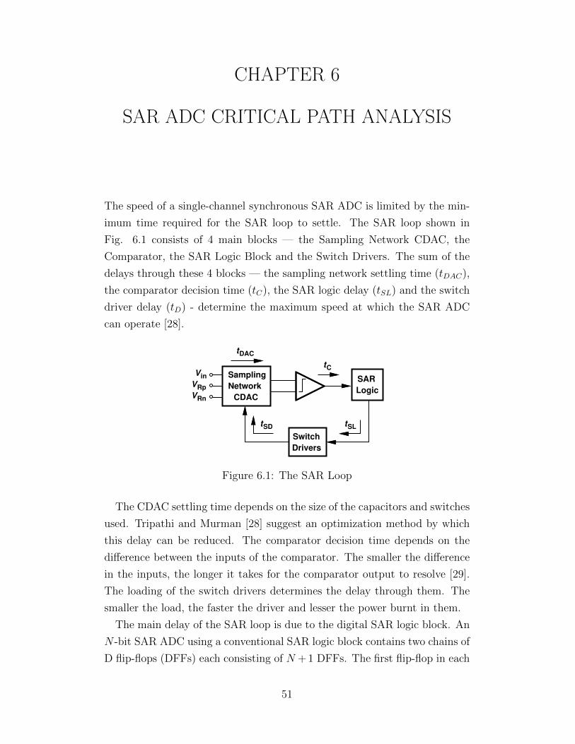
CHAPTER 6
SAR ADC CRITICAL PATH ANALYSIS
The speed of a single-channel synchronous SAR ADC is limited by the min-
imum time required for the SAR loop to settle. The SAR loop shown in
Fig. 6.1 consists of 4 main blocks — the Sampling Network CDAC, the
Comparator, the SAR Logic Block and the Switch Drivers. The sum of the
delays through these 4 blocks — the sampling network settling time (tDAC),
the comparator decision time (tC), the SAR logic delay (tSL) and the switch
driver delay (tD) - determine the maximum speed at which the SAR ADC
can operate [28].
Sampling
Network
CDAC
SAR
Logic
Switch
Drivers
inV
VRp
VRn
DAC
C
SD
t
t
SLtt
Figure 6.1: The SAR Loop
The CDAC settling time depends on the size of the capacitors and switches
used. Tripathi and Murman [28] suggest an optimization method by which
this delay can be reduced. The comparator decision time depends on the
difference between the inputs of the comparator. The smaller the difference
in the inputs, the longer it takes for the comparator output to resolve [29].
The loading of the switch drivers determines the delay through them. The
smaller the load, the faster the driver and lesser the power burnt in them.
The main delay of the SAR loop is due to the digital SAR logic block. An
N -bit SAR ADC using a conventional SAR logic block contains two chains of
D flip-flops (DFFs) each consisting of N + 1 DFFs. The first flip-flop in each
51

COMP
D Q
Q
S
R
D Q
Q
S D Q
Q
S
R
D Q
Q
S D Q
QR
D Q
QR
CK
RST
1Q
B
Q3Q2
RST
1 B0 X
1 2 3
4 5 6
Critical path
Figure 6.2: A 2-bit SAR Logic Block
chain is a DFF with an asynchronous set (DFFS). The top chain consists of
N DFFs with an asynchronous reset (DFFR) while the bottom chain consists
of N DFFs with asynchronous set-reset (DFFSR).
Figure 6.2 shows the SAR logic block for a 2-bit SAR ADC and Fig. 6.3
shows its timing diagram. The outputs Q1, Q2 and Q3 serve as pointers to
the bit being resolved and SET the outputs of the bottom chain DFFs to
HIGH when clocked by ΦCK . The bottom chain of flip-flops with outputs
B1 and B0 are each clocked by it successive DFF. At the positive edge of
the clock ΦCK , Q2 goes HIGH, setting B0 HIGH, this clocks the DFF4 and
causes B1 to latch to the comparator value.
The latched value of B1 during the bit-cycling phase is then applied to the
sampling network at the next positive edge of the bit cycling-clock, ΦBC . B1
thus needs to latch to the right value within half a clock period (TCK2
) after
the occurrence of the rising edge of ΦCK . Thus, the path from the input of
DFF2 to DFF5 to the output of DFF4 forms the critical path of the SAR
logic block. Since the comparator is clocked at the rising edge of ΦCK as
well, it is important that the comparator output settles to the right value
before B1 is clocked and latched. Thus, for proper functioning of the SAR
logic block it is important that the inequality given by (6.1) is satisfied.
tCQ2+ tSQ5
> tC + tSU4(6.1)
52

ΦCK
COMP
ΦQ2Ct
tCQ2
t
ΦB0
ΦB1
tSQ5
COMP
CK T
tCQ4
Figure 6.3: Timing Diagram of 2-bit SAR Logic Block with Critical PathDelays
where, tCQ2: clock-to-Q delay of DFF2
tSQ5: set-to-Q delay of DFF5
tC : comparator decision time
tSU4 : set-up time of DFF4
The speed at which the SAR logic block can operate is thus limited by the
speed of the comparator and the DFFs.
tC + tCQ2+ tSQ5
+ tCQ4<TCK
2(6.2)
The maximum bit-cycling frequency, fCKmax1 is thus given by equation 6.3.
∴ fCKmax <1
2(tC + tCQ2+ tSQ5
+ tCQ4)
(6.3)
where, TCK : time period of the bit-cycling clock
1The maximum bit-cycling frequency is the maximum frequency at which the bits in asingle-channel SAR ADC can be resolved.
53

Table 6.1: Critical Path Delays
Custom DFFDelay
ConventionalDFF Delay
% improve-ment
tC w/ 800µVoffset
98.35 ps 98.35 ps 0%
tC w/ 1LSBoffset
84.7 ps 84.7 ps 0%
tCQ2 21.69 ps 34 ps 36.2%tSQ5 20.42 ps 50 ps 59.2%tCQ4 30 ps 42 ps 28.6%Ttotal 156.81 ps 210.7 ps 25.6%
Table 6.1 shows the values of the delays in the critical path and compares
the delays of the custom DFFs used in the SAR sub-ADC design with that
of a conventional DFF.
54

CHAPTER 7
SAR QUANTIZER PERFORMANCEENHANCEMENT
The performance of the SAR quantizer can be further enhanced by increasing
the number of ADC bits. The 4-bit SAR ADC design described in chapter
5 is thus extended to form an 8-bit SAR ADC. As the number of bits in an
ADC increases, the sizes of the sampling network capacitors and power con-
sumed by buffers to drive large capacitances increase accordingly. Therefore,
various design changes need to be made to ensure high-speed performance at
low power for the increased ADC resolution. In this chapter, the design of a
16-channel time-interleaved 5 GS/s 8-bit SAR ADC using synchronous SAR
logic and several speed enhancement techniques has been described. Each
sub-ADC is designed to operate at 1/16th the clock frequency, i.e. at a sam-
pling frequency of 312.5 MHz. Similar to the 4-bit SAR ADC, the operation
of the 8-bit SAR ADC is split into two phases - the sampling phase and the
bit-cycling phase. The bit-cycling phase, however, requires 8 rising edges
to process the 8-bits compared to the four edges used in the 4-bit case and
hence the clock frequency is divided by 1/16th. The bit-cycling clock thus
consists of 8 pulses during the bit-cycling phase. The clocking scheme of the
8-bit SAR sub-ADC is the same as the 4-bit SAR in terms of the relevant
clocks used in the SAR sub-ADC. The relevant clocks are also generated in
same manner as they are in the 4-bit case. Similarly, the same comparator
block is used in both the ADCs. The significant change in design for the
8-bit sub-ADC is made in the sampling network and the multi-phase clock
generator and has been described in this chapter.
7.1 Multi-phase Clock Generator
The 8-bit SAR ADC requires 16-channel time-interleaving; thus, 16 phases of
the sampling clock need to be generated. Similar to the 4-bit ADC, the multi-
55

phase clock generator for the 8-bit sub-ADC consists of a CML to CMOS
converter followed by a Johnson counter. The 16-phases of the sampling
clock are generated using a 16-phase Johnson counter. The 16-phase Johnson
counter (Fig. 7.1) was built using 8 D flip-flops. The outputs of the 8 DFFs
and their respective complements give the desired 16 phases of the sampling
clock, with each phase 22.5 degrees apart. Figure 7.2 shows the master clock
and the 16 phases of the sampling clock generated.
CK
D Q
Q Q Q Q
D Q D Q D Q
P P P P
D Q
Q Q Q Q
D Q D Q D Q1P P P2 3 P 4 5 6 7 8
P P P PP P P9 10 11 P 12 13 14 15 16
Figure 7.1: 16-phase Johnson Counter
ΦCK
Φ
Φ
Φ
t
P1
P2
CK
P16
16T
Figure 7.2: 16 Phases of the Sampling Clock
7.2 8-bit SAR sub-ADC
7.2.1 Sampling Network
Several sampling network topologies were explored before designing the sam-
pling network for the 8-bit SAR ADC. Several sampling network topologies
have been used in SAR ADCs in literature, such as binary weighted CDAC
56

[28], split-capacitive array DAC with unit bridge capacitor [30] and C-2C
ladder [31]. In order to reduce the capacitive loading of the sampling net-
work, the split-array topology with a unit bridge capacitor was used to design
the 8-bit sampling network. The reduced capacitor size of the sampling net-
work reduces the loading of the input buffer as well as the reference buffers,
thereby reducing the power consumed by them [32].
Binary weighted CDACs are good for low-resolution SAR ADCs (< 6
bits) but as the number of bits increases the size of the capacitor array, and
thus the area of sampling network, increases exponentially. An N -bit binary
weighted SAR requires 2N unit capacitors (C). The size of the sampling net-
work capacitance can be significantly reduced by using the split-capacitor
SAR. An N -bit SAR using this structure only requires 2N2
+1 − 1 unit ca-
pacitors. Thus, the split CDAC for the 8-bit SAR sub-ADC uses 31 unit-
capacitors (C) with an input loading of 16C compared to a binary-weighted
CDAC that would use 256 unit capacitors with an input loading of 256C.
Therefore, the input capacitance and area occupied by the sampling network
is significantly reduced compared to the binary-weighted capacitor topology.
A split-array with a unit bridge capacitor rather than a fractional bridge
capacitor is used as a fractional bridge capacitor causes poor matching with
the other capacitors [16].
Although the C-2C sampling network occupies the least area as it only
requires 3 ∗ N capacitors [31] for a N-bit ADC, it suffers significantly due
to top and bottom-plate parasitics compared to the split-capacitor SAR.
The split-capacitor SAR also suffers from top and bottom-plate parasitics
of the bridge capacitor [30] as well as a 1LSB gain error [16]; however, as
seen from the simulation results in section 7.3 this does not cause significant
degradation in the SNR for a medium resolution ADC.
The 8-bit sampling network CDAC uses two 4-bit capacitor arrays to serve
as the LSB and MSB arrays. The same capacitor array as the one designed for
the 4-bit SAR is used after removing the dummy capacitors that were present
in the 4-bit SAR array. Figure 7.3 shows a single-ended implementation of
the differential sampling network CDAC used in the 8 bit SAR sub-ADC.
The value of bridge capacitor Cb is equal to the unite capacitance C. The
unit capacitance C, is designed to be as small as permitted by the thermal
noise requirement, and is chosen to be of 10 fF. The switches S1-S9 are sized
such that the RC time constant of each switch-capacitor pair is the same,
57

Cb
2CC
S S1 2
inV
RVb RVb0 1
Vcomp
S2CC
S S
Vx
Rb RVb
S S
RVb RVb
4C 8C
S S3 4
RVb2 RVb3
4C 8C
5 6 7 8
9
V4 5 6 7
Figure 7.3: Single-ended 8-bit SAR Sampling Network Implementation
i.e. S1 × C = S2 × 2C. The sampling network uses all PMOS switches with
the minimum sized switch, S1 having a width of 1µm.
7.2.2 8-Bit SAR Logic Block
The 4-bit SAR logic block designed for the 4-bit SAR ADC is extended to
build the SAR logic block for the 8-bit SAR. Figure 7.4 shows the 8-bit SAR
logic block used in the 8-bit SAR ADC. The 8-bit implementation of the
SAR logic block consists of two chains of D flip-flops (DFF) consisting of 9
DFFs each. The signals B7B6B5B4B3B2B1B0 gives the 8-bit output of the
SAR ADC.
D Q
Q
S
R
D Q
Q
S
D Q
Q
S D Q
QR
COMP
CK
RST
1Q
B B
Q2
7 6
RST
D Q
Q
S
R
D Q
Q
S
R
D Q
QR
D Q
QR
B0
QQ 98
Figure 7.4: 8-bit SAR Logic Block
58

7.3 Simulation Results
The ADC is designed in 65 nm CMOS and uses a supply voltage of 1.2 V. A
common-mode voltage of 1.1 V is used and positive and negative reference
voltages of 1.3 V and 0.9 V are used respectively. This section gives the simu-
lation results of the single channel 8-bit sub-ADC as well as the performance
of the overall 16-channel time-interleaved ADC.
7.3.1 Single-Channel Simulation Results
Figure B.16 in Appendix B.3 shows the top-level test-bench schematic of the
8-bit SAR sub-ADC implemented. The 8-bit sub-ADC was tested using the
312.5 MHz sampling clock frequency. The bits generated from the SAR logic
block are sampled using the re-sampling clock and stored in a D flip-flop.
The final sampled binary code (b7b6b5b4b3b2b1b0) is then converted to decimal
to give the quantized output waveform. The 8-bit SAR sub-ADC was tested
using both an ideal sampling network consisting of ideal switches as well as
the real sampling network consisting of the PMOS switches.
The SAR ADC consisting of the ideal sampling network gives us an SNR of
45.67 dB which is close to the expected value of 50 dB for an 8-bit ADC. The
SAR ADC consisting of the real sampling network gives us an SNR of 45.09
dB for a low-frequency input signal which is a little lower than expected.
Figure 7.5 shows the frequency spectrum of the output for the two sampling
network cases. Figure 7.6 shows the output spectrum for a high-frequency
input signal of 2.49 GHz. Since the sampling frequency for the single channel
case does not satisfy the Nyquist criterion with this input signal, the output
aliases to a lower frequency and thus apppears to be near the DC value. The
SNR in this case is 44.17 dB.
This degradation in SNR can be attributed to two factors: the race con-
dition in the SAR logic block and the parasitic effects at the capacitor input
node. On further examining the circuit, it is seen that there is a race condi-
tion between when the right comparator output is latched onto the output
bits of the SAR logic block and when the next bit is applied to the sampling
network during the bit-cycling phase. A frequency of 5 GHz does not provide
the output of the SAR logic block sufficient time to settle to the right value
within half a clock cycle. The effects of this race can be mitigated by op-
59

0 50 100 150Frequency (MHz)
-40
-20
0
20
40
Am
plitu
de (d
B)
Output Spectrum of 8-bit SAR sub-ADCSNRideal = 45.67 dBSNRreal = 45.09 dB
Figure 7.5: Low-Frequency Output Spectrum of the 8-Bit SAR sub-ADCUsing Ideal and Real Switches
erating the SAR ADC at a lower frequency. This issue can also be resolved
by reducing the duration of the sampling phase and increasing the time for
the bit-cycling phase. This would provide a longer time for bit-cycling to
occur and thus give the SAR logic outputs a longer time to settle. The para-
sitic capacitance resulting from the top and bottom plate capacitance of the
bridge capacitor introduces a mismatch between the LSB and MSB array.
This in turn contributes to the degradation in the SAR ADC’s performance.
Capacitors can be connected across the bridge capacitor and in parallel with
the LSB array to combat the effect of the parasitic capacitance introduced
at the comparator input [16].
60

0 50 100 150Frequency (MHz)
-40
-20
0
20
40
Am
plitu
de (d
B)
High-frequency Spectrum of 8-bit SAR sub-ADCSNR = 44.17 dB
Figure 7.6: Output Spectrum of the 8-bit SAR Sub-ADC Using aHigh-Frequency Input Signal
61

Table 7.1: Power Breakdown
Power [mW] PercentageComparator 29.70 32.00%
Clock 56.40 60.80%SAR Logic 6.36 6.85%Reference 0.36 0.38%
Total 92.8 100%
7.3.2 Time-interleaved ADC Simulation Results
The single-channel 8-bit SAR ADC design is used as a sub-ADC in a 16-
channel time-interleaved ADC. Sixteen copies of the 8-bit SAR sub-ADC
each clocked at 312.5 MHz are operated in parallel on different phases of
the sampling clock each 22.5 degrees apart. This causes the different sub-
ADCs to operate on different input samples. The output from each of the
sub-ADCs is then time-interleaved, creating an ADC operating at 16 times
the frequency of each single-channel sub-ADC, i.e. at 5 GHz. Figure B.22
in Appendix B.3 shows the top-level test-bench schematic of the 16-channel
time-interleaved 8-bit SAR sub-ADC implemented.
The ADC consumes a power of 92.8 mW at 5 GS/s when the input is at
Nyquist frequency. Table 7.1 shows a breakdown of the power consumed by
the different circuit components.
Figures 7.7 and 7.8 show the output spectra of the ADC with low-frequency
and high-frequency inputs respectively. The degradation in SNR for a high-
frequency input is due to the timing mismatch in time-interleaving.
An input close to Nyquist frequency gives SNR of 41.5 dB and a SFDR of
46.3 dB. The effective number of bits (ENOB) at Nyquist of the ADC given
by (7.1) is 6.60 and the Walden figure-of-merit (FoM) given by (7.2) is 191
fJ/conversion-step. Table 7.2 summarizes the performance of the ADC and
compares it with state-of-the-art ADCs [33].
ENOB =SNRdB − 1.76
6.02(7.1)
FoM =Power
2ENOB × fS[J/conv-step] (7.2)
62

0 500 1000 1500 2000 2500Frequency (MHz)
-80
-60
-40
-20
0A
mpl
itude
(dB
) SNR = 45.1 dBSFDR = 56.3 dB
Figure 7.7: Low-Frequency Output Spectrum of 16-channelTime-interleaved SAR ADC
0 500 1000 1500 2000 2500 3000Frequency (MHz)
-80
-60
-40
-20
0
Am
plitu
de (d
B) SNR = 41.5 dB
SFDR = 46.3 dB
Figure 7.8: High-Frequency Output Spectrum of 16-channelTime-interleaved SAR ADC
63

Table 7.2: Performance Comparison
Thiswork
[34] [35] [36] [31] [37]
Architecture Ti-SAR Ti-SAR Ti-SARFoldingFlash
Ti-SARTi-Pipeline
Technology[nm]
65 40 45 40 65 350
Resolution[bits]
8b 8b 6b 7b 7b 8b
SamplingRate [GS/s]
5 2 5 2.2 2.5 4
SupplyVoltage (V)
1.2 - 1 1.1 1.1 3.3
Power[mW]
92.8 54.2 50.0 27.4 50.0 4600.0
SNDR [dB] 41.5 39.4 30.8 37.4 34 39.1SFDR [dB] 46.3 55.13 43 44 45 -ENOB 6.60 6.25 4.8 5.9 5.4 6.20FoM[fJ/conv-step]
191 355 39 205.7 555.1 15642
64

CHAPTER 8
CONCLUSION
In this thesis high-speed successive approximation register based analog-to-
digital converters are implemented in 65 nm CMOS with the motivation to
use them in a high-speed delta-sigma modulator. An 8-channel 4-bit time-
interleaved SAR analog-to-digital converter operating at a sampling rate of
5GS/s is implemented using synchronous successive approximation logic. A
single channel in the 4-bit ADC achieves a signal-to-noise ratio (SNR) of
23.84 dB for a low-frequency input and SNR of 24.32 dB for an input signal
close to Nyquist. The 8-channel time-interleaved 4-bit SAR ADC consumes
power of 42.6 mW, achieves ENOB of 3.74 and FoM of 638 fJ/conversion-
step. The time-interleaved ADC achieves SNR of 23.7 dB for a low-frequency
input and SNR of 24.3 dB for a high-frequency input signal.
The implementation of the 4-bit SAR ADC is extended to 8-bit to im-
plement an 8-bit SAR ADC operating at a sampling rate of 5GS/s using
16-channel time-interleaving. The single-channel sub-ADCs achieve SNR of
45.09 dB and 44.17 dB for low- and high-frequency input signals respectively.
The 16-channel time-interleaved 8-bit SAR ADC achieves ENOB of 6.6 bits,
figure-of-merit of 191 fJ/conversion-step and power consumption of 92.8 mW.
The 8-bit time-interleaved ADC achieves SNR of 41.5 dB and SFDR of 46.3
dB for input signals close to Nyquist.
The high-speed operation of the SAR ADCs is achieved by optimizing
the delays in the SAR loop. A critical path analysis for the delays in a
SAR ADC using synchronous SAR logic and an analysis of the maximum
achievable frequency of operation has also been presented.
65

REFERENCES
[1] R. Schreier and G. C. Temes, Understanding Delta Sigma Data Con-verters. IEEE Press, 2005.
[2] M. Bolatkale, L. J. Breems, R. Rutten, and K. A. A. Makinwa, “A 4GHz continuous-time delta-sigma ADC with 70 dB DR and - 74 dBFSTHD in 125 MHz BW,” IEEE Journal of Solid-State Circuits, vol. 46,no. 12, pp. 2857–2868, Dec 2011.
[3] Y. Dong, J. Zhao, W. W. Yang, T. Caldwell, H. Shibata, Z. Li,R. Schreier, Q. Meng, J. B. Silva, D. Paterson, and J. C. Gealow,“A 72 dB-DR 465 MHz-BW continuous-time 1-2 MASH ADC in 28nm CMOS,” IEEE Journal of Solid-State Circuits, vol. 51, no. 12, pp.2917–2927, Dec 2016.
[4] T. Caldwell, D. Alldred, R. Schreier, H. Shibata, and Y. Dong, “Ad-vances in high-speed continuous-time delta-sigma modulators,” in Pro-ceedings of the IEEE 2014 Custom Integrated Circuits Conference, Sept2014, pp. 1–8.
[5] L. Kull, T. Toifl, M. Schmatz, P. A. Francese, C. Menolfi, M. Brndli,M. Kossel, T. Morf, T. M. Andersen, and Y. Leblebici, “A 3.1 mW 8b 1.2GS/s single-channel asynchronous SAR ADC with alternate compara-tors for enhanced speed in 32 nm digital SOI CMOS,” IEEE Journal ofSolid-State Circuits, vol. 48, no. 12, pp. 3049–3058, Dec 2013.
[6] J. A. Fredenburg and M. P. Flynn, “A 90-MS/s 11-MHz-bandwidth62-dB SNDR noise-shaping SAR ADC,” IEEE Journal of Solid-StateCircuits, vol. 47, no. 12, pp. 2898–2904, Dec 2012.
[7] K. S. Kim, J. Kim, and S. H. Cho, “Nth-order multi-bit Delta-SigmaADC using SAR quantiser,” Electronics Letters, vol. 46, no. 19, pp.1315–1316, Sept 2010.
[8] P. P. Shingare and R. V. Shinde, “Analog to digital converter usingdelta sigma loop for the application portable ECG device,” in Interna-tional Conference on Recent Advances and Innovations in Engineering(ICRAIE-2014), May 2014, pp. 1–4.
66

[9] S. Pavan and N. Krishnapura, “Oversampling analog-to-digital con-verter design,” in 21st International Conference on VLSI Design (VL-SID 2008), Jan 2008, pp. 7–7.
[10] S. P. Lipshitz, R. A. Wannamaker, and J. Vanderkooy, “Quantizationand dither: A theoretical survey,” Journal of the Audio EngineeringSociety, vol. 40, no. 5, pp. 355–375, 1992.
[11] A. V. Oppenheim and R. Schafer, Digital Signal Processing. Prentice-Hall, 1975.
[12] D. A. Johns and K. Martin, Analog Integrated Circuit Design. JohnWiley & Sons, 2008.
[13] M. S. O. Alink, A. B. J. Kokkeler, E. A. M. Klumperink, K. C. Rovers,G. J. M. Smit, and B. Nauta, “Spurious-free dynamic range of a uni-form quantizer,” IEEE Transactions on Circuits and Systems II: ExpressBriefs, vol. 56, no. 6, pp. 434–438, June 2009.
[14] R. J. Van de Plassche, CMOS Integrated Analog-to-digital and Digital-to-analog Converters. Springer Science & Business Media, 2013, vol.742.
[15] B. Razavi, Principles of Data Conversion System Design. IEEE Press,1995.
[16] Y. Chen, X. Zhu, H. Tamura, M. Kibune, Y. Tomita, T. Hamada,M. Yoshioka, K. Ishikawa, T. Takayama, J. Ogawa, S. Tsukamoto, andT. Kuroda, “Split capacitor DAC mismatch calibration in successive ap-proximation adc,” in 2009 IEEE Custom Integrated Circuits Conference,Sept 2009, pp. 279–282.
[17] H. Inose and Y. Yasuda, “A unity bit coding method by negative feed-back,” Proceedings of the IEEE, vol. 51, no. 11, pp. 1524–1535, Nov1963.
[18] G. C. Temes, “Oversampling A/D and D/A converters,” in 9th EuropeanSignal Processing Conference (EUSIPCO 1998), Sept 1998, pp. 1–4.
[19] W. Kester, “ADC architectures iii: Sigma-delta ADC basics,” AnalogDevices, MT022, 2008.
[20] G. C. Temes and J. C. Candy, “A tutorial discussion of the oversamplingmethod for A/D and D/A conversion,” in IEEE International Sympo-sium on Circuits and Systems, May 1990, pp. 910–913 vol.2.
[21] B. A. Wooley, “Cascaded noise-shaping modulators for oversampled dataconversion,” in Proceedings of the IEEE 2003 Custom Integrated CircuitsConference, 2003., Sept 2003, pp. 113–114.
67

[22] B. Razavi, “Problem of timing mismatch in interleaved ADCs,” in Pro-ceedings of the IEEE 2012 Custom Integrated Circuits Conference, Sept2012, pp. 1–8.
[23] L. Wang, “Timing skew calibration for time interleaved analog to digitalconverters,” Ph.D. dissertation, University of Toronto, 2014.
[24] J. C. Chien and L. H. Lu, “Analysis and design of wideband injection-locked ring oscillators with multiple-input injection,” IEEE Journal ofSolid-State Circuits, vol. 42, no. 9, pp. 1906–1915, Sept 2007.
[25] X. Gao, E. A. M. Klumperink, and B. Nauta, “Advantages of shiftregisters over dlls for flexible low jitter multiphase clock generation,”IEEE Transactions on Circuits and Systems II: Express Briefs, vol. 55,no. 3, pp. 244–248, March 2008.
[26] J. op den Brouw, “An introduction to ring counters,” The Hague Uni-versity of Applied Sciences, Technical Report, 2015.
[27] B. Razavi, “The strongarm latch [a circuit for all seasons],” IEEE Solid-State Circuits Magazine, vol. 7, no. 2, pp. 12–17, Spring 2015.
[28] V. Tripathi and B. Murmann, “An 8-bit 450-MS/s single-bit/cycle SARADC in 65-nm CMOS,” in 2013 Proceedings of the ESSCIRC (ESS-CIRC), Sept 2013, pp. 117–120.
[29] S. W. M. Chen and R. W. Brodersen, “A 6-bit 600-MS/s 5.3-mW asyn-chronous ADC in 0.13- µm CMOS,” IEEE Journal of Solid-State Cir-cuits, vol. 41, no. 12, pp. 2669–2680, Dec 2006.
[30] A. Agnes, E. Bonizzoni, P. Malcovati, and F. Maloberti, “A 9.4-ENOB1v 3.8µW 100kS/s SAR ADC with time-domain comparator,” in 2008IEEE International Solid-State Circuits Conference - Digest of TechnicalPapers, Feb 2008, pp. 246–610.
[31] E. Alpman, H. Lakdawala, L. R. Carley, and K. Soumyanath, “A 1.1V50mW 2.5GS/s 7b time-interleaved C-2C SAR ADC in 45nm LP digitalCMOS,” in 2009 IEEE International Solid-State Circuits Conference -Digest of Technical Papers, Feb 2009, pp. 76–77,77a.
[32] S. K. Gupta, M. A. Inerfield, and J. Wang, “A 1-GS/s 11-bit ADCwith 55-dB SNDR, 250-mW power realized by a high bandwidth scal-able time-interleaved architecture,” IEEE Journal of Solid-State Cir-cuits, vol. 41, no. 12, pp. 2650–2657, Dec 2006.
[33] B. Murmann, “ADC performance survey 1997-2016.” [Online].Available: http://web.stanford.edu/ murmann/adcsurvey.html
68

[34] T. Miki, T. Ozeki, and J. i. Naka, “A 2GS/s 8b time-interleaved SARADC for millimeter-wave pulsed radar baseband SoC,” in 2016 IEEEAsian Solid-State Circuits Conference (A-SSCC), Nov 2016, pp. 5–8.
[35] C. H. Chan, Y. Zhu, S. W. Sin, U. Seng-Pan, and R. P. Martins,“A 5.5mW 6b 5GS/s 4×time-interleaved 3b/cycle SAR ADC in 65nmCMOS,” in 2015 IEEE International Solid-State Circuits Conference -(ISSCC) Digest of Technical Papers, Feb 2015, pp. 1–3.
[36] M. Miyahara, I. Mano, M. Nakayama, K. Okada, and A. Matsuzawa,“22.6 a 2.2GS/s 7b 27.4mW time-based folding-flash ADC with resis-tively averaged voltage-to-time amplifiers,” in 2014 IEEE InternationalSolid-State Circuits Conference Digest of Technical Papers (ISSCC), Feb2014, pp. 388–389.
[37] K. Poulton, R. Neff, A. Muto, W. Liu, A. Burstein, and M. Hes-hami, “A 4 GS/s 8b ADC in 0.35 µm CMOS,” in 2002 IEEE Interna-tional Solid-State Circuits Conference. Digest of Technical Papers (Cat.No.02CH37315), vol. 1, Feb 2002, pp. 166–457 vol.1.
69

APPENDIX A
SIMULINK MODELS
This appendix contains the Simulink models used to implement the MOD2
and MOD5 ADCs.
A.1 Second-order Delta-Sigma Modulator Simulink
Models
1
Out1
1
In1
8-level ADC
Subsystem
8-level ADC
Subsystem1
8-level ADC
Subsystem2
8-level ADC
Subsystem3
Add
2
Out2
Figure A.1: Simulink Model of 33-level Flash ADC
70

8-level DAC
Subsystem8
8-level DAC
Subsystem11
1
In1 1
Out1Add
8-level DAC
Subsystem2
8-level DAC
Subsystem1
Figure A.2: Simulink Model of 33-level DAC
71

APPENDIX B
CADENCE SCHEMATICS
This appendix contains Cadence schematics of the 4-bit SAR sub-ADC, the
8-channel TI 4-bit SAR ADC, the 8-bit SAR sub-ADC and the 16-channel
TI 8-bit SAR ADC.
B.1 4-Bit SAR sub-ADC Schematics
Figure B.1: CML D-Latch
72

Figure B.2: Top-level Test-bench Schematic for 4-bit SAR ADC
Figure B.3: 8 Phase Clock Generator
73

Figure B.4: Clocks for 4-Bit SAR
Figure B.5: 4-bit SAR ADC
74

Figure B.6: 4-bit Differential SAR Sampling Network
Figure B.7: Differential Half-circuit of 4-bit SAR Sampling Network
Figure B.8: The Comparator Block
75

Figure B.9: The Pre-amplifier
Figure B.10: The Comparator-latch
76

Figure B.11: 4-bit SAR Logic Block
Figure B.12: D Flip-flop with Asynchronous Reset
77

Figure B.13: D Flip-flop with Asynchronous Set
Figure B.14: D Flip-flop with Asynchronous Set-Reset
78
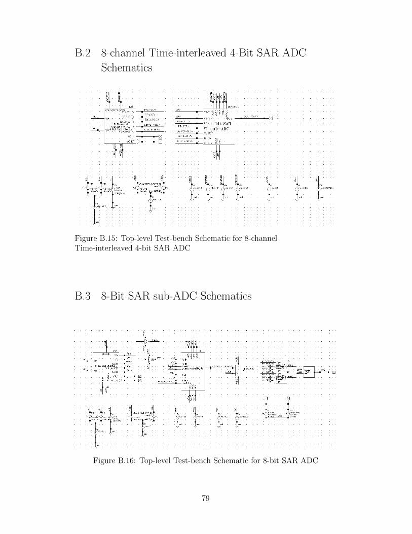
B.2 8-channel Time-interleaved 4-Bit SAR ADC
Schematics
Figure B.15: Top-level Test-bench Schematic for 8-channelTime-interleaved 4-bit SAR ADC
B.3 8-Bit SAR sub-ADC Schematics
Figure B.16: Top-level Test-bench Schematic for 8-bit SAR ADC
79

Figure B.17: Clocks for 8-bit SAR ADC
Figure B.18: 8-bit SAR sub-ADC
Figure B.19: 8-bit SAR Sampling Network
80
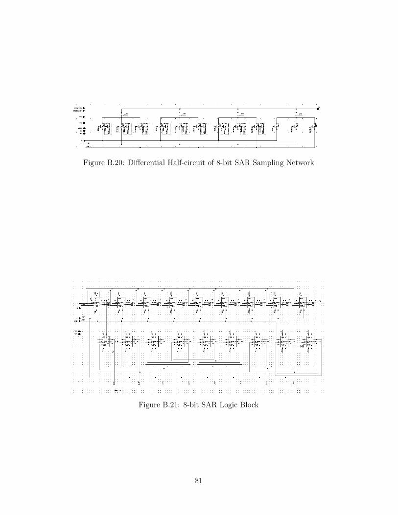
Figure B.20: Differential Half-circuit of 8-bit SAR Sampling Network
Figure B.21: 8-bit SAR Logic Block
81

B.4 16-channel Time-interleaved 8-Bit SAR ADC
Schematics
Figure B.22: Top-level Test-bench Schematic for 16-channelTime-interleaved 8-bit SAR ADC
82