Embed Size (px)
Citation preview

c© 2012 Youngseok Kim
PSEUDOSPIN TRANSFER TORQUES AND THE EFFECT OFDISORDER IN SEMICONDUCTOR ELECTRON BILAYERS
BY
YOUNGSEOK KIM
THESIS
Submitted in partial fulfillment of the requirementsfor the degree of Master of Science in Electrical and Computer Engineering
in the Graduate College of theUniversity of Illinois at Urbana-Champaign, 2012
Urbana, Illinois
Adviser:
Assistant Professor Matthew J. Gilbert
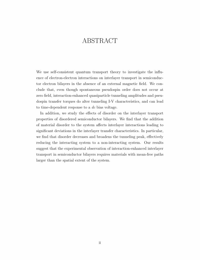
ABSTRACT
We use self-consistent quantum transport theory to investigate the influ-
ence of electron-electron interactions on interlayer transport in semiconduc-
tor electron bilayers in the absence of an external magnetic field. We con-
clude that, even though spontaneous pseudospin order does not occur at
zero field, interaction-enhanced quasiparticle tunneling amplitudes and pseu-
dospin transfer torques do alter tunneling I-V characteristics, and can lead
to time-dependent response to a dc bias voltage.
In addition, we study the effects of disorder on the interlayer transport
properties of disordered semiconductor bilayers. We find that the addition
of material disorder to the system affects interlayer interactions leading to
significant deviations in the interlayer transfer characteristics. In particular,
we find that disorder decreases and broadens the tunneling peak, effectively
reducing the interacting system to a non-interacting system. Our results
suggest that the experimental observation of interaction-enhanced interlayer
transport in semiconductor bilayers requires materials with mean-free paths
larger than the spatial extent of the system.
ii
To my parents, for their love and support
iii

ACKNOWLEDGMENTS
I would like to express my deep gratitude to my thesis adviser Prof. Matthew
J. Gilbert who made the whole work possible. I appreciate his strong encour-
agement and insightful guidance in my graduate study. I thank him also for
his patience on my slow progress and giving me opportunities to interact
with great researchers outside the university.
I would also like to thank Prof. Allan H. MacDonald (University of Texas-
Austin) for many useful insights on the theoretical aspects of this particular
project. I also thank Brian Dellabetta for his initial setup on the simulation
program and many useful discussions.
I am extremely grateful to the Fulbright Foundation for financial support
on my study as well as for several conference trips. The Fulbright Foundation
provided me a unique opportunity to interact with invaluable individuals
from all over the world.
Finally, I would like to thank my parents and my sister, whose love and
support throughout my academic career has been invaluable.
This work was supported by the Army Research Office.
iv
TABLE OF CONTENTS
CHAPTER 1 INTRODUCTION . . . . . . . . . . . . . . . . . . . . 11.1 Two-Dimensional Electron Gas . . . . . . . . . . . . . . . . . 11.2 Self-consistency in the Interacting System . . . . . . . . . . . 21.3 Interacting Bilayer System with Zero Field . . . . . . . . . . . 41.4 Figure . . . . . . . . . . . . . . . . . . . . . . . . . . . . . . . 5
CHAPTER 2 NON-EQUILIBRIUM GREEN’S FUNCTION . . . . . 62.1 Introduction . . . . . . . . . . . . . . . . . . . . . . . . . . . . 62.2 Retarded Green’s Function . . . . . . . . . . . . . . . . . . . . 72.3 Observables . . . . . . . . . . . . . . . . . . . . . . . . . . . . 82.4 Figure . . . . . . . . . . . . . . . . . . . . . . . . . . . . . . . 10
CHAPTER 3 PSEUDOSPIN TORQUE THEORY IN THE SEMI-CONDUCTOR BILAYER SYSTEM . . . . . . . . . . . . . . . . . 113.1 System Hamiltonian . . . . . . . . . . . . . . . . . . . . . . . 113.2 Pseudospin Transfer Torque Theory . . . . . . . . . . . . . . . 143.3 Simulation Details . . . . . . . . . . . . . . . . . . . . . . . . 163.4 Results and Discussions . . . . . . . . . . . . . . . . . . . . . 173.5 Figures . . . . . . . . . . . . . . . . . . . . . . . . . . . . . . . 21
CHAPTER 4 THE EFFECT OF DISORDER IN THE SEMI-CONDUCTOR BILAYER SYSTEM . . . . . . . . . . . . . . . . . 274.1 Modeling of Disorder . . . . . . . . . . . . . . . . . . . . . . . 274.2 Simulation Details . . . . . . . . . . . . . . . . . . . . . . . . 284.3 Results and Discussions . . . . . . . . . . . . . . . . . . . . . 294.4 Figures . . . . . . . . . . . . . . . . . . . . . . . . . . . . . . . 33
CHAPTER 5 CONCLUSION . . . . . . . . . . . . . . . . . . . . . . 35
REFERENCES . . . . . . . . . . . . . . . . . . . . . . . . . . . . . . . 37
v
CHAPTER 1
INTRODUCTION
1.1 Two-Dimensional Electron Gas
The first seminal paper of Fowler et al. [1] reported the low-temperature
electron transport measurement on a silicon metal-oxide-semiconductor field-
effect transistor (MOSFET). In their experiment, the electron is confined at
the interface between a silicon substrate and a gate oxide. Further experiment
[2] gave a first evidence on the existence of the 2D states at the semiconductor
interface. Aided by the development of the modulation doping [3] with δ-
doping method [4], it is found that the high quality sample of GaAs/AlGaAs
supports two-dimensional electron gas (2DEG) whose mobility is as high as
106 cm2/V s [5]. The finding of the “flatland” in the GaAs/AlGaAs system
has opened abundant possibilities of finding interesting phenomena. One of
the most exciting findings came from a simple low-temperature transport
measurement under large magnetic field, which is the quantum Hall effect
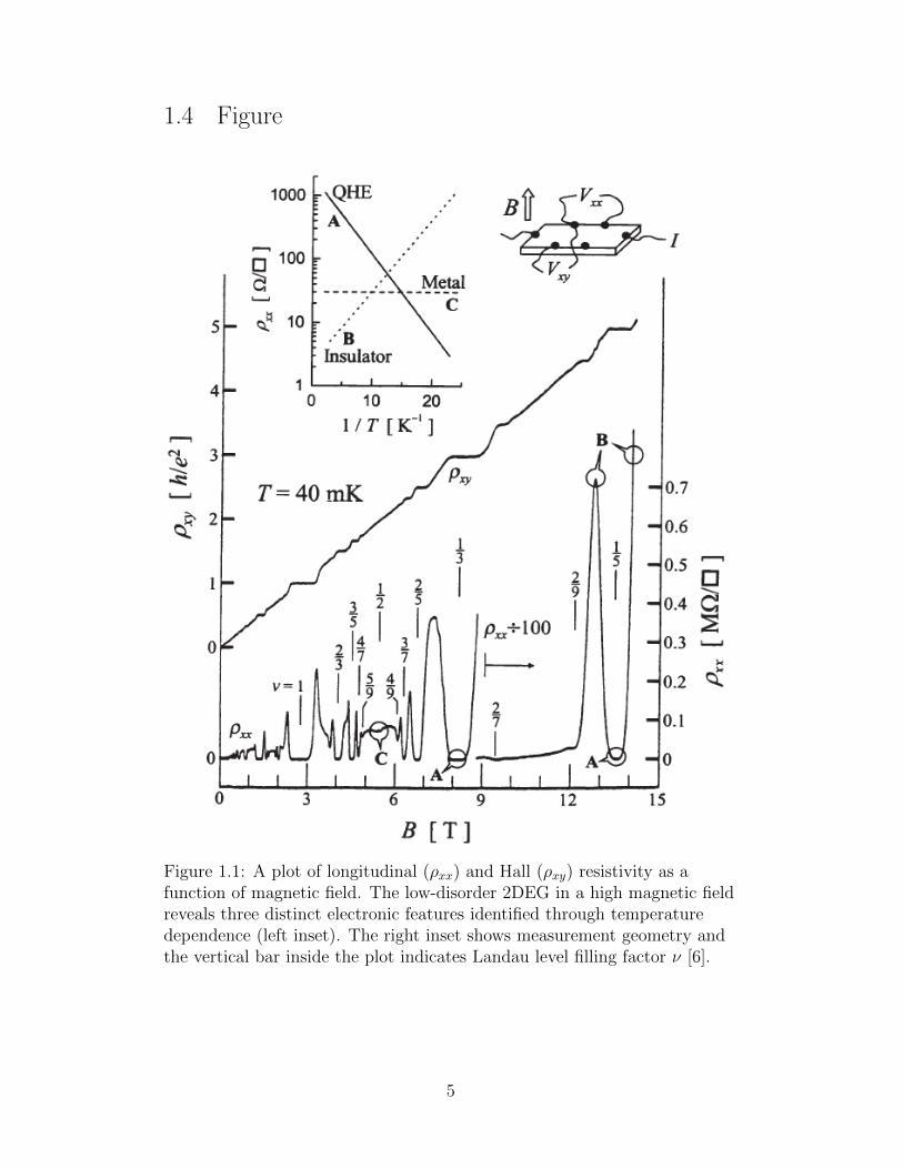
(QHE). Figure 1.1 (all figures are placed at the end of chapters) shows a
longitudinal (ρxx) and Hall (ρxy) resistivity at a particular Landau level filling
factor ν (vertical marking in the graph) [6]. Surprisingly, the ρxx drops
exponentially and approaches zero as temperature goes to zero at a certain
magnetic field (marked as A). Meanwhile, the system exhibits exponentially
increasing resistance with decreasing temperature at a certain magnetic field
(marked as B). As a result, simply by changing the field, one can tune the
system to have ground states of either metallic or insulating nature. This
astonishing phenomenon led to two physics Nobel prizes, one for the integer
QHE (IQHE), and the other for the fractional QHE (FQHE).
In addition to the IQHE and FQHE, an interesting feature at ν = 1/2
has attracted a number of researchers’ attention. In general, it is possible
to transform empty states as holes using the particle-hole transformation
1
[7, 8] and keep track of the empty states of a Landau level. Interestingly, at
half filling factor ν = 1/2, the electron layer can be transformed as the hole
layer with the same density. The same argument is applied to the bilayer
electron system which supports two adjoint 2DEGs registered between a thin
barrier. The bilayer system possesses both interlayer and intralayer electron-
electron interaction and this additional layer degrees of freedom leads to
unique characteristics. When the system has equal densities of two 2DEGs
with ν = 1/2, the strong interlayer interaction induces spontaneous interlayer
phase coherence. As a result, the system has exotic insulating states called
exciton condensation [9, 10]. The exciton condensate transition occurs where
the interlayer as well as intralayer interaction are dominant and is signaled
by a huge enhancement in the tunneling rate [9, 11]. The bilayer system leads
to a number of interesting experimental results such as interlayer transport
anomalies [11, 12] and a signature of dissipationless transport [13, 14]. As
a consequence, the bilayer system has served as a test bed for many-body
physics for the past two decades.
1.2 Self-consistency in the Interacting System
As we discussed in the previous section, interesting phenomena are found
in the presence of strong interactions. Thus, how to model and evaluate
the interacting system properly is an important question. When interaction
effects are neglected a nanoscale conductor always reaches a steady state
[15] in which current increases smoothly with bias voltage. This problem is
efficiently solved using Green’s function techniques, for example, by using
the non-equilibrium Green’s function (NEGF) method [15]. Real electrons
interact, of course, and the free-fermion degrees of freedom which appear
in this type of theory should always be thought of as Fermi liquid theory
[16, 17, 18] quasiparticles. The effective single-particle Hamiltonian there-
fore depends on the microscopic configuration of the system. In practice the
quasiparticle Hamiltonian is often [19, 20] calculated from a self-consistent
mean-field theory like Kohn-Sham density functional theory (DFT). DFT,
spin-density functional theory, current-density functional theory, Hartree the-
ory, and Hartree-Fock theory all function as useful fermion self-consistent-
field theories. Since a bias voltage changes the system density matrix, it in-
2
evitably changes the quasiparticle Hamiltonian. Determination of the steady
state density matrix therefore requires a self-consistent calculation.
Self-consistency is included routinely in NEGF simulations [21, 22, 23] of
transport at the Hartree theory level in nanoscale semiconductor systems and
in simulations [24, 25, 26, 27, 28] of molecular transport. The collective be-
havior captured by self-consistency can sometimes change the current-voltage
relationship in a qualitative way, leading to an I-V curve that is not smooth
or even to circumstances in which there is no steady state response to a time-
independent bias voltage. Some of the most useful and interesting examples
of this type of effect occur in ferromagnetic metal spintronics. The quasipar-
ticle Hamiltonian is a ferromagnetic metal that has a large spin-splitting term
which lowers the energy of quasiparticles whose spins are aligned with the
magnetization (majority-spin quasiparticles) relative to those quasiparticles
whose spins are aligned opposite to the magnetization (minority-spin quasi-
particles). When current flows in a ferromagnetic metal the magnetization di-
rection is altered [29]. The resulting change in the quasiparticle Hamiltonian
[29] is responsible for the rich variety of so-called spin-transfer torque collec-
tive transport effects which occur in magnetic metals and semiconductors.
These spin-transfer torques [30, 31] are often understood macroscopically1 as
the reaction counterpart of the torques which act on the quasiparticle spins
that carry current through a non-collinear ferromagnet. Spin-transfer torques
[30] can lead to discontinuous I-V curves and to oscillatory [32] or chaotic
response to a time-independent bias voltage. Similar phenomena [33] occur
in semiconductor bilayers for certain ranges of external magnetic field over
which the ground state has spontaneous [34, 10, 9] interlayer phase coher-
ence (see Section 1.1). Indeed when bilayer exciton condensate ordered states
are viewed as pseudospin ferromagnets, the spectacular transport anomalies
[9, 11, 35, 36, 12] they exhibit have much in common with those of ferromag-
netic metals.
1The microscopic and macroscopic pictures are essentially equivalent in ferromagnetsbecause the spin-splitting term is much larger than other spin-dependent terms in thequasiparticle Hamiltonian.
3
1.3 Interacting Bilayer System with Zero Field
In this thesis we address interlayer transport in separately contacted nanome-
ter length scale semiconductor bilayers, with a view toward the identification
of possible interaction-induced collective transport effects. In particular, we
consider semiconductor bilayers at zero magnetic field, using a pseudospin
language [37, 38] in which top layer electrons are said to have pseudospin up
(| ↑〉) and bottom layer electrons are said to have pseudospin down (| ↓〉).Although interlayer transport in semiconductor bilayers has been studied
extensively in the strong field quantum Hall regime, work on the zero field
limit has been relatively sparse and has focused on studies of interlayer drag
[39, 40, 41, 42], counterflow [43], and on speculations about possible broken
symmetry states [44, 45]. We concur with the consensus view that pseu-
dospin ferromagnetism is not expected in conduction band two-dimensional
electron systems2 [46] except possibly [47] at extremely low carrier densi-
ties. There are nevertheless pseudospin-dependent interaction contributions
to the quasiparticle Hamiltonian. When a current flows, the pseudospin ori-
entation of transport electrons is altered, just as in metal spintronics, and
some of the same phenomena can occur. The resulting change in the quasi-
particle Hamiltonian is responsible for a current-induced pseudospin-torque
which alters the state of non-transport electrons well away from the Fermi
energy. Indeed although the spin-splitting field appears spontaneously in
ferromagnetic metals, spintronics phenomena usually depend on an inter-
play between the spontaneous exchange field and effective magnetic fields
due to magnetic-dipole interactions, spin-orbit coupling, and external mag-
netic fields. In semiconductor bilayers the pseudospin external field is due
to single-particle interlayer tunneling amplitude and is typically of the same
order [48] as the interaction contribution to the pseudospin-splitting field.
While theoretically possible and potentially useful as a logic device [49], to
be experimentally observed, these pseudospin exchange field signatures must
be robust against material disorder, which these semiconductor bilayer sys-
tems are well-known to contain. Therefore, understanding the observable
deviations in interlayer transport caused by material disorder is also studied.
2Pseudospin ferromagnetism (or equivalently exciton condensation) is, however, pre-dicted in systems with equal densities of conduction band electrons and valence band holesin separate quantum wells.
4
1.4 Figure
Figure 1.1: A plot of longitudinal (ρxx) and Hall (ρxy) resistivity as afunction of magnetic field. The low-disorder 2DEG in a high magnetic fieldreveals three distinct electronic features identified through temperaturedependence (left inset). The right inset shows measurement geometry andthe vertical bar inside the plot indicates Landau level filling factor ν [6].
5
CHAPTER 2
NON-EQUILIBRIUM GREEN’S FUNCTION
2.1 Introduction
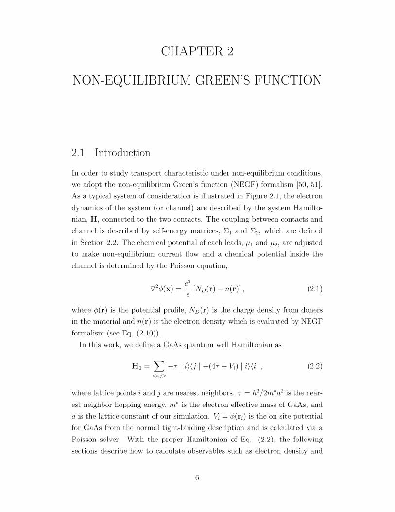
In order to study transport characteristic under non-equilibrium conditions,
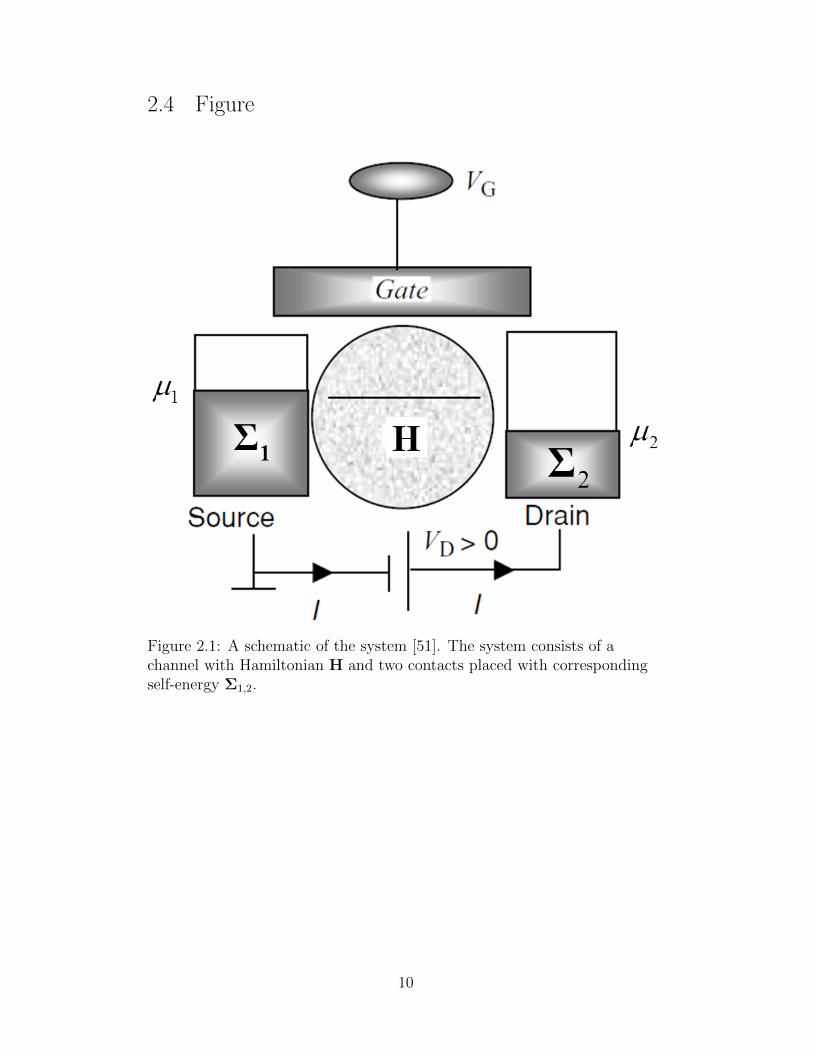
we adopt the non-equilibrium Green’s function (NEGF) formalism [50, 51].
As a typical system of consideration is illustrated in Figure 2.1, the electron
dynamics of the system (or channel) are described by the system Hamilto-
nian, H, connected to the two contacts. The coupling between contacts and
channel is described by self-energy matrices, Σ1 and Σ2, which are defined
in Section 2.2. The chemical potential of each leads, µ1 and µ2, are adjusted
to make non-equilibrium current flow and a chemical potential inside the
channel is determined by the Poisson equation,
O2φ(x) =e2
ε[ND(r)− n(r)] , (2.1)
where φ(r) is the potential profile, ND(r) is the charge density from doners
in the material and n(r) is the electron density which is evaluated by NEGF
formalism (see Eq. (2.10)).
In this work, we define a GaAs quantum well Hamiltonian as
H0 =∑<i,j>
−τ | i〉〈j | +(4τ + Vi) | i〉〈i |, (2.2)
where lattice points i and j are nearest neighbors. τ = ~2/2m∗a2 is the near-
est neighbor hopping energy, m∗ is the electron effective mass of GaAs, and
a is the lattice constant of our simulation. Vi = φ(ri) is the on-site potential
for GaAs from the normal tight-binding description and is calculated via a
Poisson solver. With the proper Hamiltonian of Eq. (2.2), the following
sections describe how to calculate observables such as electron density and
6
current via NEGF formalism.
2.2 Retarded Green’s Function
Within the NEGF formalism, we define the retarded Green’s function as
below [50, 51]
G(E) =[(E + i0+) I−H0 −Σ1(E)−Σ2(E)
]−1, (2.3)
where 0+ is an infinitesimal positive number, I is the identity matrix and
H0 is the system Hamiltonian in Eq. (2.2). In order to complete the above
definition, we need to define Σ1(2)(E), which is a self-energy function of the
semi-infinite contact 1 (2). Although we assume contacts are semi-infinite,
we can devide the contact system by blocks with a contact Hamiltonian, Hc,
and a hopping matrix between blocks, τc. Then, the surface Green’s function,
gs, is defined as
gs =[(E + i0+) I−Hc − τcHcτ
†c
]−1. (2.4)
As a result, the self-energy of the contact is defined as,
Σ(E) = τcpgsτ†cp, (2.5)
where τcp is a coupling matrix between channel and contact. The broadening
matrix due to the contact is obtained from the imaginary part of the self-
energy,
Γ = i(Σ−Σ†) (2.6)
whose meaning is the rate at which carriers are injected into the channel.
In case we have two contacts as in Figure 2.1, we define the self-energy, Σ1
and Σ2, and the broadening matrix, Γ1 and Γ2, for the contact 1 and 2,
respectively.
7
2.3 Observables
With the definitions in Section 2.1 and 2.2, the transmission is defined as
T12(E) = Trace[Γ1GΓ2G
†] = Trace[Γ2GΓ1G
†] . (2.7)
When we consider the coherent transport inside the channel, the terminal
current is calculated by the Landauer formula:
I =e
h
∫dE T12(E) (f1(E)− f2(E)) , (2.8)
where f1, f2 are Fermi-Dirac distribution of each contacts. As long as we
only consider the interaction between the system and each lead, the inscat-
tering and outscattering function is defined solely by contact self-energy as
Σin(E) =∑
p fp(E)Σp and Σout(E) =∑
p(1− fp(E))Σp, where p runs over
contacts which are connected to the system [50]. As a result, we can define
electron (hole) correlation function, Gn (Gp), as
Gn = GΣinG†, Gp = GΣoutG†. (2.9)
Using the electron and hole correlation function in Eq. (2.9), the electron
and hole density are defined as below,
n =
∫dE
2πGn(E), p =
∫dE
2πGp(E). (2.10)
For example, the matrix expression of the one-dimensional system described
by Eq. (2.2) is
H0 =
4τ + V1 −τ 0 · · · 0
−τ 4τ + V2 −τ · · · 0...
......
......
0 0 · · · −τ 4τ + VN
, (2.11)
8
and the corresponding density matrix from Eq. (2.10) is
n =
ρ11 ρ12 ρ13 · · · ρ1N
ρ21 ρ22 ρ23 · · · ρ2N
......
......
...
ρN1 ρN2 ρN3 · · · ρNN
. (2.12)
As the n (or p) in Eq. (2.12) is a matrix, it is possible to obtain on-site density
from diagonal elements as well as off-diagonal terms which will be used to
evaluate interlayer interaction in the case of the semiconductor bilayer system
(for detail, see Eq. (3.4) and the following discussion in Chapter 3.1.1). Then,
the electron (or hole) density at a certain bias condition is fed back to the
Poisson solver to obtain Vi in Eq. (2.2) and observables are calculated after
this self-consistent loop is converged within a defined tolerance.
9
2.4 Figure
Figure 2.1: A schematic of the system [51]. The system consists of achannel with Hamiltonian H and two contacts placed with correspondingself-energy Σ1,2.
10
CHAPTER 3
PSEUDOSPIN TORQUE THEORY IN THESEMICONDUCTOR BILAYER SYSTEM
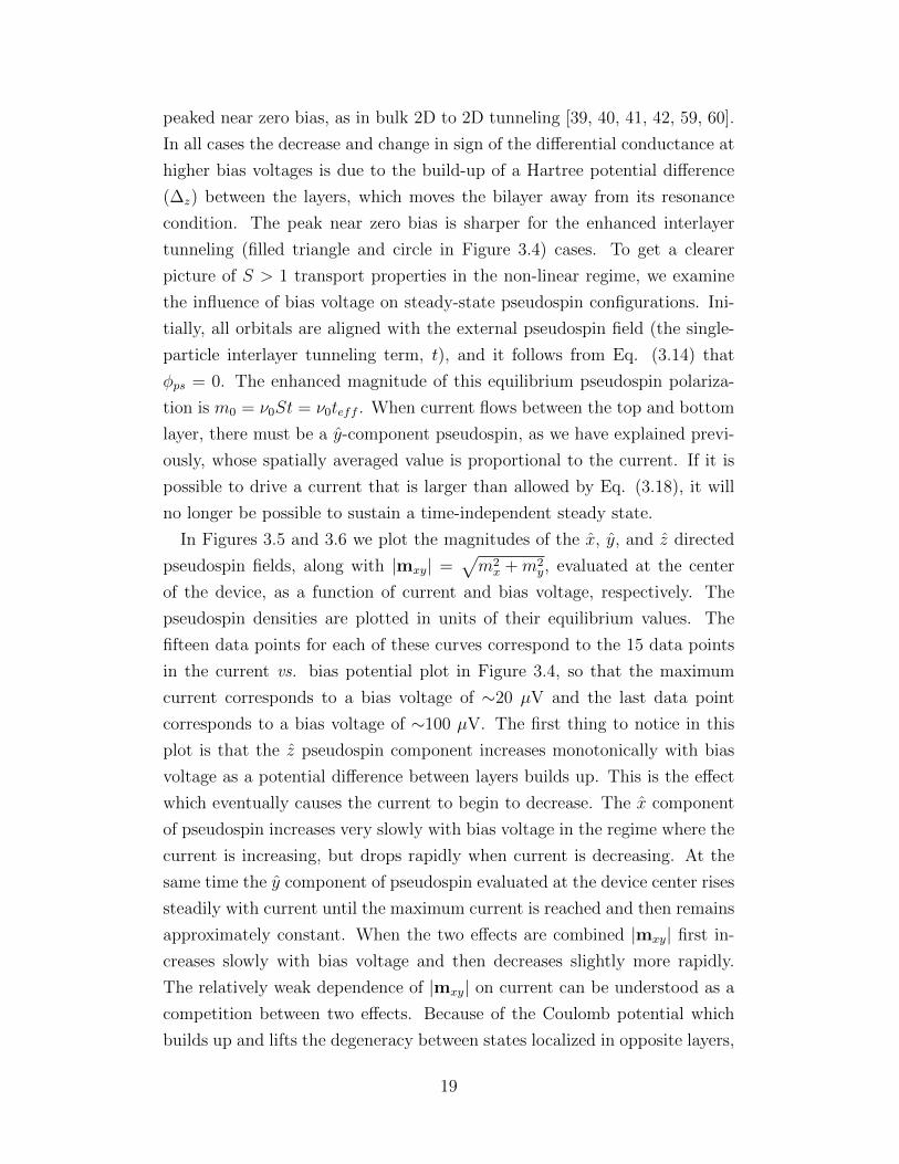
We consider an Al0.9Ga0.1As/GaAs bilayer heterostructure with top and bot-
tom Al0.9Ga0.1As barriers which act to isolate the coupled quantum wells from
electrostatic gates, as illustrated in Figure 3.1a. The bilayer consists of two
15 nm deep GaAs quantum wells with an assumed 2DEG electron density
of 2.0× 1010 cm−2 separated by a 1 nm Al0.9Ga0.1As barrier. The quantum
wells are 1.2 µm long and 7.5 µm wide with the splitting between the sym-
metric and antisymmetric states set to a small value ∆SAS = 2t = 2 µeV.
We define the z-axis as the growth direction, the x-axis as the longitudinal
(transport) direction, and the y-axis as the direction across the transport
channel as shown schematically in Figure 3.1a. We connect ideal contacts
attached to the inputs and outputs of both layers. The contacts inject and
extract current and enter into the Hamiltonian via appropriate self-energy
terms [15].
3.1 System Hamiltonian
In the following sections, we begin this chapter by formulating the system
Hamiltonian considering the interlayer exchange interaction with pseudospin
language.
3.1.1 Interacting System Hamiltonian
We construct the system Hamiltonian from a model with a single-band effec-
tive mass Hamiltonian for top and bottom layers with a phenomenological
11
single-particle inter-layer tunneling term:
H =
[HTL 0
0 HBL
]+∑
µ=x,y,z
µ ·∆⊗ σµ. (3.1)
The first term on the right-hand side of Eq. (3.1) is the single-particle non-
interacting term while the second term is a mean-field interaction term. In
the first term in the right-hand side, HTL and HBL are an individual quan-
tum well Hamiltonian, H0, which is described in Eq. (2.2). In the second
term in the right-hand side, σµ represents the Pauli spin matrices in each
of the three spatial directions µ = x, y, z, ⊗ represents the Kronecker prod-
uct, and ∆ is a pseudospin effective magnetic field which will be discussed
in more detail later in this section. To explore interaction physics in bilayer
transport qualitatively, we use a local density approximation in which the in-
teraction contribution to the quasiparticle Hamiltonian is proportional to the
pseudospin-magnetization at each point in space. If we take the top layer as
the pseudospin up state (| ↑〉) and the bottom layer as the pseudospin down
state (| ↓〉), the single-particle interlayer tunneling term contributes a pseu-
dospin effective field with magnitude t = ∆SAS/2 and direction x. In real spin
ferromagnetic systems, interactions between spin-polarized electrons lead to
an effective magnetic field in the direction of spin-polarization. Bilayers with
pseudospin-polarization due to tunneling have a similar interaction contri-
bution to the quasiparticle Hamiltonian. Including both single-particle and
many-body interaction contributions, the pseudospin effective field ∆ term
in the quasiparticle Hamiltonian is [52, 37],
∆ = (t+ Umxps) x+ Umy
ps y (3.2)
where the pseudospin-magnetization mps is defined by
mps =1
2Tr[ρpsτ ]. (3.3)
In Eq. (3.3), τ = σx, σy, σz is the vector of Pauli spin matrices, and ρps is
the 2× 2 Hermitian pseudospin density matrix which we define as,
ρps =
[ρ↑↑ ρ↑↓
ρ↓↑ ρ↓↓
]. (3.4)
12
The diagonal terms of the pseudospin density matrix (ρ↑↑, ρ↓↓) are the elec-
tron densities of the top and bottom layers. In Eq. (3.2), we have dropped the
exchange potential associated with the z component of pseudospin because
it is dominated by the electric potential difference between layers induced
by the interlayer bias voltage (see below). From the definition of Eq. (3.3),
the pseudospin-magnetization of x, y, z directions are defined in terms of the
density matrix as
〈mxps〉 =
1
2(ρ↑↓ + ρ↓↑),
〈myps〉 =
1
2(−iρ↑↓ + iρ↓↑),
〈mzps〉 =
1
2(ρ↑↑ − ρ↓↓).
(3.5)
Using Eqs. (3.2) and (3.5), we may express the system Hamiltonian in terms
of pseudospin field contributions,
H =
[HTL + ∆z ∆x − i∆y
∆x + i∆y HBL −∆z
]. (3.6)
Here ∆z is the electric potential difference between the two layers which we
evaluate in a Hartree approximation, disregarding its exchange contribution.
The planar pseudospin angle which figures prominently in the discussion
below is defined by
φps = tan−1
(〈myps〉
〈mxps〉
). (3.7)
This angle corresponds physically to the phase difference between electrons
in the two layers.
3.1.2 Enhanced Interlayer Tunneling
With the quasiparticle Hamiltonian for our semiconductor bilayer defined, we
now address the strength of the interlayer interactions present in the system.
The interaction parameter U in Eq. (3.2) is chosen so that the local density
approximation for interlayer exchange reproduces a prescribed value for the
interaction enhancement of the interlayer tunneling amplitude. In equilib-
rium the pseudospin magnetization will be oriented in the x direction and
13
the quasiparticle will have either symmetric or antisymmetric bilayer states
with pseudospins in the x and −x-directions, respectively. The majority and
minority pseudospin states differ in energy at a given momentum by 2teff
where
teff = t+ UNs −Na
2. (3.8)
The population difference between symmetric and antisymmetric differences
may be evaluated from the differences in their Fermi radii illustrated in Figure
3.2:Ns −Na
2= ν0 teff , (3.9)
where ν0 is the density-of-states of a single layer. Combining Eq. (3.8) and
Eq. (3.9) we can relate U to S, the interaction enhancement factor for the
interlayer tunneling amplitude:
teff =t
1− Uν0
≡ S t. (3.10)
The physics of S is similar to that responsible for the interaction enhancement
of the Pauli susceptibility in metals. According to microscopic theory [48]
a typical value for S is around 2. We choose to use S rather than U as a
parameter in our calculations and therefore set
U =1− S−1
ν0
' 1
2ν0
. (3.11)
3.2 Pseudospin Transfer Torque Theory
In the following section we report on simulations in which we drive an in-
terlayer current by keeping the top left and top right contacts grounded and
applying identical interlayer voltages, VINT , at the bottom left and bottom
right contacts. We choose this bias configuration so as to focus on interlayer
currents that are relatively uniform. The transport properties depend only
on the quasiparticle Hamiltonian and on the chemical potentials in the leads.
Because the pseudospin effective field is the only term in the quasiparticle
Hamiltonian which does not conserve the z component of the pseudospin, it
14
follows that every quasiparticle wavefunction in the system must satisfy [53]
∂tmzps = −∇ · jz − 2
~(mps ×∆)z = 0 (3.12)
where jz is the z component of the pseudospin current contribution from that
orbital, i.e. the difference between bottom and top layer number currents,
and mps is the pseudospin magnetization of that orbital. For steady state
transport, the quasiparticles satisfy time-independent Schrodinger equations
so that, summing over all quasiparticle orbitals, we find,
2|mps||∆| sin(φps − φ∆) = 2tmyps = ~∇ · jz. (3.13)
In Eq. (3.13), φ∆ is the planar orientation of ∆. The first equality in Eq.
(3.13) follows from Eq. (3.2). The pseudospin orbitals do not align with the
effective field they experience because they must precess between layers as
they transverse the sample. The realignment of transport orbital pseudospin
orientations alters the total pseudospin and therefore the interaction contri-
bution to ∆. The change in mps×∆ due to transport currents is referred to
here as the pseudospin transfer torque, in analogy with the terminology com-
monly found in metal spintronics. Integrating Eq. (3.13) across the sample
from left to right and accounting for spin degeneracy, we find that
4etA〈myps〉
~= IL + IR = I (3.14)
where A is the 2D layer area, the angle brackets denote a spatial average, and
IL and IR are the currents flowing from top to bottom at the left and right
contacts. (The pseudospin current jz flows to the right on the right and is
positive on the right side of the sample, but flows to the left and is negative
on the left side of the sample.) If the bias voltage can drive an interlayer
current I larger than 4etA〈myps〉/~, it will no longer be possible to achieve
a transport steady state. Under these circumstances the interlayer current
will oscillate in sign and the time-averaged current will be strongly reduced.
In the next section we use a numerical simulation to assess the possibility of
achieving currents of this size.
A similar conclusion can be reached following a different line of argument.
The microscopic operator J describing net current flowing top layer (↑) to
15
bottom layer (↓) given by [42, 54] is
J =−iet~∑k,σ
(c†k,σ,↑ck,σ,↓ − c
†k,σ,↓ck,σ,↑
)=−2et
~i∑k
(c†k,↑ck,↓ − c
†k,↓ck,↑
)=
4et
~myps,
(3.15)
where k, σ are the momentum and spin indices, respectively. Here we have
introduced a common notation ∆SAS = 2t for the pseudospin splitting be-
tween symmetric and antisymmetric states in the absence of interactions and
added a factor of 2 to account for spin-degeneracy. The pseudospin density
operator myps in Eq. (3.15) is given by
myps =
−i2
∑k
(c†k,↑ck,↓ − c
†k,↓ck,↑
). (3.16)
As a result, current density flowing in the given system may be written as⟨J⟩
=4et
~⟨myps
⟩=
4et
~|mxy| sinφ
≤ 4et
~|mxy| = Jc,
(3.17)
where |mxy| =√〈mx〉2 + 〈my〉2, φps is defined in Eq. (3.7) and Jc is defined
as a critical current density. Assuming the current flow is uniform across the
device, it is possible to obtain the critical current simply by multiplying Eq.
(3.17) by the system area A to obtain
Ic = Jc × A =4etA
~|mxy|. (3.18)
3.3 Simulation Details
As we neglect disorder in this simulation, we may write the Hamiltonian in
the form of decoupled 1D longitudinal channels in the transport (x) direction,
taking proper account of the eigenenergy of transverse (y) direction motion
16
[55]. The calculation strategy follows a standard self-consistent field proce-
dure as is described in a flow chart of Figure 3.1b. Given the density matrix
of the 1D system, we can evaluate the mean-field quasiparticle Hamiltonian.
For the interlayer tunneling part of the Hamiltonian, we use the local-density
approximation outlined in Section 3.1.2. The electrostatic potential in each
layer is calculated from the charge density in each of the layers by solving a
2D Poisson equation using an alternating direction implicit method [56] with
appropriate boundary conditions. The boundary conditions employed in this
situation were hard wall boundaries on the top and sides of the simulation
domain and Neumann boundaries at the points where current is injected to
insure charge neutrality [57]. Given the mean-field quasiparticle Hamiltonian
and voltages in the leads, we can solve for the steady state density matrix
of the two-dimensional bilayer using the NEGF method with a real-space
basis. The density-matrix obtained from the quantum transport calculation
is updated at each state in the iteration process. The update density is then
fed back into the Poisson solver and on-site potential is updated using the
Broyden method [58] to accelerate self-consistency. The effective interlayer
tunneling amplitudes are also updated and the loop proceeds until a desired
level of self-consistency is achieved. The transport properties are calculated
after self-consistency is achieved by applying the Landauer formula, i.e. by
using
I(Vsd) =2e
h
∫T (E)[fs(E)− fd(E)]. (3.19)
3.4 Results and Discussions
3.4.1 Linear Response
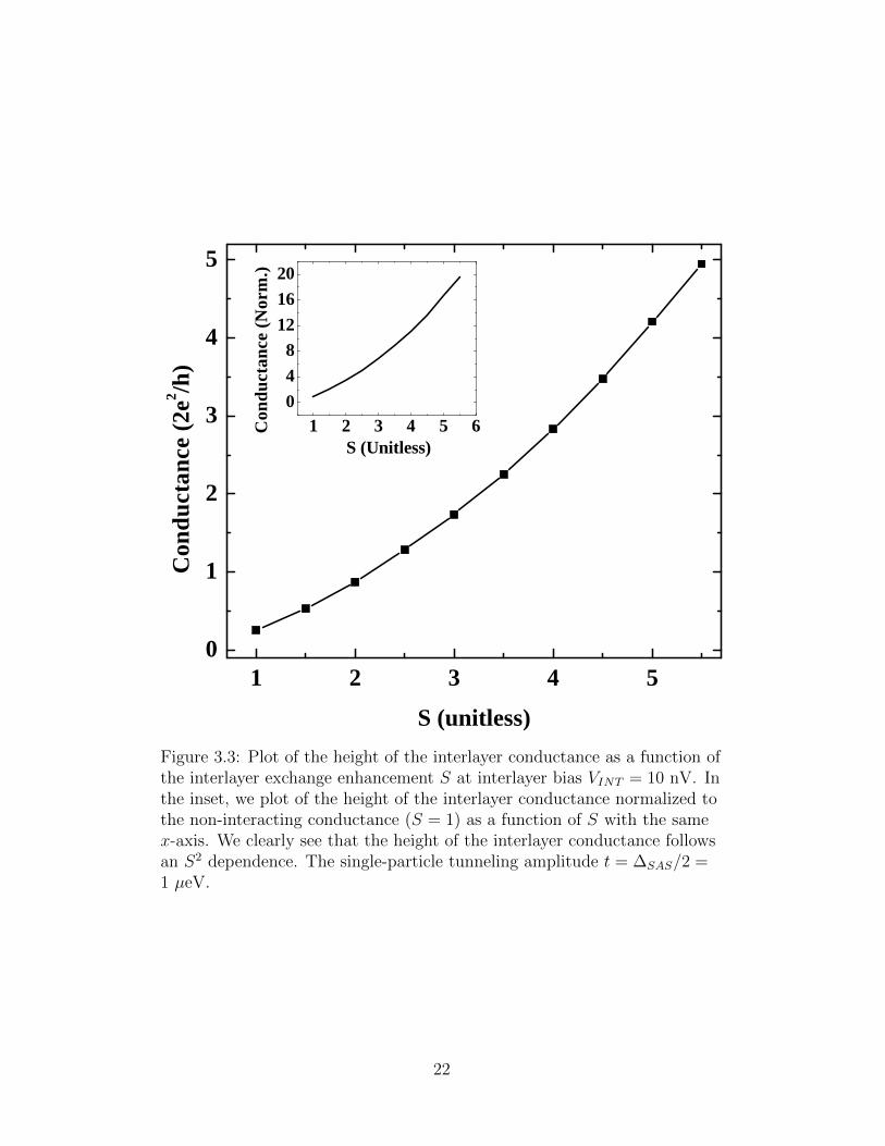
In Figure 3.3, we plot the interlayer conductance at temperature T = 0 as a
function of the interlayer exchange enhancement, S by setting VBL = VBR =
VINT and VTL = VTR = 0 in Figure 3.1a. The S2 dependence demonstrates
that the conductance in our nanodevice is proportional to the square of the
quasiparticle tunneling amplitude, as in bulk samples [39, 40, 41, 42, 59, 60],
and that the quasiparticle tunneling amplitude is approximately uniformly
enhanced even though the finite-size system is not perfectly uniform. The
range of S used in this figure corresponds to the relatively modest enhance-
17
ment factors that we expect in bilayer systems in which the individual layers
have the same sign of mass. For systems in which the quasiparticle masses
are opposite in the two layers, we expect values of S that are significantly
larger. Spontaneous interlayer coherence, which occurs in a magnetic field
[11, 61, 62, 63, 64] but is not expected in the absence of a field, would be
signaled by a divergence in S.
The physics of the results illustrated in Figure 3.3 can be understood qual-
itatively by ignoring the finite-size-related spatial inhomogeneities present in
our simulations and considering the simpler case in which there is a single
bottom-layer source contact and a single top-layer drain contact on opposite
ends of the transport channels. The interlayer tunneling is then diagonal
in a transverse channel, and the transmission probability from top layer to
bottom layer in channel k is
Tinterlayer = sin2
(δkL
2
). (3.20)
In Eq. (3.20), δk is the difference between the current direction wavevectors
of the symmetric and antisymmetric states and L is the system length in
the transport direction. We may simplify the expression in Eq. (3.20) by
rewriting it in terms of the Fermi velocity, vf , in the transport-direction and
making use of the small angle expansion of the sin function to obtain
Tinterlayer =
(teffL
~vf
)2
, (3.21)
where teff is the quasiparticle tunneling amplitude proportional to the inter-
layer exchange enhancement S, which results in the power law dependence
seen in Figure 3.3. As this approximate expression suggests, we find that
transport at low interlayer bias voltages is dominated by the highest energy
transverse channel, which has the smallest transport direction Fermi velocity.
3.4.2 Transport Beyond Linear Response
We have seen that at small bias voltages the inter-layer current is enhanced
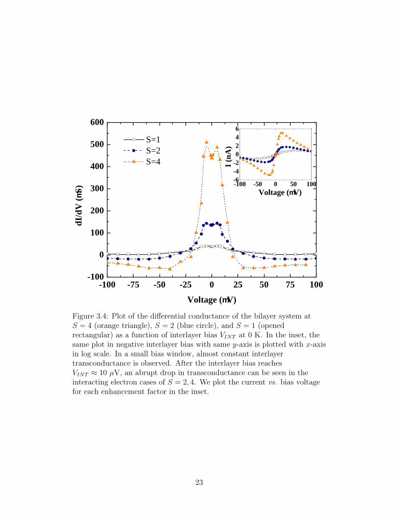
by interlayer exchange interactions. In Figure 3.4 , we compare our interlayer
transport result with the S = 1 case. We see that all of the curves are sharply
18
peaked near zero bias, as in bulk 2D to 2D tunneling [39, 40, 41, 42, 59, 60].
In all cases the decrease and change in sign of the differential conductance at
higher bias voltages is due to the build-up of a Hartree potential difference
(∆z) between the layers, which moves the bilayer away from its resonance
condition. The peak near zero bias is sharper for the enhanced interlayer
tunneling (filled triangle and circle in Figure 3.4) cases. To get a clearer
picture of S > 1 transport properties in the non-linear regime, we examine
the influence of bias voltage on steady-state pseudospin configurations. Ini-
tially, all orbitals are aligned with the external pseudospin field (the single-
particle interlayer tunneling term, t), and it follows from Eq. (3.14) that
φps = 0. The enhanced magnitude of this equilibrium pseudospin polariza-
tion is m0 = ν0St = ν0teff . When current flows between the top and bottom
layer, there must be a y-component pseudospin, as we have explained previ-
ously, whose spatially averaged value is proportional to the current. If it is
possible to drive a current that is larger than allowed by Eq. (3.18), it will
no longer be possible to sustain a time-independent steady state.
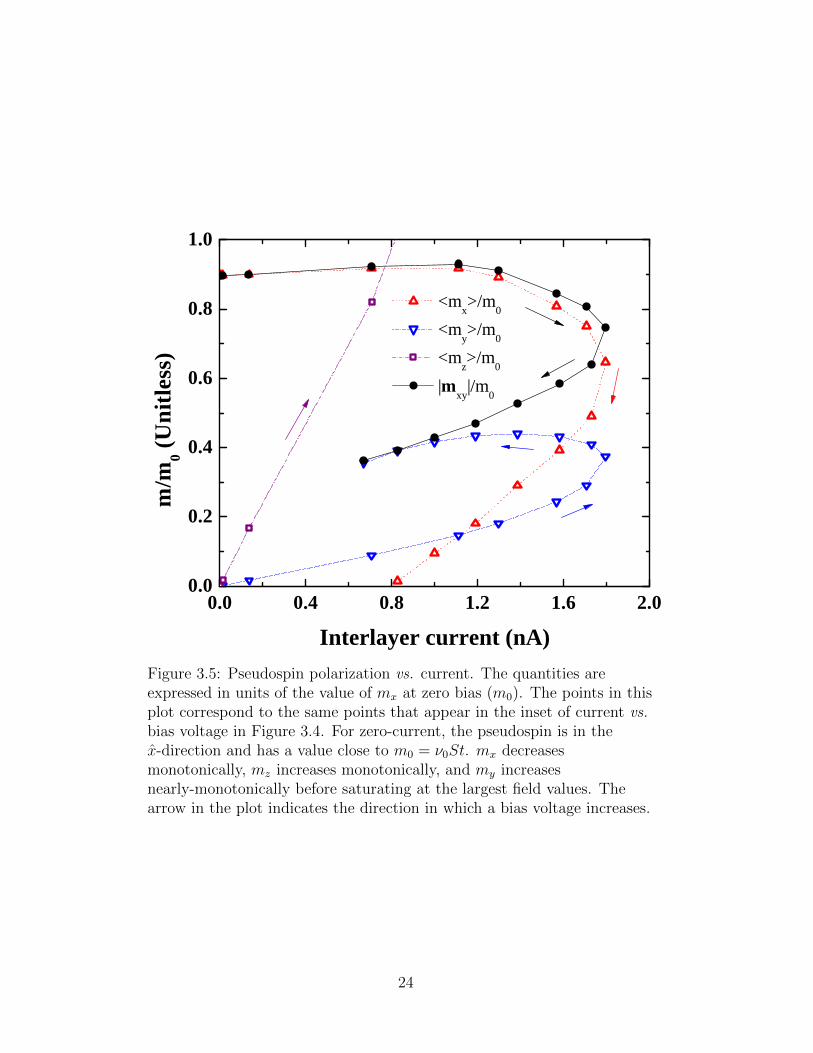
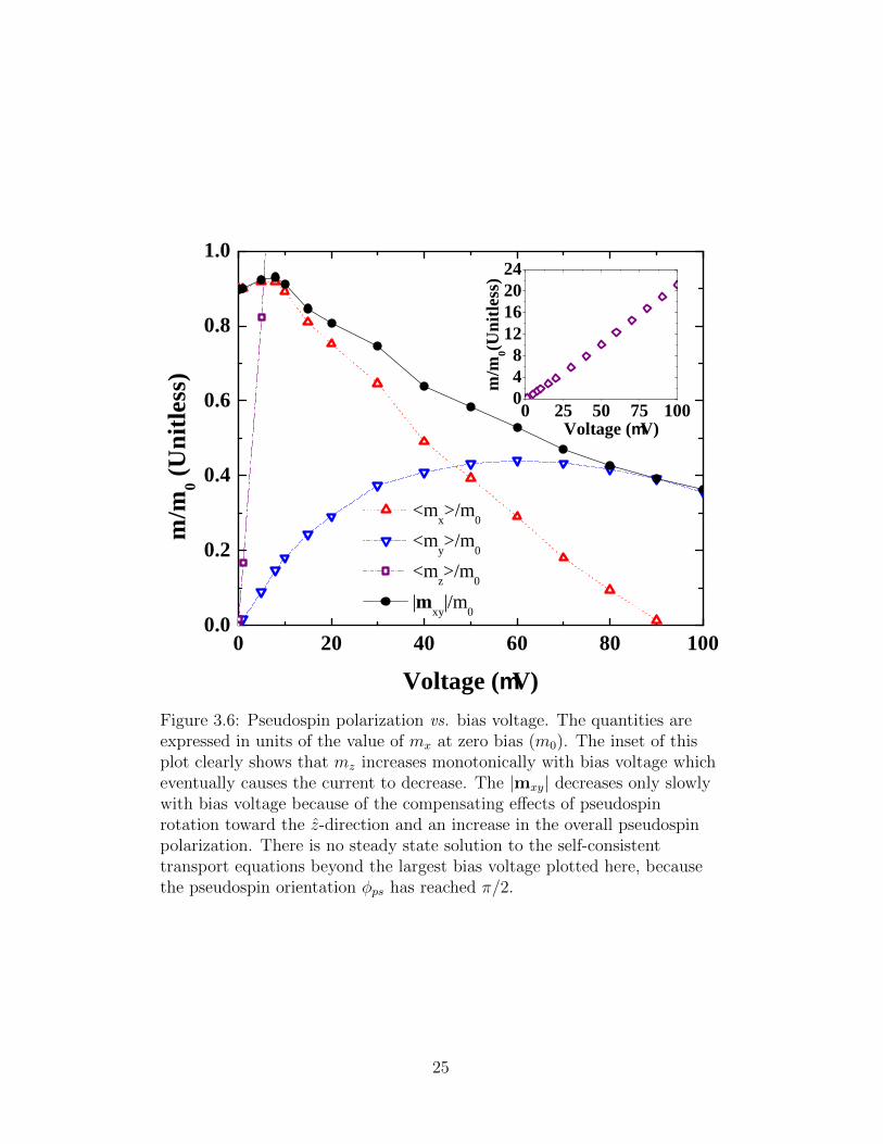
In Figures 3.5 and 3.6 we plot the magnitudes of the x, y, and z directed
pseudospin fields, along with |mxy| =√m2x +m2
y, evaluated at the center
of the device, as a function of current and bias voltage, respectively. The
pseudospin densities are plotted in units of their equilibrium values. The
fifteen data points for each of these curves correspond to the 15 data points
in the current vs. bias potential plot in Figure 3.4, so that the maximum
current corresponds to a bias voltage of ∼20 µV and the last data point
corresponds to a bias voltage of ∼100 µV. The first thing to notice in this
plot is that the z pseudospin component increases monotonically with bias
voltage as a potential difference between layers builds up. This is the effect
which eventually causes the current to begin to decrease. The x component
of pseudospin increases very slowly with bias voltage in the regime where the
current is increasing, but drops rapidly when current is decreasing. At the
same time the y component of pseudospin evaluated at the device center rises
steadily with current until the maximum current is reached and then remains
approximately constant. When the two effects are combined |mxy| first in-
creases slowly with bias voltage and then decreases slightly more rapidly.
The relatively weak dependence of |mxy| on current can be understood as a
competition between two effects. Because of the Coulomb potential which
builds up and lifts the degeneracy between states localized in opposite layers,
19
the direction of the pseudospin tilts toward the z direction, decreasing the
x− y plane component of each state. At the same time the total magnitude
of the pseudospin field increases, increasing the pseudospin polarization. In
a uniform system the two effects cancel when a z-direction pseudospin field
is added to a uniform system.
Our simulations suggest the following scenario for how the critical current
might be reached in bilayers. The width of the linear response regime is lim-
ited by the lifetime of Bloch states, which is set by disorder in bulk systems,
and in our finite-size system by the time for escape into the contacts. In the
linear-response regime the current is enhanced by a factor of S2 by inter-layer
exchange interactions. The maximum current which can be supported in the
steady state is however proportional to the bare inter-layer tunneling and to
the x− y pseudospin polarization and is therefore enhanced only by a factor
of S. From this comparison we can conclude that more strongly enhanced
inter-layer tunneling quasiparticle tunneling amplitudes (larger S) increases
the chances of reaching a critical current beyond which the system current
response is dynamic. For the parameters of our simulation, the maximum
current of around 4 nA is reached at a bias voltage of around 10 µV. At this
bias voltage the average x− y plane angle of the pseudospin field is still less
than 90◦, and steady state response occurs. As the bias voltage increases
further, the total current decreases, but the pseudospins become strongly
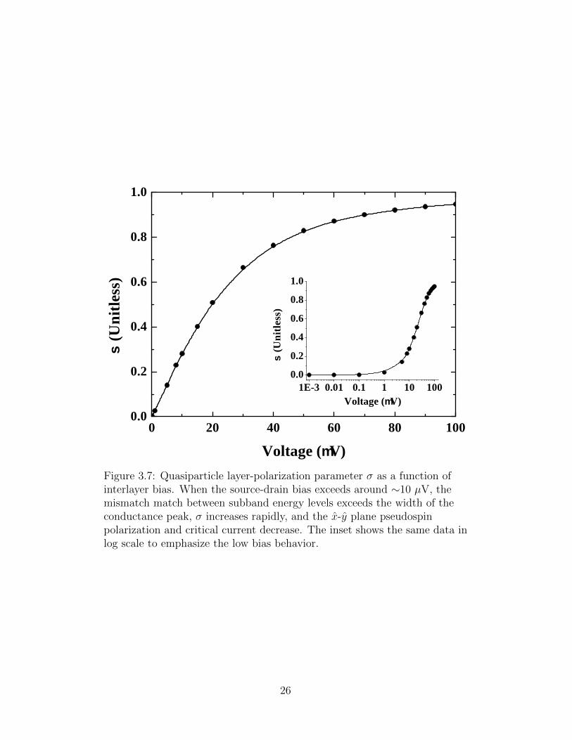
polarized in the z direction. We illustrate this behavior in Figure 3.7 by
plotting
σ = ∆z/√
∆2z + ∆2
c (3.22)
vs. bias voltage, where ∆z is z directional pseudospin field and ∆c is a con-
stant beyond which charge imbalance of the system becomes significant [65].
The magnitude of the x − y direction pseudospin polarization consequently
decreases. In our simulations the critical current decreases more rapidly
than the current in this regime. As shown in Figure 3.5, φps approaches π/2
(mx → 0) at the largest bias voltages (∼100 µV) for which we are able to ob-
tain a steady state solution of the non-equilibrium self-consistent equations.
20
3.5 Figures
Figure 3.1: (a) Device cross section in x− z direction. For the clean system(Chapter 3), interlayer bias configuration of VTR = VTL = 0,VBR = VBL = VINT is used, whereas VTL = VTR = VBR = 0, VBR = VINTconfiguration is used for the disordered system (Chapter 4). (b) A flowchart of the simulation procedure.
Figure 3.2: Schematic of the Fermi surfaces of the bilayer system containingpopulations of symmetric and antisymmetric states separated in energy bya single-particle tunneling term, ∆SAS = 2t.
21
1 2 3 4 50
1
2
3
4
5
Co
nduct
ance
(2e2 /h)
S ( u n i t l e s s )
1 2 3 4 5 6048
1 21 62 0
S ( U n i t l e s s )
Cond
uctan
ce (N
orm.)
Figure 3.3: Plot of the height of the interlayer conductance as a function ofthe interlayer exchange enhancement S at interlayer bias VINT = 10 nV. Inthe inset, we plot of the height of the interlayer conductance normalized tothe non-interacting conductance (S = 1) as a function of S with the samex-axis. We clearly see that the height of the interlayer conductance followsan S2 dependence. The single-particle tunneling amplitude t = ∆SAS/2 =1 µeV.
22
- 1 0 0 - 7 5 - 5 0 - 2 5 0 2 5 5 0 7 5 1 0 0- 1 0 00
1 0 02 0 03 0 04 0 05 0 06 0 0
S = 1 S = 2 S = 4
dI/dV
(mS)
V o l t a g e ( m V )
- 1 0 0 - 5 0 0 5 0 1 0 0- 6- 4- 20246
I (nA
)
V o l t a g e ( m V )
Figure 3.4: Plot of the differential conductance of the bilayer system atS = 4 (orange triangle), S = 2 (blue circle), and S = 1 (openedrectangular) as a function of interlayer bias VINT at 0 K. In the inset, thesame plot in negative interlayer bias with same y-axis is plotted with x-axisin log scale. In a small bias window, almost constant interlayertransconductance is observed. After the interlayer bias reachesVINT ≈ 10 µV, an abrupt drop in transconductance can be seen in theinteracting electron cases of S = 2, 4. We plot the current vs. bias voltagefor each enhancement factor in the inset.
23
0 . 0 0 . 4 0 . 8 1 . 2 1 . 6 2 . 00 . 0
0 . 2
0 . 4
0 . 6
0 . 8
1 . 0
m/m 0 (U
nitles
s)
I n t e r l a y e r c u r r e n t ( n A )
< m x > / m 0 < m y > / m 0 < m z > / m 0 | m x y | / m 0
Figure 3.5: Pseudospin polarization vs. current. The quantities areexpressed in units of the value of mx at zero bias (m0). The points in thisplot correspond to the same points that appear in the inset of current vs.bias voltage in Figure 3.4. For zero-current, the pseudospin is in thex-direction and has a value close to m0 = ν0St. mx decreasesmonotonically, mz increases monotonically, and my increasesnearly-monotonically before saturating at the largest field values. Thearrow in the plot indicates the direction in which a bias voltage increases.
24
0 2 0 4 0 6 0 8 0 1 0 00 . 0
0 . 2
0 . 4
0 . 6
0 . 8
1 . 0
m/m 0 (U
nitles
s)
V o l t a g e ( m V )
< m x > / m 0 < m y > / m 0 < m z > / m 0 | m x y | / m 0
0 2 5 5 0 7 5 1 0 0048
1 21 62 02 4
m/m 0(U
nitles
s)
V o l t a g e ( m V )
Figure 3.6: Pseudospin polarization vs. bias voltage. The quantities areexpressed in units of the value of mx at zero bias (m0). The inset of thisplot clearly shows that mz increases monotonically with bias voltage whicheventually causes the current to decrease. The |mxy| decreases only slowlywith bias voltage because of the compensating effects of pseudospinrotation toward the z-direction and an increase in the overall pseudospinpolarization. There is no steady state solution to the self-consistenttransport equations beyond the largest bias voltage plotted here, becausethe pseudospin orientation φps has reached π/2.
25
0 2 0 4 0 6 0 8 0 1 0 00 . 0
0 . 2
0 . 4
0 . 6
0 . 8
1 . 0
s (Un
itless)
V o l t a g e ( m V )
1 E - 3 0 . 0 1 0 . 1 1 1 0 1 0 00 . 00 . 20 . 40 . 60 . 81 . 0
V o l t a g e ( m V )
s (Un
itless)
Figure 3.7: Quasiparticle layer-polarization parameter σ as a function ofinterlayer bias. When the source-drain bias exceeds around ∼10 µV, themismatch match between subband energy levels exceeds the width of theconductance peak, σ increases rapidly, and the x-y plane pseudospinpolarization and critical current decrease. The inset shows the same data inlog scale to emphasize the low bias behavior.
26
CHAPTER 4
THE EFFECT OF DISORDER IN THESEMICONDUCTOR BILAYER SYSTEM
In this chapter, the effects of disorder on the interlayer transport properties
are evaluated by performing self-consistent quantum transport calculations.
4.1 Modeling of Disorder
We are interested in electron transport of GaAs/AlGaAs heterojunction sys-
tem with impurities. In this thesis, we are particularly interested in the
effects of ionized impurity and roughness at the interface of heterojunction
in GaAs/AlGaAs system [66, 67, 68, 69]. The impurities are assumed to
be highly screened in 2DEG and, as a result, the impurity potential can be
described as a δ-function
U(r) = u∑l
δ(r − rl), (4.1)
where rl is position of lth impurity with amplitude u [66, 67]. If the impurity
is a major scattering source, a mean free path Λ is expressed within the Born
approximation as [67]
Λ =~3vF
ni〈U2〉m∗(4.2)
where vF is Fermi velocity, ni is the impurity number per unit area and
m∗ is an effective mass. Within a lattice model with a lattice constant a,
random disorders can be inserted into the system Hamiltonian by adding
a uniform distribution having a window of W to the diagonal term in the
Hamiltonian. Then, the on-site energy in the disordered system satisfies the
inequality −W/2 ≤ εi − ε0 ≤ W/2, where εi(0) is an on-site energy of the
system with (without) disorder [69]. As a result, the lattice model containing
27
high concentration of δ-function impurities satisfies the relation
ni〈U2〉 = a2〈(εi − ε0)2〉 =a2W
12. (4.3)
From Eqs. (4.2) and (4.3), we can get a width of uniform distribution W as
a function of a mean free path Λ [68, 69]
W
EF=
(6λ3
F
π3a2Λ
)1/2
, (4.4)
where EF , λF are Fermi energy and Fermi wavelength, respectively. Con-
sequently, the impurity level is now characterized by a mean free path, Λ.
At a given MFP, the random disorder potential changes the on-site potential
landscape of the device according to Eq. (4.4), and variations in the poten-
tial landscape act as rigid scatterers. The effect of those scatterers on the
electron propagation is evaluated in the limit of coherent transport, as there
is no phase-breaking mechanism included (e.g. phonon scattering) [51, 50].
Therefore, the current may be calculated by the Landauer formula as has
been done in previous studies on doping and surface roughness in Si [70] and
bulk and edge disorder in graphene nanoribbons [71].
4.2 Simulation Details
Now we consider the system which is comprised of two 16 nm deep GaAs
quantum wells separated by a 2 nm Al0.9Ga0.1As barrier. The gates on the
top and bottom are isolated from their respective quantum well with 60 nm
thick top and bottom Al0.9Ga0.1As barriers. The structure of the system
is identical to the system we considered in Chapter 3 which is illustrated
in Figure 3.1a, but now we have two-dimensional channels instead of one-
dimensional decoupled channels in Chapter 3. We use the tunneling bias
configuration (VTL = VTR = VBL = 0, VBR = VINT ) in which electrons are
injected into the bottom right contact and are extracted from the top left
contact. The length and width of the system are each 1.2 µm and we assume
that each 2DEG contains an electron concentration of 3 × 1010 cm−2. The
system temperature for all of our simulations is set to the zero temperature
limit or T = 0 K.
28
The calculation strategy follows a standard self-consistent field procedure
as shown in Figure 3.1b. We can evaluate the mean-field quasiparticle Hamil-
tonian with the NEGF formalism coupled with a 3D Poisson equation. The
effective interlayer interaction, ∆ in Eq. (3.2), is also updated during the
loop and the loop proceeds until a desired level of self-consistency is achieved.
When the MPF is larger than the system length, there is no significant modi-
fication to the interlayer transport. Thus, we only focus on the MFP compa-
rable to or smaller than the device size. When the MFP is comparable to the
device size, however, the many-body contribution to ∆ shows local fluctua-
tions around the region where the on-site potential is significantly modified.
As these numerical fluctuations are not critical for global observables and
depend on the particular disorder configurations, the data obtained from the
simulation are averaged over six different disorder configurations in order to
mitigate the numerical fluctuations.
4.3 Results and Discussions
In Figure 4.1, we analyze the I − V characteristics of the disordered system
sweeping the interlayer bias up to VINT = 100 µV. We now introduce impu-
rities into the system corresponding to three different MFPs of Λ = 1.2, 0.6,
and 0.3 µm. The range of MFPs we consider here adds a significant per-
turbation to the on-site energy of 10 ∼ 20% of the self-consistent Hartree
potential. In Figure 4.1a, we plot the current flowing from the bottom right
contact (BR) to the top left contact (TL) and immediately see the effects of
disorder. By comparing the interacting (S = 2) and non-interacting (S = 1)
systems, we notice that the interacting system has a uniform current en-
hancement over the non-interacting case over all interlayer voltages. How-
ever, when disorder corresponding to a MFP commensurate with the system
size is introduced, we see that the interlayer current is increased at low VINT .
This is a consequence of local regions of stronger interlayer interactions set
up by disorder-induced localization. As VINT is increased, the interlayer en-
hancement quickly disappears and leaves only a small exchange enhancement
over the non-interacting case. As the MFP is further decreased, we see that
the trend of decreased interlayer exchange enhancement continues as the per-
turbations to the carriers via the disorder potential are now large enough to
29
energetically separate the two layers, leaving only weak single-particle inter-
layer interactions. A separate way of visualizing the effects of disorder is
via Figure 4.1b where we plot the current injected from the bottom right
(BR) contact and extracted from the top right contact (TR). Here, we would
expect the interlayer current to be close to zero as we see for the S = 1 and
S = 2 cases without disorder. However, when disorder localizes the electron
states in the bottom layer, interlayer tunneling is locally enhanced, leading to
increased interlayer transmission near the injection contact. Beyond locally
enhanced transmission, the presence of disorder in the top layer perturbs the
electron states leading to backscattering of injected states. The overall effect
is an increasing current from BR to TR as disorder increases.
A crucial component to understanding the interlayer dynamics in the pres-
ence of materials disorder is the critical current (Ic), or amount of interlayer
current the system can sustain by simply altering the interlayer phase. As
we have not passed a phase boundary, we do not expect large differences in
interlayer currents between before and after the critical current. The critical
current of the clean system from the simulation is Icleanc = 0.89 nA, which
is smaller than the predicted critical current [72] of Ianalc = 1.44 nA. This
discrepancy can be understood by considering the charge imbalance of two
layers, which is addressed in Chapter 3.4. As the bottom layer is biased, the
charge imbalance of two layers builds up the electrostatic potential difference
between two layers. When the charge imbalance between two layers is suffi-
ciently large, two nested Fermi surfaces are separated and the system is in an
off-resonant condition. As a result, the interlayer current is decreased before
the system reaches the critical current. We calculate a critical current for
each disorder configuration and MFP and find that I1.2µmc = 0.67± 0.02 nA,
I0.6µmc = 0.72±0.09 nA, and I0.3µm
c = 0.74±0.07 nA, all of which are smaller
than the disorder-free case. We find the critical current saturates with in-
creasing disorder but this is simply because the exchange enhancement has
been lost and the system responds as if it is non-interacting for MFPs shorter
than the system dimensions.
The effect of disorder can be quantitatively analyzed by probing the inter-
layer conductance. With the presence of the scattering source in the system,
the spectral function of 2DEG has Lorentzian form within the Born approxi-
mation [42] and, therefore, the tunneling conductance also follows Lorentzian
30
shape as [59]
G =IINTVINT
= G0Γ2
Γ2 + (∆EF + eVINT )2, (4.5)
where G0 is a conductance constant and VINT is an interlayer bias. ∆EF is
the electrostatic potential difference between the top and bottom layer and
∆EF = 0 at VINT = 0 when two layers are well balanced. The tunneling
linewidth Γ is the half width at half maximum in a G vs. VINT plot and
satisfies the following relation
Γ =~τ, (4.6)
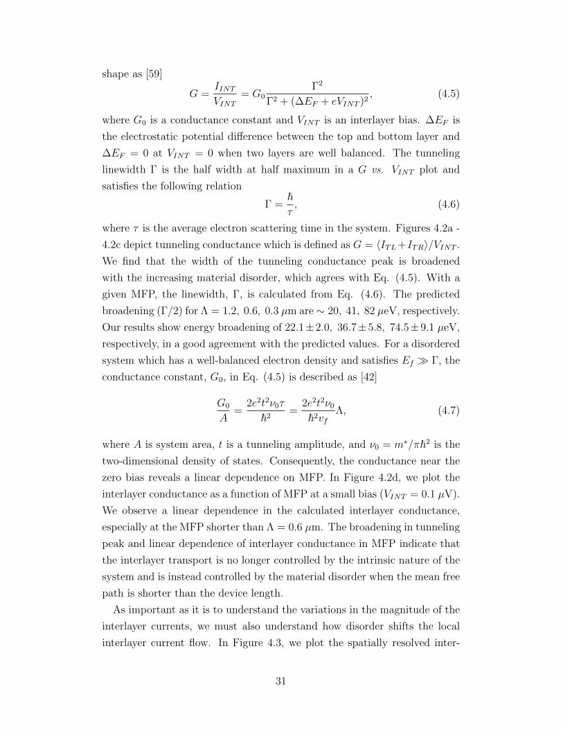
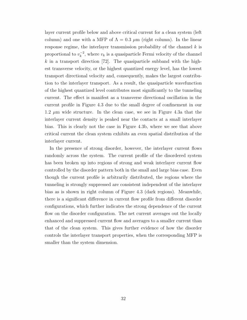
where τ is the average electron scattering time in the system. Figures 4.2a -
4.2c depict tunneling conductance which is defined as G = 〈ITL+ITR〉/VINT .
We find that the width of the tunneling conductance peak is broadened
with the increasing material disorder, which agrees with Eq. (4.5). With a
given MFP, the linewidth, Γ, is calculated from Eq. (4.6). The predicted
broadening (Γ/2) for Λ = 1.2, 0.6, 0.3 µm are∼ 20, 41, 82 µeV, respectively.
Our results show energy broadening of 22.1±2.0, 36.7±5.8, 74.5±9.1 µeV,
respectively, in a good agreement with the predicted values. For a disordered
system which has a well-balanced electron density and satisfies Ef � Γ, the
conductance constant, G0, in Eq. (4.5) is described as [42]
G0
A=
2e2t2ν0τ
~2=
2e2t2ν0
~2vfΛ, (4.7)
where A is system area, t is a tunneling amplitude, and ν0 = m∗/π~2 is the
two-dimensional density of states. Consequently, the conductance near the
zero bias reveals a linear dependence on MFP. In Figure 4.2d, we plot the
interlayer conductance as a function of MFP at a small bias (VINT = 0.1 µV).
We observe a linear dependence in the calculated interlayer conductance,
especially at the MFP shorter than Λ = 0.6 µm. The broadening in tunneling
peak and linear dependence of interlayer conductance in MFP indicate that
the interlayer transport is no longer controlled by the intrinsic nature of the
system and is instead controlled by the material disorder when the mean free
path is shorter than the device length.
As important as it is to understand the variations in the magnitude of the
interlayer currents, we must also understand how disorder shifts the local
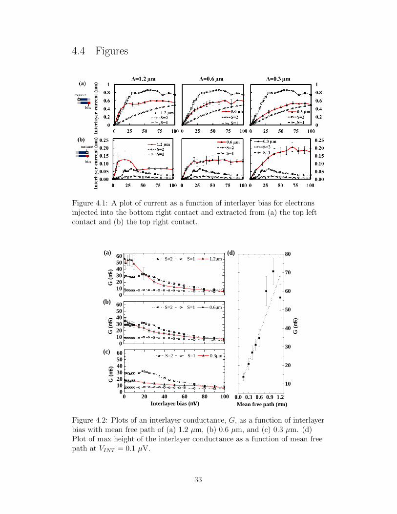
interlayer current flow. In Figure 4.3, we plot the spatially resolved inter-
31
layer current profile below and above critical current for a clean system (left
column) and one with a MFP of Λ = 0.3 µm (right column). In the linear
response regime, the interlayer transmission probability of the channel k is
proportional to v−2k , where vk is a quasiparticle Fermi velocity of the channel
k in a transport direction [72]. The quasiparticle subband with the high-
est transverse velocity, or the highest quantized energy level, has the lowest
transport directional velocity and, consequently, makes the largest contribu-
tion to the interlayer transport. As a result, the quasiparticle wavefunction
of the highest quantized level contributes most significantly to the tunneling
current. The effect is manifest as a transverse directional oscillation in the
current profile in Figure 4.3 due to the small degree of confinement in our
1.2 µm wide structure. In the clean case, we see in Figure 4.3a that the
interlayer current density is peaked near the contacts at a small interlayer
bias. This is clearly not the case in Figure 4.3b, where we see that above
critical current the clean system exhibits an even spatial distribution of the
interlayer current.
In the presence of strong disorder, however, the interlayer current flows
randomly across the system. The current profile of the disordered system
has been broken up into regions of strong and weak interlayer current flow
controlled by the disorder pattern both in the small and large bias case. Even
though the current profile is arbitrarily distributed, the regions where the
tunneling is strongly suppressed are consistent independent of the interlayer
bias as is shown in right column of Figure 4.3 (dark regions). Meanwhile,
there is a significant difference in current flow profile from different disorder
configurations, which further indicates the strong dependence of the current
flow on the disorder configuration. The net current averages out the locally
enhanced and suppressed current flow and averages to a smaller current than
that of the clean system. This gives further evidence of how the disorder
controls the interlayer transport properties, when the corresponding MFP is
smaller than the system dimension.
32
4.4 Figures
Figure 4.1: A plot of current as a function of interlayer bias for electronsinjected into the bottom right contact and extracted from (a) the top leftcontact and (b) the top right contact.
0 2 0 4 0 6 0 8 0 1 0 001 02 03 04 05 06 0
I n t e r l a y e r b i a s ( m V )
G (m
S)
S = 2 S = 1 0 . 3 µm0
1 02 03 04 05 06 0
G (m
S)
S = 2 S = 1 0 . 6 µm0
1 02 03 04 05 06 0
G (m
S)
S = 2 S = 1 1 . 2 µm
( c )
( b )
0 . 0 0 . 3 0 . 6 0 . 9 1 . 21 0
2 0
3 0
4 0
5 0
6 0
7 0
8 0
M e a n f r e e p a t h ( m m )
G (m
S)
( d )( a )
Figure 4.2: Plots of an interlayer conductance, G, as a function of interlayerbias with mean free path of (a) 1.2 µm, (b) 0.6 µm, and (c) 0.3 µm. (d)Plot of max height of the interlayer conductance as a function of mean freepath at VINT = 0.1 µV.
33
Widt
h (mm
)
0 . 0
0 . 4
0 . 8
1 . 2 0 . 0 0 . 4 0 . 8 1 . 20 . 0 00 . 0 40 . 0 80 . 1 2
0 . 0 0 . 4 0 . 8 1 . 2
- 0 . 1
0 . 0
0 . 1
0 . 2
0 . 30 . 00 . 10 . 2
0 . 0
0 . 4
0 . 8
1 . 2 0 . 0 0 . 4 0 . 8 1 . 20 . 00 . 10 . 20 . 3
0 . 0 0 . 4 0 . 8 1 . 2
- 0 . 5- 0 . 20 . 10 . 40 . 71 . 0
0 . 00 . 30 . 6
L e n g t h ( m m )L e n g t h ( m m )
Widt
h (mm
)L = 0 . 3 m mC l e a n
( b )
( a )I(p
A)I(p
A)W
idth (
mm)
Figure 4.3: A plot of spatially resolved current as a function of device widthand length at (a) VINT = 10 µV and (b) VINT = 80 µV in units of pA foran assumed enhancement factor of S = 2. The current profile of the cleansystem (disordered system of Λ = 0.3 µm) is presented in top and bottomleft (top and bottom right) panels of this figure. Above eachtwo-dimensional plot, there is a current profile taken in the middle of thesystem indicated as a white dashed line.
34
CHAPTER 5
CONCLUSION
For a balanced double quantum well system, the equilibrium electronic eigen-
states have symmetric or antisymmetric bilayer wavefunctions. When the
interlayer exchange interaction of the bilayer system is described using a
pseudospin language, the difference between symmetric and antisymmetric
populations corresponds to a x-direction pseudospin polarization. When the
bilayer system is connected to reservoirs that drive current between layers,
it is easy to show that the non-equilibrium pseudospin polarization must tilt
toward the y-direction. The total current that flows between layers is in
fact simply related to the total y-direction pseudospin polarization. These
properties suggest the possibility that electron-electron interactions can qual-
itatively alter interlayer transport under some circumstances. In equilibrium
interactions enhance the quasiparticle inter-layer tunneling amplitude, but
not the total current that can be carried between layers for a given y-direction
pseudospin polarization. If the inter-layer quasiparticle current can be driven
to a value that is larger than can be supported by the inter-layer tunneling
amplitude, the self-consistent equations for the transport steady state have
no solution and time-dependent current response is expected. This effect
has not yet been observed, but is partially analogous to spin-transfer-torque
oscillators in circuits containing magnetic metals. We have demonstrated by
explicit calculation for a model bilayer system that it is in principle possible
to induce this dynamic instability in semiconductor bilayers.
The current-voltage relationship in semiconductor bilayers is character-
ized by a sharp peak in dI/dV at small bias voltages, followed by a regime of
negative differential conductance at larger bias voltages. In our simulations
the pseudospin instability occurs in the regime of negative differential con-
ductance where dynamic responses might also occur simply due to normal
electrical instabilities. It should be possible to distinguish these two effects
experimentally, by varying the circuit resistance that is in series with the
35
bilayer system.
In addition, we have shown that the exchange-enhanced interlayer trans-
port properties in semiconductor bilayers are very sensitive to the strength
and location of material disorder. We find that as soon as the MFP of the
electrons becomes commensurate with the spatial system dimensions, the
disorder controls the interlayer transport properties and reduces the inter-
acting electron system to a non-interacting one. These findings demonstrate
that to observe pseudospin instability and interaction driven interlayer en-
hancement experimentally, one requires systems with MFPs greater than the
system spatial dimensions.
36
REFERENCES
[1] A. B. Fowler, F. F. Fang, W. E. Howard, and P. J. Stiles, “Magneto-oscillatory conductance in silicon surfaces,” Phys. Rev. Lett., vol. 16, pp.901–903, May 1966.
[2] D. C. Tsui, “Observation of surface bound state and two-dimensionalenergy band by electron tunneling,” Phys. Rev. Lett., vol. 24, pp. 303–306, Feb 1970.
[3] R. Dingle, H. L. Stormer, A. C. Gossard, and W. Wiegmann, “Electronmobilities in modulation-doped semiconductor heterojunction superlat-tices,” Applied Physics Letters, vol. 33, no. 7, pp. 665–667, 1978.
[4] E. F. Schubert and K. Ploog, “The δ-doped field-effect transistor,”Japanese Journal of Applied Physics, vol. 24, no. 8, part 2, pp. L608–L610, 1985.
[5] V. Umansky, R. de Picciotto, and M. Heiblum, “Extremely high-mobility two dimensional electron gas: Evaluation of scattering mecha-nisms,” Applied Physics Letters, vol. 71, no. 5, pp. 683–685, 1997.
[6] H. Manoharan, “New particles and phases in reduced-dimensional sys-tems,” Ph.D. dissertation, Princeton University, Princeton, NJ, 1998.
[7] E. H. Rezayi and F. D. M. Haldane, “Lowest-order Landau-level mixingcorrections for 4 ≥ ν > 2 quantum Hall effect,” Phys. Rev. B, vol. 42,pp. 4532–4536, Sep 1990.
[8] D. Yoshioka and A. H. Macdonald, “Double quantum well electron-holesystems in strong magnetic fields,” Journal of the Physical Society ofJapan, vol. 59, no. 12, pp. 4211–4214, 1990.
[9] J. P. Eisenstein and A. H. MacDonald, “Bose-Einstein condensation ofexcitons in bilayer electron systems,” Nature, vol. 432, p. 691, Dec 2004.
[10] K. Moon, H. Mori, K. Yang, S. M. Girvin, A. H. MacDonald, L. Zheng,D. Yoshioka, and S.-C. Zhang, “Spontaneous interlayer coherence indouble-layer quantum Hall systems: Charged vortices and Kosterlitz-Thouless phase transitions,” Phys. Rev. B, vol. 51, no. 8, pp. 5138–5170,Feb 1995.
37
[11] I. B. Spielman, J. P. Eisenstein, L. N. Pfeiffer, and K. W. West, “Reso-nantly enhanced tunneling in a double layer quantum Hall ferromagnet,”Phys. Rev. Lett., vol. 84, no. 25, pp. 5808–5811, Jun 2000.
[12] M. Kellogg, I. B. Spielman, J. P. Eisenstein, L. N. Pfeiffer, and K. W.West, “Observation of quantized Hall drag in a strongly correlated bi-layer electron system,” Phys. Rev. Lett., vol. 88, no. 12, p. 126804, Mar2002.
[13] Y. Yoon, L. Tiemann, S. Schmult, W. Dietsche, K. von Klitzing, andW. Wegscheider, “Interlayer tunneling in counterflow experiments onthe excitonic condensate in quantum Hall bilayers,” Phys. Rev. Lett.,vol. 104, p. 116802, Mar 2010.
[14] L. Tiemann, Y. Yoon, W. Dietsche, K. von Klitzing, and W. Wegschei-der, “Dominant parameters for the critical tunneling current in bilayerexciton condensates,” Phys. Rev. B, vol. 80, no. 16, p. 165120, Oct 2009.
[15] S. Datta, “Nanoscale device modeling: The Green’s function method,”Superlattices and Microstructures, vol. 28, no. 4, pp. 253 – 278, 2000.
[16] R. Shankar, “Renormalization-group approach to interacting fermions,”Rev. Mod. Phys., vol. 66, no. 1, pp. 129–192, Jan 1994.
[17] D. Pines and P. Nozieres, The Theory of Quantum Liquid. Addison-Wesley, New York, 1966.
[18] G. F. Giuliani and G. Vignale, Quantum Theory of the Electron Liquid.Cambridge University Press, Cambridge, 2005.
[19] C. A. Ullrich and G. Vignale, “Time-dependent current-density-functional theory for the linear response of weakly disordered systems,”Phys. Rev. B, vol. 65, no. 24, p. 245102, May 2002.
[20] M. Di Ventra and N. D. Lang, “Transport in nanoscale conductors fromfirst principles,” Phys. Rev. B, vol. 65, no. 4, p. 045402, Dec 2001.
[21] M. J. Gilbert and D. K. Ferry, “Efficient quantum three-dimensionalmodeling of fully depleted ballistic silicon-on-insulator metal-oxide-semiconductor field-effect-transistors,” Journal of Applied Physics,vol. 95, no. 12, pp. 7954–7960, 2004.
[22] M. J. Gilbert, R. Akis, and D. K. Ferry, “Phonon-assisted ballistic todiffusive crossover in silicon nanowire transistors,” Journal of AppliedPhysics, vol. 98, no. 9, p. 094303, 2005.
38
[23] J. Wang, E. Polizzi, and M. Lundstrom, “A three-dimensional quantumsimulation of silicon nanowire transistors with the effective-mass ap-proximation,” Journal of Applied Physics, vol. 96, no. 4, pp. 2192–2203,2004.
[24] N. Sergueev, A. A. Demkov, and H. Guo, “Inelastic resonant tunnelingin C60 molecular junctions,” Phys. Rev. B, vol. 75, no. 23, p. 233418,Jun 2007.
[25] J. Wu, B. Wang, J. Wang, and H. Guo, “Giant enhancement of dynamicconductance in molecular devices,” Phys. Rev. B, vol. 72, no. 19, p.195324, Nov 2005.
[26] D. Waldron, P. Haney, B. Larade, A. MacDonald, and H. Guo, “Nonlin-ear spin current and magnetoresistance of molecular tunnel junctions,”Phys. Rev. Lett., vol. 96, no. 16, p. 166804, Apr 2006.
[27] C. Toher and S. Sanvito, “Efficient atomic self-interaction correc-tion scheme for nonequilibrium quantum transport,” Phys. Rev. Lett.,vol. 99, no. 5, p. 056801, Jul 2007.
[28] A. R. Rocha, V. M. Garcia-suarez, S. W. Bailey, C. J. Lambert, J. Fer-rer, and S. Sanvito, “Towards molecular spintronics,” Nature Materials,vol. 4, p. 335, Mar 2005.
[29] A. S. Nunez and A. H. MacDonald, “Theory of spin transfer phenomenain magnetic metals and semiconductors,” Solid State Communications,vol. 139, no. 1, pp. 31 – 34, 2006.
[30] P. Haney, R. Duine, A. Nunez, and A. MacDonald, “Current-inducedtorques in magnetic metals: Beyond spin-transfer,” Journal of Mag-netism and Magnetic Materials, vol. 320, no. 7, pp. 1300 – 1311, 2008.
[31] P. M. Haney, D. Waldron, R. A. Duine, A. S. Nunez, H. Guo, and A. H.MacDonald, “Current-induced order parameter dynamics: Microscopictheory applied to Co/Cu/Co spin valves,” Phys. Rev. B, vol. 76, no. 2,p. 024404, Jul 2007.
[32] W. H. Rippard, M. R. Pufall, and S. E. Russek, “Comparison of fre-quency, linewidth, and output power in measurements of spin-transfernanocontact oscillators,” Phys. Rev. B, vol. 74, no. 22, p. 224409, Dec2006.
[33] E. Rossi, O. G. Heinonen, and A. H. MacDonald, “Dynamics of mag-netization coupled to a thermal bath of elastic modes,” Phys. Rev. B,vol. 72, no. 17, p. 174412, Nov 2005.
39
[34] X. G. Wen and A. Zee, “Neutral superfluid modes and “magnetic”monopoles in multilayered quantum Hall systems,” Phys. Rev. Lett.,vol. 69, no. 12, pp. 1811–1814, Sep 1992.
[35] O. Gunawan, Y. P. Shkolnikov, E. P. D. Poortere, E. Tutuc, andM. Shayegan, “Ballistic electron transport in AlAs quantum wells,”Phys. Rev. Lett., vol. 93, no. 24, p. 246603, Dec 2004.
[36] R. D. Wiersma, J. G. S. Lok, S. Kraus, W. Dietsche, K. von Klitzing,D. Schuh, M. Bichler, H.-P. Tranitz, and W. Wegscheider, “Activatedtransport in the separate layers that form the νT = 1 exciton conden-sate,” Phys. Rev. Lett., vol. 93, no. 26, p. 266805, Dec 2004.
[37] A. H. MacDonald, “Superfluid properties of double-layer quantum Hallferromagnets,” Physica B: Condensed Matter, vol. 298, no. 1-4, pp. 129– 134, 2001.
[38] T. Jungwirth and A. H. MacDonald, “Resistance spikes and domain wallloops in Ising quantum Hall ferromagnets,” Phys. Rev. Lett., vol. 87,no. 21, p. 216801, Oct 2001.
[39] S. Misra, N. C. Bishop, E. Tutuc, and M. Shayegan, “Tunneling betweendilute GaAs hole layers,” Phys. Rev. B, vol. 77, no. 16, p. 161301, Apr2008.
[40] J. P. Eisenstein, T. J. Gramila, L. N. Pfeiffer, and K. W. West, “Probinga two-dimensional Fermi surface by tunneling,” Phys. Rev. B, vol. 44,no. 12, pp. 6511–6514, Sep 1991.
[41] J. P. Eisenstein, L. N. Pfeiffer, and K. W. West, “Field-induced resonanttunneling between parallel two-dimensional electron systems,” AppliedPhysics Letters, vol. 58, no. 14, pp. 1497–1499, 1991.
[42] L. Zheng and A. H. MacDonald, “Tunneling conductance between par-allel two-dimensional electron systems,” Phys. Rev. B, vol. 47, no. 16,pp. 10 619–10 624, Apr 1993.
[43] J.-J. Su and A. H. MacDonald, “How to make a bilayer exciton conden-sate flow,” Nat. Phys., vol. 4, no. 10, p. 799, Aug 2008.
[44] A. H. MacDonald, “Staging transitions in multiple-quantum-well sys-tems,” Phys. Rev. B, vol. 37, no. 9, pp. 4792–4794, Mar 1988.
[45] P. P. Ruden and Z. Wu, “Exchange effect in coupled two-dimensionalelectron gas systems,” Applied Physics Letters, vol. 59, no. 17, pp. 2165–2167, 1991.
40
[46] G. Senatore and S. D. Palo, “Correlation effects in low dimensionalelectron systems: The electron-hole bilayer,” Contributions to PlasmaPhysics, vol. 43, no. 5-6, pp. 363–368, 2003.
[47] A. Stern, S. D. Sarma, M. P. A. Fisher, and S. M. Girvin, “Dissipation-less transport in low-density bilayer systems,” Phys. Rev. Lett., vol. 84,no. 1, pp. 139–142, Jan 2000.
[48] L. Swierkowski and A. H. MacDonald, “Transverse pseudospin suscepti-bility and tunneling parameters of double-layer electron-gas systems ,”Phys. Rev. B, vol. 55, no. 24, pp. R16 017–R16 020, Jun 1997.
[49] L. Geppert, “Quantum transistors: Toward nanoelectronics,” Spectrum,IEEE, vol. 37, no. 9, pp. 46 –51, sep 2000.
[50] S. Datta, Electronic Transport in Mesoscopic Systems. London: Cam-bridge University Press.
[51] S. Datta, Quantum Transport: Atom to Transistor. London: Cam-bridge University Press.
[52] M. J. Gilbert, “Finite-temperature pseudospin torque effect in graphenebilayers,” Phys. Rev. B, vol. 82, no. 16, p. 165408, Oct 2010.
[53] A. S. Nunez and A. H. MacDonald, “Theory of spin transfer phenomenain magnetic metals and semiconductors,” Solid State Communications,vol. 139, no. 1, pp. 31 – 34, 2006.
[54] K. Park and S. Das Sarma, “Coherent tunneling in exciton condensatesof bilayer quantum Hall systems,” Phys. Rev. B, vol. 74, no. 3, p. 035338,Jul 2006.
[55] R. Venugopal, Z. Ren, S. Datta, M. S. Lundstrom, and D. Jovanovic,“Simulating quantum transport in nanoscale transistors: Real versusmode-space approaches,” Journal of Applied Physics, vol. 92, no. 7, pp.3730–3739, 2002.
[56] H. L. Stone, “Iterative solution of implicit approximations of multidi-mensional partial differential equations,” SIAM Journal on NumericalAnalysis, vol. 5, no. 3, pp. 530–558, 1968.
[57] A. Rahman, J. Guo, S. Datta, and M. Lundstrom, “Theory of ballisticnanotransistors,” Electron Devices, IEEE Transactions on, vol. 50, no. 9,pp. 1853 – 1864, sept. 2003.
[58] D. D. Johnson, “Modified Broyden’s method for accelerating conver-gence in self-consistent calculations,” Phys. Rev. B, vol. 38, no. 18, pp.12 807–12 813, Dec 1988.
41
[59] N. Turner, J. T. Nicholls, E. H. Linfield, K. M. Brown, G. A. C. Jones,and D. A. Ritchie, “Tunneling between parallel two-dimensional electrongases,” Phys. Rev. B, vol. 54, no. 15, pp. 10 614–10 624, Oct 1996.
[60] S. K. Lyo, “Nonlinear interlayer tunneling in a double-electron-layerstructure,” Phys. Rev. B, vol. 61, no. 12, pp. 8316–8325, Mar 2000.
[61] H. Min, R. Bistritzer, J.-J. Su, and A. H. MacDonald, “Room-temperature superfluidity in graphene bilayers,” Phys. Rev. B, vol. 78,no. 12, p. 121401, Sep 2008.
[62] J. A. Seamons, D. R. Tibbetts, J. L. Reno, and M. P. Lilly, “Undopedelectron-hole bilayers in a GaAs/AlGaAs double quantum well,” AppliedPhysics Letters, vol. 90, no. 5, p. 052103, 2007.
[63] C.-H. Zhang and Y. N. Joglekar, “Excitonic condensation of masslessfermions in graphene bilayers,” Phys. Rev. B, vol. 77, no. 23, p. 233405,Jun 2008.
[64] A. V. Balatsky, Y. N. Joglekar, and P. B. Littlewood, “Dipolar superflu-idity in electron-hole bilayer systems,” Phys. Rev. Lett., vol. 93, no. 26,p. 266801, Dec 2004.
[65] J. Bourassa, B. Roostaei, R. Cote, H. A. Fertig, and K. Mullen, “Pseu-dospin vortex-antivortex states with interwoven spin textures in double-layer quantum Hall systems,” Phys. Rev. B, vol. 74, no. 19, p. 195320,Nov 2006.
[66] T. Ando, “Localization in a quantum Hall regime: Mixed short- andlong-range scatterers,” Phys. Rev. B, vol. 40, no. 14, pp. 9965–9968,Nov 1989.
[67] H. Akera and T. Ando, “Theory of the Hall effect in quantum wires:Effects of scattering,” Phys. Rev. B, vol. 41, no. 17, pp. 11 967–11 977,Jun 1990.
[68] T. Ando, “Quantum point contacts in magnetic fields,” Phys. Rev. B,vol. 44, no. 15, pp. 8017–8027, Oct 1991.
[69] T. Ando and H. Tamura, “Conductance fluctuations in quantum wireswith spin-orbit and boundary-roughness scattering,” Phys. Rev. B,vol. 46, no. 4, pp. 2332–2338, Jul 1992.
[70] A. Martinez, J. R. Barker, N. Seoane, A. R. Brown, and A. Asenov,“Dopants and roughness induced resonances in thin Si nanowire transis-tors: A self-consistent NEGF-Poisson study,” Journal of Physics: Con-ference Series, vol. 220, no. 1, p. 012009, 2010.
42
[71] Y. Sui, T. Low, M. Lundstrom, and J. Appenzeller, “Signatures of dis-order in the minimum conductivity of graphene,” Nano Letters, vol. 11,no. 3, pp. 1319–1322, 2011.
[72] Y. Kim, A. H. MacDonald, and M. J. Gilbert, “Pseudospin transfertorques in semiconductor electron bilayers,” Phys. Rev. B, vol. 85, p.165424, Apr 2012.
43

![Critical ideals of graphs - CINVESTAV · G], the determinantal ideals of L(G;X G) are ideals on Z[X G] which we call critical ideals of G. Next we study how the critical ideals encode](https://img.pdfslide.us/doc/110x75/5fa3f5e4efc6f36b113a3fab/critical-ideals-of-graphs-cinvestav-g-the-determinantal-ideals-of-lgx-g-are.jpg)