Embed Size (px)
Citation preview

Copyright
by
Olga Kardonik
2013

The Report Committee for Olga Kardonik
Certifies that this is the approved version of the following report:
A Study of SAR ADC and
Implementation of 10-bit Asynchronous Design
APPROVED BY
SUPERVISING COMMITTEE:
Nan Sun
T R Viswanathan
Supervisor:

A Study of SAR ADC and
Implementation of 10-bit Asynchronous Design
by
Olga Kardonik, Diplom.
Report
Presented to the Faculty of the Graduate School of
The University of Texas at Austin
in Partial Fulfillment
of the Requirements
for the Degree of
Master of Science in Engineering
The University of Texas at Austin
August 2013

Dedicated to my family

v
Acknowledgements
I would like to acknowledge Professor Nan Sun who sparked my interest in
mixed-signal integrated circuits and data converter design. His teaching has helped me to
make this work a possibility. His encouragement kept me on track and supported
throughout the work. I also would like to thank him for making his classes as ones of the
best in the graduate school.
I am thankful to Professor T. R. Viswanathan for being report’s reader. Only
once I had an opportunity to listen to his lecture, and I was absolutely inspired by his
passionate affection for teaching and engineering.
I would like to thank Yeonam Yoon and Arindam Sanyal, PhD students in ECE
department, for their help regardless busy schedule. I learned a lot from them.

vi
Abstract
A Study of SAR ADC and
Implementation of 10-bit Asynchronous Design
Olga Kardonik, M.S.E.
The University of Texas at Austin, 2013
Supervisor: Nan Sun
Successive Approximation Register (SAR) Analog-to-Digital Converters (ADCs)
achieve low power consumption due to its simple architecture based on dominant digital
content. SAR ADCs do not require an op-amp, so they are advantageous in CMOS
technology scaling. The architecture is often the best choice for battery-powered or
mobile applications which need medium resolution (8-12 bits), medium speed (10 - 100
MS/s) and require low-power consumption and small form factor. This work studies the
architecture in depth, highlighting its main constraints and tradeoffs involving into SAR
ADC design. The work researches asynchronous operation of SAR logic and investigates
the latest trends for ADC’s analog components – comparator and DAC. 10-bit
asynchronous SAR ADC is implemented in CMOS 0.18 µm. Design’s noise and power
are presented as a breakdown among components.

vii
Table of Contents
List of Tables ......................................................................................................... ix
List of Figures ..........................................................................................................x
Chapter 1: SAR ADC Architecture ..........................................................................1
1.1 Motivations ...............................................................................................1
1.2 Top-Level Operation .................................................................................2
1.3 SAR Energy ..............................................................................................4
1.4 SAR Algorithm – Single-Ended ...............................................................5
1.5 SAR Algorithm – Differential ..................................................................7
Chapter 2: Capacitive DAC ..................................................................................11
2.1 Nonlinearity ............................................................................................11
2.2 Constraints For Switches ........................................................................12
2.3 Bottom Plate Sampling vs. Top Plate Sampling .....................................13
2.4 Trends in Capacitive DAC Design .........................................................15
Chapter 3: Comparator .........................................................................................19
3.1 Metrics ....................................................................................................19
3.2 Dynamic Latched Comparator ................................................................21
3.3 Two-Stage Dynamic Latched Comparator .............................................24
Chapter 4: Successive Approximation Register ....................................................27
4.1 Synchronous SAR Logic.........................................................................27
4.2 Asynchronous SAR Logic ......................................................................29
Chapter 5: Design of a 10-bit asynchronous SAR ADC ........................................34
5.1 DAC ........................................................................................................34
5.2 Comparator .............................................................................................37
5.3 Top-Level ................................................................................................39
5.4 SAR Logic ..............................................................................................40

viii
Chapter 6: Simulations and Results ......................................................................46
6.1 DAC ........................................................................................................46
6.2 Comparator .............................................................................................50
6.3 SAR Logic ..............................................................................................55
6.4 Top-Level and Conclusions ....................................................................57
Bibliography ..........................................................................................................62

ix
List of Tables
Table 5.1: Bottom plate switch operation for asynchronous SAR ADC ...........35
Table 5.2: Sizing of the switches .......................................................................36
Table 5.3: Sizing of comparator transistors .......................................................38
Table 6.1: Transient noise results.......................................................................53
Table 6.3: Power and noise results .....................................................................60

x
List of Figures
Figure 1.1: SAR ADC architecture. ......................................................................2
Figure 1.2: 4-bit SAR ADC operation. ..................................................................3
Figure 1.3: Theoretical SAR energy versus resolution. ........................................4
Figure 1.4: Single-ended capacitive DAC of 3-bit SAR ADC, Vcm = 0. .............5
Figure 1.5: Differential capacitive DAC of 3-bit SAR ADC, sampling phase. ....8
Figure 1.6: Bit3 (MSB) test. ..................................................................................9
Figure 1.7: Bit2 test, assuming bit3 is 1. .............................................................10
Figure 2.1: Model of a poly-poly capacitor. ........................................................14
Figure 2.2: B-bit split capacitor array in [17]. .....................................................16
Figure 2.3: Vcm-based switching for split array in [18]. ....................................17
Figure 2.4: Initial cycle of the switching approach in [19]. ................................18
Figure 2.5: Following cycles of the switching approach in [19]. ........................18
Figure 3.1: Comparator sign and its transfer function. ........................................19
Figure 3.2: Two-stage comparator with offset modeling. ...................................20
Figure 3.3: Kickback noise modeling. .................................................................21
Figure 3.4: Strong-arm sense amplifier. ..............................................................22
Figure 3.5: Dynamic latched comparator. ...........................................................23
Figure 3.6: Double-tail latch-type voltage sense amplifier in [9]. ......................24
Figure 3.7: Two-stage dynamic latched comparator. ..........................................26
Figure 4.1: Synchronous SAR logic to control single-ended DAC.....................27
Figure 4.2: Timing diagram of 3-bit synchronous SAR logic. ............................28
Figure 4.3: Synchronous vs. Asynchronous SAR conversion. ............................29
Figure 4.4: Asynchronous approach for SAR logic in [21].................................30

xi
Figure 4.5: State machine of main control and DAC control. .............................31
Figure 4.6: Implementation of main control and DAC control. ..........................31
Figure 4.7: Asynchronous SAR architecture in [22]. ..........................................32
Figure 4.8: Asynchronous SAR architecture in [24]. ..........................................33
Figure 5.1: Top plate switch. ...............................................................................34
Figure 5.2: Bottom plate switch network for asynchronous SAR ADC. ............35
Figure 5.3: Bottom plate network of Cdummy capacitor. ...................................36
Figure 5.4: Implemented comparator. .................................................................37
Figure 5.5: Top-level of asynchronous 10-bit SAR. ...........................................39
Figure 5.6: CLKC clock generator. .....................................................................41
Figure 5.7: SAR shift register. .............................................................................42
Figure 5.8: SAR code register. ............................................................................42
Figure 5.9: Timing diagram of the asynchronous SAR logic. .............................44
Figure 5.10: D-FF. .................................................................................................45
Figure 5.11: XOR and MUX gates. .......................................................................45
Figure 6.1: DAC simulation in ideal-level environment. ....................................46
Figure 6.2: DAC settling. ....................................................................................47
Figure 6.3: Time instances for DAC transient noise. ..........................................48
Figure 6.4: DAC transient noise for the first 5 time instances. ...........................48
Figure 6.5: DAC transient noise analysis for a time sample. ..............................49
Figure 6.6: Average transient noise of the DAC. ................................................50
Figure 6.7: Test-bench for the comparator validation. ........................................51
Figure 6.8: Comparator performance. .................................................................52
Figure 6.9: Drop due to small input delta. ...........................................................52
Figure 6.10: Transient noise when delta = 600 µV. ..............................................54

xii
Figure 6.11: Transient noise when delta = 300 µV. ..............................................54
Figure 6.12: Transient noise when delta = 200 µV. ..............................................54
Figure 6.13: Transient noise analysis for Dout bits. ..............................................56
Figure 6.14: Average transient noise of the SAR logic. ........................................56
Figure 6.15: Timing of the MSB approximation. ..................................................57
Figure 6.16: 64-point FFT. ....................................................................................58
Figure 6.17: 64-point FFT, DAC only...................................................................59
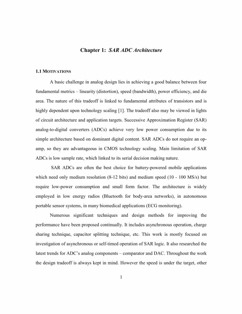
1
Chapter 1: SAR ADC Architecture
1.1 MOTIVATIONS
A basic challenge in analog design lies in achieving a good balance between four
fundamental metrics – linearity (distortion), speed (bandwidth), power efficiency, and die
area. The nature of this tradeoff is linked to fundamental attributes of transistors and is
highly dependent upon technology scaling [1]. The tradeoff also may be viewed in lights
of circuit architecture and application targets. Successive Approximation Register (SAR)
analog-to-digital converters (ADCs) achieve very low power consumption due to its
simple architecture based on dominant digital content. SAR ADCs do not require an op-
amp, so they are advantageous in CMOS technology scaling. Main limitation of SAR
ADCs is low sample rate, which linked to its serial decision making nature.
SAR ADCs are often the best choice for battery-powered mobile applications
which need only medium resolution (8-12 bits) and medium speed (10 - 100 MS/s) but
require low-power consumption and small form factor. The architecture is widely
employed in low energy radios (Bluetooth for body-area networks), in autonomous
portable sensor systems, in many biomedical applications (ECG monitoring).
Numerous significant techniques and design methods for improving the
performance have been proposed continually. It includes asynchronous operation, charge
sharing technique, capacitor splitting technique, etc. This work is mostly focused on
investigation of asynchronous or self-timed operation of SAR logic. It also researched the
latest trends for ADC’s analog components – comparator and DAC. Throughout the work
the design tradeoff is always kept in mind. However the speed is under the target, other

2
metrics may not be sacrificed in significant extent, braking the practical balance and
overall attractiveness of the architecture.
1.2 TOP-LEVEL OPERATION
SAR ADC operates by using a binary search algorithm to converge on the input
signal. The basic architecture is shown on Figure 1.1.
Figure 1.1: SAR ADC architecture.
Analog input voltage, Vin, is held on a Sample/Hold device. To implement the
binary search, N-bit code register in SAR logic block (see chapter 5.1) is first set to
midscale: N’b100…00, where MSB is logic 1. This forces the DAC output ( ) to be
half of the reference voltage ( ). Then the comparator performs a comparison between
Vin and : if Vin is greater than , the comparator output is a logic high and the
MSB of the N-bit code register remains at logic 1; if Vin is less than , the
comparator output is a logic low and the MSB of the register cleared to logic 0. The SAR
logic then moves to the next bit down, forces that bit high, and does another comparison.
N-bit
Dout[N-1:0]
Vref

3
The sequence continues all the way down to LSB. Once this is done, the conversion is
complete and the N-bit digital word is available in the SAR’s code register.
Figure 1.2 shows an example of 4-bit SAR conversion. The final digital code (and
the output from the ADC) is 4’b0101.
Figure 1.2: 4-bit SAR ADC operation.
Many SAR ADCs use a capacitive DAC that provides an inherent Sample/Hold
function. Therefore S/H block shown on figure 1.1 may not be an explicit circuit
anymore. Charge-redistribution DACs based on switched capacitors are prevalent in
nowadays SAR ADCs. The advantage of the switched capacitor DAC is that the accuracy
and linearity is primarily determined by high-accuracy photolithography, which, at some
extends, is able to controls the capacitor plate area, capacitance value as well as
matching. So modern fine-line CMOS processes are ideal for the switched capacitor SAR
ADC, and the cost is therefore low [13].
SAR ADC’s speed is limited by DAC settling time; by comparator, which must
resolve small difference in Vin and within the specified time; and by SAR logic
operation. The overall accuracy and linearity of the SAR ADC is determined primarily by

4
the DAC. Because of the inherent component-matching limitations, SAR ADCs with
more than 12 bits of resolution will often require some form of trimming or calibration to
achieve the necessary linearity. Although it is “process-and-design” dependent,
component matching limits the linearity to about 12 bits in practical DAC designs [14].
1.3 SAR ENERGY
Theoretical energy distribution among SAR ADC components is analyzed in [16]
and shown here in figure 1.3. It shows total SAR energy per conversion along with the
individual components: comparator, DAC array, digital logic.
Figure 1.3: Theoretical SAR energy versus resolution.
At low resolutions the digital energy dominates, and the total energy grows linearly with
number of bits. At some point the comparator begins to dominate with energy growing as
. At high resolutions the growing size and matching requirements of the capacitor
array dominate and the energy grows as (
)
, where α is a coefficient related to DAC

5
capacitance mismatch and equal to ¾ or ½ depending if the mismatch dominated by edge
effect or oxide variation.
1.4 SAR ALGORITHM – SINGLE-ENDED
A capacitive DAC consists of an array of N capacitors with binary weighted
values. Extra capacitor of unit size C, also called dummy LSB, is required to make the
total value of the capacitor array equal to , so that binary division may be
accomplished when the individual bit capacitors are manipulated. Figure 1.4 shows an
example of a 3-bit single-ended capacitive DAC connected to a comparator.
Figure 1.4: Single-ended capacitive DAC of 3-bit SAR ADC, Vcm = 0.
top plate switch

6
Switches “S” control sampling of the analog signal. During the sampling phase,
bottom plates of all capacitors are connected to Vin; and all the top plates are connected
to Vcm. On the figure Vcm is taken equal to ground – just for simplicity of the following
calculations. By the end of the sampling top plate switch is open. Total charge at node
Vx:
At the first step in the binary search algorithm, evaluating MSB, switches {d2,d1,d0} =
{1,0,0}, the bottom plate of the MSB capacitor is connected to Vref, the bottom plates of
others connected to ground. The charge at node Vx:
Solving for Vx the charge conservation equation = :
If < 0 or > 0.5 , the comparator output yields logic 1, switch d2 stays at 1,
bottom plate of MSB capacitor stays connected to Vref.
If > 0 or < , the comparator output yields logic 0, updated switch d2 is at
0, bottom plate of MSB capacitor is connected to ground.
Assuming MSB evaluated to logic 1. Switches {d2,d1,d0} = {1,1,0}. The charge at node
Vx:
Solving for Vx the charge conservation equation = :
If < 0 or > 0.75 , the comparator output yields logic 1, switch d1 stays at 1,
second bit is evaluated to 1.

7
If > 0 or < , the comparator output yields logic 0, updated switch d1 is at
0, second bit is evaluated to 0.
Now assuming MSB evaluated to logic 0. Switches {d2,d1,d0} = {0,1,0}. The charge at
node Vx:
Now comparator input will be:
The algorithm continues successively until all the bits determined. In the last conversion
step voltage at the comparator input defined by the following general N-bit expression:
(1.1)
Note, if the “positive” comparator input receives not the ground but Vcm voltage and the
same - for the “top plate sampling phase” switch, voltage at the comparator’s “negative”
input is:
(1.2)
1.5 SAR ALGORITHM – DIFFERENTIAL
It’s very often that ADCs are implemented to accept a differential input. The
fully-differential configuration benefits from improved common-mode noise rejection, a
doubling of the signal voltage range, a reduction of even harmonic distortion. There are
several differences between single-ended and differential designs. First, the analog
ground in the single-ended design becomes the input common mode Vcm. Second,
reference voltage is split to positive reference voltage and negative reference voltage with
the following relationship:

8
(1.3)
(1.4)
For the simplicity of the following calculations take Vcm equal to Vdd/2, and Vref equal
to Vdd. So Vref_p = Vdd, and Vref_n = 0.
As an example take 3-bit SAR ADC shown on figure 1.5. DAC’s top capacitive
array is called a “negative”, which samples Vin_p. The bottom capacitive array is called a
“positive”, and it samples Vin_n.
Figure 1.5: Differential capacitive DAC of 3-bit SAR ADC, sampling phase.
After top plate switches on both arrays are open by the end of the sampling, total charge
on the comparator inputs:

9
Figure 1.6: Bit3 (MSB) test.
Bit3 test. Following figure 1.6 and similar calculations as for the single-ended design:
If < or > 0, COMP = 1, and d2 = 1
If > or < 0, COMP = 0, and d2 = 0
These calculations show that the input polarity controls the MSB decision. When the
differential input is positive the digital logic determines the MSB as 1, connects the
bottom plate of the MSB capacitor in the top array to reference voltage, and connects the
bottom plate of MSB capacitor in the bottom array to ground.
Bit2 test. Following figure 1.7 below:

10
Figure 1.7: Bit2 test, assuming bit3 is 1.
If < or >
COMP = 1, and d1 = 1
If > or <
COMP = 0, and d1 = 0
Assuming that bit3 was evaluated to 0:
If < or >
COMP = 1, and d1 = 1
If > or <
COMP = 0, and d1 = 0
The algorithm continues successively until all the bits determined. At the end of the
conversion the top plate potential of all capacitors is very close to Vcm.

11
Chapter 2: Capacitive DAC
2.1 NONLINEARITY
In conventional SAR architecture the capacitive DAC is a set of N binary-scaled
capacitors and an extra unit capacitor. Nonlinearity of capacitive DAC arises from three
sources [2, chapter 4]: capacitor mismatch (gradients and random variations), capacitor
nonlinearity (capacitor voltage dependence), and the nonlinearity of the junction
capacitance of a switch connected to a capacitor. Random variations in the capacitor
array happen due to process-dependent dimension (W, L) and oxide thickness ( )
mismatch. It is interesting to note that integral linearity improves as the number of
capacitors in the array increases because random errors tend to average out. To improve
the matching between large capacitors many techniques have been developed. Among
them are: common-centroid geometries (layout), multi-stage capacitor network (to reduce
array size), array calibration.
The unit capacitor size is chosen to meet linearity specification. The expected
worst case linearity error occurs at the MSB transition with a ratio error of [16]:
√
is standard deviation of the unit capacitance. In order to maintain this error below
LSB,
is proportional to
. Generally
defined by
where α is already
mentioned in chapter 1.3 and equal to ¾ or ½ depending if the capacitance mismatch
dominated by edge effect or oxide variation.

12
2.2 CONSTRAINTS FOR SWITCHES
A basic sampling circuit in SAR ADC consists of a switch and a sampling
capacitor. Its main constraints, that impact linearity of the whole ADC, are thermal noise,
sampling time jitter, on-resistance, charge injection, and clock feedthrough.
For a sinusoidal input signal with a full-scale range thermal noise of the
switch may be quantified as [4]:
(3.1)
Equation (3.1) shows that thermal noise leads to a trade-off between resolution and
speed: in order to achieve higher SNR the sampling capacitance must be large, which
degrades the speed.
Sampling time jitter is defined by both the uncertainty/jitter of the sampling clock
( ) and the time derivative of the input signal [5]:
(3.2)
Equation (3.2) shows that the jitter is a limiting factor for large SNR and high frequency
designs.
Input-dependent on-resistance of switch’s MOS device operating in triode region
is another cause for harmonic distortion. Dependence of on is reflected by
=
(3.3)
With technology scaling is getting smaller. So in order to make sufficiently
small W has to be large. This, in turn, has bad influence and relates to other issue which
happening when switch is turning off - input-dependent charge injection (pedestal error).

13
When a MOS switch turns off some amount of charge injected to its channel and
deposited as an error onto the sampling capacitor:
(3.4)
Clock feedthrough is another source of error caused by turning-off the switch. It
affects the sampling voltage by capacitance coupling during the transition of sample
clock. It is independent of input signal. Both switch-induced errors – charge injection and
clock feedthrough – can be approximated for NMOS switch as so [4]:
(3.5)
As in the case with thermal noise, large sampling capacitance is beneficial for mitigating
the error.
The switch for SAR ADC may be implemented as a single MOS transistor, as a
CMOS transmission gate, or by enriching the first two by a bootstrap circuit.
Bootstrapping is mainly supposed to solve issues related to on-resistance and charge
injection. In high-speed ADCs bootstrap circuits are necessary part and it usually
associate front-end switches connected to analog input [5].
2.3 BOTTOM PLATE SAMPLING VS. TOP PLATE SAMPLING
Parasitic capacitance associated with poly-poly capacitor plays an important role
in determining not only the accuracy of the capacitive DAC, but even the way how the
DAC designed.
Figure 2.1 shows one of the DAC capacitor along with parasitic capacitance
associated with it. The capacitor, integrated into CMOS technology-based chip, is usually

14
formed by an intersection of two polysilicon layers and is called poly-poly capacitor [15].
The intersection of poly1 and poly2 forms the desired capacitance C.
Figure 2.1: Model of a poly-poly capacitor.
Poly1 area is much larger than poly2 area. Capacitance from poly1 to substrate is the
most important parasitic and is called the bottom plate parasitic capacitance. The bottom
plate capacitance can be as large as 20% of the desired capacitance value. Top plate
parasitic accounted from poly2 area due to surrounding routing and may vary, but
substantially smaller than Cp_bottom, since there is no direct intersection between poly2
and substrate.
There are two main techniques of analog signal sampling by a capacitive DAC:
on bottom plate of or on the top plate. In the bottom plate sampling the input terminal is
connected to the bottom plate of the capacitors which requires sampling switches at the
bottom plate of the each DAC capacitor. In bottom plate sampling designs the voltage of
the top plate of the array always returns to zero (or ) at the end of conversion cycle.
Thus the advantages of the bottom plate sampling are related to better linearity and higher
resolution: the method reduces the effect of charge injection during switching off; and the
nonlinearity of the junction capacitance of the top plate switch is negligible. The top plate
sampling method is done by connecting all capacitors top plate to input terminal through
a single sampling switch, which usually implemented with bootstrap circuitry. Besides
the simplicity of the only single sampling switch, other advantages of this topology are

15
better performance and smaller switching energy consumption. However top sampling
introduces charge injection and increases the effect of parasitic capacitance, so it is not
favorable for linearity.
2.4 TRENDS IN CAPACITIVE DAC DESIGN
Research among recent IEEE journal papers shows that the binary-weighted
capacitive DAC is widely used in SAR ADCs. However, with increase in resolution, the
capacitance of the DAC array increases exponentially, which turns to larger consumption
of switching energy, larger settling time and significant mismatch issues. This chapter
shows some SAR ADC designs which proposed split-capacitor and different switching
schemes – the main methods for reducing switching energy of DAC capacitors.
Split capacitive DAC is probably a most popular trend for SAR ADC DAC. There
are many papers with regards to this architecture. This report uses paper [17] for
presenting the main idea and advantages of the split array.
Figure 2.2 below illustrates a b-bit split capacitor array with the main sub-array on
top and the MSB sub-array below. Instead of MSB capacitor of the conventional array,
they have MSB sub-array which is an identical copy of the rest of the capacitors (b-1),
which is now called main sub-array or LSB sub-array. These two arrays are placed in
parallel with the common top plate. The total capacitance of the split capacitor array is
– identical to the conventional case, so the total capacitance area remains the same.
During the sampling phase, Vin is sampled on bottom plates of all capacitors. The
conversion then begins by switching all MSB sub-array to Vref (
), and all LSB sub-array to ground ( ). If the comparator decides
that Vx > 0, there is a “down” transition of (b-1) capacitor: so now = 0, and =

16
0. If Vx < 0, there is an “up” transition of (b-1) capacitor: = 1, and = 1. The
process repeats until and reached.
Figure 2.2: B-bit split capacitor array in [17].
The procedure shows that the split capacitor array architecture eliminates
conventional discharging MSB capacitor and charging (MSB-1) capacitor, which greatly
saves switching power. Work [17] demonstrates that for a full swing sinusoidal input
distribution the split array has 37% lower switching energy than the conventional array.
There are papers that propose different switching methods to improve DAC
switching energy and settling time. One of a relatively new switching method is Vcm-
based approach. Work [18] explains this approach and proposes it for a split capacitive

17
DAC to solve linearity issues associated with split arrays and improve settling time even
more.
Figure 2.3 illustrates the main idea of the Vcm method for a split array. In the
sampling phase Φ1, Vin is stored on bottom plates of the split arrays. During the
conversion phase Φ2, all the capacitors bottom plates are switched to Vcm first, which
gives rise to the voltage (-Vin) at the output. The sign of the output voltage determines
the MSB, and the SAR logic controls . If (–Vin) < 0, goes to logic 0, and
the other switches remain connected to Vcm. If (–Vin) > 0, goes to
logic 1. This cycling will be repeating (n-2) times. As noted in [18], the Vcm-based
switching charges 75% less capacitance simultaneously, when compared with the
conventional switching.
Figure 2.3: Vcm-based switching for split array in [18].
In paper [19] another new switching approach is presented and shown an amazing
achievement of more than 98% in DAC switching energy reduction. First of all, this work
uses top-plate sampling which ensures that there is no switching energy during the first
comparison cycle. Also the bottom plates of the capacitors are initially loaded with the
sequence [01…11], so the bottom plate of MSB capacitor is set to logic 0, and the bottom
plates of all others are set to Vref.
18
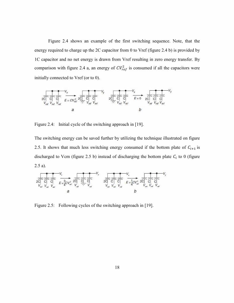
Figure 2.4 shows an example of the first switching sequence. Note, that the
energy required to charge up the 2C capacitor from 0 to Vref (figure 2.4 b) is provided by
1C capacitor and no net energy is drawn from Vref resulting in zero energy transfer. By
comparison with figure 2.4 a, an energy of is consumed if all the capacitors were
initially connected to Vref (or to 0).
Figure 2.4: Initial cycle of the switching approach in [19].
The switching energy can be saved further by utilizing the technique illustrated on figure
2.5. It shows that much less switching energy consumed if the bottom plate of is
discharged to Vcm (figure 2.5 b) instead of discharging the bottom plate to 0 (figure
2.5 a).
Figure 2.5: Following cycles of the switching approach in [19].
19
Chapter 3: Comparator
3.1 METRICS
ADC’s comparator compares two instantaneous analog voltages and generates
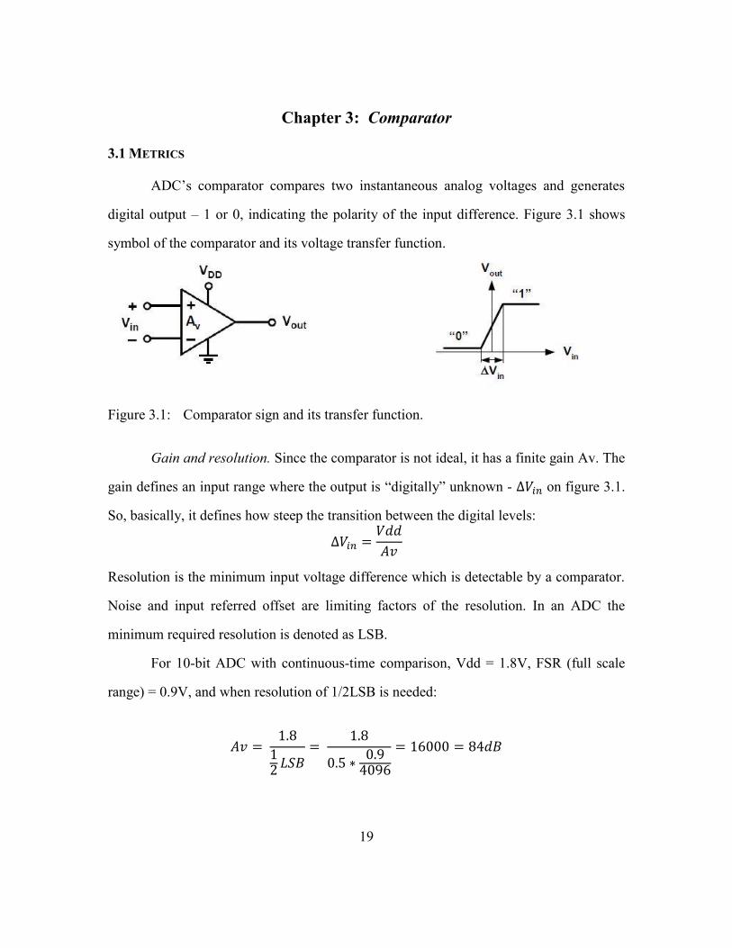
digital output – 1 or 0, indicating the polarity of the input difference. Figure 3.1 shows
symbol of the comparator and its voltage transfer function.
Figure 3.1: Comparator sign and its transfer function.
Gain and resolution. Since the comparator is not ideal, it has a finite gain Av. The
gain defines an input range where the output is “digitally” unknown - on figure 3.1.
So, basically, it defines how steep the transition between the digital levels:
Resolution is the minimum input voltage difference which is detectable by a comparator.
Noise and input referred offset are limiting factors of the resolution. In an ADC the
minimum required resolution is denoted as LSB.
For 10-bit ADC with continuous-time comparison, Vdd = 1.8V, FSR (full scale
range) = 0.9V, and when resolution of 1/2LSB is needed:

20
Input referred offset. Key performance metric of the comparator is input referred
offset voltage which limits accuracy of the comparator and consequently decreases
resolution of the ADC. Figure 3.2 shows how input referred offset can be modeled for a
two-stage comparator [5].
Figure 3.2: Two-stage comparator with offset modeling.
Relevant effects that contribute to the offset can be divided into static and
dynamic components [6-7]. The most commonly discussed sources of static offset
originate from threshold voltage mismatch and from mismatch in current factor (
). Sources of dynamic offset stem from mismatch in parasitic capacitances, and from
mismatch in load capacitances of back-to-back inverter latch. There is a range of methods
to reduce the input-referred offset: from simplest (increasing the width of input
transistors) to most complex (offset cancellation circuitry).
Kickback noise. Voltage disturbance at the input nodes of the comparator due to
large variation of the voltage at internal nodes is called kickback noise. Figure 3.3
illustrates kickback noise generation in a common dynamic latched comparator [8]. The
large voltage variations on the regeneration nodes are coupled through the parasitic
capacitance of the input NMOS to the input nodes of the comparator. Since the circuit

21
preceding the comparator does not have zero output impedance, the input signal is
disturbed.
Figure 3.3: Kickback noise modeling.
3.2 DYNAMIC LATCHED COMPARATOR
Dynamic latched comparators are widely used in SAR ADCs. Among its
attractive characteristics are fast speed, low power consumption, high input impedance,
full-swing output. Figure 3.4 illustrates a simple example of dynamic latched comparator.
It is also known as strong-arm sense amplifier [5] and as current-controlled latch sense
amplifier [7]. M1 and M2 are input transistors. M7, M8 are reset transistors. In reset
phase, when clock is low, reset transistors are on, so they charge the output nodes to
supply voltage. Tail transistor is off, thus no supply current flows through the differential
amplifier during the reset phase.

22
Figure 3.4: Strong-arm sense amplifier.
In regeneration phase, when clock is high, reset transistors are off, and the tail
transistor is turned on. The back-to-back inverters receive different amount of current
dependent on the input voltage and start to re-generate output. In other words, the drain
voltages of input transistors are getting discharged (from Vdd to ground) with different
slew rates depending on their gate voltages. Once the drain voltage (either of M1 or M2)
drops below (Vdd-Vth), NMOS of the inverter is turned on and the appropriate output
node starts to discharge. Since the output node is shorted to the input of another inverter,
PMOS of this inverter is turned on. Consequently, the output is regenerated - one node is
digital 1 while the other is 0.
Figure 3.5 shows a design with a slight addition to the above strong-arm latch-
based comparator [7]. In reset phase two additional PMOS transistors, M9 and M10,
supply Vdd to the drains of the input transistors. It increases the time period when input
transistors are in saturation during regeneration phase, which resulting in higher gain.

23
Figure 3.5: Dynamic latched comparator.
In the beginning of regeneration phase the current starts flowing in the pair, is
large, and the transistors are in saturation. By the end of regeneration phase both drains
of the differential pair approach 0 V potential and transistors enter triode region. So
during the whole operational cycle the drain nodes of the input pair have rail-to-rail
excursion plus transistors experience large variation in their operating region. These two
factors originate a large kickback noise [8] – one of the disadvantages of this comparator
type. Another drawback of the architecture is related to the fact that it has one tail
transistor. Size of the tail transistor limits the total current through differential input
branches and it should be increased in order to enhance the comparator speed. However,

24
dependent on a common-mode voltage, it decreases the time when input transistors are in
saturation which makes comparator gain lower and, in turn, input-referred offset more
significant. In other words, the speed and offset of this design are very dependent on
common mode input voltage [9]. Also, stack of four transistors in this comparator is an
additional possible issue for low supply technologies.
3.3 TWO-STAGE DYNAMIC LATCHED COMPARATOR
Two-stage dynamic latched comparator is designed to mitigate above issues. As
the name implies, the comparator consists of two stages – input-gain stage and output-
latch stage. This separation made the comparator to have a lower and more stable offset
voltage over a wide range of input common-mode voltage Vcm. Also the comparator can
operate at lower supply voltages. Figure 3.6 shows such design introduced in [9].
Figure 3.6: Double-tail latch-type voltage sense amplifier in [9].

25
During the reset phase transistors M7 and M8 pre-charge Di nodes to Vdd, which
in turns causes M10 and M11to discharge the output nodes to ground. When Clk = Vdd
the tail transistors M9 and M12 turn on. Common-mode voltage at Di nodes drops
monotonically with a rate defined by drain current of the tail M9 and by total capacitance
of the node: ⁄ . As a result, input dependent differential voltage will build
up. The intermediate stage formed by M10 and M11 passes to the cross-coupled
inverters. The inverters start to regenerate the voltage difference as soon as the common-
mode voltage at Di nodes is no longer high enough for M10, M11 to clamp the outputs to
ground. M10 and M11 also provide a shielding between input and output which makes
kickback noise lower. The signal and noise are integrated on Di nodes, resulting in an
SNR that increases while the common-mode voltage decreases.
Figure 3.7 shows another example of two-stage dynamic latched comparator with
different design of the second stage [10].

26
Figure 3.7: Two-stage dynamic latched comparator.
In regeneration phase when the common-mode voltage on and reaches a
threshold below Vdd the PMOS input transistors of the second stage turn on and the
signal is amplified onto and nodes. When and reach a certain common
mode, the second stage starts to regenerate. The overall voltage gain prior to regeneration
is high because of the double-gain structure.
Comparators shown on figures 3.6 and 3.7 require clock and inversion of the
clock for its operation. Timing of high accuracy between Clk and Clkb is required
because the second stage has to detect the voltage difference between the differential
outputs of the gain stage “right away”.
27
Chapter 4: Successive Approximation Register
4.1 SYNCHRONOUS SAR LOGIC
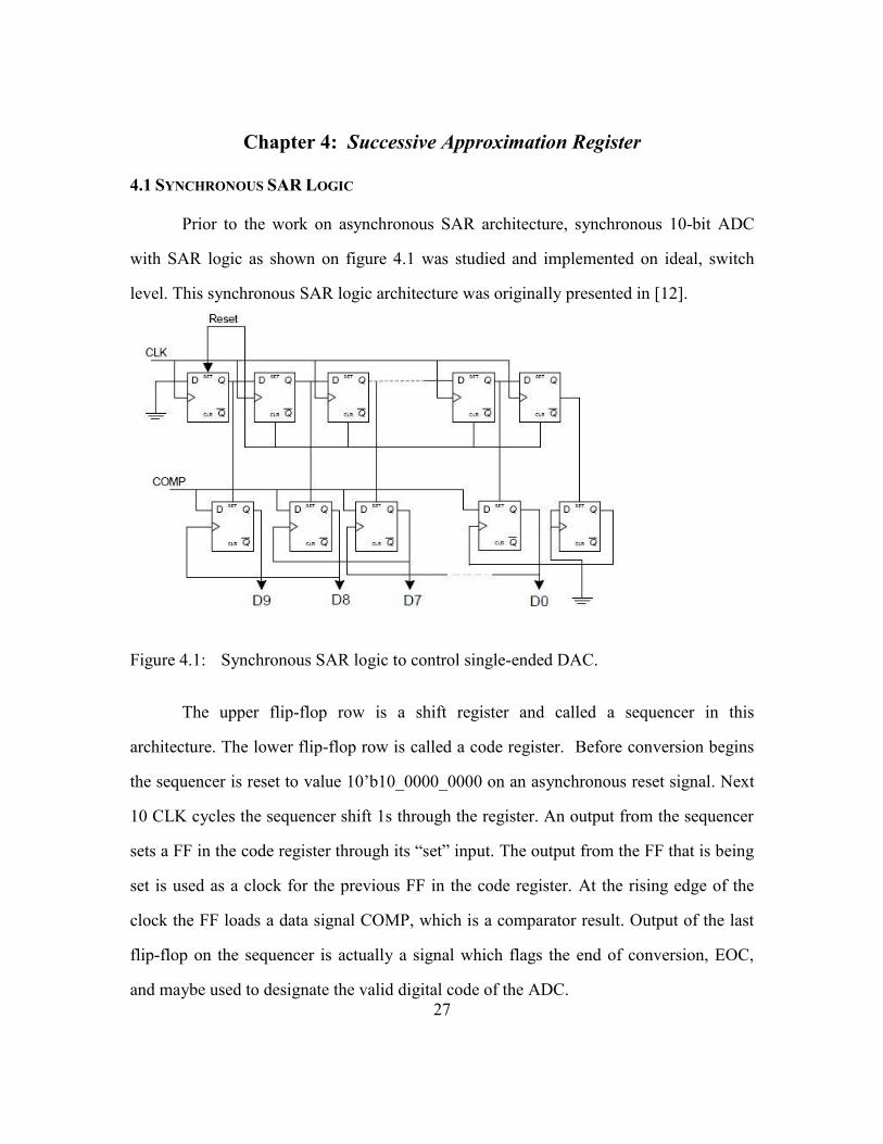
Prior to the work on asynchronous SAR architecture, synchronous 10-bit ADC
with SAR logic as shown on figure 4.1 was studied and implemented on ideal, switch
level. This synchronous SAR logic architecture was originally presented in [12].
Figure 4.1: Synchronous SAR logic to control single-ended DAC.
The upper flip-flop row is a shift register and called a sequencer in this
architecture. The lower flip-flop row is called a code register. Before conversion begins
the sequencer is reset to value 10’b10_0000_0000 on an asynchronous reset signal. Next
10 CLK cycles the sequencer shift 1s through the register. An output from the sequencer
sets a FF in the code register through its “set” input. The output from the FF that is being
set is used as a clock for the previous FF in the code register. At the rising edge of the
clock the FF loads a data signal COMP, which is a comparator result. Output of the last
flip-flop on the sequencer is actually a signal which flags the end of conversion, EOC,
and maybe used to designate the valid digital code of the ADC.

28
This type of SAR logic requires 2(N+1) flip-flops to control a capacitive DAC:
(N+1) - for the sequencer; (N+1) - for the code register.
Figure 4.2 shows a timing diagram for 3-bit synchronous SAR logic.
Figure 4.2: Timing diagram of 3-bit synchronous SAR logic.
Sampling clock (clks) is used for charging DAC capacitors and for SAR resetting.
The reset value is kept by SAR logic till the rising edge of CLK - SAR clock. SAR clock
(sar_clk) is a delayed version of comparator clock (clkc) to make sure that valid data
produced by the comparator is loaded by the code register. High level of clkc defines
regeneration phase of the comparator when it produces its outputs. Delay due to
comparator is not shown in the diagram. Synchronous SAR ADCs need a high rate clock
to make their SAR logic working. The frequency of the clock is at least N times higher
than the sampling clock. Its period has to be sufficient for the capacitive DAC to settle
and for the comparator to make correct decision. In the timing diagram for synchronous
design clkc is produced from such high frequency external clock.

29
4.2 ASYNCHRONOUS SAR LOGIC
Conceptually any SAR ADC works by following 3-step state machine while
testing a bit [21]. First, a new bit in the DAC is set. Second, a comparison is performed.
Third, the result determines which final value will be stored in the DAC register. In a
synchronous system these three steps are executed for each bit in succession in N
identical cycles by using oversampled clock. In an asynchronous system, self-
synchronization is used to achieve consecutive operation of these three steps.
The main idea behind asynchronous SAR ADC is illustrated on figure 4.3 [20].
Figure 4.3: Synchronous vs. Asynchronous SAR conversion.
In a synchronous design approximation time of MSB bit is equal to approximation time
of (MSB-1) bit and so on. This test time is set to accommodate the worst case time of bit

30
resolving. In an asynchronous design a data-ready signal is generated upon completion of
each comparison. Approximation time may vary from bit to bit, so the total conversion
phase is getting shorter, making possible an increase in sampling rate for the same
resolution. Since asynchronous approach eliminates the need for any internal clock,
significant power savings may be achieved. This architecture also easily trades off
conversion speed with resolution without significant power increase [20]. Asynchronous
approach takes more benefits from technology scaling, too – further improvements in
conversion time will be accomplished with the scaling.
One implementation of the asynchronous SAR logic is presented in [21], shown
on figure 4.4.
Figure 4.4: Asynchronous approach for SAR logic in [21].
In this system SAR logic functionally “split” in two parts: the main control and
the DAC control. Figure 4.5 details the functionality of main control and DAC control
slices. Conceptually, the main slice controls the timing of all N-bit comparisons in one
conversion cycle; and the DAC slice generates the bits based on the comparator output.

31
Figure 4.5: State machine of main control and DAC control.
There is one very important aspect with respect to DAC settling. Note, that the
main control requires bit_rdy to proceed with the operation. This signal is generated by
the DAC control on the positive output DACP. However the asserted bit_rdy does not
imply that the analog DAC output is settled. Proper DAC settling is not ensured by the
logic. In this particular design it is ensured by the fact that comparator reset phase, which
is happening in parallel to DAC settling, takes more time than the DAC settling.
Figure 4.6: Implementation of main control and DAC control.
Figure 4.6 shows implementation of the SAR slices by custom dynamic logic. It
requires the use of capacitors as memory elements to store the states. Here, these
capacitors (C1, C2, C3) are based entirely on the parasitic capacitance of an appropriate

32
transistor. So the sizing of these transistors is exclusively critical to have stored logic
levels reliable during the operation.
Figure 4.7: Asynchronous SAR architecture in [22].
Asynchronous systems in [22] and [23] use the same idea of a series of main slice
and DAC slice and implement those on dynamic logic. However, in [22], shown on
figure 4.7, the architecture is simplified by using complementary logic in addition to the
dynamic logic. Note that CK is a sampling clock, used to reset both arrays. BIT_SETs
start the comparison bit by bit; and EN enables the comparator operation.
Asynchronous SAR logic in [24], illustrated in figure 4.8, is implemented entirely
by complementary gates. This is a 9-bit ADC with differential input and top-plate
sampling DAC. CLK1 to CLK9 sample the digital comparator output and control DAC
capacitor arrays via N=9 DAC control logic parts. The first 8 control logic parts include a
D-FF, AND-gate, and a delay buffer to make sure that CLK triggers AND gate when the
D-FF output is valid. On a rising edge of CLK1-CLK9, D-FFs sample comparator output.
If it is low the relevant capacitor is kept connected to Vref, and if it is high the capacitor

33
is getting switched to Vss. At the falling edge of CLK1-CLK9, all capacitors are
reconnected to Vref.
Figure 4.8: Asynchronous SAR architecture in [24].

34
Chapter 5: Design of a 10-bit asynchronous SAR ADC
5.1 DAC
In this report binary-weighted capacitive fully-differential DAC was
implemented. The DAC is based on the bottom plate sampling. For 10-bit ADC the MSB
capacitors are of size 512*C. Unit capacitance C is of size 1 fF.
Top plate switch is needed to transmit voltage to the top plates of DAC
capacitors. This switch operates only during sampling phase. At the end of the conversion
the top plate potential is very close to Vcm. This means that the junction capacitance of
the top plate switch contributes very little nonlinearity to the system because its overall
voltage change is nearly zero [2, chapter 6]. During the sampling top plate switch is in
series with the entire array, it must have a low on-resistance, and hence large width, to
provide a fast acquisition. Top plate switch is implemented by a transmission gate, shown
on figure 5.1.
Figure 5.1: Top plate switch.
In this design SAR logic block generates digital signals dout[9:0] which control
DAC switches of positive and negative capacitor arrays. These switches transmit
or to the DAC capacitors. Since these reference voltages are set to and gnd,

35
digital inverters can be used as switches generating or for the bottom plate
network. In this design the input swing is nearly rail-to-rail. So transmission gates are
needed to sample input signal. Operation of the switches is described in table 5.1. Note
that clks, cycle and dout are purely digital signals.
clks cycle dout Vbottom_plate Description
1 x x Vin_n, Vin_p sampling phase
0 0 x Vcm keeping Vcm while waiting for i-th
conversion cycle to come to weigh Cs[i]
0 1 0 Vref_p, Vref_n conversion phase
0 1 1 Vref_n, Vref_p conversion phase
Table 5.1: Bottom plate switch operation for asynchronous SAR ADC
Figure 5.2: Bottom plate switch network for asynchronous SAR ADC.

36
Schematic of the bottom plate network for sampling capacitor Cs[i] for
asynchronous ADC is shown on figure 5.2. Note, that this switch network is for the
negative DAC array. It samples Vin_p. For the positive DAC array, which samples
Vin_n, the switch network has an additional invertor for dout. For synchronous SAR
architecture “cycle” does not exist. So the switch network shown above may be reused by
shorting cycle to Vdd. Switch network for dummy capacitor is simplified to one as on
figure 5.3.
Figure 5.3: Bottom plate network of Cdummy capacitor.
Transistor sizes for the switches are presented in table 5.2.
switch Wpmos, nm Lpmos, nm Wnmos, nm Lnmos, nm
S1 (dout) 1600 180 800 250
S2 750 180 350 180
S3, S6 (Vcm) 750 180 350 180
S4 750 180 350 180
S5, S7 (Vin) 850 180 400 180
dout, clksb, cycleb inverters 1400 180 650 180
Table 5.2: Sizing of the switches

37
5.2 COMPARATOR
Figure 5.4 shows schematic of the implemented comparator originally introduced
in [11]. This is a two stage dynamic latched comparator with two inverters inserted
between the stages to make voltage on nodes connecting the stages “stronger”, which
helps to increase regeneration speed.
Figure 5.4: Implemented comparator.
During the reset Di nodes are charged to Vdd and Di’ are discharged to ground.
PMOS transistors M10, M11, M14 and M15 are on and make Out and Sw nodes to be
charged to Vdd. NMOS transistors M12, M13 are off.
During regeneration or decision-making phase capacitance on Di nodes is
discharged from Vdd to ground with a different time rate which proportional to input
voltage. So, input dependent differential voltage is formed between Di nodes. When
either Di+ or Di- node voltage drops below Vdd-|Vthp|, the additional inverter (M18/M16

38
or M19/M17) inverts Di node signal into amplified Di’ node signal. Voltages on Di’
nodes are “different phased” and rising from 0 to Vdd with a different time interval.
Transistors M12, M13 turn on one after another and the final amplification is made
between Sw nodes before the regeneration process. When either Sw+ or Sw- voltage falls
below Vdd-Vthn, the latch starts to regenerate small voltage difference at Out nodes into
a full scale digital level:
= 1, = 0, if
= 0, = 1, if
The ideal operating point (Vcm), timing of the various phases and input offset
voltage can be tuned with the transistor sizes. Table 5.3 summarizes widths of the
comparator transistors.
Transistor Width, nm
M1/tail (nMOS) 220
M2, M3 (nMOS) – first differential pair 1200
M4, M5 (pMOS) – reset for first differential pair 300
M10, M11 (pMOS) – reset for latch 450
M14,M15 (pMOS) – reset for second differential pair 350
M6, M7 (nMOS) - latch 750
M8, M9 (pMOS) - latch 1500
M12, M13 (nMOS) – second differential pair 350
M16, M17 (nMOS) - inverter 350
M18, M19 (pMOS) - inverter 700
Table 5.3: Sizing of comparator transistors

39
For maximum voltage gain M1 (tail) may be dimensioned such that the first
differential pair operates in sub-threshold. Transistors that form regeneration latch (M6,
M7, M8, M9) and the inverter (M16, M17, M18, M19) impact speed of the comparator
most. “Reset” transistors, who supply Vdd to nodes during a reset phase, have different
width since found they impact differently on speed and noise performance. All transistors
of the comparator have minimum length of 180 nm.
5.3 TOP-LEVEL
Before going into the details of asynchronous SAR logic, it is better to look at the
design top-level, shown on figure 5.5. Differential analog input is sampled by the
capacitive DAC arrays. Sampling clock, clks, is an external master clock that can be at
Nyquist rate. When clks is at logic 1 the sampling is happening, as well as SAR digital
logic is under the internal reset condition. Falling edge of clks forms the first rising edge
of the comparator clock, clkc, after some delay.
Figure 5.5: Top-level of asynchronous 10-bit SAR.

40
Since the SAR logic in this ADC is asynchronous without using a high-frequency
clock generator, a “ready” indication from the comparator is used by combining two
complementary outputs of the comparator to control the timing of the logic. d and db are
pre-charged to Vdd. When comparator has worked in evaluation phase one of the two
outputs will go low. A NAND gate detects this high to low transition and generates an
active-high ready signal.
On the first rising edge of clkc the comparator falls into decision-making phase
for the first time. On the same edge SAR’s shift register asserts MSB cycle[9], which
controls MSB switch of the DAC arrays. The ready signal first triggers SAR’s code
register to produce an updated Dout[9:0]; second, it de-asserts current clkc; and third, it
asserts new clkc. The sequence continues till LSB cycle[0] gets 1’b1, which after a small
delay designates End-of-Conversion. EOC stops clkc until new sampling clock will
come. The ready signal and comparator data may be skewed to eliminate metastability
issues (please refer to SAR Code Register of 5.4).
ADC control and output blocks were not implemented, but it can be a good
addition to the design since then its operation may be controlled externally.
5.4 SAR LOGIC
clkc clock generator. Figure 5.6 shows schematic of a clock generator which
creates clock for SAR shift register and for the comparator.

41
Figure 5.6: CLKC clock generator.
D flip-flop with asynchronous reset and set is the main part of the generator.
During the ADC sampling phase, the generator does not produce a clock signal. Note,
that in this phase EOC is always 0, too, since it follows the reset condition of the SAR
logic during the sampling phase. AND gate between FF output and its clock is needed for
a case of an uncertain default value of the FF. When it is 1 AND gate places the first edge
of clkc at the right time (after ).
First rising edge of clkc happens almost after the falling edge of the clks. This
delay between the falling edge of clks and rising edge of clkc is equal to . Its value
is not very critical to the work of the logic. It only designates the beginning of a
conversion phase which follows a sampling phase.
and delays play important roles and their right values are critical.
is a delay after the comparator produced a valid data and it defines a falling edge
of clkc and, then, the pulse length of the valid comparator data itself. Value of has
to be long enough to give to the DAC enough time for settling. A new Dout bit is
produced on a rising edge of the ready signal. So the appropriate DAC settling happens
starting just after the ready signal assertion (code register delay and delay of the switches
have to be added). The settling must be finished before a new rising edge of clkc.

42
Note that the DAC settling and the reset phase of the comparator are happening
almost in parallel. To be precise, comparator reset is happening during
time. So we have to make sure that this is enough to reset the comparator.
Values of the three delays are estimated to = 3ns, = 5ns, = 15ns.
SAR shift register. Similar to the original synchronous SAR system shown on
figure 4.1, the asynchronous design has N-bit shift register, which clocked by clkc.
Schematic of this sequencer is on Figure 5.7.
Figure 5.7: SAR shift register.
SAR code register.
Figure 5.8: SAR code register.

43
Code register of the asynchronous SAR logic, shown on figure 5.8, works on a
rising edge of the ready signal. Since there are 10 edges per one conversion, each FF of
the register has to “know” when it is its turn to produce a valid bit of the code. Bus
bit[9:0] supplies this information. Asserted bit[9] “says”: “It is time to update Dout[9].
Do it on the following rising edge of your clock”. When the clock edge arrives, FF
number 9 updates its output by data d, which was “freshly” produced by the comparator.
This, apparently, the place, where metastability issues may appear, so ready skewing for
code register may be necessary.
Timing diagram on figure 5.9 summarizes the operation of the SAR logic block.
For simplicity, the diagram is corresponded to a 3-bit ADC, so cycle[2], bit[2] and
Dout[2] are the MSB providers in this case.
Note, that delay controls the width of last ready pulse. The last ready may be
chosen shorter than the previous ones. It’s still needed to be stronger to fire the last set of
Dout. However, the last comparison is already done for the conversion and we do not
need to wait for a DAC settling for a new approximation.

44
Figure 5.9: Timing diagram of the asynchronous SAR logic.
The following figures shows logic gates implemented for the work: D-FF with
asynchronous set and reset, XOR and MUX.

45
Figure 5.10: D-FF.
Figure 5.11: XOR and MUX gates.

46
Chapter 6: Simulations and Results
6.1 DAC
In this work binary-weighted capacitive fully-differential DAC, described in
section 5.1, was implemented. First, transistor-based DAC was validated in the ideal
environment, where comparator and SAR logic are introduced by ideal components,
provided by Dr. Nan Sun. In this environment the overall functionality of the ADC was
verified including degradation of SQNR from 61.9 dB. Figure 6.1 illustrates the DAC’s
functional performance in such environment.
Figure 6.1: DAC simulation in ideal-level environment.
DAC settling time is approximately 15 ns for the full swing input. Figure 6.2
zooms into the MSB evaluation.

47
Figure 6.2: DAC settling.
The following transient noise is made under the switching condition when
differential input is kept constant (Vin_p = 1.2V, Vin_n = 0.9V); sampling frequency is 5
MHz; internal self-timed clkc clock is 62.5 MHz.
To simulate switching noise of the DAC its output node was sampled. The
samples must to be done on the correct time instances – when DAC gives a settled
output. On figure 6.3 red highlights designate the 11 time instances, when DAC is
outputting a signal after all its switches and capacitors are settled. Note, that the last one
is not used by the comparator, but it does exit.

48
Figure 6.3: Time instances for DAC transient noise.
Figure 6.4 gives an example of the transient noise on the DAC output node for
different time instances.
Figure 6.4: DAC transient noise for the first 5 time instances.
Transient noise simulations were able to run only with moderate accuracy.
Conservative accuracy, or a moderate one but with a noise scale, crashed the simulator in

49
the middle of the run due to excessive memory usage (more than 6G), which exceeded
memory quota. The white noise was simulated with noise Fmax = 1GHz, which is more
than 15 times larger than the highest frequency of the system - internal self-timed clkc
clock. The simulation was run for 109 samples.
After the all 11 tables with the voltage variations on the DAC output node were
get, each table data was analyzed in JMP Pro tool to know noise value as a standard
deviation. Figure 6.5 shows an example of such analysis for the second sample.
Figure 6.5: DAC transient noise analysis for a time sample.
Figure 6.6 summarizes the noise data for the DAC’s upper capacitive array. It
shows that average noise on the positive DAC node is around 191 µV. If to take the same
number for the negative output node of the DAC, the switching noise of the whole DAC
may be approximated to around 380 µV.

50
Figure 6.6: Average transient noise of the DAC.
DAC power, measured as an average transient current on the DAC supply node
and multiplied by 1.8 V, is 31 µW. To this number should be added a power drawn from
Vcm supply (0.9 V) which is measured as 2.3 µW. The measurements are made for one
period of the full swing differential input with frequency Fs/64, where Fs = 5MHz.
6.2 COMPARATOR
In this work two-stage dynamic latched comparator, shown on figure 5.4, was
implemented. The validation of the comparator went in two ways. First, the transistor-
based comparator was inserted into ideal, switch-based ADC design instead of its ideal
presenter. The changes in the behavior of this ideal components design but with the real
comparator were checked, including degradations from ideal SQNR=61.9 dB. Since the
DAC was still ideal for the simulation, the real comparator insertion did not affect much
the outputs of the DAC.
In the second validation way, the comparator was simulated stand-alone by using
a testbench shown on figure 6.7.

51
Figure 6.7: Test-bench for the comparator validation.
The NAND gate is used to validate the timing of the comparator’s valid data
output. NAND gate is built by using minimum length and width CMOS transistors. Load
on the NAND is chosen as big as 100 fF to simulate a case when “ready” signal is used as
a clock for the code register of the asynchronous SAR logic. The same load value is
applied for comparator’s differential outputs, since in real design they (or one of them)
are heavy loaded by SAR’s code register data inputs.
Figure 6.8 illustrates comparator’s speed measurement. These measurements were
done for different Vcm voltages. It is found that there is about 600 ps from the rising
edge of the clock to the data output of the comparator. It takes almost 1650 ps from the
rising edge of the clock to the rising edge of ready. These numbers are for Vcm=0.9V and
input deltas bigger than 500 µV.

52
Figure 6.8: Comparator performance.
Figure 6.9 shows comparator behavior with smaller “deltas” between its inputs.
Figure 6.9: Drop due to small input delta.

53
Note how comparator’s db output drops from Vdd to below Vcm level.
Eventually it restores back to Vdd, but it impacts a lot the timing and the quality of the
ready signal. On the example it takes around 2.8 ns from the rising edge of the clock to
the rising edge of ready. The drops are significant (close to 0.9V), starting from deltas
300 µV and below for Vcm = 0.9V.
Besides of the overall functionality and performance of the comparator, the
testbench was used to run comparator noise analysis. Since the comparator is a dynamic
circuit, AC noise simulation and periodic steady-state (PSS) noise simulation do not
apply as there is no operating point and there is no steady-state here.
Noise simulation approach for dynamic comparators is introduced in [5, Voltage
Comparators] and used in the report. Transient noise simulations may be run for different
input “deltas” with values close to the noise level. Since transient noise is enabled, the
output of the comparator will defer from the expected from time to time, or sample to
sample. The smaller the delta the higher the probability of the wrong output. Table 6.1
and corresponded diagrams on figures 6.10, 6.11, 6.12 show the relationship seen for 100
samples. db deviations (drops) from ideal 1’b1 on every clock cycle are mentioned
above.
delta from Vcm, µV Probability of db to be equal to 1’b1
600 0.94% (100 total cycles – 6 cycles when db = 1’b0)
300 0.8% (100 total cycles – 20 cycles when db = 1’b0)
200 0.74% (100 total cycles – 26 cycles when db = 1’b0)
Table 6.1: Transient noise results

54
Figure 6.10: Transient noise when delta = 600 µV.
Figure 6.11: Transient noise when delta = 300 µV.
Figure 6.12: Transient noise when delta = 200 µV.
Now assume that comparator input referred noise follows normal distribution:
√ ∫
Take as a mean; and cumulative probability is P = 0.8. Standard
deviation = 2.56 correspond to P = 0.8. So random variable Vn, or input referred noise,
is spread to 353 µV. The result is achieved when noise Fmax = 1G, and the simulations
run for 100 samples.

55
Comparator power (average transient current on its supply node multiplied by
1.8V) is measured to 43 µW for the load of 100fF and under the switching condition
when differential input is kept constant, so only one of the comparator outputs switches
on each clock cycle.
6.3 SAR LOGIC
SAR digital logic, including ready’s NAND, shift register (figure 5.7), code
register (figure 5.8), is implemented on transistors. Delay elements of CLKC generator
(figure 5.6) are ideal components from the analogLib. As in the cases of the DAC and the
comparator, transistor-based SAR logic was validated in the ideal environment, first,
where the comparator and DAC switches are introduced by the ideal components. After
making sure that ADC’s functionality is ok, transistor-level DAC and transistor-level
comparator substituted their ideal-level presenters, making the SAR block inputs and
outputs to have realistic driver and load. Performance of the logic was measured in this
transistor-level environment. It is shown below on figure 6.15 of the “Top-Level and
Conclusions” section.
The following transient noise is made under the switching condition when
differential input is kept constant (Vin_p = 1.2V, Vin_n = 0.9V); sampling frequency is 5
MHz; internal self-timed clkc clock is 62.5 MHz; noise Fmax = 1G.
To simulate noise performance of the SAR logic its digital outputs were sampled.
The samples had to be done on the correct time instances – when SAR logic is supposed
to give an approximate bit for a current conversion. For MSB it happens just after the
first rising edge of clkc; for LSB it is, apparently, a time after the last clkc rising edge.
After the all 10 tables with the voltage variations on the digital levels were get, each table

56
data was analyzed in JMP tool to know noise value as a standard deviation. Figure 6.13
shows an example of such analysis for Dout bits 2, 3, 4.
Figure 6.13: Transient noise analysis for Dout bits.
Figure 6.14 summarizes the noise data for the digital logic, excluding delay lines.
It shows that average transient noise is around 293 µV.
Figure 6.14: Average transient noise of the SAR logic.

57
SAR power is measured as an average transient current on the digital logic supply
node and multiplied by 1.8 V, is 53 µW. The measurement is made for one period of the
full swing differential input with frequency Fs/64, where Fs = 5MHz.
6.4 TOP-LEVEL AND CONCLUSIONS
Figure 6.15 shows details of the timing of a one bit approximation.
Figure 6.15: Timing of the MSB approximation.

58
First rising edge of clkc happens after = 3ns plus some digital logic delay.
This clkc edge produces cycle[9] after 0.3 ns. It opens a switch of the DAC, so the DAC
output reacts immediately. There is 2ns between the rising edge of clkc and the rising
edge of the ready signal. The ready is a clock signal for the code register. On its rising
edge the new Dout bit is produced. There is about 2.5 ns between the rising edge of clkc
and the rising edge of the new code bit. At last, DAC starts its settling accordingly to the
new code.
For transistor-level design achieved ENOB is (50.1-1.76)/6.02 = 8.03. It is for
5MS/s sampling frequency and input range of 1.5V. To define what mostly impacts the
linearity, the same design runs but with slightly reduced unit capacitance. In the case
when the unit capacitance is 0.9 fF, ENOB = (51.6-1.76)/6.02 = 8.3.
Figure 6.16 shows 64-point FFT when input signal frequency is 1/64 of the
sampling one. Corresponding SFDR is 56.4 dB.
Figure 6.16: 64-point FFT.

59
Simulations of transistor-level design with higher input frequencies get
unexpectedly big amount of time. For example, simulation time for 32 periods of the
input signal with frequency 1/2Fs was approximated up to 25 hours. Experiments to run
SNR and SFDR analysis with ideal-level SAR logic, but transistor-level comparator and
DAC, were not successful, too – after some long hours of running the simulations were
killed due to excessive memory usage even for input of 5/64Fs. Also it is found that
SFDR of the design when only DAC on transistors is almost identical to the number
found above for the whole design (56.04 dB vs. 56.41 dB). Figure 6.17 shows FFT in this
case. For 5/64Fs for DAC only, SFDR degrades to 48 dB, which also proves that the
DAC is the main source of non-linearity in the design.
Figure 6.17: 64-point FFT, DAC only.

60
Table 6.3 summarizes power and noise performance of the design.
Power, µW Noise, µV
DAC 33 380
Comparator 43 353
CLKC generator (excluding delay lines) 2 n/a
SAR logic total 55 293
Table 6.3: Power and noise results
Here are key-learnings made from the research and implementation:
Asynchronous systems are very beneficial for applications where support for
oversampled clock is complicated or not possible. The asynchronous ADCs has
simpler IO interface than synchronous data convertors.
Asynchronous SAR logic relies on a comparator decision to proceed with its
consecutive operations. It implies that one comparator’s “hang” may introduce a
failure for the rest of a conversion. While in synchronous system, one failure of
the comparator breaks only single bit in the conversion.
Asynchronous SAR logic does not ensure proper DAC settling in an “automatic”
way. Appropriates delays in CLKC clock generator must be found from precise
transistor-level simulations.
In the asynchronous SAR design comparator reset-phase and DAC settling are
happening almost in parallel. If DAC settling time dominates, it is possible to
relax comparator performance requirements to save power.

61
Critical path through the digital logic has to be analyzed and the logic has to be
optimized with accordance to it. Non-critical gates are needed to be loosening to
save power.
Comparator’s transistors have to be tuned when it is placed together with
transistor-based DAC. Its behavior is different when it is driven by ideal-
components DAC.
Bootstrap circuits are necessary for front-end switches to improve DAC
performance.
Binary-weighted capacitive DAC is not the best choice for an asynchronous SAR
system of resolution 10-bit and higher. Speed and energy benefits of the
asynchronous system are fading by DAC settling. Other approaches need to be
considered as split-array, top-plate sampling, or different switching schemes
(refer to “Trends in Capacitive DAC Design” section).

62
Bibliography
[1] B. Murmann, P. Nikaeen, D.J. Connelly, R.W. Dutton. Impact of scaling on
analog performance and associated modeling needs. IEEE Transactions on
Electron Devices. Vol. 53, No. 9, September 2006.
[2] B. Razavi. Principles of data conversion system design. IEEE Press. 1995.
[3] Tuan-Vu Cao, Snorre Aunet, Trond Ytterdal. A 9-bit 50MS/s asynchronous SAR
ADC in 28 nm CMOS. IEEE 978-1-4673-2223-2/12. 2012.
[4] Dai Zhang, Ameya K Bhide, Atila Alvandpour. Design of CMOS sampling
switch for ultra-low power ADCs in biomedical applications. IEEE 978-1-4244-
8973-2/10. 2010.
[5] Nan Sun. Data converters. EE 382V. UT Austin. 2013.
[6] Amin Nikoozadeh, Boris Murmann. An analysis of latch comparator offset due to
load capacitor mismatch. IEEE Transactions on Circuits and Systems. Vol. 53,
No 12, December 2006.
[7] Tsuguo Kobayashi, Kazutaka Nogami, Tsukasa Shirotori, Yukihiro Fujimoto. A
current-controlled latch sense amplifier and a static power-saving input buffer for
low-power architecture. IEEE Journal of solid-state circuits, Vol. 28, No 4. 1993.
[8] Pedro M. Figueiredo, Joao C. Vital. Kickback noise reduction techniques for
CMOS latched comparators. IEEE Transactions on Circuits and Systems – II,
Vol. 53, No. 7. 2006.
[9] Daniel Schinkel, Eisse Mensink, Eric Klumperink, Ed van Tuijl, Bram Nauta. A
double-tail latch-type voltage sense amplifier with 18ps setup+hold time. 1-4244-
0852-0/07. IEEE International Solid-State Circuits Conference. 2007.
[10] Michiel van Elzakker, Ed van Tuijl, Paul Geraedts, Daniel Schinkel, Eric
Klumperink, Bram Nauta. A 1.9µW 4.4fJ/conversion-step 10b 1MS/s charge-
redistribution ADC. 978-1-4244-2011-7/08. IEEE International Solid-State
Circuits Conference. 2008.
[11] HeungJun Jeon, Yong-Bin Kim. A CMOS low-power low-offset and high-speed
fully dynamic latched comparator. 978-1-4244-6683-2/10. IEEE International
SOC Conference. 2010.
[12] T.O. Anderson. Optimum control logic for successive approximation analog-to-
digital converters. Communications Systems Research Section, JPL Technical
Report 32-1526, Vol XIII.
[13] Walt Kester. ADC architectures II: Successive Approximation ADCs. MT-021
tutorial. Analog Devices. 2008

63
[14] Understanding SAR ADCs: their architecture and comparison with other ADCs.
Maxim Integrated Tutorials at http://www.maximintegrated.com/app-
notes/index.mvp/id/1080
[15] R. Jacob Baker. CMOS circuit design, layout, and simulation. Third edition. IEEE
Series on Microelectronic Systems.
[16] Brian P. Ginsburg, Anantha P. Chandrakasan. Dual time-interleaved successive
approximation register ADCs for an ultra-wideband receiver. IEEE Journal of
solid-state circuits, Vol. 42, No 2, 2007.
[17] Brian P. Ginsburg, Anantha P. Chandrakasan. 500-MS/s 5-bit ADC in 65-nm
CMOS with split capacitor array DAC. IEEE Journal of solid-state circuits, Vol.
42, No 4, 2007.
[18] Yan Zhu, Chi-Hang Chan, U-Fat Chio, Sai-Weng Sin, Seng-Pan U, Rui Paulo
Martins, Franco Maloberti. Split-SAR ADCs: improved linearity with power and
speed optimization. IEEE transactions on VLSI systems, 1063-8210, 2013.
[19] Arindam Sanyal, Nan Sun. SAR ADC architecture with 98% reduction in
switching energy over conventional scheme. Electronics Letters, Vol. 49, 2013.
[20] Shuo-Wei Mike Chen, Robert W. Brodersen. A 6b 600MS/s 5.3mW
asynchronous ADC in 0.13µm CMOS. IEEE international solid-state circuits
conference, 1-4244-0079-1, 2006.
[21] Pieter J. A. Harpe, Cui Zhou, Yu Bi, Nick P. van der Meijs, Xiaoyan Wang,
Kathleen Philips, Guido Dolmans, Harmke de Groot. A 26 µW 8 bit 10 MS/s
asynchronous SAR ADC for low energy radios. IEEE journal solid-state circuits,
Vol. 46, No 7, 2011.
[22] Guanzhong Huang, Pingfen Lin. A 15fJ/conversion-step 8-bit 50 MS/s
asynchronous SAR ADC with efficient charge recycling technique.
Microelectronics Journal 43 (2012) 941-948, Elsevier 2012.
[23] Jinwoo Kim, Shin-II Lim, Kwang-Sub Yoon, Sangmin Lee. Design of a 12-b
asynchronous SAR CMOS ADC. IEEE 978-1-4577-0711-7/11, 2011.
[24] Tuan-Vu Cao, Snorre Aunet, Trond Ytterdal. A 9-bit 50MS/s asynchronous SAR
ADC in 28nm CMOS. IEEE 978-1-4673-2223-2/12, 2012.


![Nudge Policies and Negative Liberty by Olga Fjodorowa [2013]](https://img.pdfslide.us/doc/110x75/577cc0e11a28aba71191724f/nudge-policies-and-negative-liberty-by-olga-fjodorowa-2013.jpg)