Embed Size (px)
Citation preview
Novel metallic field-effect transistors
by
Ivan P. Krotnev
A thesis submitted in conformity with the requirementsfor the degree of Master of Applied Science
Graduate Department of Electrical and Computer EngineeringUniversity of Toronto
© Copyright 2013 by Ivan P. Krotnev

Abstract
Novel metallic field-effect transistors
Ivan P. Krotnev
Master of Applied Science
Graduate Department of Electrical and Computer Engineering
University of Toronto
2013
This thesis describes a novel concept for a field-effect transistor based on metallic channels.
Latest research demonstrates that the bulk (3D) properties of many materials begin
to change when confined to 2D sheets, or 1D nanowires. Particularly, the bandgap
increases and the density of states decreases. In this work, this effect is explored further
to demonstrate its application to field-effect transistors. Certain metals such as Gold
and Silver in these dimensions have extremely low density of states in particular energy
regions and through gate modulation can be partially depleted from electrons thus
creating conditions for field-effect. A simulation study of Gold channel FET demonstrates
ION/IOFF of 30 and superior current driving capability compared to the state-of-the art
22 nm SiGe ETSOI as well as 30 nm nanotube transistors.
i

ii
Dedication
To the memory of my grandfather who battled cancer during the course of my degree.
iii

iv
Acknowledgements
First of all, I would like to express my gratitude to my supervisor, Professor Sorin P.
Voinigescu, for providing me with this opportunity and for his patient guidance and
continuous support along the way. I am greatly indebted to him for the many discussions
we had on my research work and other interesting topics. His methodical and practical
approach to engineering and life has been of great value to me.
I owe many thanks to my colleagues in the electronics research group at the University
of Toronto with whom I had the fortune to work with. The long hours in BA4182
were made possible through the friendship and assistance of Andreea Balteanu, Guy
Alter, Stefan Shopov, Yingying Fu, Ioannis Sarkas, Hasan Al-Rubaye, and Valerio Adinolfi.
I would like to thank our collaborators in Europe, namely George Konstantinidis and
colleagues of FORTH Crete, Adrian Dinescu and Alexandru Muller of IMT Bucharest,
for help in defining the process flow and fabricating the gold resistor test structures.
I also would like to thank the team at Quantumwise for providing the simulation
software as well as answering various questions related to its use.
Last but not least, I would like to thank my parents, Petar and Milka, and my sister
Stanimira, for their love and encouragement.
v

vi
Contents
Abstract i
Dedication iii
Acknowledgements v
List Of Tables xi
List Of Figures xiii
Physical Constants xvii
Acronyms xix
1 Introduction 1
1.1 Motivation . . . . . . . . . . . . . . . . . . . . . . . . . . . . . . . . . . . 1
1.2 Device candidates beyond CMOS . . . . . . . . . . . . . . . . . . . . . . 7
1.2.1 Tunnel FET . . . . . . . . . . . . . . . . . . . . . . . . . . . . . . 7
1.2.2 2D crystal FET . . . . . . . . . . . . . . . . . . . . . . . . . . . . 7
1.2.3 Carbon nanotube FET . . . . . . . . . . . . . . . . . . . . . . . . 10
1.2.4 Junctionless FET . . . . . . . . . . . . . . . . . . . . . . . . . . . 11
1.2.5 Metallic channel FET . . . . . . . . . . . . . . . . . . . . . . . . . 12
1.3 Device dimensions at the scaling limit of Si CMOS . . . . . . . . . . . . 15
vii
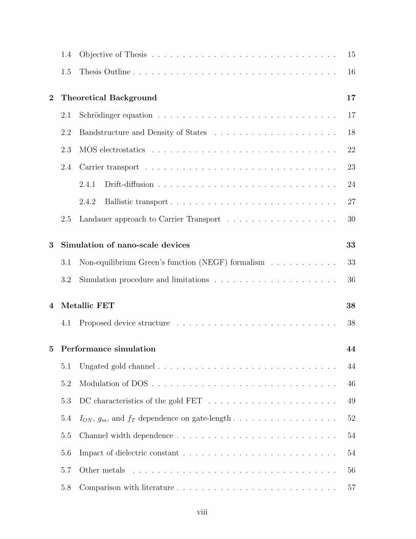
1.4 Objective of Thesis . . . . . . . . . . . . . . . . . . . . . . . . . . . . . . 15
1.5 Thesis Outline . . . . . . . . . . . . . . . . . . . . . . . . . . . . . . . . . 16
2 Theoretical Background 17
2.1 Schrodinger equation . . . . . . . . . . . . . . . . . . . . . . . . . . . . . 17
2.2 Bandstructure and Density of States . . . . . . . . . . . . . . . . . . . . 18
2.3 MOS electrostatics . . . . . . . . . . . . . . . . . . . . . . . . . . . . . . 22
2.4 Carrier transport . . . . . . . . . . . . . . . . . . . . . . . . . . . . . . . 23
2.4.1 Drift-diffusion . . . . . . . . . . . . . . . . . . . . . . . . . . . . . 24
2.4.2 Ballistic transport . . . . . . . . . . . . . . . . . . . . . . . . . . . 27
2.5 Landauer approach to Carrier Transport . . . . . . . . . . . . . . . . . . 30
3 Simulation of nano-scale devices 33
3.1 Non-equilibrium Green’s function (NEGF) formalism . . . . . . . . . . . 33
3.2 Simulation procedure and limitations . . . . . . . . . . . . . . . . . . . . 36
4 Metallic FET 38
4.1 Proposed device structure . . . . . . . . . . . . . . . . . . . . . . . . . . 38
5 Performance simulation 44
5.1 Ungated gold channel . . . . . . . . . . . . . . . . . . . . . . . . . . . . . 44
5.2 Modulation of DOS . . . . . . . . . . . . . . . . . . . . . . . . . . . . . . 46
5.3 DC characteristics of the gold FET . . . . . . . . . . . . . . . . . . . . . 49
5.4 ION , gm, and fT dependence on gate-length . . . . . . . . . . . . . . . . . 52
5.5 Channel width dependence . . . . . . . . . . . . . . . . . . . . . . . . . . 54
5.6 Impact of dielectric constant . . . . . . . . . . . . . . . . . . . . . . . . . 54
5.7 Other metals . . . . . . . . . . . . . . . . . . . . . . . . . . . . . . . . . 56
5.8 Comparison with literature . . . . . . . . . . . . . . . . . . . . . . . . . . 57
viii
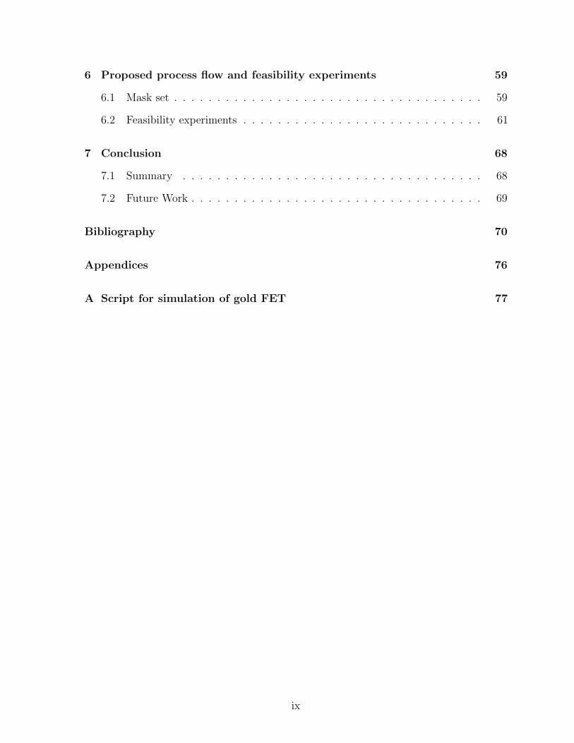
6 Proposed process flow and feasibility experiments 59
6.1 Mask set . . . . . . . . . . . . . . . . . . . . . . . . . . . . . . . . . . . . 59
6.2 Feasibility experiments . . . . . . . . . . . . . . . . . . . . . . . . . . . . 61
7 Conclusion 68
7.1 Summary . . . . . . . . . . . . . . . . . . . . . . . . . . . . . . . . . . . 68
7.2 Future Work . . . . . . . . . . . . . . . . . . . . . . . . . . . . . . . . . . 69
Bibliography 70
Appendices 76
A Script for simulation of gold FET 77
ix

x
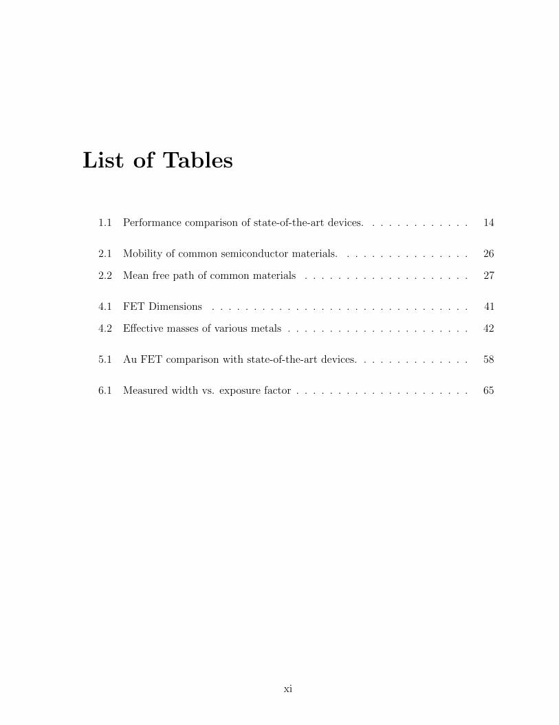
List of Tables
1.1 Performance comparison of state-of-the-art devices. . . . . . . . . . . . . 14
2.1 Mobility of common semiconductor materials. . . . . . . . . . . . . . . . 26
2.2 Mean free path of common materials . . . . . . . . . . . . . . . . . . . . 27
4.1 FET Dimensions . . . . . . . . . . . . . . . . . . . . . . . . . . . . . . . 41
4.2 Effective masses of various metals . . . . . . . . . . . . . . . . . . . . . . 42
5.1 Au FET comparison with state-of-the-art devices. . . . . . . . . . . . . . 58
6.1 Measured width vs. exposure factor . . . . . . . . . . . . . . . . . . . . . 65
xi

xii
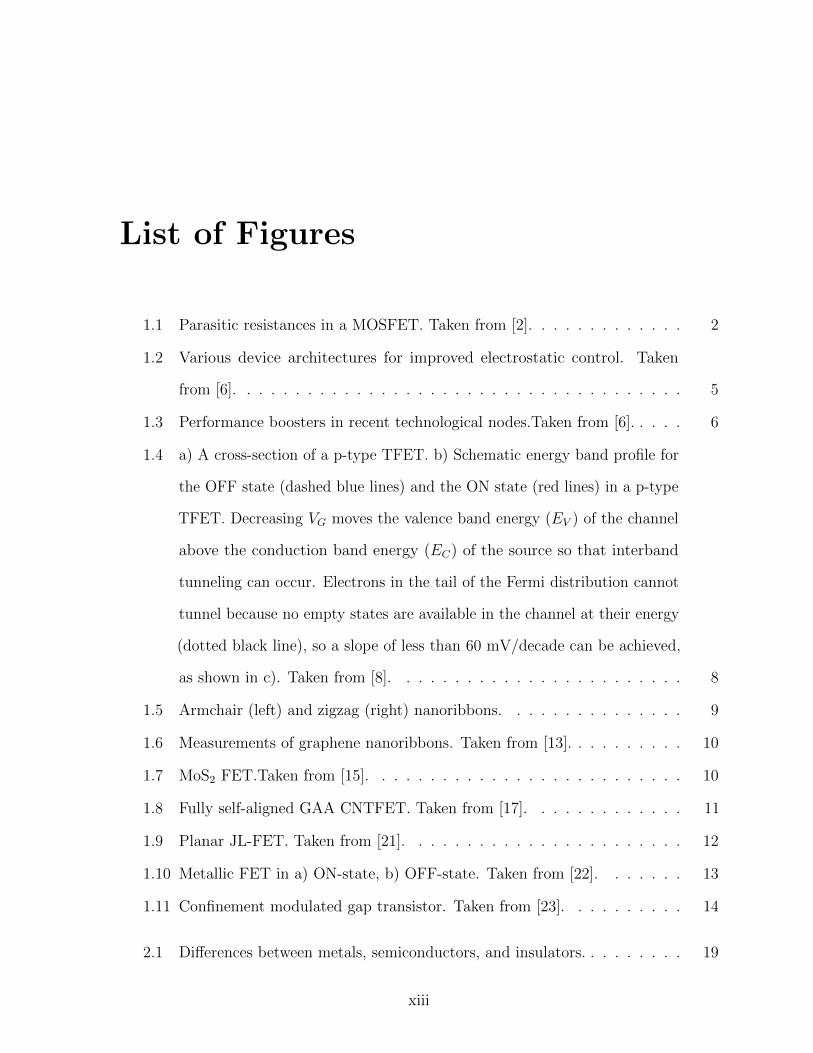
List of Figures
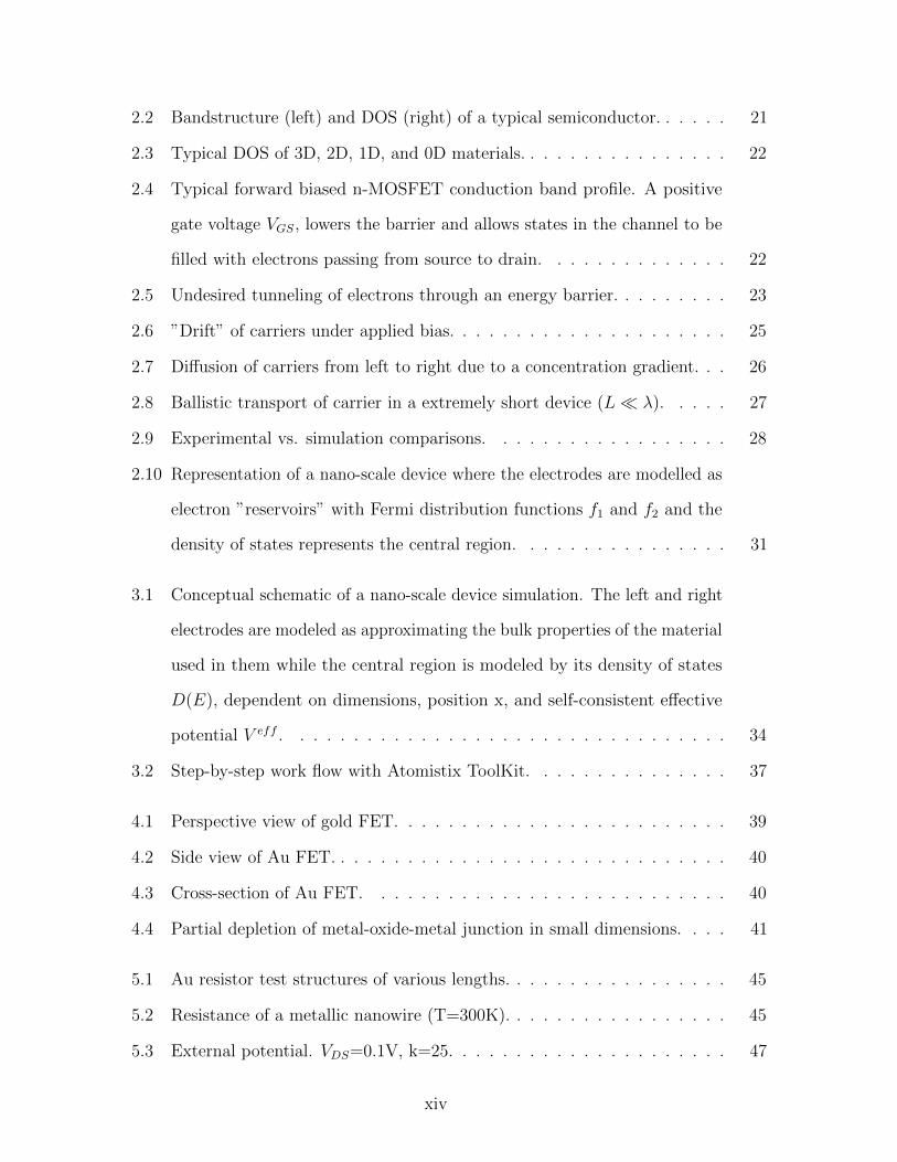
1.1 Parasitic resistances in a MOSFET. Taken from [2]. . . . . . . . . . . . . 2
1.2 Various device architectures for improved electrostatic control. Taken
from [6]. . . . . . . . . . . . . . . . . . . . . . . . . . . . . . . . . . . . . 5
1.3 Performance boosters in recent technological nodes.Taken from [6]. . . . . 6
1.4 a) A cross-section of a p-type TFET. b) Schematic energy band profile for
the OFF state (dashed blue lines) and the ON state (red lines) in a p-type
TFET. Decreasing VG moves the valence band energy (EV ) of the channel
above the conduction band energy (EC) of the source so that interband
tunneling can occur. Electrons in the tail of the Fermi distribution cannot
tunnel because no empty states are available in the channel at their energy
(dotted black line), so a slope of less than 60 mV/decade can be achieved,
as shown in c). Taken from [8]. . . . . . . . . . . . . . . . . . . . . . . . 8
1.5 Armchair (left) and zigzag (right) nanoribbons. . . . . . . . . . . . . . . 9
1.6 Measurements of graphene nanoribbons. Taken from [13]. . . . . . . . . . 10
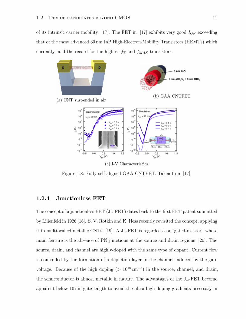
1.7 MoS2 FET.Taken from [15]. . . . . . . . . . . . . . . . . . . . . . . . . . 10
1.8 Fully self-aligned GAA CNTFET. Taken from [17]. . . . . . . . . . . . . 11
1.9 Planar JL-FET. Taken from [21]. . . . . . . . . . . . . . . . . . . . . . . 12
1.10 Metallic FET in a) ON-state, b) OFF-state. Taken from [22]. . . . . . . 13
1.11 Confinement modulated gap transistor. Taken from [23]. . . . . . . . . . 14
2.1 Differences between metals, semiconductors, and insulators. . . . . . . . . 19
xiii
2.2 Bandstructure (left) and DOS (right) of a typical semiconductor. . . . . . 21
2.3 Typical DOS of 3D, 2D, 1D, and 0D materials. . . . . . . . . . . . . . . . 22
2.4 Typical forward biased n-MOSFET conduction band profile. A positive
gate voltage VGS, lowers the barrier and allows states in the channel to be
filled with electrons passing from source to drain. . . . . . . . . . . . . . 22
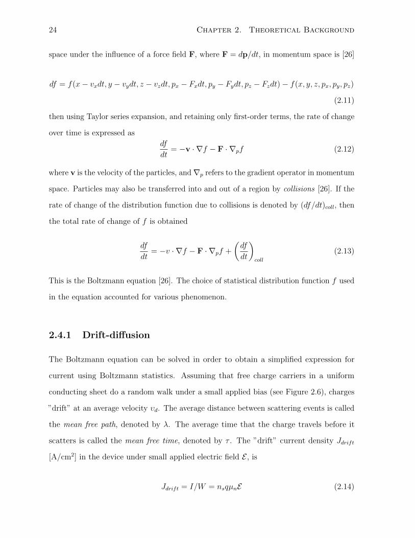
2.5 Undesired tunneling of electrons through an energy barrier. . . . . . . . . 23
2.6 ”Drift” of carriers under applied bias. . . . . . . . . . . . . . . . . . . . . 25
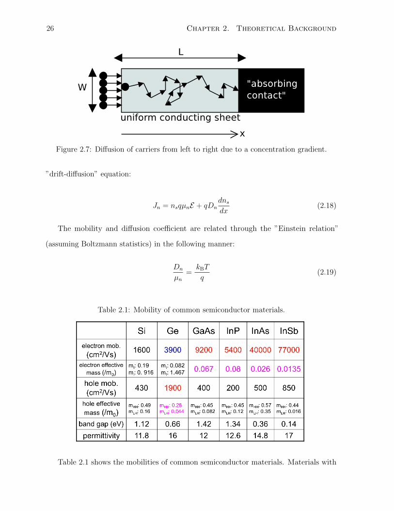
2.7 Diffusion of carriers from left to right due to a concentration gradient. . . 26
2.8 Ballistic transport of carrier in a extremely short device (L λ). . . . . 27
2.9 Experimental vs. simulation comparisons. . . . . . . . . . . . . . . . . . 28
2.10 Representation of a nano-scale device where the electrodes are modelled as
electron ”reservoirs” with Fermi distribution functions f1 and f2 and the
density of states represents the central region. . . . . . . . . . . . . . . . 31
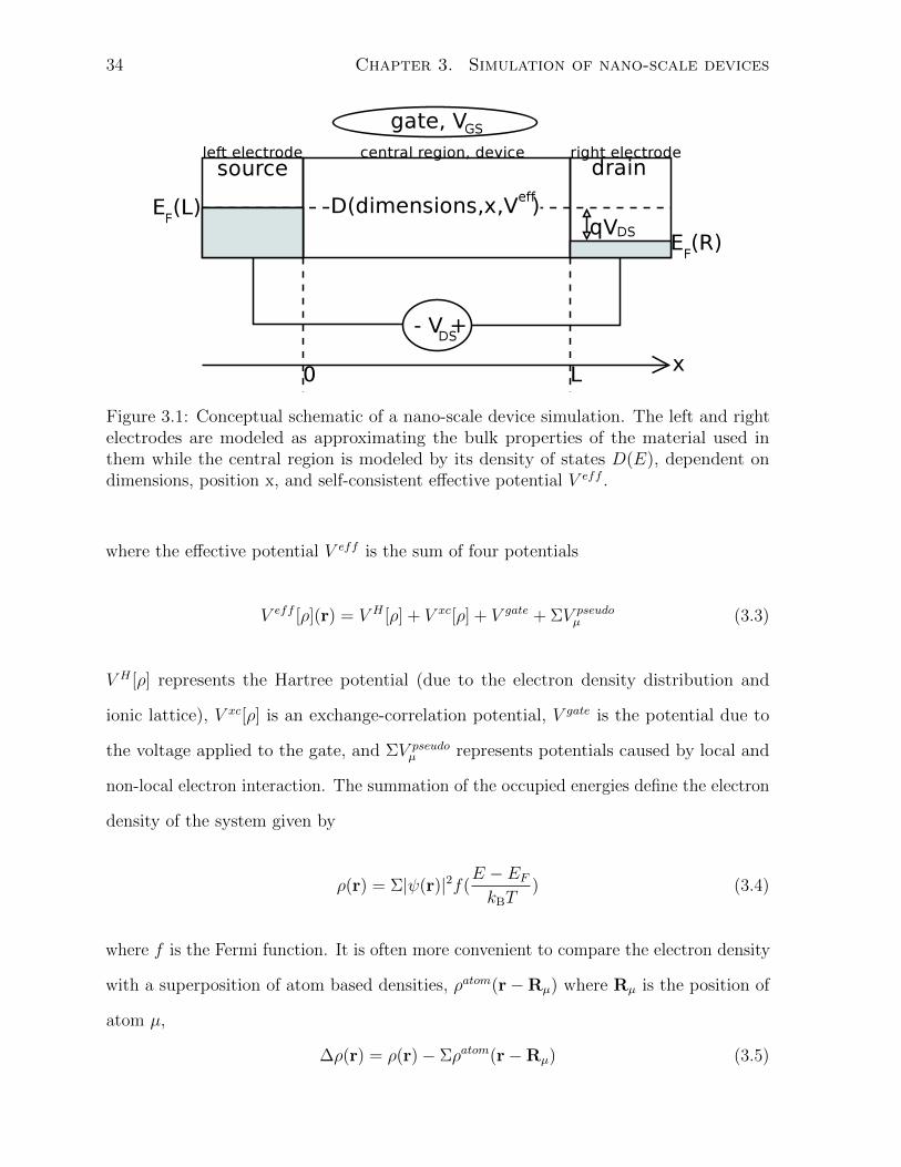
3.1 Conceptual schematic of a nano-scale device simulation. The left and right
electrodes are modeled as approximating the bulk properties of the material
used in them while the central region is modeled by its density of states
D(E), dependent on dimensions, position x, and self-consistent effective
potential V eff . . . . . . . . . . . . . . . . . . . . . . . . . . . . . . . . . 34
3.2 Step-by-step work flow with Atomistix ToolKit. . . . . . . . . . . . . . . 37
4.1 Perspective view of gold FET. . . . . . . . . . . . . . . . . . . . . . . . . 39
4.2 Side view of Au FET. . . . . . . . . . . . . . . . . . . . . . . . . . . . . . 40
4.3 Cross-section of Au FET. . . . . . . . . . . . . . . . . . . . . . . . . . . 40
4.4 Partial depletion of metal-oxide-metal junction in small dimensions. . . . 41
5.1 Au resistor test structures of various lengths. . . . . . . . . . . . . . . . . 45
5.2 Resistance of a metallic nanowire (T=300K). . . . . . . . . . . . . . . . . 45
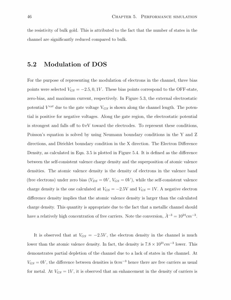
5.3 External potential. VDS=0.1V, k=25. . . . . . . . . . . . . . . . . . . . . 47
xiv
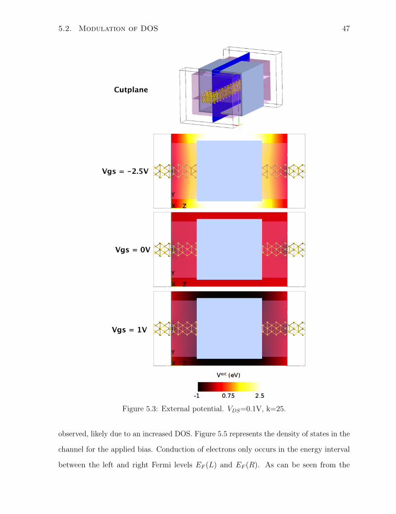
5.4 Electron Difference density. VDS = 0.1V, εr = 25. . . . . . . . . . . . . . . 48
5.5 Modulation of DOS in metals. . . . . . . . . . . . . . . . . . . . . . . . . 49
5.6 Transfer characteristics of Au FET. . . . . . . . . . . . . . . . . . . . . . 50
5.7 Output characteristics of Au FET. . . . . . . . . . . . . . . . . . . . . . 51
5.8 Length dependence of Au FET. . . . . . . . . . . . . . . . . . . . . . . . 52
5.9 gm of Au FET. . . . . . . . . . . . . . . . . . . . . . . . . . . . . . . . . 53
5.10 fT of Au FET. . . . . . . . . . . . . . . . . . . . . . . . . . . . . . . . . 53
5.11 Gate width variation. . . . . . . . . . . . . . . . . . . . . . . . . . . . . . 54
5.12 High-k dielectric variance. . . . . . . . . . . . . . . . . . . . . . . . . . . 55
5.13 Impact of a single layer of HfO2 on the conductance of the channel. . . . 55
5.14 Transfer characteristics of various metallic channels with identical dimensions. 56
5.15 Transfer characteristics of Sn FET. . . . . . . . . . . . . . . . . . . . . . 57
6.1 Definition of back gate, channel, and dielectric surrounding the channel. . 60
6.2 Definition of top gate and source/drain contact regions. . . . . . . . . . . 61
6.3 Top level layout of the fabricated resistor test structures. The alignment
mark is labelled X and is located in the bottom left corner. . . . . . . . . 62
6.4 Top level layout. The squares indicate locations with resistors. The squares
marked as ”short” or ”open” indicate shorted or open resistors, respectively.
The alignment mark is labelled X and is located in the bottom left corner.
The x-axis indicates the resistor length, the y-axis indicates the resistor
exposure factor during e-beam lithography. There are two Tiles with
identical structures. . . . . . . . . . . . . . . . . . . . . . . . . . . . . . . 63
6.5 (a) Zoomed out and (b) zoomed in view of sample resistor test structure
with (c) 45 nm width and (d) 60 nm length. . . . . . . . . . . . . . . . . . 64
6.6 Measured data of 40 nm gold resistors. . . . . . . . . . . . . . . . . . . . 66
6.7 Measured data of 0.8 exposure factor gold resistors. . . . . . . . . . . . . 66
6.8 Quantum of conductance leap while measuring the smallest fabricated device. 67
xv

xvi

Physical Constants
Boltzmann constant ( kB) 1.38× 10⁻²³ J/K.
Elementary charge (q) 1.602× 10⁻¹⁹ C.
Free electron mass (m0) 9.10953× 10⁻³¹ kg.
Permittivity of free space (ε0) 8.854× 10⁻¹² F/m.
Planck constant (h) 6.626× 10⁻³⁴ J s.
Quantum of conductance (q2/h) 39.6 µS.
Reduced Planck constant (~) 1.055× 10⁻³⁴ J s.
Thermal voltage ( kBT/q) 25.85 mV (room temperature).
xvii

xviii
Acronyms
ATK Atomistix ToolKit.
CMGT Confinement modulated gap transistor.
CMOS Complementary metal-oxide-semiconductor.
CNTFET Carbon nanotube field-effect transistor.
DFT Density functional theory.
DOS Density of states.
EOT Effective oxide thickness.
GAA Gate-all-around.
HEMT High-electron-mobility transistor.
ITRS International Technology Roadmap for Semiconductors.
JL-FET Junctionless field-effect transistor.
METFET Metallic channel field-effect transistor.
MOSFET Metal-oxide-semiconductor field-effect transistor.
NEGF Non-equilibrium Green’s function formalism.
SOI Silicon-on-insulator.
SS Subthreshold slope.
TFET Tunneling field-effect transistor.
xix

xx
Chapter 1
Introduction
1.1 Motivation
The demand for ever more powerful computers has led to the development of ex-
tremely small, nano-meter in size, metal-oxide-semiconductor field-effect transistors
(MOSFETs) [1]. However, this cannot continue indefinitely. Several fundamental and
physical limits make the performance improvement of these devices an extraordinarily
difficult engineering feat in the coming years. Some of these challenges include:
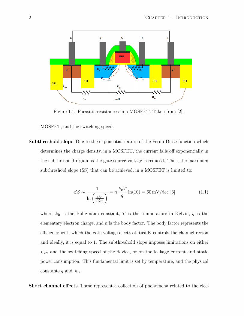
Drain/Source resistance The interface between the source/drain contact metal in the
highly-doped semiconductor adds parasitic resistance. In deeply scaled MOSFETs
these resistances (RS, and RD) significantly degrade ION , gm, fT, and fMAX (key
figures of merit for switching and high-frequency performance). This problem has
become prominent over the last decade when source and drain resistances have
become the bottleneck for performance improvement. The typical source/drain
resistance today is 200 Ω× µm of gate width.
Current driving capability Due to increasing doping concentration in the channel,
the mobility of electrons is degraded and, therefore, the maximum transistor current,
ION . This degradation affects the capacitive load that can be driven by a single
1
2 Chapter 1. Introduction
Figure 1.1: Parasitic resistances in a MOSFET. Taken from [2].
MOSFET, and the switching speed.
Subthreshold slope Due to the exponential nature of the Fermi-Dirac function which
determines the charge density, in a MOSFET, the current falls off exponentially in
the subthreshold region as the gate-source voltage is reduced. Thus, the maximum
subthreshold slope (SS) that can be achieved, in a MOSFET is limited to:
SS ∼ 1
ln
(dIDdVGS
) = nkBT
qln(10) = 60 mV/dec [3] (1.1)
where kB is the Boltzmann constant, T is the temperature in Kelvin, q is the
elementary electron charge, and n is the body factor. The body factor represents the
efficiency with which the gate voltage electrostatically controls the channel region
and ideally, it is equal to 1. The subthreshold slope imposes limitations on either
ION and the switching speed of the device, or on the leakage current and static
power consumption. This fundamental limit is set by temperature, and the physical
constants q and kB.
Short channel effects These represent a collection of phenomena related to the elec-
1.1. Motivation 3
trostatic control of the channel charge by the gate voltage. They include the short
channel effect, the reverse short channel effect, and the drain-induced barrier lower-
ing [3], all of which arise when the gate length becomes increasingly shorter leading
to a greater proportion of the channel charge being controlled by the source-bulk
and source-drain depletion regions. A detailed explanation of short channel effects
can be found in [2].
Over the last 10 years, a number of technological improvements have been implemented
in complementary metaloxidesemiconductor (CMOS) technology to overcome problems
mentioned above. These include:
Strain engineering for channel mobility boosting When strain is applied to a crys-
tal of certain orientation in a particular direction and orientation, the hole or electron
mobility can be increased. Although, strain can be used to overcome degradation
due to source and drain resistances and due to the increasing doping concentrations
in the channel, strain has a diminishing impact as the gate length is decreased
and its continued effectiveness is questionable below 14 nm. In a recent paper on
silicon-on-insulator (SOI) FinFETs with 14 nm gate length, it was reported that the
channel strain is only effective along the 〈110〉 direction [4]. In the 〈100〉 direction,
the benefits of strain vanish due to ballistic transport because the preexisting quan-
tum confinement already segregates most carriers into low effective mass valleys
[4].
High-K gate dielectrics and metal gate In a first order approximation, the gate-
channel capacitance is modelled as a parallel plate capacitor
C =kε0A
t(1.2)
where k (also labelled as εr) is the relative dielectric constant of the gate oxide
material, ε0 is the permitivity of free space, A is the area, and t is the dielectric
4 Chapter 1. Introduction
thickness of the capacitor. At thicknesses of 1.2− 1.5 nm, a traditional SiO2/SiON
gate oxide dielectric begins to exhibit very large leakage current. Since gate-length
scaling requires a commensurate scaling of the gate oxide thickness, this is the
main motivation for the introduction of alternative dielectric materials [5]. By
introducing a high-k dielectric one can reduce the gate leakage current by increasing
the physical thickness of the oxide, while maintaining a high gate capacitance, as
needed to control the channel charge. Possible candidates for the gate dielectric
are Al2O3, ZrO2, HfO2, Ta2O5, and any combination of them. From these, the
most successful has been HfO2 because of its ease of deposition by ALD [5] and
integration into the metal-gate CMOS flow.
Some of the challenges associated with high-k dielectrics are [5]:
1. Threshold voltage control - the threshold voltage control becomes different for
pMOS and nMOS devices, and different gate metals must be used.
2. Threshold voltage instability - by applying a pulsed voltage on the gate the
threshold tends to shift marginally.
3. Mobility and transistor performance - it is found that the carrier mobility in
the channel for both nMOSFETs and pMOSFETs decreases when a high-k
dielectric is used compared to conventional SiO2 + SiON.
The key issues which complicate the use of high-k materials described above have
been solved by replacing the polysilicon gate with a metal gate. By using different
metals for pMOSFETs and nMOSFETs, the threshold voltage control is elegantly
solved. Unfortunately, the HfO2/Si interface creates trap sites, which lead to
increased scattering and mobility degradation in the channel. For this reason,
state-of-the art MOSFETs at 45 nm and below, still require 2-3 atomic layers of
SiO2 and SiON between the Si surface and HfO2 layer.
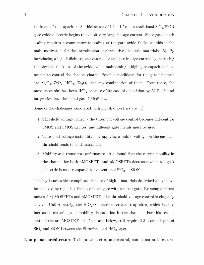
Non-planar architecture To improve electrostatic control, non-planar architectures
1.1. Motivation 5
such as the ones in Figure 1.2 have been introduced below 28 nm gate lengths.
Figure 1.2: Various device architectures for improved electrostatic control. Taken from [6].
These architectures improve the gate-to-channel capacitance by increasing the
surface area in Eq. 1.2. Currently, double-gate architecture has been adopted at
the 28 nm node along with SOI structures by a consortium lead by ST and IBM,
and the TriGate architecture has been chosen by Intel in the production 22 nm and
upcoming 14 nm nodes.
Alternative channel materials Silicon has been the workhorse of the integrated circuit
industry. Alternative channel materials have been proposed over the years with
better carrier mobility. However, due to economic factors, they remain largely
unused except for select applications, such as high-power or high-frequency low-
noise applications.
Figure 1.3 shows the incremental increases in performance and the performance
boosting techniques used at each node during the last decade. It is clear that, to improve
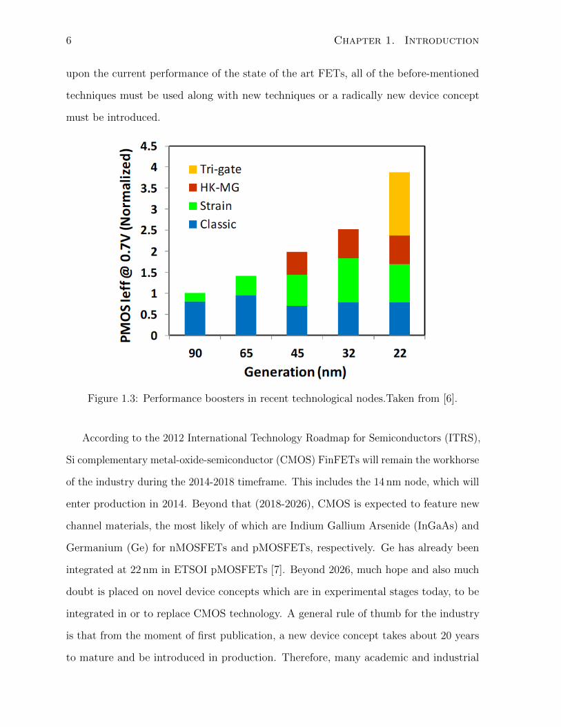
6 Chapter 1. Introduction
upon the current performance of the state of the art FETs, all of the before-mentioned
techniques must be used along with new techniques or a radically new device concept
must be introduced.
Figure 1.3: Performance boosters in recent technological nodes.Taken from [6].
According to the 2012 International Technology Roadmap for Semiconductors (ITRS),
Si complementary metal-oxide-semiconductor (CMOS) FinFETs will remain the workhorse
of the industry during the 2014-2018 timeframe. This includes the 14 nm node, which will
enter production in 2014. Beyond that (2018-2026), CMOS is expected to feature new
channel materials, the most likely of which are Indium Gallium Arsenide (InGaAs) and
Germanium (Ge) for nMOSFETs and pMOSFETs, respectively. Ge has already been
integrated at 22 nm in ETSOI pMOSFETs [7]. Beyond 2026, much hope and also much
doubt is placed on novel device concepts which are in experimental stages today, to be
integrated in or to replace CMOS technology. A general rule of thumb for the industry
is that from the moment of first publication, a new device concept takes about 20 years
to mature and be introduced in production. Therefore, many academic and industrial
1.2. Device candidates beyond CMOS 7
research groups today are investigating candidate concepts for the 2026 time period and
beyond. This is also the primary scope of this thesis.
1.2 Device candidates beyond CMOS
The following is a survey of the competing device concepts beyond CMOS.
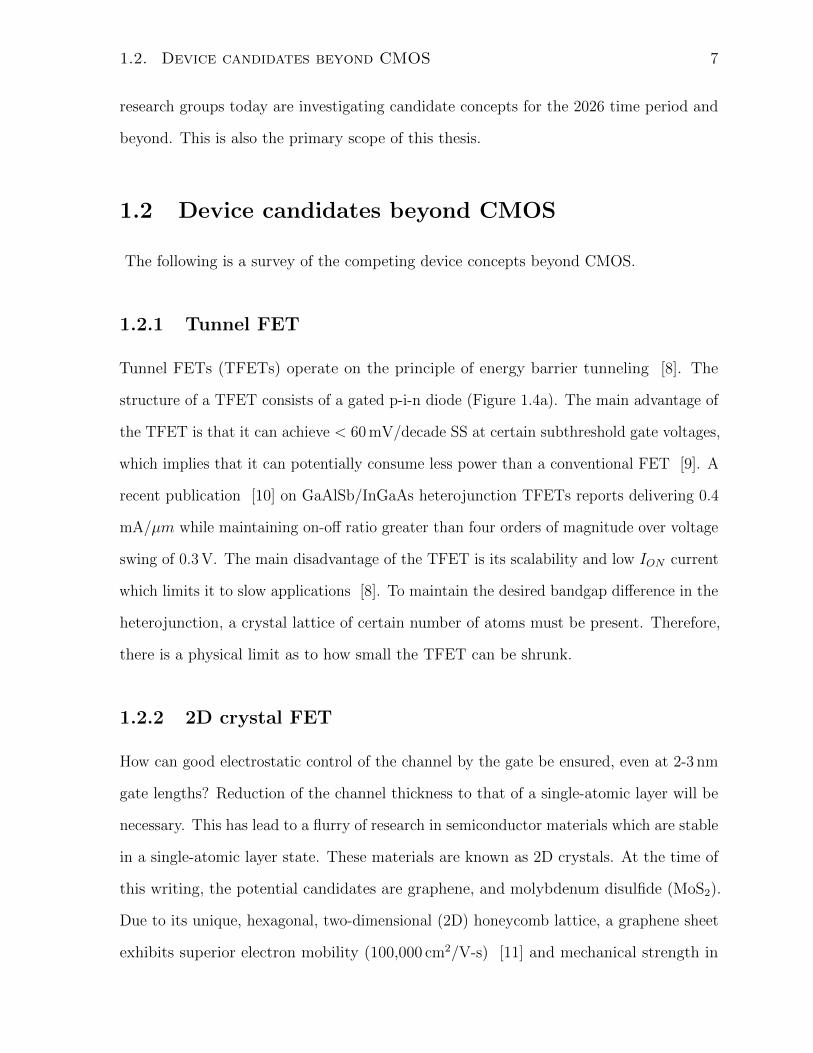
1.2.1 Tunnel FET
Tunnel FETs (TFETs) operate on the principle of energy barrier tunneling [8]. The
structure of a TFET consists of a gated p-i-n diode (Figure 1.4a). The main advantage of
the TFET is that it can achieve < 60 mV/decade SS at certain subthreshold gate voltages,
which implies that it can potentially consume less power than a conventional FET [9]. A
recent publication [10] on GaAlSb/InGaAs heterojunction TFETs reports delivering 0.4
mA/µm while maintaining on-off ratio greater than four orders of magnitude over voltage
swing of 0.3 V. The main disadvantage of the TFET is its scalability and low ION current
which limits it to slow applications [8]. To maintain the desired bandgap difference in the
heterojunction, a crystal lattice of certain number of atoms must be present. Therefore,
there is a physical limit as to how small the TFET can be shrunk.
1.2.2 2D crystal FET
How can good electrostatic control of the channel by the gate be ensured, even at 2-3 nm
gate lengths? Reduction of the channel thickness to that of a single-atomic layer will be
necessary. This has lead to a flurry of research in semiconductor materials which are stable
in a single-atomic layer state. These materials are known as 2D crystals. At the time of
this writing, the potential candidates are graphene, and molybdenum disulfide (MoS2).
Due to its unique, hexagonal, two-dimensional (2D) honeycomb lattice, a graphene sheet
exhibits superior electron mobility (100,000 cm2/V-s) [11] and mechanical strength in
8 Chapter 1. Introduction
Figure 1.4: a) A cross-section of a p-type TFET. b) Schematic energy band profile for theOFF state (dashed blue lines) and the ON state (red lines) in a p-type TFET. DecreasingVG moves the valence band energy (EV ) of the channel above the conduction band energy(EC) of the source so that interband tunneling can occur. Electrons in the tail of theFermi distribution cannot tunnel because no empty states are available in the channel attheir energy (dotted black line), so a slope of less than 60 mV/decade can be achieved, asshown in c). Taken from [8].
comparison to the highest-mobility III-V semiconductor InSb, which has mobility of
80,000 cm2/V-s. Unfortunately, to date, two main challenges have prevented researchers
from building a high performance transistor in these materials. First, graphene loses its
high mobility when deposited on an insulator such as SiO2. Second, the lack of inherent
bandgap in graphene makes it impossible to switch off a FET with graphene channel.
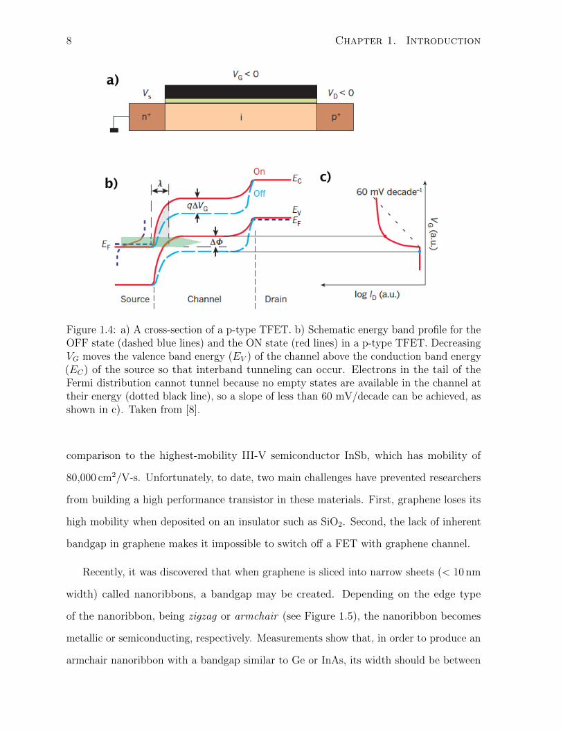
Recently, it was discovered that when graphene is sliced into narrow sheets (< 10 nm
width) called nanoribbons, a bandgap may be created. Depending on the edge type
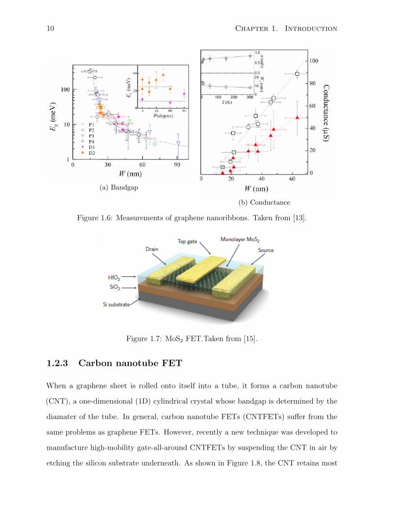
of the nanoribbon, being zigzag or armchair (see Figure 1.5), the nanoribbon becomes
metallic or semiconducting, respectively. Measurements show that, in order to produce an
armchair nanoribbon with a bandgap similar to Ge or InAs, its width should be between
1.2. Device candidates beyond CMOS 9
2 and 3 nm [12]. For bandgaps comparable to Si, InP, or GaAs, the width should be
reduced to 1 − 2 nm [12]. Unfortunately, as seen in Figure 1.6, with the creation of
bandgap, conductance experiences a significant drop due to severe mobility degradation.
Figure 1.5: Armchair (left) and zigzag (right) nanoribbons.
The best performance reported for graphene transistors is an intrinsic (discounting
RS, RD) fT of 200GHz and an ION/IOFF ratio of 3-4. However, the real, measured, fT
was less than 10GHz [14].
MoS2 features electron mobility of 200 cm2/V-s and a direct bandgap of 1.2 eV. A
typical transistor performance is expected with ION/IOFF of 106 [15]. Although electron
mobility is lower than in Si, the advantage of this material over Si is that its extremely
thin (monolayer). However, studies have shown that, as with graphene, when placed on an
insulating substrate such as SiO2, the mobility of MoS2 further drops to 0.1-10 cm2/V-s
[15] and is significantly inferior to that of Si thin films. While surface scattering is a
problem even in thin Si layers, in single-layered materials it will be a major issue. To
alleviate surface scattering, various techniques have been researched, the most promising
of which is to stack several single-layer materials. It was found that the mobility of
graphene is 60,000 cm2/V-s when the material is sandwiched between two sheets of boron
nitride (BN), a single-layer insulating material [16].
10 Chapter 1. Introduction
(a) Bandgap
(b) Conductance
Figure 1.6: Measurements of graphene nanoribbons. Taken from [13].
Figure 1.7: MoS2 FET.Taken from [15].
1.2.3 Carbon nanotube FET
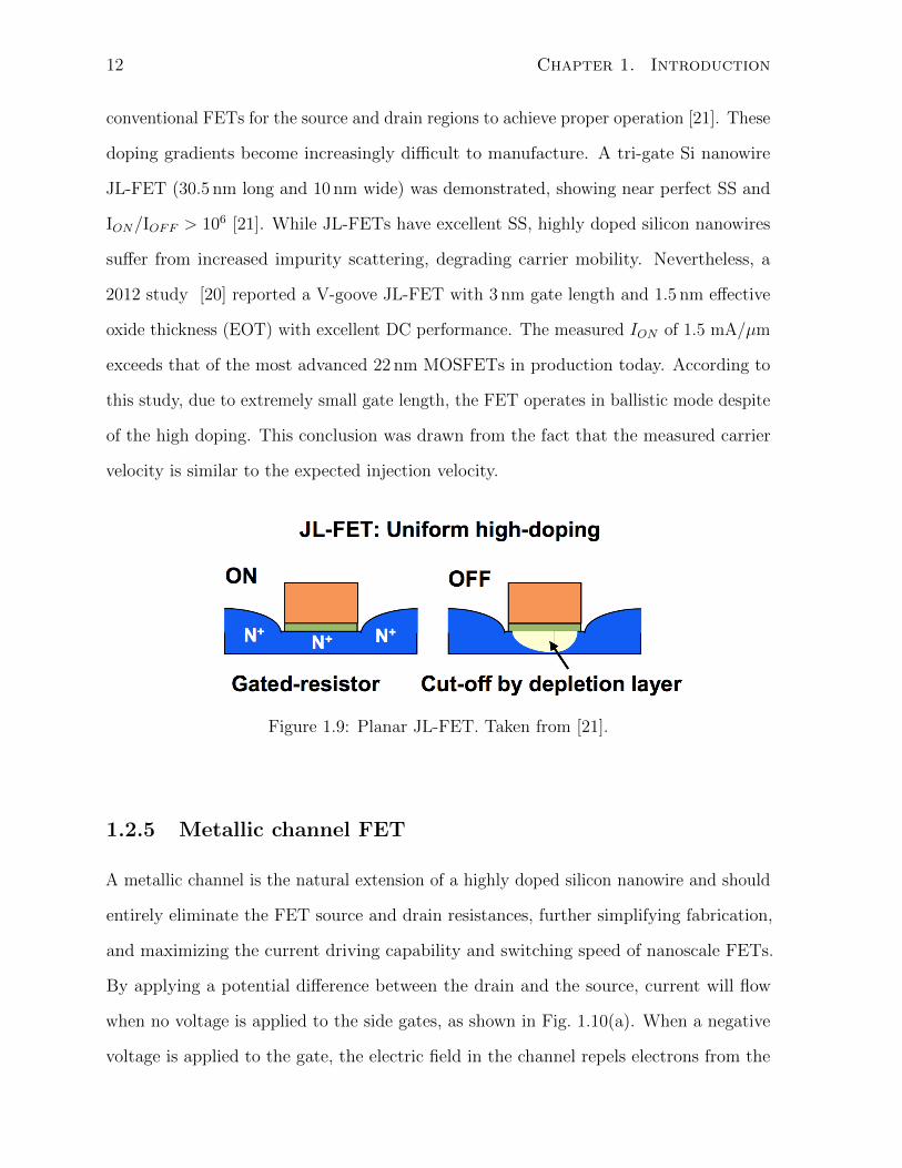
When a graphene sheet is rolled onto itself into a tube, it forms a carbon nanotube
(CNT), a one-dimensional (1D) cylindrical crystal whose bandgap is determined by the
diamater of the tube. In general, carbon nanotube FETs (CNTFETs) suffer from the
same problems as graphene FETs. However, recently a new technique was developed to
manufacture high-mobility gate-all-around CNTFETs by suspending the CNT in air by
etching the silicon substrate underneath. As shown in Figure 1.8, the CNT retains most
1.2. Device candidates beyond CMOS 11
of its intrinsic carrier mobility [17]. The FET in [17] exhibits very good ION exceeding
that of the most advanced 30 nm InP High-Electron-Mobility Transistors (HEMTs) which
currently hold the record for the highest fT and fMAX transistors.
(a) CNT suspended in air(b) GAA CNTFET
(c) I-V Characteristics
Figure 1.8: Fully self-aligned GAA CNTFET. Taken from [17].
1.2.4 Junctionless FET
The concept of a junctionless FET (JL-FET) dates back to the first FET patent submitted
by Lilienfeld in 1926 [18]. S. V. Rotkin and K. Hess recently revisited the concept, applying
it to multi-walled metallic CNTs [19]. A JL-FET is regarded as a ”gated-resistor” whose
main feature is the absence of PN junctions at the source and drain regions [20]. The
source, drain, and channel are highly-doped with the same type of dopant. Current flow
is controlled by the formation of a depletion layer in the channel induced by the gate
voltage. Because of the high doping (> 1018 cm−3) in the source, channel, and drain,
the semiconductor is almost metallic in nature. The advantages of the JL-FET become
apparent below 10 nm gate length to avoid the ultra-high doping gradients necessary in
12 Chapter 1. Introduction
conventional FETs for the source and drain regions to achieve proper operation [21]. These
doping gradients become increasingly difficult to manufacture. A tri-gate Si nanowire
JL-FET (30.5 nm long and 10 nm wide) was demonstrated, showing near perfect SS and
ION/IOFF > 106 [21]. While JL-FETs have excellent SS, highly doped silicon nanowires
suffer from increased impurity scattering, degrading carrier mobility. Nevertheless, a
2012 study [20] reported a V-goove JL-FET with 3 nm gate length and 1.5 nm effective
oxide thickness (EOT) with excellent DC performance. The measured ION of 1.5 mA/µm
exceeds that of the most advanced 22 nm MOSFETs in production today. According to
this study, due to extremely small gate length, the FET operates in ballistic mode despite
of the high doping. This conclusion was drawn from the fact that the measured carrier
velocity is similar to the expected injection velocity.
Figure 1.9: Planar JL-FET. Taken from [21].
1.2.5 Metallic channel FET
A metallic channel is the natural extension of a highly doped silicon nanowire and should
entirely eliminate the FET source and drain resistances, further simplifying fabrication,
and maximizing the current driving capability and switching speed of nanoscale FETs.
By applying a potential difference between the drain and the source, current will flow
when no voltage is applied to the side gates, as shown in Fig. 1.10(a). When a negative
voltage is applied to the gate, the electric field in the channel repels electrons from the
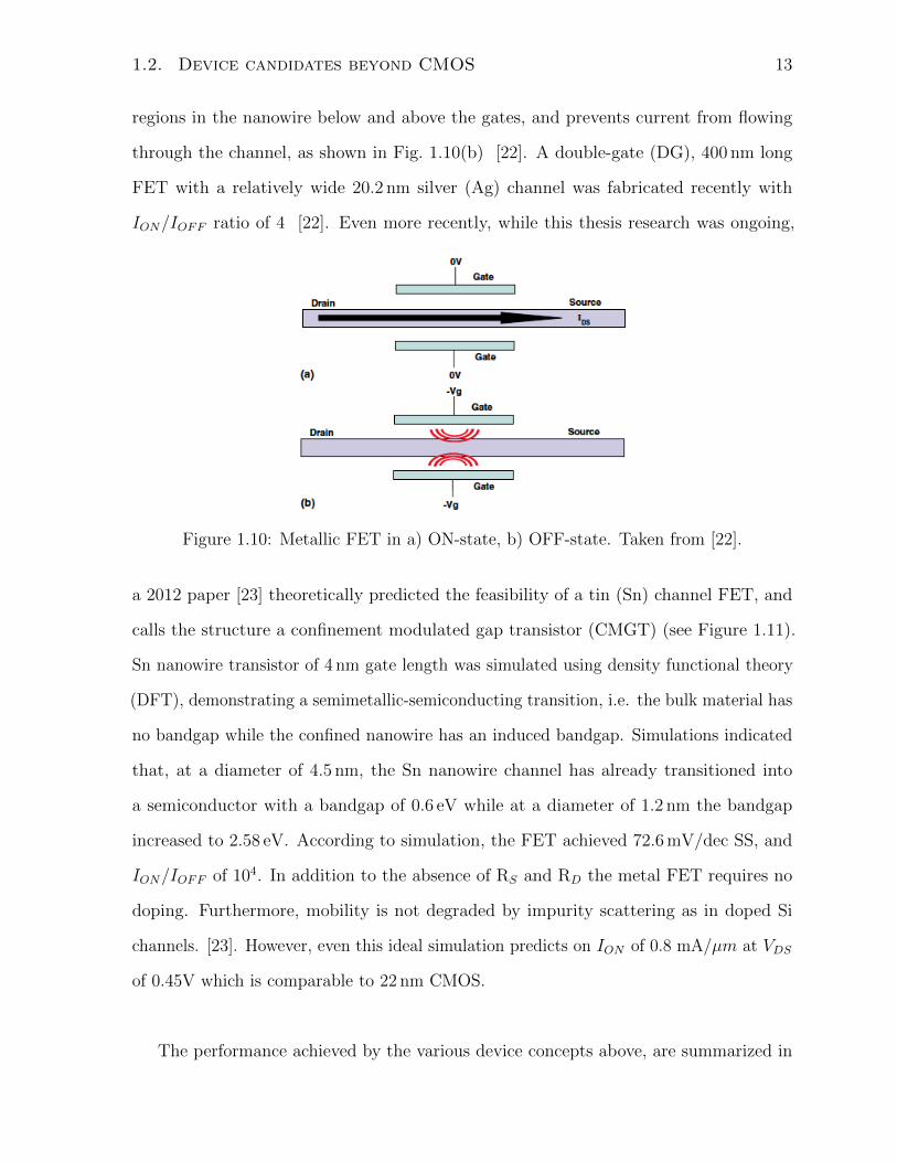
1.2. Device candidates beyond CMOS 13
regions in the nanowire below and above the gates, and prevents current from flowing
through the channel, as shown in Fig. 1.10(b) [22]. A double-gate (DG), 400 nm long
FET with a relatively wide 20.2 nm silver (Ag) channel was fabricated recently with
ION/IOFF ratio of 4 [22]. Even more recently, while this thesis research was ongoing,
Figure 1.10: Metallic FET in a) ON-state, b) OFF-state. Taken from [22].
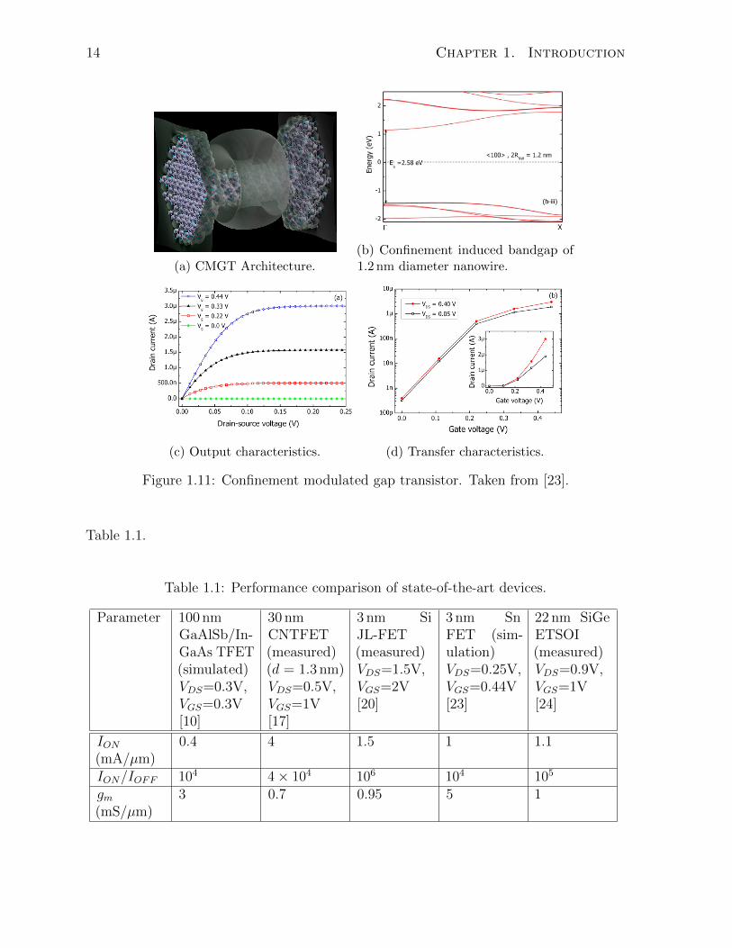
a 2012 paper [23] theoretically predicted the feasibility of a tin (Sn) channel FET, and
calls the structure a confinement modulated gap transistor (CMGT) (see Figure 1.11).
Sn nanowire transistor of 4 nm gate length was simulated using density functional theory
(DFT), demonstrating a semimetallic-semiconducting transition, i.e. the bulk material has
no bandgap while the confined nanowire has an induced bandgap. Simulations indicated
that, at a diameter of 4.5 nm, the Sn nanowire channel has already transitioned into
a semiconductor with a bandgap of 0.6 eV while at a diameter of 1.2 nm the bandgap
increased to 2.58 eV. According to simulation, the FET achieved 72.6 mV/dec SS, and
ION/IOFF of 104. In addition to the absence of RS and RD the metal FET requires no
doping. Furthermore, mobility is not degraded by impurity scattering as in doped Si
channels. [23]. However, even this ideal simulation predicts on ION of 0.8 mA/µm at VDS
of 0.45V which is comparable to 22 nm CMOS.
The performance achieved by the various device concepts above, are summarized in
14 Chapter 1. Introduction
(a) CMGT Architecture.(b) Confinement induced bandgap of1.2 nm diameter nanowire.
(c) Output characteristics. (d) Transfer characteristics.
Figure 1.11: Confinement modulated gap transistor. Taken from [23].
Table 1.1.
Table 1.1: Performance comparison of state-of-the-art devices.
Parameter 100 nmGaAlSb/In-GaAs TFET(simulated)VDS=0.3V,VGS=0.3V[10]
30 nmCNTFET(measured)(d = 1.3 nm)VDS=0.5V,VGS=1V[17]
3 nm SiJL-FET(measured)VDS=1.5V,VGS=2V[20]
3 nm SnFET (sim-ulation)VDS=0.25V,VGS=0.44V[23]
22 nm SiGeETSOI(measured)VDS=0.9V,VGS=1V[24]
ION(mA/µm)
0.4 4 1.5 1 1.1
ION/IOFF 104 4× 10⁴ 106 104 105
gm(mS/µm)
3 0.7 0.95 5 1
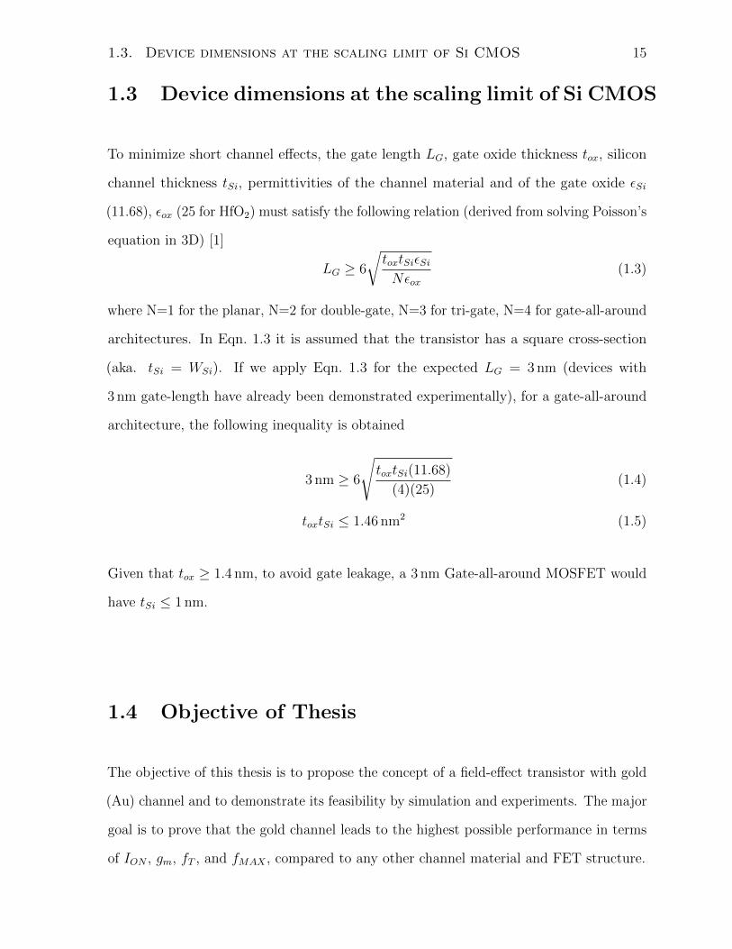
1.3. Device dimensions at the scaling limit of Si CMOS 15
1.3 Device dimensions at the scaling limit of Si CMOS
To minimize short channel effects, the gate length LG, gate oxide thickness tox, silicon
channel thickness tSi, permittivities of the channel material and of the gate oxide εSi
(11.68), εox (25 for HfO2) must satisfy the following relation (derived from solving Poisson’s
equation in 3D) [1]
LG ≥ 6
√toxtSiεSiNεox
(1.3)
where N=1 for the planar, N=2 for double-gate, N=3 for tri-gate, N=4 for gate-all-around
architectures. In Eqn. 1.3 it is assumed that the transistor has a square cross-section
(aka. tSi = WSi). If we apply Eqn. 1.3 for the expected LG = 3 nm (devices with
3 nm gate-length have already been demonstrated experimentally), for a gate-all-around
architecture, the following inequality is obtained
3 nm ≥ 6
√toxtSi(11.68)
(4)(25)(1.4)
toxtSi ≤ 1.46 nm2 (1.5)
Given that tox ≥ 1.4 nm, to avoid gate leakage, a 3 nm Gate-all-around MOSFET would
have tSi ≤ 1 nm.
1.4 Objective of Thesis
The objective of this thesis is to propose the concept of a field-effect transistor with gold
(Au) channel and to demonstrate its feasibility by simulation and experiments. The major
goal is to prove that the gold channel leads to the highest possible performance in terms
of ION , gm, fT , and fMAX , compared to any other channel material and FET structure.
16 Chapter 1. Introduction
1.5 Thesis Outline
The thesis is organized as follows. Chapter 2 introduces the theoretical background
necessary to understand the operation of nano-scale devices. Chapter 3 describes the
numerical methods used to predict and evaluate device performance. In Chapter 4, the
proposed device structure is introduced. Chapter 5 describes the simulation results and
the characterization of the proposed FET. Chapter 6 proposes a simple fabrication flow
and discusses initial feasibility experiments. Finally, Chapter 7 provides conclusions and
a discussion of further research efforts.
Chapter 2
Theoretical Background
This chapter presents the theoretical concepts for analysis of nano-electronic devices. The
major topics discussed are:
Bandstructure and Density of States Material properties begin to change when
scaled to extremely small dimensions on the order of few atomic lengths. Thus,
must be accounted for in the design of the next generation of electronic devices.
Schrodinger equation must be solved to determine the bandstructure and density of
states in the device.
Carrier transport Due to the lateral scaling of MOSFETs below 10 nm, the drift-
diffusion equation can no longer accurately describe carrier transport. Ballistic
transport must be accounted for in the carrier tranport equations.
2.1 Schrodinger equation
The quantum state of physical systems is determined by solving the time-independent
Schrodinger equation [25]:
Hψ = Eψ (2.1)
17
18 Chapter 2. Theoretical Background
where H is the Hamiltonian operator (or simply Hamiltonian), ψ is the particle wavefunc-
tion, and E is an energy eigenvalue of H. A solution of the time-independent equation is
called an energy eigenstate with energy E [25]. The Hamiltonian defines the total energy
of a system through summation of the kinetic and the potential energies as
H =−~2
2m∇2 + U(r) (2.2)
where ~ is the reduced Planck constant, m is the mass of the particle, and U(r) is the
potential energy [eV]. When an electron is confined to a periodic potential U(r) = U(r+R),
such as an infinite crystal lattice, the particle wavefunction may be expressed as the
product of a plane wave envelope function and a periodic function unk(r) that has the
same periodicity as the potential [25]
ψnk(r) = eik·runk(r) (2.3)
This is known as Bloch’s theorem. The corresponding energy eigenvalues are En(k) =
En(k + K), periodic with periodicity K of a reciprocal lattice vector. The energies
associated with the index n vary continuously with wave vector k and form an energy
band identified by band index n. The eigenvalues for given n are periodic in k; all distinct
values of En(k) occur for k-values within the first Brillouin zone of the reciprocal lattice
[25]. The collection of energy eigenstates within the first Brillouin zone is called the
bandstructure. All the properties of electrons in a periodic potential can be calculated
from this bandstructure and the associated wavefunctions.
2.2 Bandstructure and Density of States
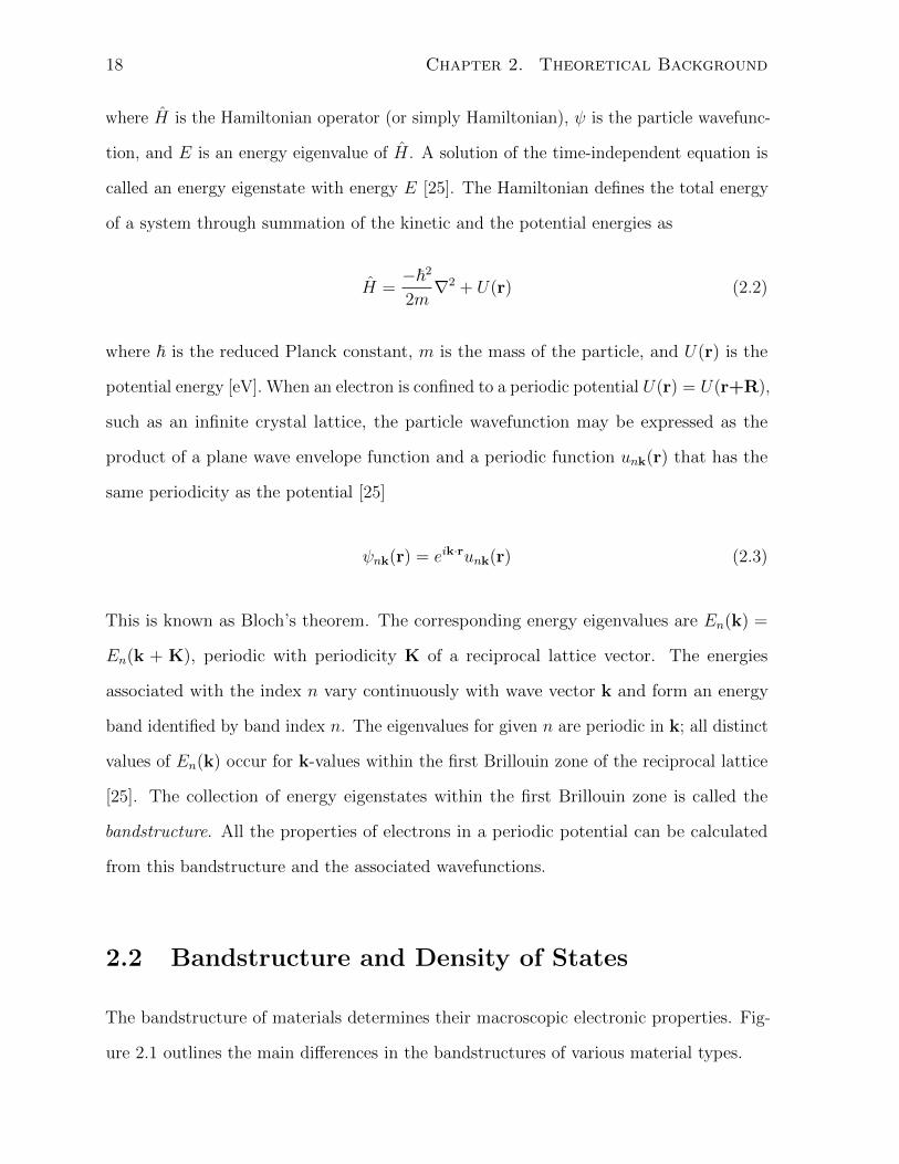
The bandstructure of materials determines their macroscopic electronic properties. Fig-
ure 2.1 outlines the main differences in the bandstructures of various material types.
2.2. Bandstructure and Density of States 19
Figure 2.1: Differences between metals, semiconductors, and insulators.
The Fermi level (EF ) defines the energy level below which all states are occupied by
electrons and above which no states are occupied. The Fermi-Dirac probability function
gives the probability of occupancy of an energy level E, as
f(E) =1
1 + e(E−EF )/ kBT(2.4)
In insulators and semiconductors, the Fermi level is located near the center of the
bandgap (energy range with no energy eigenstates) formed between the valence band
(energy band of the valence electrons) and conduction band (energy band where electrons
can move around freely). In the case of insulators, the bandgap is too broad (> 4 eV) and,
at room temperature, no thermal excitation can energize an electron to jump in the con-
duction band. In semiconductors, the bandgap is smaller than in insulators (0.2-4 eV) and
at room temperature there are few atoms that ionize and create free electrons (1010 cm−3
for intrinsic Si) [3]. We may introduce impurities in the crystal that shift the Fermi level
towards/away from the conduction band to create n-type and p-type semiconductors. In
the case of metals, the Fermi level is located in the conduction band. Thus, there is a
considerable concentration of free electrons in the intrinsic material (1021 cm−3) available
20 Chapter 2. Theoretical Background
for conduction [3]. This is the general view of three dimensional (3D) or bulk materials.
However, the principle of bandstructure can only be defined to an infinite periodic solid
[3]. For devices with a small number of atoms (<10,000) the bandstructure begins to
deviate from its assumed infinite periodic solid band calculation.
Since the isolation and proof of existence of the two dimensional (2D) crystal graphene
in 2004, many groups around the world have been working on identifying other 2D crystals.
In recent years, several other 2D materials have attracted research interest, namely, MoS2,
WS2, BN, and even more recently, silicene and germanene. There seems to be a trend that
the bulk form of such materials (excluding silicene and germanene) is used in lubricants
where sheets of the materials are weakly bonded by van Der Waals forces and can slide
off or peel off easily. On the other hand, silicene and germanene are artificial derivatives
of their natural 3D form. There is now overwhelming experimental evidence that the
bandstructure changes as the dimensions of the materials reduce from 3D to 2D or 1D.
For instance, if graphite is confined into a two dimensional sheet (graphene), the shape
of the conduction band is significantly changed to form a Dirac cone. This translates
into electrons in graphene acting as massless Dirac fermions with zero mass and superior
mobility, which makes a significant deviation from graphite’s 3D properies. Moreover, if a
graphene sheet is narrow (< 20 nm), the edges of the structure become so significant that
depending on the type of edge (armchair or zigzag) one may create a semiconducting
material with a bandgap or a metallic material with no bandgap. In such materials,
dopants may be introduced by passivating the edge atoms with either hydrogen or flourine.
The density of states (DOS) of a system describes the number of states per interval of
energy at each energy level that are available to be occupied by electrons. The general
formula for calculating DOS is
D(E) =∑k
δ(E − E(k)) (2.5)
2.2. Bandstructure and Density of States 21
where the D(E) [eV−1] is expressed as the summation of Dirac delta δ(E) functions
corresponding to allowed energy levels by the E(k) relationship of the crystal. When
there are lots of states, they interact with each other causing a broadening, and the
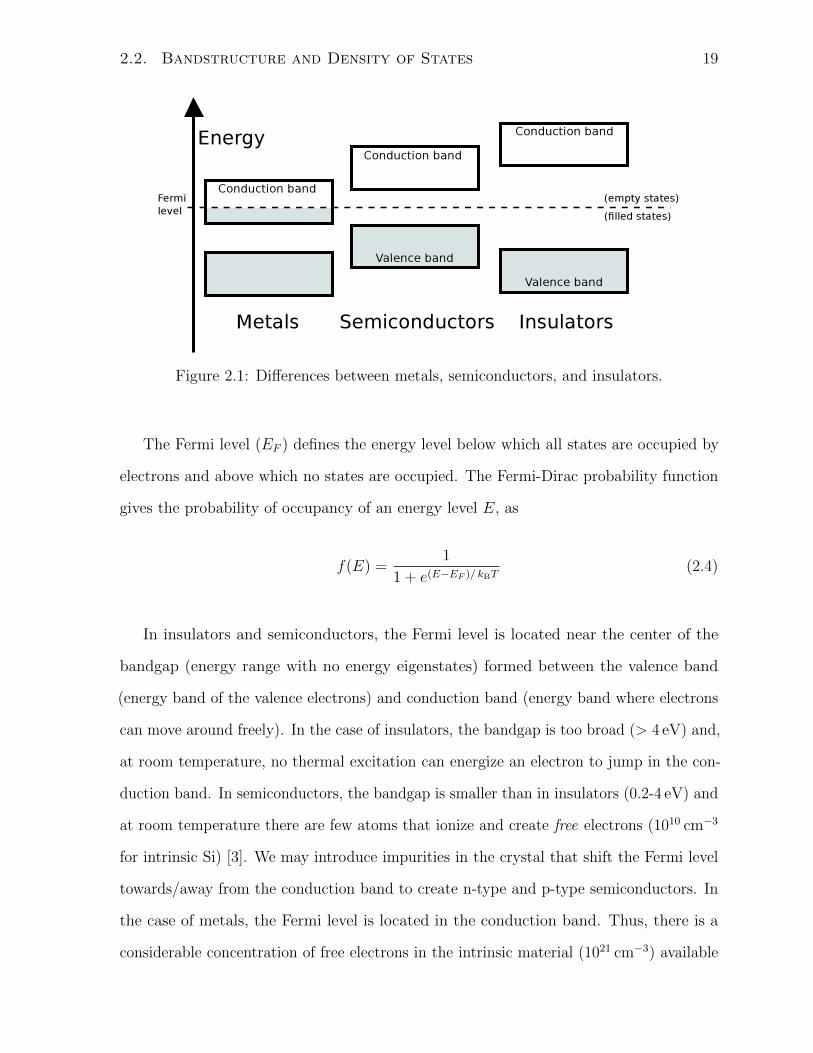
D(E) can be approximated by a smooth curve. Such is the case for DOS in a typical 3D
semiconductor as illustrated in Figure 2.2. The forbidden gap contains no states (thus
DOS in the gap is zero), while the energy bands contain many states.
Figure 2.2: Bandstructure (left) and DOS (right) of a typical semiconductor.
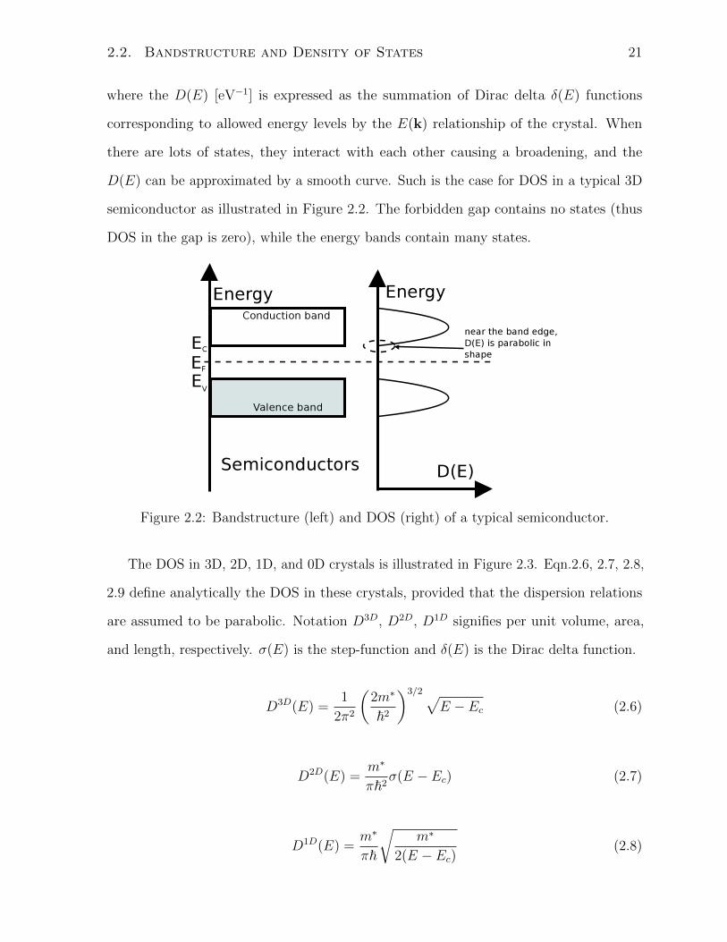
The DOS in 3D, 2D, 1D, and 0D crystals is illustrated in Figure 2.3. Eqn.2.6, 2.7, 2.8,
2.9 define analytically the DOS in these crystals, provided that the dispersion relations
are assumed to be parabolic. Notation D3D, D2D, D1D signifies per unit volume, area,
and length, respectively. σ(E) is the step-function and δ(E) is the Dirac delta function.
D3D(E) =1
2π2
(2m∗
~2
)3/2√E − Ec (2.6)
D2D(E) =m∗
π~2σ(E − Ec) (2.7)
D1D(E) =m∗
π~
√m∗
2(E − Ec)(2.8)
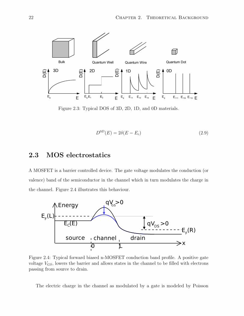
22 Chapter 2. Theoretical Background
Figure 2.3: Typical DOS of 3D, 2D, 1D, and 0D materials.
D0D(E) = 2δ(E − Ec) (2.9)
2.3 MOS electrostatics
A MOSFET is a barrier controlled device. The gate voltage modulates the conduction (or
valence) band of the semiconductor in the channel which in turn modulates the charge in
the channel. Figure 2.4 illustrates this behaviour.
Figure 2.4: Typical forward biased n-MOSFET conduction band profile. A positive gatevoltage VGS, lowers the barrier and allows states in the channel to be filled with electronspassing from source to drain.
The electric charge in the channel as modulated by a gate is modeled by Poisson
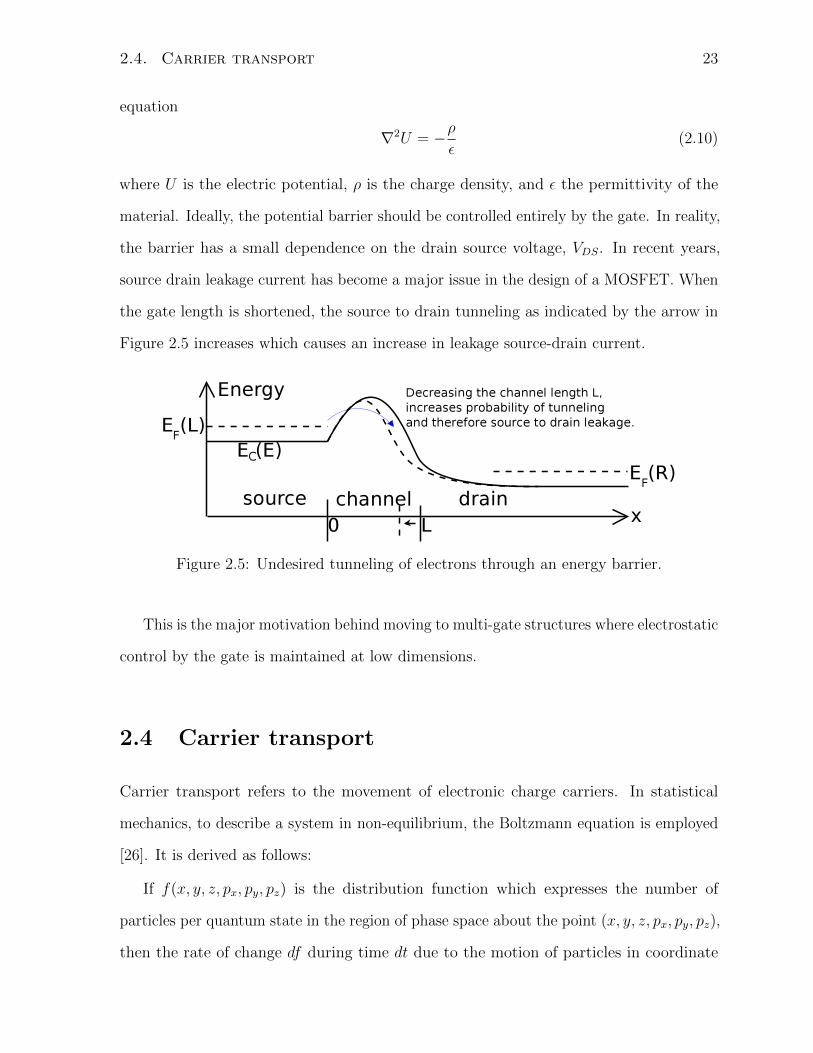
2.4. Carrier transport 23
equation
∇2U = −ρε
(2.10)
where U is the electric potential, ρ is the charge density, and ε the permittivity of the
material. Ideally, the potential barrier should be controlled entirely by the gate. In reality,
the barrier has a small dependence on the drain source voltage, VDS. In recent years,
source drain leakage current has become a major issue in the design of a MOSFET. When
the gate length is shortened, the source to drain tunneling as indicated by the arrow in
Figure 2.5 increases which causes an increase in leakage source-drain current.
Figure 2.5: Undesired tunneling of electrons through an energy barrier.
This is the major motivation behind moving to multi-gate structures where electrostatic
control by the gate is maintained at low dimensions.
2.4 Carrier transport
Carrier transport refers to the movement of electronic charge carriers. In statistical
mechanics, to describe a system in non-equilibrium, the Boltzmann equation is employed
[26]. It is derived as follows:
If f(x, y, z, px, py, pz) is the distribution function which expresses the number of
particles per quantum state in the region of phase space about the point (x, y, z, px, py, pz),
then the rate of change df during time dt due to the motion of particles in coordinate
24 Chapter 2. Theoretical Background
space under the influence of a force field F, where F = dp/dt, in momentum space is [26]
df = f(x− vxdt, y − vydt, z − vzdt, px − Fxdt, py − Fydt, pz − Fzdt)− f(x, y, z, px, py, pz)
(2.11)
then using Taylor series expansion, and retaining only first-order terms, the rate of change
over time is expressed as
df
dt= −v · ∇f − F · ∇pf (2.12)
where v is the velocity of the particles, and∇p refers to the gradient operator in momentum
space. Particles may also be transferred into and out of a region by collisions [26]. If the
rate of change of the distribution function due to collisions is denoted by (df/dt)coll, then
the total rate of change of f is obtained
df
dt= −v · ∇f − F · ∇pf +
(df
dt
)coll
(2.13)
This is the Boltzmann equation [26]. The choice of statistical distribution function f used
in the equation accounted for various phenomenon.
2.4.1 Drift-diffusion
The Boltzmann equation can be solved in order to obtain a simplified expression for
current using Boltzmann statistics. Assuming that free charge carriers in a uniform
conducting sheet do a random walk under a small applied bias (see Figure 2.6), charges
”drift” at an average velocity υd. The average distance between scattering events is called
the mean free path, denoted by λ. The average time that the charge travels before it
scatters is called the mean free time, denoted by τ . The ”drift” current density Jdrift
[A/cm2] in the device under small applied electric field E , is
Jdrift = I/W = nsqµnE (2.14)
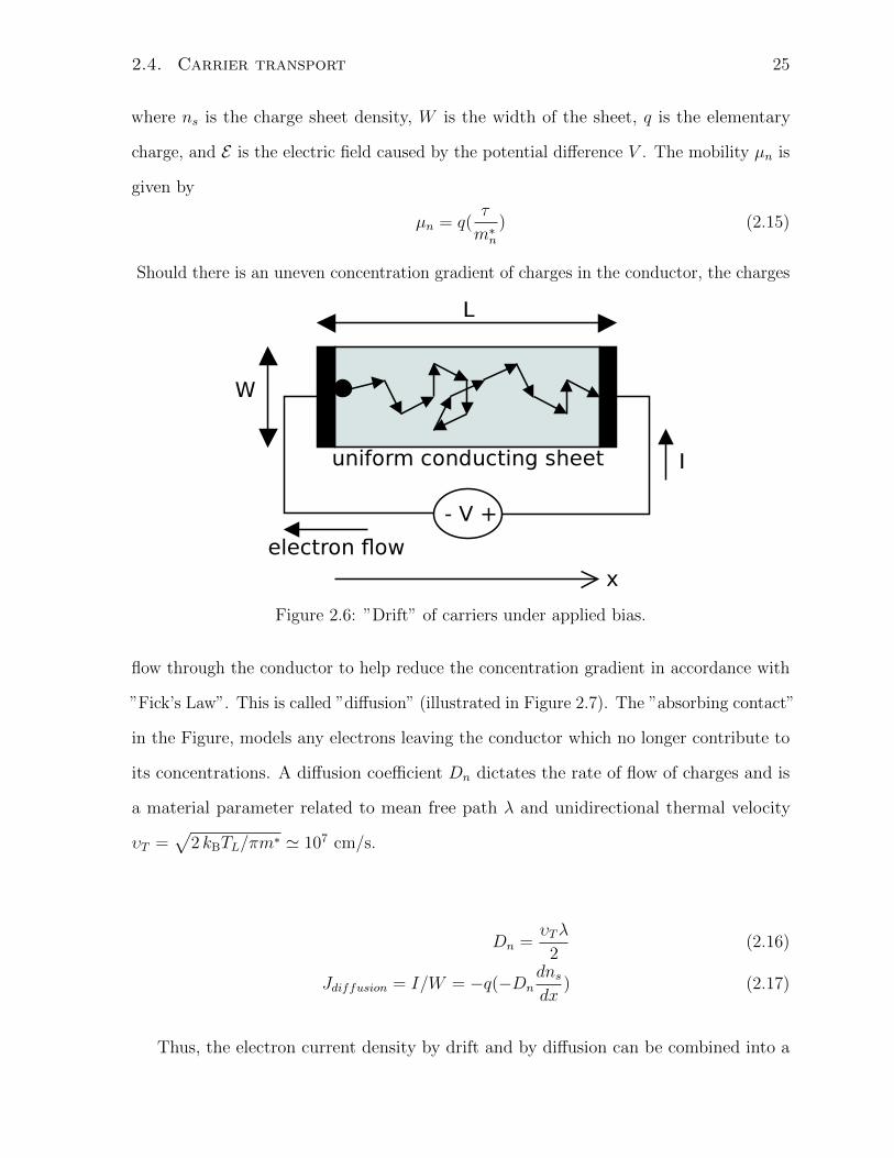
2.4. Carrier transport 25
where ns is the charge sheet density, W is the width of the sheet, q is the elementary
charge, and E is the electric field caused by the potential difference V . The mobility µn is
given by
µn = q(τ
m∗n) (2.15)
Should there is an uneven concentration gradient of charges in the conductor, the charges
Figure 2.6: ”Drift” of carriers under applied bias.
flow through the conductor to help reduce the concentration gradient in accordance with
”Fick’s Law”. This is called ”diffusion” (illustrated in Figure 2.7). The ”absorbing contact”
in the Figure, models any electrons leaving the conductor which no longer contribute to
its concentrations. A diffusion coefficient Dn dictates the rate of flow of charges and is
a material parameter related to mean free path λ and unidirectional thermal velocity
υT =√
2 kBTL/πm∗ ' 107 cm/s.
Dn =υTλ
2(2.16)
Jdiffusion = I/W = −q(−Dndnsdx
) (2.17)
Thus, the electron current density by drift and by diffusion can be combined into a
26 Chapter 2. Theoretical Background
Figure 2.7: Diffusion of carriers from left to right due to a concentration gradient.
”drift-diffusion” equation:
Jn = nsqµnE + qDndnsdx
(2.18)
The mobility and diffusion coefficient are related through the ”Einstein relation”
(assuming Boltzmann statistics) in the following manner:
Dn
µn=
kBT
q(2.19)
Table 2.1: Mobility of common semiconductor materials.
Table 2.1 shows the mobilities of common semiconductor materials. Materials with
2.4. Carrier transport 27
lower bandgap tend to have higher electron mobility. However, too narrow a bandgap
leads to high leakage current and low breakdown voltage.
2.4.2 Ballistic transport
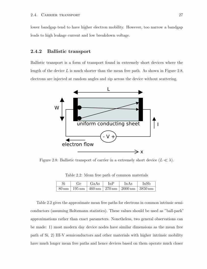
Ballistic transport is a form of transport found in extremely short devices where the
length of the device L is much shorter than the mean free path. As shown in Figure 2.8,
electrons are injected at random angles and zip across the device without scattering.
Figure 2.8: Ballistic transport of carrier in a extremely short device (L λ).
Table 2.2: Mean free path of common materials
Si Ge GaAs InP InAs InSb80 nm 195 nm 460 nm 270 nm 2000 nm 3850 nm
Table 2.2 gives the approximate mean free paths for electrons in common intrinsic semi-
conductors (assuming Boltzmann statistics). These values should be used as ”ball-park”
approximations rather than exact parameters. Nonetheless, two general observations can
be made: 1) most modern day device nodes have similar dimensions as the mean free
path of Si, 2) III-V semiconductors and other materials with higher intrinsic mobility
have much longer mean free paths and hence devices based on them operate much closer
28 Chapter 2. Theoretical Background
to ballistic limit than silicon. Note that, when dopants are introduced in a semiconductor,
they degrade the intrinsic mobility and shorten the mean free path.
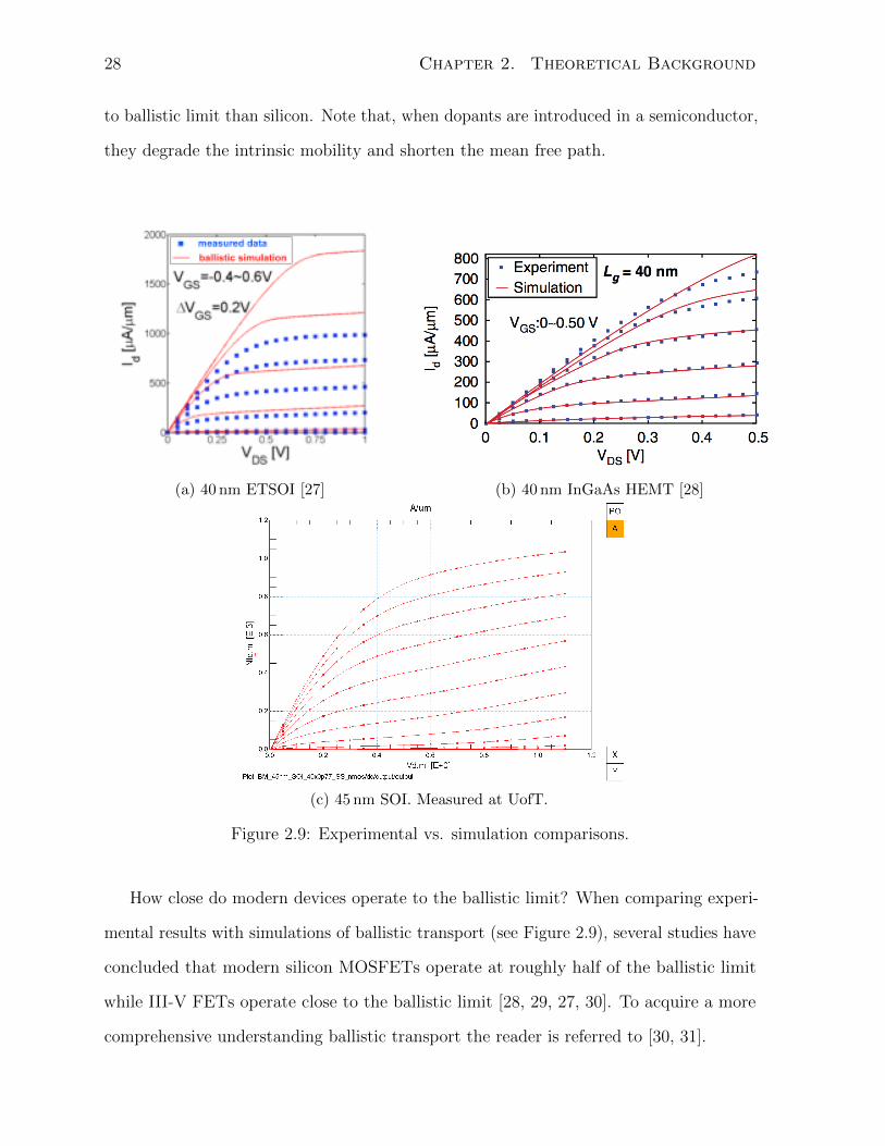
(a) 40 nm ETSOI [27] (b) 40 nm InGaAs HEMT [28]
(c) 45 nm SOI. Measured at UofT.
Figure 2.9: Experimental vs. simulation comparisons.
How close do modern devices operate to the ballistic limit? When comparing experi-
mental results with simulations of ballistic transport (see Figure 2.9), several studies have
concluded that modern silicon MOSFETs operate at roughly half of the ballistic limit
while III-V FETs operate close to the ballistic limit [28, 29, 27, 30]. To acquire a more
comprehensive understanding ballistic transport the reader is referred to [30, 31].
2.4. Carrier transport 29
In the ballistic MOSFET, electrons populate discrete subbands with a minimum energy
Ej (jth subband) above the conduction band E ′C [3]. The probability of occupancy of
each state is given by the Fermi-Dirac distribution function. The charge density per unit
area of the electrons moving from source to drain is modeled by [3]
dQj+ =(2g/h2)qmymzdνydνz
1 + e(E′C+Ej+myν2y/2+mzν2z/2−EF (S))/ kBT
(2.20)
where my, and mz are the masses of electrons in the y and z directions, νy, νz are the
velocities of electrons in the y and z directions, and g is the degeneracy number. The
current per width is given by the product of charge density and carrier velocity summed
over all subbands:
I+ = W∑j
∫allνz
∫νy>0
νydQj+ (2.21)
This integral can be determined analytically by a change of variable u = ν2y . Using
integration by parts, the result of the second integral is expressed in terms of Fermi-Dirac
integral:
F1/2(u) =
∫ ∞0
√ydy
1 + ey−u(2.22)
And the current is given by
I+ =∑j
(4g/h2)qW√
2mz( kBT )3/2F1/2
(EF (S)− E ′C − EjkBT
)(2.23)
Similarly, the electrons moving from the drain to the source define a negative current
component I− [3]
I− =∑j
(4g/h2)qW√
2mz( kBT )3/2F1/2
(EF (D)− E ′C − EjkBT
)(2.24)
30 Chapter 2. Theoretical Background
The total current is the sum of the two components, IDS = I+ − I− and equal to
IDS =4√
2qW ( kBT )3/2
h2
(g√mz
∑j
[F1/2
(EF (S)− E ′C − EjkBT
)− F1/2
(EF (S)− qVDS − E ′C − EjkBT
)](2.25)
+g′√m′z∑j
[F1/2
(EF (S)− E ′C − Ej′
kBT
)− F1/2
(EF (S)− qVDS − E ′C − Ej′
kBT
)])(2.26)
The unknowns EF (S)−E ′C−Ej and EF (S)−E ′C−Ej′ are controlled by the gate voltage
and must be solved numerically from the coupled Poisson’s and Schrodinger’s equations
[3]. Spin degeneracy g, and effective mass mz in the direction perpendicular to current
flow is material and orientation dependent.
2.5 Landauer approach to Carrier Transport
The study of devices which inherently employ quantum-mechanical effects in their opera-
tion require treatment on a more fundamental level starting with Schrodinger equation
[31]. The simplest model of quantum transport in devices is to describe the problem
in terms of scattering of the electron wavefunctions by a spatially varying potential
[31]. It is assumed that this potential is situated between two electron reservoirs which
emit particles in the central, scattering, region. The net flux of electrons between the
reservoirs constitutes the electric current. The incident to transmitted flux ratio is called
the transmission probability, T , and expressed as
T =vrvl|tr|2 =
vlvr|tl|2 (2.27)
where v = (1/~)dE/dk is the electron velocity, and tr, tl are transmission amplitudes of
the solutions to the one-dimensional Schrodinger equation.
2.5. Landauer approach to Carrier Transport 31
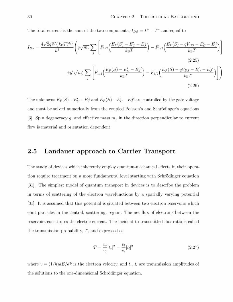
The reservoirs can have different Fermi levels EF (L) and EF (R), where their difference
represents an applied bias voltage. Figure 2.10 depicts the model. D(E) is the density of
states in the central region.
x
D(E)
central region, device
qVDS
E (L)F
E (R)F
f (E)1
f (E)2
I
Figure 2.10: Representation of a nano-scale device where the electrodes are modelled aselectron ”reservoirs” with Fermi distribution functions f1 and f2 and the density of statesrepresents the central region.
The assumptions made are [32]:
1. The central region is described by its D(E)
2. Contacts are large with strong inelastic scattering, always near equilibrium
3. Contacts ”absorb” electrons.
4. Electrons flow in independent energy channels
In steady state, near-equilibrium, the current through the central region is [32]
I =2q
h
∫T (E)M(E)(f1 − f2)dE (2.28)
where T (E) is the transmission probability as a function of energy, M(E) is the density
of modes, f1 and f2 are the Fermi functions of the contact regions. T (E) is a function
with values in the interval [0,1] which describes the probability that an electron will pass
through without being scattered at a given energy level. M(E) indicates the number of
independent channels that electrons use and is equal to M(E) = πγD(E) where γ is a
32 Chapter 2. Theoretical Background
coupling coefficient as to how fast electrons can get in and out of the central region [32].
Landauer, derived that for a small applied bias VDS, the difference of Fermi functions can
be linearized and the current expressed as a function of voltage where G is the conductance
I =
(2q2
h
∫T (E)M(E)(−df0/dE)dE
)VDS = GVDS (2.29)
The factor of 2 is due to spin degeneracy, the constant q2/h is known as ”quantum of
conductance” and is equal to 39.6µS. Its inverse is 25.2kΩ [31]. This result has been
experimentally verified in GaAs at room temperature and various systems at 4K. For a
more elaborate explanation, the reader is referred to [32].
Near-equilibrium transport of a quantum device can be described by invoking the
Landauer conductance formula [31]. However, far-from-equilibrium transport, where most
useful devices operate, must be described in terms of quantum statistical mechanics.
The Boltzmann equation cannot properly deal with quantum interference effects. More
comprehensive theories have been developed such as the use of Wigner distribution
function in the Boltzmann equation and non-equilibrium Green’s function formalism.
There is no one theoretical tool that provides a complete model of quantum device
behaviour [31].
Chapter 3
Simulation of nano-scale devices
3.1 Non-equilibrium Green’s function (NEGF) for-
malism
In the NEGF formalism, a device is treated as having right and left ”electrode” regions
and a central region. The right and left electrodes are modeled by their Fermi levels EF (L)
and EF (R), respectively. These potentials are commonly set such that they represent the
”bulk” Fermi level of the material used. When a voltage VDS is applied between the two
electrodes, EF (L) and EF (R) are adjusted to satisfy
EF (R)− EF (L) = qVDS (3.1)
A representative figure for nano-scale device simulation is illustrated by Figure 3.1. In
the central region, the density of states is calculated using Schrodinger equation with the
Hamiltonian
H = − ~2m∇2 + V eff [ρ](r) (3.2)
33
34 Chapter 3. Simulation of nano-scale devices
Figure 3.1: Conceptual schematic of a nano-scale device simulation. The left and rightelectrodes are modeled as approximating the bulk properties of the material used inthem while the central region is modeled by its density of states D(E), dependent ondimensions, position x, and self-consistent effective potential V eff .
where the effective potential V eff is the sum of four potentials
V eff [ρ](r) = V H [ρ] + V xc[ρ] + V gate + ΣV pseudoµ (3.3)
V H [ρ] represents the Hartree potential (due to the electron density distribution and
ionic lattice), V xc[ρ] is an exchange-correlation potential, V gate is the potential due to
the voltage applied to the gate, and ΣV pseudoµ represents potentials caused by local and
non-local electron interaction. The summation of the occupied energies define the electron
density of the system given by
ρ(r) = Σ|ψ(r)|2f(E − EFkBT
) (3.4)
where f is the Fermi function. It is often more convenient to compare the electron density
with a superposition of atom based densities, ρatom(r−Rµ) where Rµ is the position of
atom µ,
∆ρ(r) = ρ(r)− Σρatom(r−Rµ) (3.5)
3.1. Non-equilibrium Green’s function (NEGF) formalism 35
This is known as the Electron difference density [33]. The solution is found through self-
consistent iteration between Schrodinger and Poisson equations. The complete algorithm
is:
1. Start with an initial guess for V eff (r)
2. For each eigen-energy, calculate G
G = [EI−H−Σ1 −Σ2]−1 (retarded Green’s function) (3.6)
A1 = GΓ1GH (spectral function) (3.7)
where Σ1, and Σ2 are the left and right self-energies (energies representing the
coupling of the central region to the left and right electrode ”reservoirs”), Γ1 is a
”broadening” function.
3. Determine the density matrix ρ1(x)
ρ1(r) =
∫2× dE
2πA1f(EF − E) (density matrix) (3.8)
4. Solve Poisson’s equation for V eff (r) based on ρ1(r). If V eff (r) is no longer varying
(aka. V eff (r)− V effold (r) < V eff
error(r)), the calculation is self-consistent, proceed to 5.
Otherwise, go to 2.
5. Calculate various properties of the system, such as transmission coefficient, and
current
T (E) = trace[Γ1GΓ2GH ] (3.9)
I =2q
h
∫T (E)[f(E − EF (R))− f(E − EF (L))]dE (current) (3.10)
The formula for current is identical to the one derived by Landauer Eqn. 2.28, where
36 Chapter 3. Simulation of nano-scale devices
the density of modes is absorbed by the transmission coefficient, T (E). For a more
elaborate discussion, the reader is referred to [32].
3.2 Simulation procedure and limitations
The algorithm outlined in Section 3.1 is implemented by Atomistix ToolKit v.12.8.0,
QuantumWise A/S. The definition of the device to be simulated can be broken down
into a series of steps outlined in Figure 3.2. The device is created from bulk material
by defining its dimensions, materials, composition, and material properties. Iteration
parameters are set to ensure numerical accuracy. Please refer to [34, 35, 36] for a more
detailed description of Atomistix. On a quad-core CPU with 8GB of RAM, devices
with up to 500 atoms may be simulated without compromising accuracy with runtimes
averaging from several hours to several days. Larger devices (1000 atoms and more)
require much more RAM and cannot be adequately modeled at this time. A fundamental
limitation of Atomistix is the far-from equilibrium bias with large current. Please refer
to limitations mentioned earlier in Section 2.5. It must be noted that this modelling
approach, generally underestimates the bandgap of materials. This is well documented in
literature and more information can be found here [37, 38, 39].
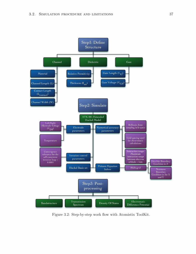
3.2. Simulation procedure and limitations 37
Step2: Simulate
ATK-SE: Extended Huckel Model
Electrode parameters
Left/Right Electrode Voltage
(VDS)
Iteration control parameters
Convergence tolerance for the self-consistent iteration loop =
0.0001
Numerical accuracy parameters
Grid spacing used for electrostatic
calculations
Interaction range: Maximum
interaction range between electron
orbitals = 1nm
Brillouin Zone sampling in k-space
Huckel Basis set
Temperature
Multi-gridNeumann Boundary
Condition in the X and Y
Dirichlet Boundary Condition in Z
Poisson Equation Solver
Step3: Post-processing
BandstructureTransmission
SpectrumDensity Of States
Electrostatic Difference Potential
Step1: Define Structure
Channel Dielectric
Relative Permitivity
Thickness (tox)
Gate
Gate Length (LG)
Gate Voltage (VGS)Channel Length (L)
Contact Length (Lcontact)
Channel Width (W)
Material
Figure 3.2: Step-by-step work flow with Atomistix ToolKit.
Chapter 4
Metallic FET
4.1 Proposed device structure
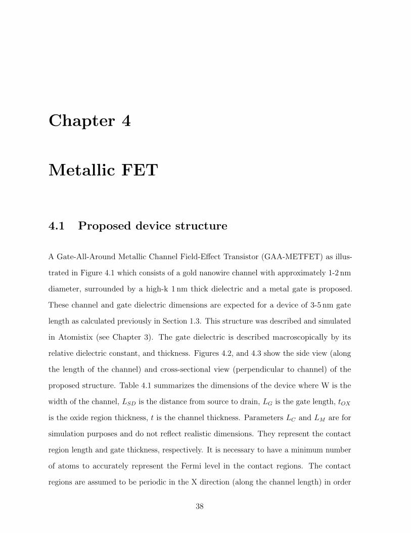
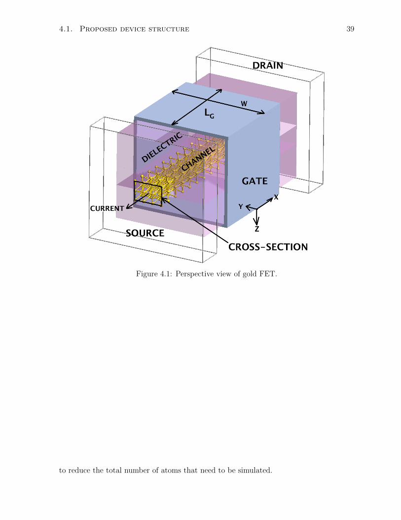
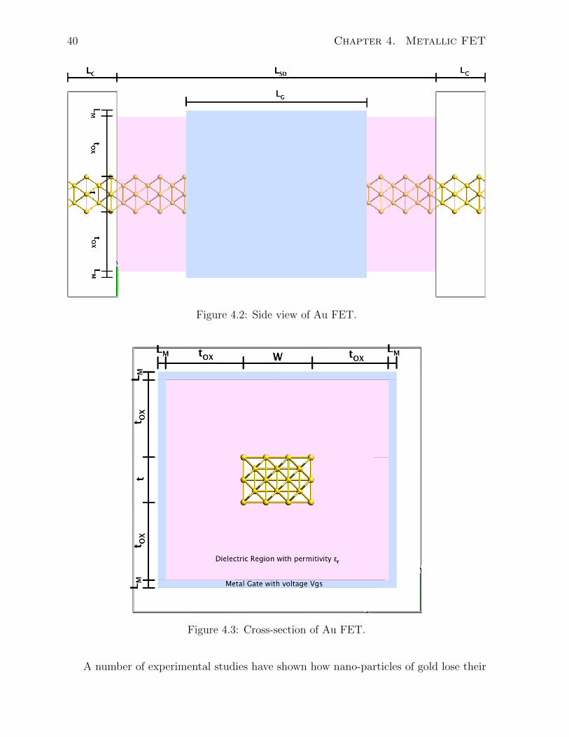
A Gate-All-Around Metallic Channel Field-Effect Transistor (GAA-METFET) as illus-
trated in Figure 4.1 which consists of a gold nanowire channel with approximately 1-2 nm
diameter, surrounded by a high-k 1 nm thick dielectric and a metal gate is proposed.
These channel and gate dielectric dimensions are expected for a device of 3-5 nm gate
length as calculated previously in Section 1.3. This structure was described and simulated
in Atomistix (see Chapter 3). The gate dielectric is described macroscopically by its
relative dielectric constant, and thickness. Figures 4.2, and 4.3 show the side view (along
the length of the channel) and cross-sectional view (perpendicular to channel) of the
proposed structure. Table 4.1 summarizes the dimensions of the device where W is the
width of the channel, LSD is the distance from source to drain, LG is the gate length, tOX
is the oxide region thickness, t is the channel thickness. Parameters LC and LM are for
simulation purposes and do not reflect realistic dimensions. They represent the contact
region length and gate thickness, respectively. It is necessary to have a minimum number
of atoms to accurately represent the Fermi level in the contact regions. The contact
regions are assumed to be periodic in the X direction (along the channel length) in order
38
4.1. Proposed device structure 39
Figure 4.1: Perspective view of gold FET.
to reduce the total number of atoms that need to be simulated.
40 Chapter 4. Metallic FET
Figure 4.2: Side view of Au FET.
Figure 4.3: Cross-section of Au FET.
A number of experimental studies have shown how nano-particles of gold lose their
4.1. Proposed device structure 41
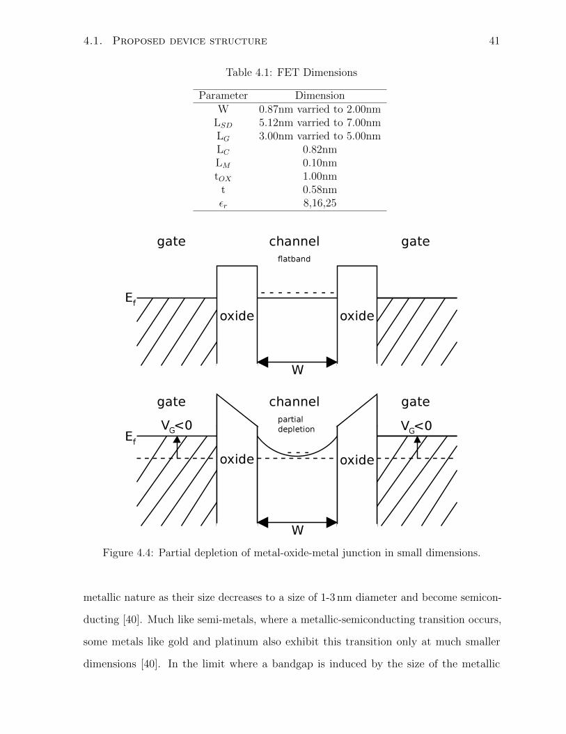
Table 4.1: FET Dimensions
Parameter DimensionW 0.87nm varried to 2.00nm
LSD 5.12nm varried to 7.00nmLG 3.00nm varried to 5.00nmLC 0.82nmLM 0.10nmtOX 1.00nm
t 0.58nmεr 8,16,25
Figure 4.4: Partial depletion of metal-oxide-metal junction in small dimensions.
metallic nature as their size decreases to a size of 1-3 nm diameter and become semicon-
ducting [40]. Much like semi-metals, where a metallic-semiconducting transition occurs,
some metals like gold and platinum also exhibit this transition only at much smaller
dimensions [40]. In the limit where a bandgap is induced by the size of the metallic
42 Chapter 4. Metallic FET
channel, the metallic channel can be treated as a semiconductor.
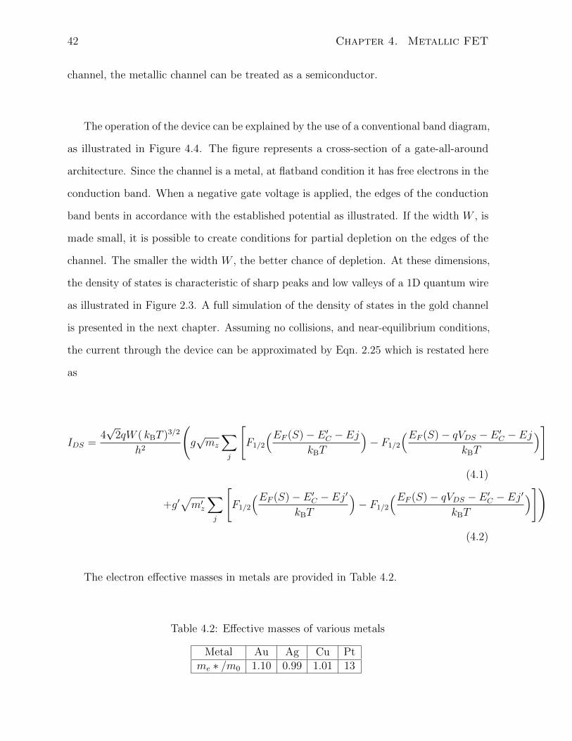
The operation of the device can be explained by the use of a conventional band diagram,
as illustrated in Figure 4.4. The figure represents a cross-section of a gate-all-around
architecture. Since the channel is a metal, at flatband condition it has free electrons in the
conduction band. When a negative gate voltage is applied, the edges of the conduction
band bents in accordance with the established potential as illustrated. If the width W , is
made small, it is possible to create conditions for partial depletion on the edges of the
channel. The smaller the width W , the better chance of depletion. At these dimensions,
the density of states is characteristic of sharp peaks and low valleys of a 1D quantum wire
as illustrated in Figure 2.3. A full simulation of the density of states in the gold channel
is presented in the next chapter. Assuming no collisions, and near-equilibrium conditions,
the current through the device can be approximated by Eqn. 2.25 which is restated here
as
IDS =4√
2qW ( kBT )3/2
h2
(g√mz
∑j
[F1/2
(EF (S)− E ′C − EjkBT
)− F1/2
(EF (S)− qVDS − E ′C − EjkBT
)](4.1)
+g′√m′z∑j
[F1/2
(EF (S)− E ′C − Ej′
kBT
)− F1/2
(EF (S)− qVDS − E ′C − Ej′
kBT
)])(4.2)
The electron effective masses in metals are provided in Table 4.2.
Table 4.2: Effective masses of various metals
Metal Au Ag Cu Ptme ∗ /m0 1.10 0.99 1.01 13
4.1. Proposed device structure 43
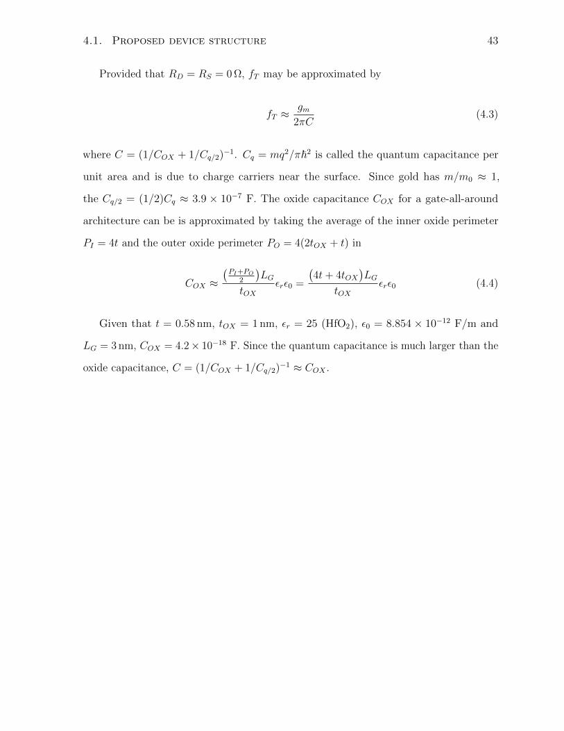
Provided that RD = RS = 0 Ω, fT may be approximated by
fT ≈gm
2πC(4.3)
where C = (1/COX + 1/Cq/2)−1. Cq = mq2/π~2 is called the quantum capacitance per
unit area and is due to charge carriers near the surface. Since gold has m/m0 ≈ 1,
the Cq/2 = (1/2)Cq ≈ 3.9 × 10⁻⁷ F. The oxide capacitance COX for a gate-all-around
architecture can be is approximated by taking the average of the inner oxide perimeter
PI = 4t and the outer oxide perimeter PO = 4(2tOX + t) in
COX ≈(PI+PO
2
)LG
tOXεrε0 =
(4t+ 4tOX
)LG
tOXεrε0 (4.4)
Given that t = 0.58 nm, tOX = 1 nm, εr = 25 (HfO2), ε0 = 8.854 × 10⁻¹² F/m and
LG = 3 nm, COX = 4.2× 10⁻¹⁸ F. Since the quantum capacitance is much larger than the
oxide capacitance, C = (1/COX + 1/Cq/2)−1 ≈ COX .
Chapter 5
Performance simulation
The device outlined in the previous chapter has been systematically simulated by varying
one parameter at a time in order to be able to make firm comparisons.
5.1 Ungated gold channel
The FET channel was first simulated without a gate or oxide to determine its I-V
characteristics. Figure 5.1 shows what channels looks like at lengths of 3-5 nm. Figure 5.2
displays the I-V relation for various lengths. The curves show that the current is
independent of length.
If the simple assumption is made that even at these dimensions, Ohm’s law applies, it
is expected that the current is:
IDS =VDSR
=tW
ρLVDS (5.1)
Given that t = 0.58 nm, W = 0.87 nm, ρ = 2.44× 10⁻⁸ Ωm (resistivity of bulk gold), and
L = 3 nm, and VDS = 0.4V , an IDS = 2.75 mA is predicted.
The self-consistent simulated current at these dimensions results in a current of 110µA.
The simulated current is 25 times smaller than the predicted from Ohm’s Law based on
44
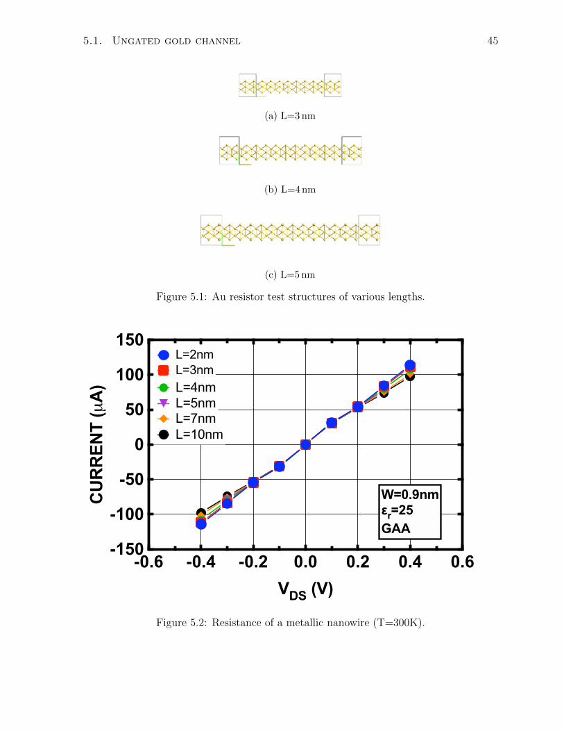
5.1. Ungated gold channel 45
(a) L=3 nm
(b) L=4 nm
(c) L=5 nm
Figure 5.1: Au resistor test structures of various lengths.
-0.6 -0.4 -0.2 0.0 0.2 0.4 0.6-150
-100
-50
0
50
100
150
VDS (V)
CU
RR
EN
T (µ
A)
L=2nm
L=3nm
W=0.9nmεr=25
GAA
L=4nm
L=5nm
L=7nm
L=10nm
Figure 5.2: Resistance of a metallic nanowire (T=300K).
46 Chapter 5. Performance simulation
the resistivity of bulk gold. This is attributed to the fact that the number of states in the
channel are significantly reduced compared to bulk.
5.2 Modulation of DOS
For the purpose of representing the modulation of electrons in the channel, three bias
points were selected VGS = −2.5, 0, 1V . These bias points correspond to the OFF-state,
zero-bias, and maximum current, respectively. In Figure 5.3, the external electrostatic
potential V ext due to the gate voltage VGS is shown along the channel length. The poten-
tial is positive for negative voltages. Along the gate region, the electrostatic potential
is strongest and falls off to 0 eV toward the electrodes. To represent these conditions,
Poisson’s equation is solved by using Neumann boundary conditions in the Y and Z
directions, and Dirichlet boundary condition in the X direction. The Electron Difference
Density, as calculated in Eqn. 3.5 is plotted in Figure 5.4. It is defined as the difference
between the self-consistent valence charge density and the superposition of atomic valence
densities. The atomic valence density is the density of electrons in the valence band
(free electrons) under zero bias (VDS = 0V , VGS = 0V ), while the self-consistent valence
charge density is the one calculated at VGS = −2.5V and VGS = 1V. A negative electron
difference density implies that the atomic valence density is larger than the calculated
charge density. This quantity is appropriate due to the fact that a metallic channel should
have a relatively high concentration of free carriers. Note the conversion, A−3 = 1024cm−3.
It is observed that at VGS = −2.5V , the electron density in the channel is much
lower than the atomic valence density. In fact, the density is 7.8× 1021cm−3 lower. This
demonstrates partial depletion of the channel due to a lack of states in the channel. At
VGS = 0V , the difference between densities is 0cm−3 hence there are free carriers as usual
for metal. At VGS = 1V , it is observed that an enhancement in the density of carriers is
5.2. Modulation of DOS 47
Figure 5.3: External potential. VDS=0.1V, k=25.
observed, likely due to an increased DOS. Figure 5.5 represents the density of states in the
channel for the applied bias. Conduction of electrons only occurs in the energy interval
between the left and right Fermi levels EF (L) and EF (R). As can be seen from the
48 Chapter 5. Performance simulation
Figure 5.4: Electron Difference density. VDS = 0.1V, εr = 25.
diagram, at VGS = −2.5V a suppression of the DOS causes only a low amount of energy
states to be available in the channel for conduction. There is a fundamental difference
here between a semiconducting channel and a metallic channel. The semiconducting
channel would have no states at all and therefore the current may be completely stopped.
5.3. DC characteristics of the gold FET 49
That is not the case for metals. There will always be some states in the channel. This
is both good and bad. The good part is that when scaled to these dimensions, metals
provide a lot more states than semiconductors and therefore will provide a larger drive
current capability. The bad is that a metallic channel may not be capable to be turned
off completely. This is reflected in the performance of the device as will be seen later.
0.05 0.1000
50
100
150
Energy (eV)
Den
sit
y o
f S
tate
s (
eV
-1)
VGS
=-2.5V
VGS
=1V
VGS
=0V
EF(S) EF(D)VDS
Figure 5.5: Modulation of DOS in metals.
It should be noted in Figure 5.4 that conduction still occurs at the surface of the
metal where the dielectric/metal interface would have greatest effect on the mobility of
the carriers.
5.3 DC characteristics of the gold FET
The simulated transfer characteristics are shown in Figure 5.6. For LG = 3 nm, the
minimum current (IOFF ) detected is 0.33 mA/µm at VGS = −2.5V while the maximum
current (ION) is 10 mA/µm at VGS = 1V . For LG = 5 nm, the minimum current (IOFF )
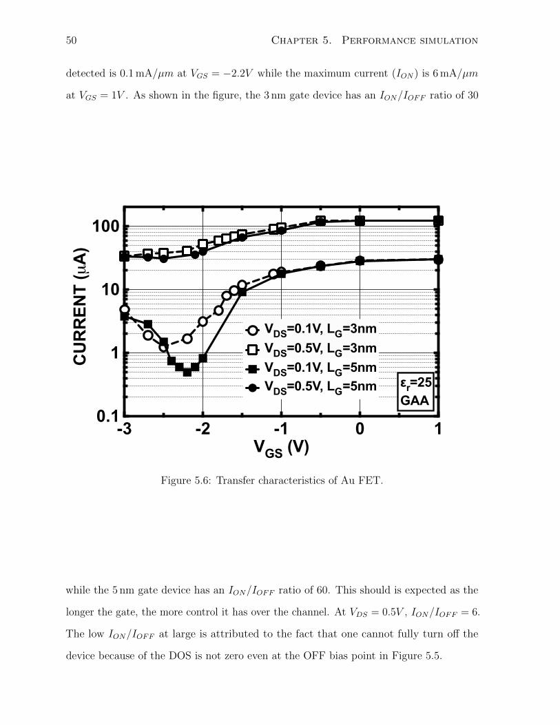
50 Chapter 5. Performance simulation
detected is 0.1 mA/µm at VGS = −2.2V while the maximum current (ION) is 6 mA/µm
at VGS = 1V . As shown in the figure, the 3 nm gate device has an ION/IOFF ratio of 30
-3 -2 -1 0 10.1
1
10
100
VGS (V)
CU
RR
ENT
(µA
)
VDS=0.1V, LG=3nmVDS=0.5V, LG=3nm
εr=25GAA
VDS=0.5V, LG=5nmVDS=0.1V, LG=5nm
Figure 5.6: Transfer characteristics of Au FET.
while the 5 nm gate device has an ION/IOFF ratio of 60. This should is expected as the
longer the gate, the more control it has over the channel. At VDS = 0.5V , ION/IOFF = 6.
The low ION/IOFF at large is attributed to the fact that one cannot fully turn off the
device because of the DOS is not zero even at the OFF bias point in Figure 5.5.
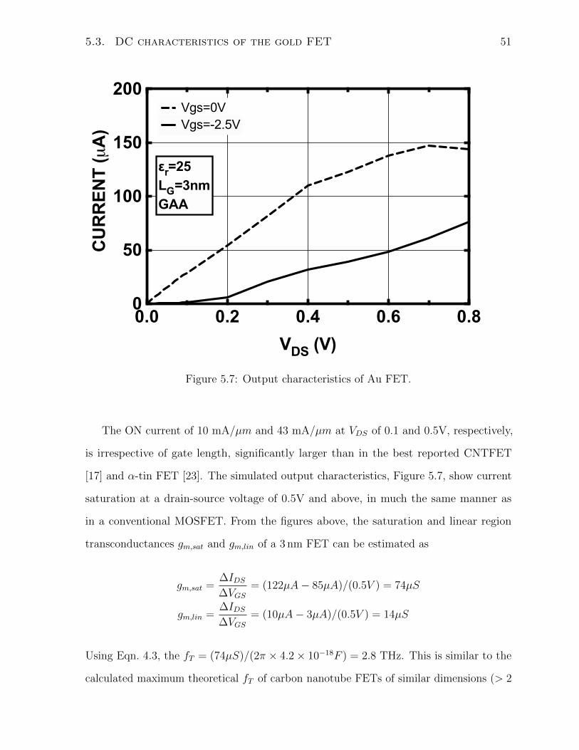
5.3. DC characteristics of the gold FET 51
0.0 0.2 0.4 0.6 0.80
50
100
150
200
VDS (V)
CU
RR
EN
T (µ
A)
Vgs=0V
Vgs=-2.5V
εr=25
LG=3nm
GAA
Figure 5.7: Output characteristics of Au FET.
The ON current of 10 mA/µm and 43 mA/µm at VDS of 0.1 and 0.5V, respectively,
is irrespective of gate length, significantly larger than in the best reported CNTFET
[17] and α-tin FET [23]. The simulated output characteristics, Figure 5.7, show current
saturation at a drain-source voltage of 0.5V and above, in much the same manner as
in a conventional MOSFET. From the figures above, the saturation and linear region
transconductances gm,sat and gm,lin of a 3 nm FET can be estimated as
gm,sat =∆IDS∆VGS
= (122µA− 85µA)/(0.5V ) = 74µS
gm,lin =∆IDS∆VGS
= (10µA− 3µA)/(0.5V ) = 14µS
Using Eqn. 4.3, the fT = (74µS)/(2π × 4.2× 10−18F ) = 2.8 THz. This is similar to the
calculated maximum theoretical fT of carbon nanotube FETs of similar dimensions (> 2
52 Chapter 5. Performance simulation
THz) [41]. The complete python code for the 3 nm gold FET simulation is included in
Appendix A.
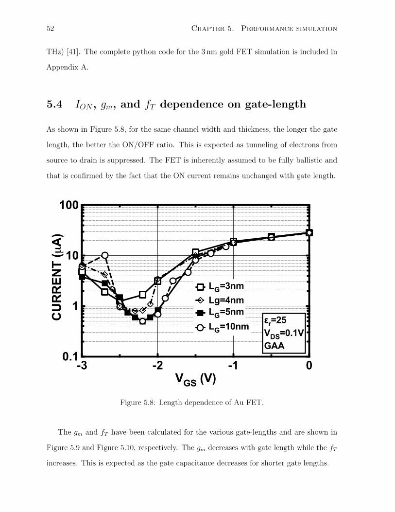
5.4 ION , gm, and fT dependence on gate-length
As shown in Figure 5.8, for the same channel width and thickness, the longer the gate
length, the better the ON/OFF ratio. This is expected as tunneling of electrons from
source to drain is suppressed. The FET is inherently assumed to be fully ballistic and
that is confirmed by the fact that the ON current remains unchanged with gate length.
-3 -2 -1 00.1
1
10
100
VGS (V)
CU
RR
EN
T (µ
A)
LG=5nm
LG=10nmεr=25
VDS=0.1V
GAA
LG=3nm
Lg=4nm
Figure 5.8: Length dependence of Au FET.
The gm and fT have been calculated for the various gate-lengths and are shown in
Figure 5.9 and Figure 5.10, respectively. The gm decreases with gate length while the fT
increases. This is expected as the gate capacitance decreases for shorter gate lengths.
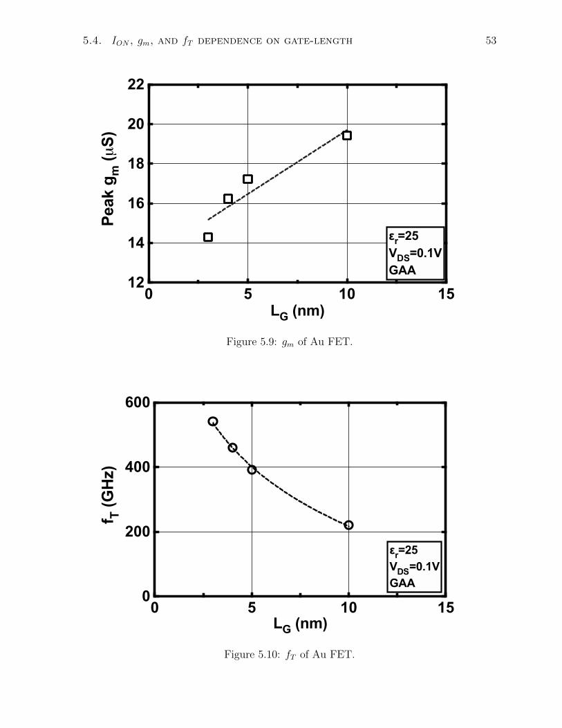
5.4. ION , gm, and fT dependence on gate-length 53
0 5 10 1512
14
16
18
20
22
LG (nm)
Peak g
m (µ
S)
εr=25
VDS=0.1V
GAA
Figure 5.9: gm of Au FET.
0 5 10 150
200
400
600
LG (nm)
f T (
GH
z)
εr=25
VDS
=0.1V
GAA
Figure 5.10: fT of Au FET.
54 Chapter 5. Performance simulation
5.5 Channel width dependence
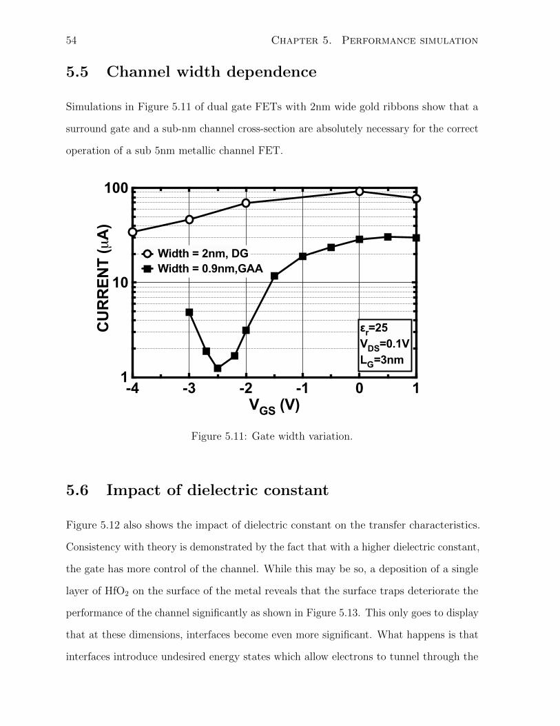
Simulations in Figure 5.11 of dual gate FETs with 2nm wide gold ribbons show that a
surround gate and a sub-nm channel cross-section are absolutely necessary for the correct
operation of a sub 5nm metallic channel FET.
-4 -3 -2 -1 0 11
10
100
VGS (V)
CU
RR
EN
T (µ
A)
Width = 2nm, DG
εr=25
VDS=0.1V
LG=3nm
Width = 0.9nm,GAA
Figure 5.11: Gate width variation.
5.6 Impact of dielectric constant
Figure 5.12 also shows the impact of dielectric constant on the transfer characteristics.
Consistency with theory is demonstrated by the fact that with a higher dielectric constant,
the gate has more control of the channel. While this may be so, a deposition of a single
layer of HfO2 on the surface of the metal reveals that the surface traps deteriorate the
performance of the channel significantly as shown in Figure 5.13. This only goes to display
that at these dimensions, interfaces become even more significant. What happens is that
interfaces introduce undesired energy states which allow electrons to tunnel through the
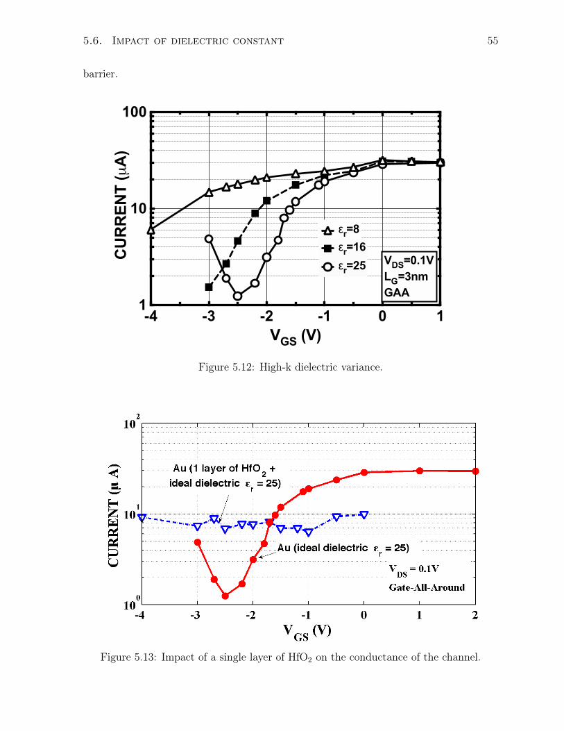
5.6. Impact of dielectric constant 55
barrier.
-4 -3 -2 -1 0 11
10
100
VGS (V)
CU
RR
EN
T (µ
A)
εr=8
εr=25
εr=16VDS=0.1V
LG=3nm
GAA
Figure 5.12: High-k dielectric variance.
Figure 5.13: Impact of a single layer of HfO2 on the conductance of the channel.
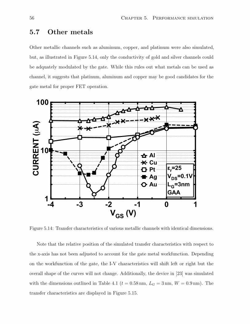
56 Chapter 5. Performance simulation
5.7 Other metals
Other metallic channels such as aluminum, copper, and platinum were also simulated,
but, as illustrated in Figure 5.14, only the conductivity of gold and silver channels could
be adquately modulated by the gate. While this rules out what metals can be used as
channel, it suggests that platinum, aluminum and copper may be good candidates for the
gate metal for proper FET operation.
-4 -3 -2 -1 0 11
10
100
VGS (V)
CU
RR
EN
T (µ
A)
Au
Pt
Cu
Ag
εr=25
VDS=0.1V
LG=3nm
GAA
Al
Figure 5.14: Transfer characteristics of various metallic channels with identical dimensions.
Note that the relative position of the simulated transfer characteristics with respect to
the x-axis has not been adjusted to account for the gate metal workfunction. Depending
on the workfunction of the gate, the I-V characteristics will shift left or right but the
overall shape of the curves will not change. Additionally, the device in [23] was simulated
with the dimensions outlined in Table 4.1 (t = 0.58 nm, LG = 3 nm, W = 0.9 nm). The
transfer characteristics are displayed in Figure 5.15.
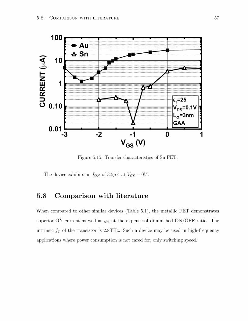
5.8. Comparison with literature 57
-3 -2 -1 0 10.01
0.10
1
10
100
VGS (V)
CU
RR
EN
T (µ
A)
εr=25
VDS
=0.1V
LG
=3nm
GAA
Au
Sn
Figure 5.15: Transfer characteristics of Sn FET.
The device exhibits an ION of 3.5µA at VGS = 0V .
5.8 Comparison with literature
When compared to other similar devices (Table 5.1), the metallic FET demonstrates
superior ON current as well as gm at the expense of diminished ON/OFF ratio. The
intrinsic fT of the transistor is 2.8THz. Such a device may be used in high-frequency
applications where power consumption is not cared for, only switching speed.
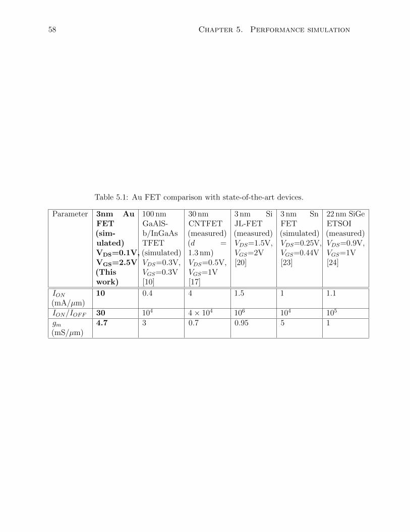
58 Chapter 5. Performance simulation
Table 5.1: Au FET comparison with state-of-the-art devices.
Parameter 3nm AuFET(sim-ulated)VDS=0.1V,VGS=2.5V(Thiswork)
100 nmGaAlS-b/InGaAsTFET(simulated)VDS=0.3V,VGS=0.3V[10]
30 nmCNTFET(measured)(d =1.3 nm)VDS=0.5V,VGS=1V[17]
3 nm SiJL-FET(measured)VDS=1.5V,VGS=2V[20]
3 nm SnFET(simulated)VDS=0.25V,VGS=0.44V[23]
22 nm SiGeETSOI(measured)VDS=0.9V,VGS=1V[24]
ION(mA/µm)
10 0.4 4 1.5 1 1.1
ION/IOFF 30 104 4× 10⁴ 106 104 105
gm(mS/µm)
4.7 3 0.7 0.95 5 1
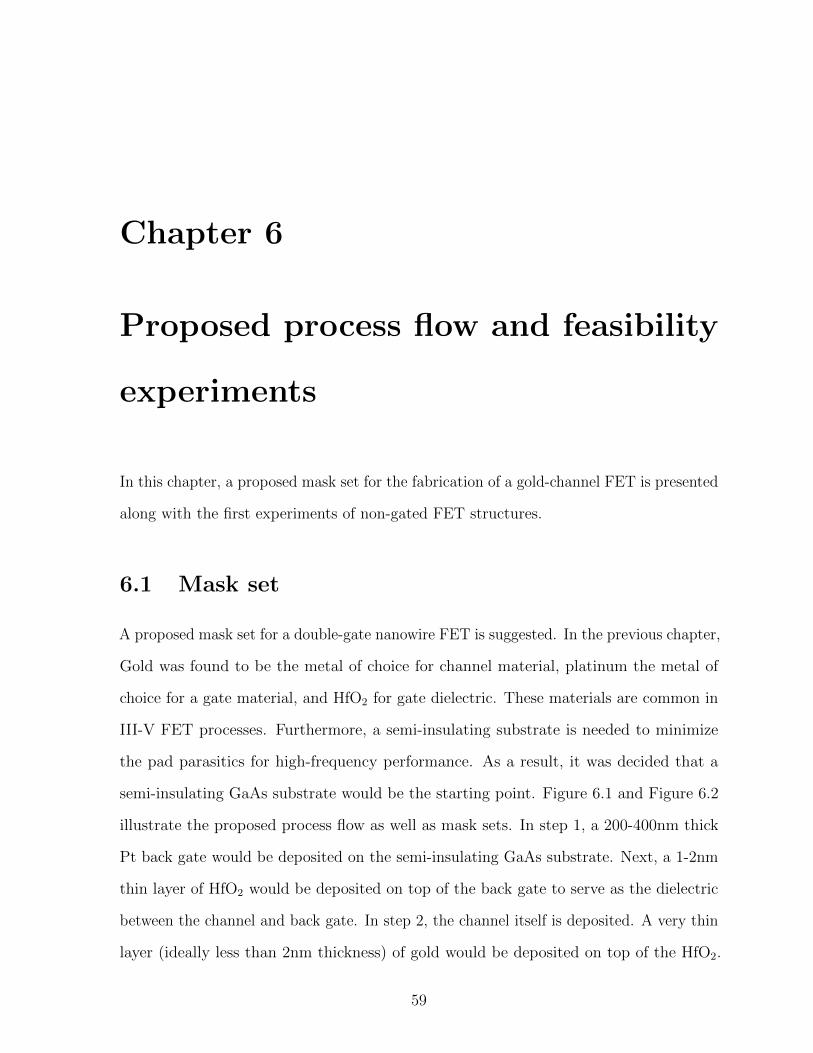
Chapter 6
Proposed process flow and feasibility
experiments
In this chapter, a proposed mask set for the fabrication of a gold-channel FET is presented
along with the first experiments of non-gated FET structures.
6.1 Mask set
A proposed mask set for a double-gate nanowire FET is suggested. In the previous chapter,
Gold was found to be the metal of choice for channel material, platinum the metal of
choice for a gate material, and HfO2 for gate dielectric. These materials are common in
III-V FET processes. Furthermore, a semi-insulating substrate is needed to minimize
the pad parasitics for high-frequency performance. As a result, it was decided that a
semi-insulating GaAs substrate would be the starting point. Figure 6.1 and Figure 6.2
illustrate the proposed process flow as well as mask sets. In step 1, a 200-400nm thick
Pt back gate would be deposited on the semi-insulating GaAs substrate. Next, a 1-2nm
thin layer of HfO2 would be deposited on top of the back gate to serve as the dielectric
between the channel and back gate. In step 2, the channel itself is deposited. A very thin
layer (ideally less than 2nm thickness) of gold would be deposited on top of the HfO2.
59
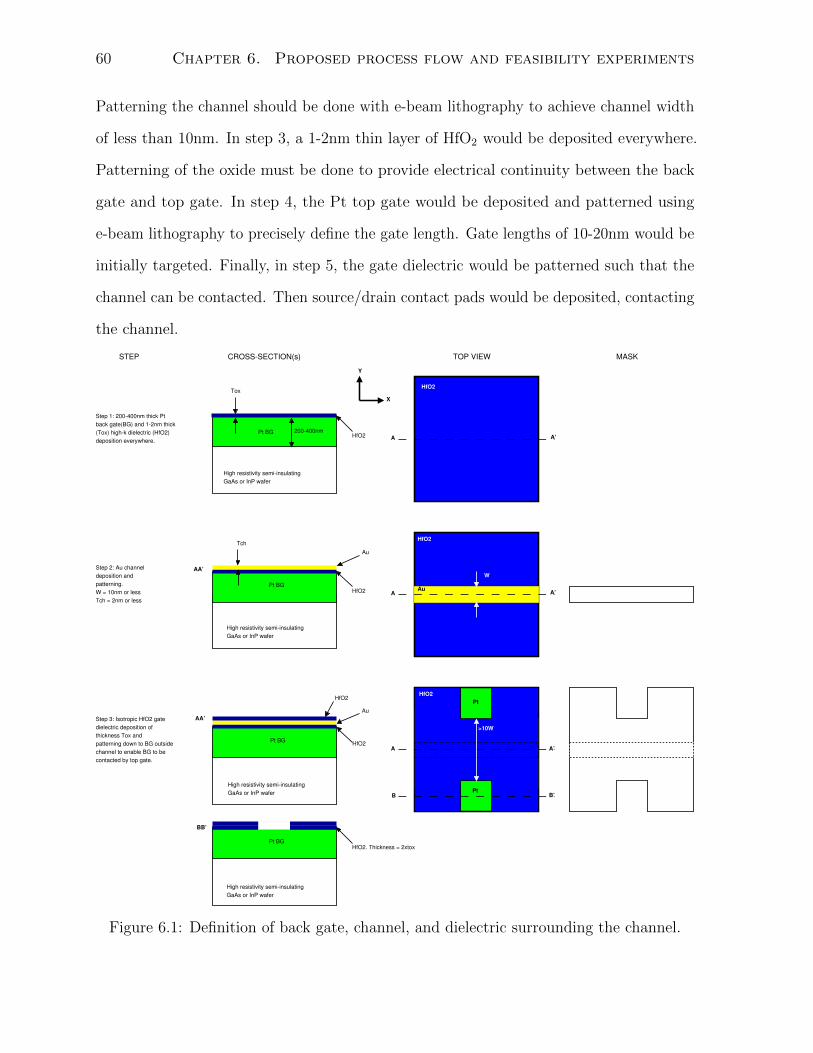
60 Chapter 6. Proposed process flow and feasibility experiments
Patterning the channel should be done with e-beam lithography to achieve channel width
of less than 10nm. In step 3, a 1-2nm thin layer of HfO2 would be deposited everywhere.
Patterning of the oxide must be done to provide electrical continuity between the back
gate and top gate. In step 4, the Pt top gate would be deposited and patterned using
e-beam lithography to precisely define the gate length. Gate lengths of 10-20nm would be
initially targeted. Finally, in step 5, the gate dielectric would be patterned such that the
channel can be contacted. Then source/drain contact pads would be deposited, contacting
the channel.
High resistivity semi-insulating
GaAs or InP wafer
Step 1: 200-400nm thick Pt
back gate(BG) and 1-2nm thick
(Tox) high-k dielectric (HfO2)
deposition everywhere.
CROSS-SECTION(s) TOP VIEW
A
High resistivity semi-insulating
GaAs or InP wafer
Step 2: Au channel
deposition and
patterning.
W = 10nm or less
Tch = 2nm or less
A’
X
Y
A A’
Pt BG
Pt BG
MASK
High resistivity semi-insulating
GaAs or InP wafer
Step 3: Isotropic HfO2 gate
dielectric deposition of
thickness Tox and
patterning down to BG outside
channel to enable BG to be
contacted by top gate.
A A’
Pt BG
HfO2
HfO2
Au
Au
HfO2
HfO2
HfO2
Pt
HfO2
Au
W
Pt
HfO2
>10W
B B’
High resistivity semi-insulating
GaAs or InP wafer
Pt BGHfO2. Thickness = 2xtox
BB’
Tox
200-400nm
AA’
AA’
STEP
Tch
Figure 6.1: Definition of back gate, channel, and dielectric surrounding the channel.
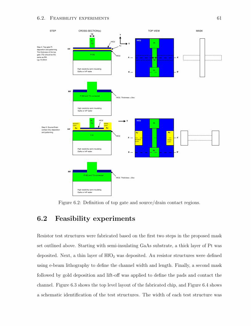
6.2. Feasibility experiments 61
CROSS-SECTION(s) TOP VIEW MASKSTEP
High resistivity semi-insulating
GaAs or InP wafer
Step 4: Top gate Pt
deposition and patterning.
The thickness of the top
gate (TG) should be the
same as BG.
Lg=10-20nm
A A’
Pt BG
HfO2
Pt
HfO2
Au
Pt
HfO2
B B’
AA’
High resistivity semi-insulating
GaAs or InP wafer
HfO2. Thickness = 2tox
BB’
Pt
TG
Pt BG and TG connected
Lg
Lg
XHfO2
High resistivity semi-insulating
GaAs or InP wafer
Step 5: Source/Drain
contact (Au) deposition
and patterning.
A A’
Pt BG
HfO2
Pt
HfO2
PtB B’
AA’
High resistivity semi-insulating
GaAs or InP wafer
HfO2. Thickness = 2tox
BB’
Pt
TG
Pt BG and TG connected
SOURCE
CONT.
DRAIN
CONT.
HfO2
SOURCE
CONT.DRAIN
CONT.
Au Au
Au Au
X
Y
Figure 6.2: Definition of top gate and source/drain contact regions.
6.2 Feasibility experiments
Resistor test structures were fabricated based on the first two steps in the proposed mask
set outlined above. Starting with semi-insulating GaAs substrate, a thick layer of Pt was
deposited. Next, a thin layer of HfO2 was deposited. Au resistor structures were defined
using e-beam lithography to define the channel width and length. Finally, a second mask
followed by gold deposition and lift-off was applied to define the pads and contact the
channel. Figure 6.3 shows the top level layout of the fabricated chip, and Figure 6.4 shows
a schematic identification of the test structures. The width of each test structure was
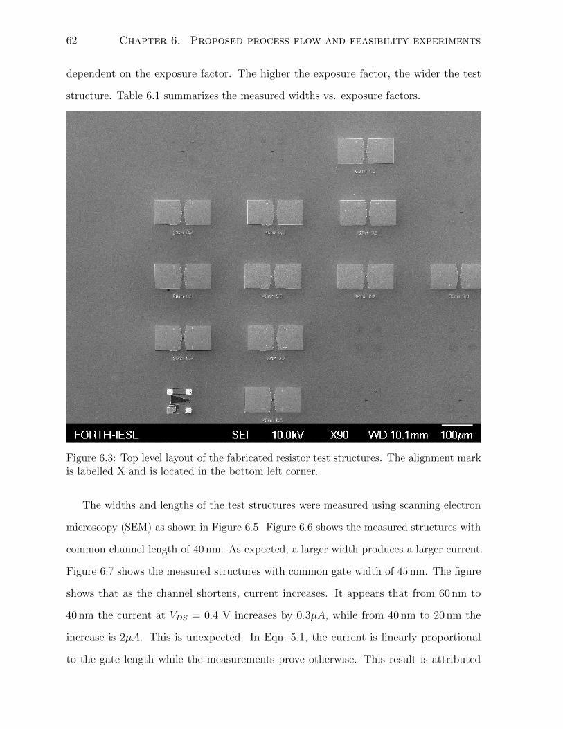
62 Chapter 6. Proposed process flow and feasibility experiments
dependent on the exposure factor. The higher the exposure factor, the wider the test
structure. Table 6.1 summarizes the measured widths vs. exposure factors.
Figure 6.3: Top level layout of the fabricated resistor test structures. The alignment markis labelled X and is located in the bottom left corner.
The widths and lengths of the test structures were measured using scanning electron
microscopy (SEM) as shown in Figure 6.5. Figure 6.6 shows the measured structures with
common channel length of 40 nm. As expected, a larger width produces a larger current.
Figure 6.7 shows the measured structures with common gate width of 45 nm. The figure
shows that as the channel shortens, current increases. It appears that from 60 nm to
40 nm the current at VDS = 0.4 V increases by 0.3µA, while from 40 nm to 20 nm the
increase is 2µA. This is unexpected. In Eqn. 5.1, the current is linearly proportional
to the gate length while the measurements prove otherwise. This result is attributed
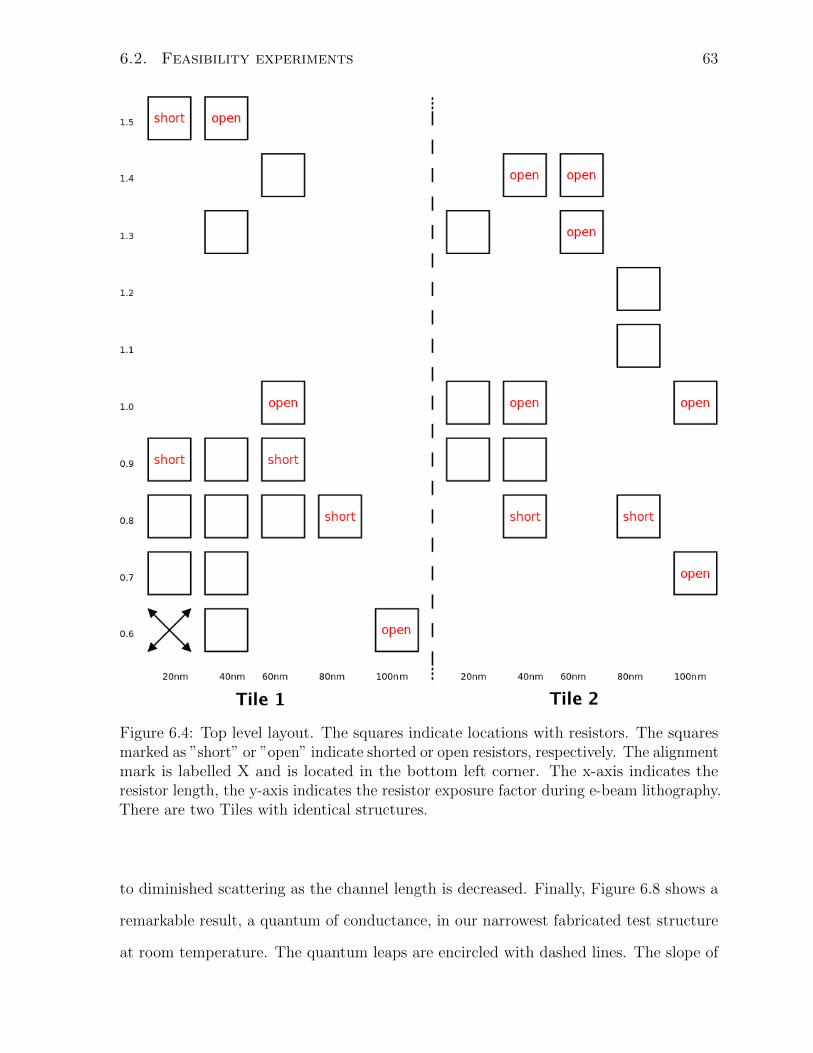
6.2. Feasibility experiments 63
Figure 6.4: Top level layout. The squares indicate locations with resistors. The squaresmarked as ”short” or ”open” indicate shorted or open resistors, respectively. The alignmentmark is labelled X and is located in the bottom left corner. The x-axis indicates theresistor length, the y-axis indicates the resistor exposure factor during e-beam lithography.There are two Tiles with identical structures.
to diminished scattering as the channel length is decreased. Finally, Figure 6.8 shows a
remarkable result, a quantum of conductance, in our narrowest fabricated test structure
at room temperature. The quantum leaps are encircled with dashed lines. The slope of
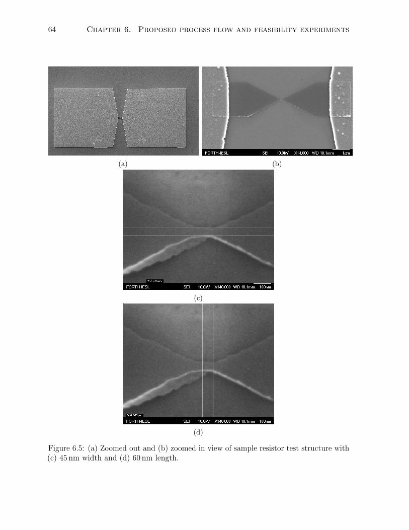
64 Chapter 6. Proposed process flow and feasibility experiments
(a) (b)
(c)
(d)
Figure 6.5: (a) Zoomed out and (b) zoomed in view of sample resistor test structure with(c) 45 nm width and (d) 60 nm length.
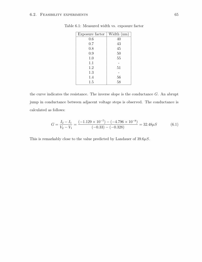
6.2. Feasibility experiments 65
Table 6.1: Measured width vs. exposure factor
Exposure factor Width (nm)0.6 400.7 430.8 450.9 501.0 551.1 -1.2 511.3 -1.4 561.5 58
the curve indicates the resistance. The inverse slope is the conductance G. An abrupt
jump in conductance between adjacent voltage steps is observed. The conductance is
calculated as follows:
G =I2 − I1V2 − V1
=(−1.129× 10⁻⁷)− (−4.796× 10⁻⁸)
(−0.33)− (−0.328)= 32.48µS (6.1)
This is remarkably close to the value predicted by Landauer of 39.6µS.
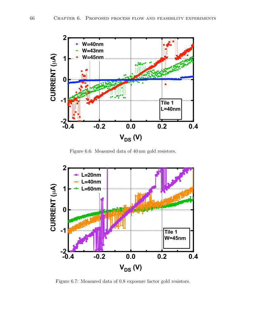
66 Chapter 6. Proposed process flow and feasibility experiments
-0.4 -0.2 0.0 0.2 0.4
0
-2
2
-1
1
VDS (V)
CU
RR
EN
T (µ
A)
Tile 1
L=40nm
W=40nm
W=45nm
W=43nm
Figure 6.6: Measured data of 40 nm gold resistors.
-0.4 -0.2 0.0 0.2 0.4
0
-2
2
-1
1
VDS (V)
CU
RR
EN
T (µ
A)
Tile 1
W=45nm
L=20nm
L=40nm
L=60nm
Figure 6.7: Measured data of 0.8 exposure factor gold resistors.
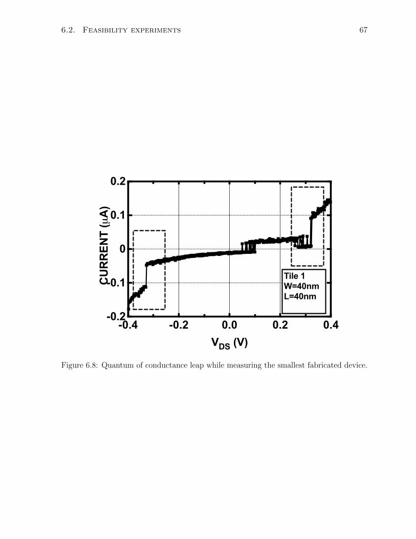
6.2. Feasibility experiments 67
-0.4 -0.2 0.0 0.2 0.4
0
-0.1
0.1
-0.2
0.2
VDS (V)
CU
RR
EN
T (µ
A)
Tile 1
W=40nm
L=40nm
Figure 6.8: Quantum of conductance leap while measuring the smallest fabricated device.
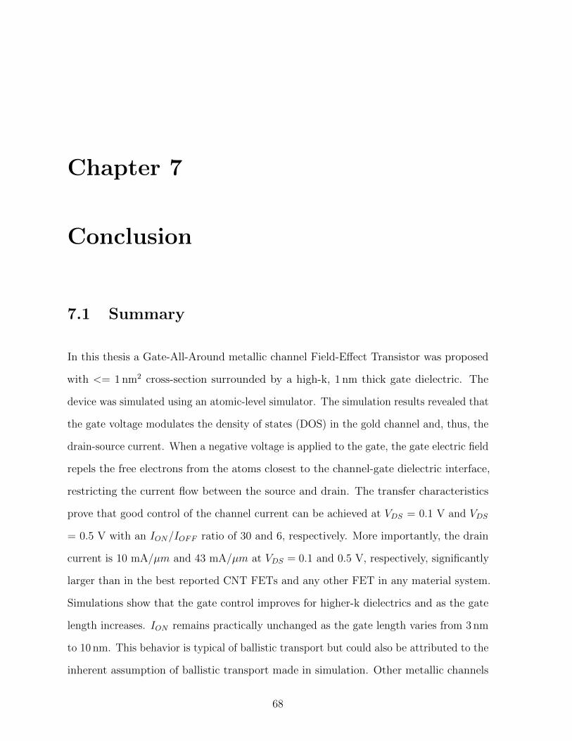
Chapter 7
Conclusion
7.1 Summary
In this thesis a Gate-All-Around metallic channel Field-Effect Transistor was proposed
with <= 1 nm2 cross-section surrounded by a high-k, 1 nm thick gate dielectric. The
device was simulated using an atomic-level simulator. The simulation results revealed that
the gate voltage modulates the density of states (DOS) in the gold channel and, thus, the
drain-source current. When a negative voltage is applied to the gate, the gate electric field
repels the free electrons from the atoms closest to the channel-gate dielectric interface,
restricting the current flow between the source and drain. The transfer characteristics
prove that good control of the channel current can be achieved at VDS = 0.1 V and VDS
= 0.5 V with an ION/IOFF ratio of 30 and 6, respectively. More importantly, the drain
current is 10 mA/µm and 43 mA/µm at VDS = 0.1 and 0.5 V, respectively, significantly
larger than in the best reported CNT FETs and any other FET in any material system.
Simulations show that the gate control improves for higher-k dielectrics and as the gate
length increases. ION remains practically unchanged as the gate length varies from 3 nm
to 10 nm. This behavior is typical of ballistic transport but could also be attributed to the
inherent assumption of ballistic transport made in simulation. Other metallic channels
68
7.2. Future Work 69
such as aluminum, copper, and platinum were also simulated, but only the conductivity
of gold and silver channels could be modulated by the gate. This suggests that platinum,
aluminum and copper may be good candidates for the gate metal. Simulations also show
that a surround gate and a sub-nm channel cross-section are absolutely necessary for
the correct operation of a sub 5nm metallic channel FET. The intrinsic fT of 3 nm gate
length device is approximated to be 2.8THz which is comparable to theoretical limit of
carbon nanotube FETs of similar dimensions. A mask set for the fabrication of the device
was developed in Chapter 6. It is considerably simpler than that of a MOSFET. Initial
feasibility experiments were conducted on ungated gold channels. A conductance jump
resembling the Landauer quantum of conductance was observed.
7.2 Future Work
The focus on this thesis was to prove in simulation the feasibility of the metallic channel
FET. An obvious extension of this work is the complete fabrication of the proposed
structure based on the proposed mask set. The FET may be improved, by using a
cylindrical surround gate rather than rectangular. The crystal orientation can be varied
to optimize ION . Different gate dielectrics can be tried to produce a defect-free interface
with the channel. Other metals should also be investigated for channel materials.
Bibliography
[1] I. Ferain, C. A. Colinge, and J.-P. Colinge, “Multigate transistors as the future of
classical metaloxidesemiconductor field-effect transistors,” Nature, vol. 479, pp. 310–
316, Nov. 2011.
[2] S. Voinigescu, High-frequency integrated circuits. Cambridge: Cambridge University
Press, 2013.
[3] Y. Taur and T. H. Ning, Fundamentals of Modern VLSI Devices. Cambridge
University Press, 1 ed., Oct. 1998.
[4] K.-M. Liu, L. F. Register, and S. K. Banerjee, “Quantum transport simulation of
strain and orientation effects in sub-20 nm silicon-on-insulator FinFETs,” IEEE
Transactions on Electron Devices, vol. 58, pp. 4–10, Jan. 2011.
[5] G. Groeseneken, L. Pantisano, L.-A. Ragnarsson, R. Degraeve, M. Houssa, T. Kauer-
auf, P. Roussel, S. De Gendt, and M. Heyns, “Achievements and challenges for the
electrical performance of MOSFETs with high-k gate dielectrics,” in Physical and
Failure Analysis of Integrated Circuits, 2004. IPFA 2004. Proceedings of the 11th
International Symposium on the, p. 147155, 2004.
[6] K. J. Kuhn, “CMOS scaling for the 22nm node and beyond: Device physics and
technology,” in VLSI Technology, Systems and Applications (VLSI-TSA), 2011
International Symposium on, p. 12, 2011.
70
Bibliography 71
[7] W. Chern, P. Hashemi, J. T. Teherani, T. Yu, Y. Dong, G. Xia, D. A. Antoniadis,
and J. L. Hoyt, “High mobility high--all-around asymmetrically-strained germanium
nanowire trigate p-MOSFETs,” in Electron Devices Meeting (IEDM), 2012 IEEE
International, p. 165, 2012.
[8] A. M. Ionescu and H. Riel, “Tunnel field-effect transistors as energy-efficient electronic
switches,” Nature, vol. 479, pp. 329–337, Nov. 2011.
[9] P. Asbeck, L. Wang, S. Gu, Y. Taur, and E. Yu, “Tunneling MOSFETs based
on III-V staggered heterojunctions,” MRS Online Proceedings Library, vol. 1252,
pp. null–null, 2010.
[10] L. Wang, E. Yu, Y. Taur, and P. Asbeck, “Design of tunneling field-effect transistors
based on staggered heterojunctions for ultralow-power applications,” IEEE Electron
Device Letters, vol. 31, pp. 431 –433, May 2010.
[11] J. Moon, D. Curtis, M. Hu, S. Bui, D. Wheeler, T. Marshall, H. Sharifi, D. Wong,
D. Gaskill, P. Campbell, P. Asbeck, G. Jernigan, J. Tedesco, B. VanMil, R. Myers-
Ward, C. Eddy, X. Weng, J. Robinson, and M. Fanton, “Self-aligned graphene-on-SiC
and graphene-on-si MOSFETs on 75 mm wafers,” in Device Research Conference
(DRC), 2010, pp. 209 –210, June 2010.
[12] V. Barone, O. Hod, and G. E. Scuseria, “Electronic structure and stability of
semiconducting graphene nanoribbons,” Nano Letters, vol. 6, pp. 2748–2754, Dec.
2006.
[13] M. Y. Han, B. Oezyilmaz, Y. Zhang, and P. Kim, “Energy band gap engineering of
graphene nanoribbons,” arXiv:cond-mat/0702511, Feb. 2007. Phys. Rev. Lett, 98,
206805 (2007).
[14] J. Moon, M. Antcliffe, H. Seo, S. Lin, A. Schmitz, I. Milosavljevic, K. McCalla,
D. Wong, D. Gaskill, P. Campbell, K.-M. Lee, and P. Asbeck, “Graphene review: An
72 Bibliography
emerging RF technology,” in 2012 IEEE 12th Topical Meeting on Silicon Monolithic
Integrated Circuits in RF Systems (SiRF), pp. 199 –202, Jan. 2012.
[15] B. Radisavljevic, A. Radenovic, J. Brivio, V. Giacometti, and A. Kis, “Single-layer
MoS2 transistors,” Nature Nanotechnology, vol. 6, no. 3, pp. 147–150, 2011.
[16] H. Wang, T. Taychatanapat, A. Hsu, K. Watanabe, T. Taniguchi, P. Jarillo-Herrero,
and T. Palacios, “BN/Graphene/BN transistors for RF applications,” IEEE Electron
Device Letters, vol. 32, pp. 1209–1211, Sept. 2011.
[17] A. D. Franklin, S. O. Koswatta, D. Farmer, G. S. Tulevski, J. T. Smith, H. Miyazoe,
and W. Haensch, “Scalable and fully self-aligned n-type carbon nanotube transistors
with gate-all-around,” in Electron Devices Meeting (IEDM), 2012 IEEE International,
p. 45, 2012.
[18] L. J. Edgar, “Method and apparatus for controlling electric currents,” Jan. 1930.
U.S. Classification 330/309, 257/E29.296, 257/43, 257/73, 327/581, 330/277, 257/66;
International Classification H03F3/04, H01L29/786, H01L29/00; Cooperative Classi-
fication H01L29/78681, H01L29/00, H03F3/04; European Classification H01L29/00,
H01L29/786F, H03F3/04.
[19] S. V. Rotkin and K. Hess, “Principles of metallic field effect transistor (METFET),”
in Technical Proceedings of the 2003 Nanotechnology Conference and Trade Show,
vol. 1, p. 3, 2004.
[20] S. Migita, Y. Morita, M. Masahara, and H. Ota, “Electrical performances of
junctionless-FETs at the scaling limit (l CH= 3 nm),” in Electron Devices Meeting
(IEDM), 2012 IEEE International, p. 86, 2012.
[21] J.-P. Colinge, C.-W. Lee, A. Afzalian, N. D. Akhavan, R. Yan, I. Ferain, P. Razavi,
B. O’Neill, A. Blake, M. White, A.-M. Kelleher, B. McCarthy, and R. Murphy,
Bibliography 73
“Nanowire transistors without junctions,” Nature Nanotechnology, vol. 5, no. 3,
pp. 225–229, 2010.
[22] H. Cheng, C. Andrew, and M. Alkaisi, “The fabrication and characterisation of
metallic nanotransistors,” Microelectronic Engineering, vol. 83, pp. 1749–1752, Apr.
2006.
[23] L. Ansari, G. Fagas, J.-P. Colinge, and J. C. Greer, “A proposed confinement
modulated gap nanowire transistor based on a metal (tin),” Nano Letters, vol. 12,
pp. 2222–2227, May 2012.
[24] K. Cheng, A. Khakifirooz, N. Loubet, S. Luning, T. Nagumo, M. Vinet, Q. Liu,
A. Reznicek, T. Adam, and S. Naczas, “High performance extremely thin SOI
(ETSOI) hybrid CMOS with si channel NFET and strained SiGe channel PFET,” in
Electron Devices Meeting (IEDM), 2012 IEEE International, p. 181, 2012.
[25] N. W. Ashcroft and N. D. Mermin, Solid state physics. New York; London: Harcourt
College Publishers, 1976.
[26] J. P. McKelvey, Solid State and Semiconductor Physics. Krieger Publishing Company,
1966.
[27] A. Majumdar, Z. Ren, S. J. Koester, and W. Haensch, “Undoped-body extremely thin
SOI MOSFETs with back gates,” IEEE Transactions on Electron Devices, vol. 56,
pp. 2270–2276, Oct. 2009.
[28] D.-H. Kim and J. del Alamo, “Lateral and vertical scaling of $\hboxIn 0.7
\hboxGa 0.3\hboxAs$ HEMTs for post-si-CMOS logic applications,” IEEE
Transactions on Electron Devices, vol. 55, pp. 2546–2553, Oct. 2008.
[29] Y. Liu, H. S. Pal, M. S. Lundstrom, D.-H. Kim, J. A. d. Alamo, and D. A. Anto-
niadis, “Device physics and performance potential of III-V field-effect transistors,”
74 Bibliography
in Fundamentals of III-V Semiconductor MOSFETs (S. Oktyabrsky and P. Ye, eds.),
pp. 31–50, Boston, MA: Springer US, 2010.
[30] C. Jeong, D. A. Antoniadis, and M. S. Lundstrom, “On backscattering and mobility
in nanoscale silicon MOSFETs,” IEEE Transactions on Electron Devices, vol. 56,
pp. 2762–2769, Nov. 2009.
[31] W. R. Frensley, “VLSI electronics: Microstructure science.(academic press, san diego)
publication date: March 25, 1994,” 1998.
[32] S. Datta, Quantum transport atom to transistor. Cambridge, UK; New York: Cam-
bridge University Press, 2005.
[33] “Manuals | QuantumWise.”
[34] M. Brandbyge, J.-L. Mozos, P. Ordejn, J. Taylor, and K. Stokbro, “Density-functional
method for nonequilibrium electron transport,” Physical Review B, vol. 65, p. 165401,
Mar. 2002.
[35] K. Stokbro, D. E. Petersen, S. Smidstrup, A. Blom, M. Ipsen, and K. Kaasbjerg,
“Semi-empirical model for nano-scale device simulations,” arXiv:1004.2812, Apr. 2010.
[36] J. M. Soler, E. Artacho, J. D. Gale, A. Garca, J. Junquera, P. Ordejn, and D. Snchez-
Portal, “The SIESTA method for ab initio order-n materials simulation,” Journal of
Physics: Condensed Matter, vol. 14, p. 2745, Mar. 2002.
[37] K. A. Johnson and N. W. Ashcroft, “Corrections to density-functional theory band
gaps,” Physical Review B, vol. 58, no. 23, p. 15548, 1998.
[38] D. Segev, A. Janotti, and C. Van de Walle, “Self-consistent band-gap corrections
in density functional theory using modified pseudopotentials,” Physical Review B,
vol. 75, Jan. 2007.
Bibliography 75
[39] I. N. Yakovkin and P. A. Dowben, “The problem of the band gap in LDA calculations,”
Surface Review and Letters, vol. 14, no. 03, p. 481487, 2007.
[40] M. B. Cortie and E. Van der Lingen, “Catalytic gold nanoparticles,” in Materials
Forum, vol. 26, p. 114, 2002.
[41] D. L. Pulfrey, “Critique of high-frequency performance of carbon nanotube FETs,”
in Solid State Device Research Conference, 2007. ESSDERC 2007. 37th European,
p. 234238, 2007.
Appendices
76
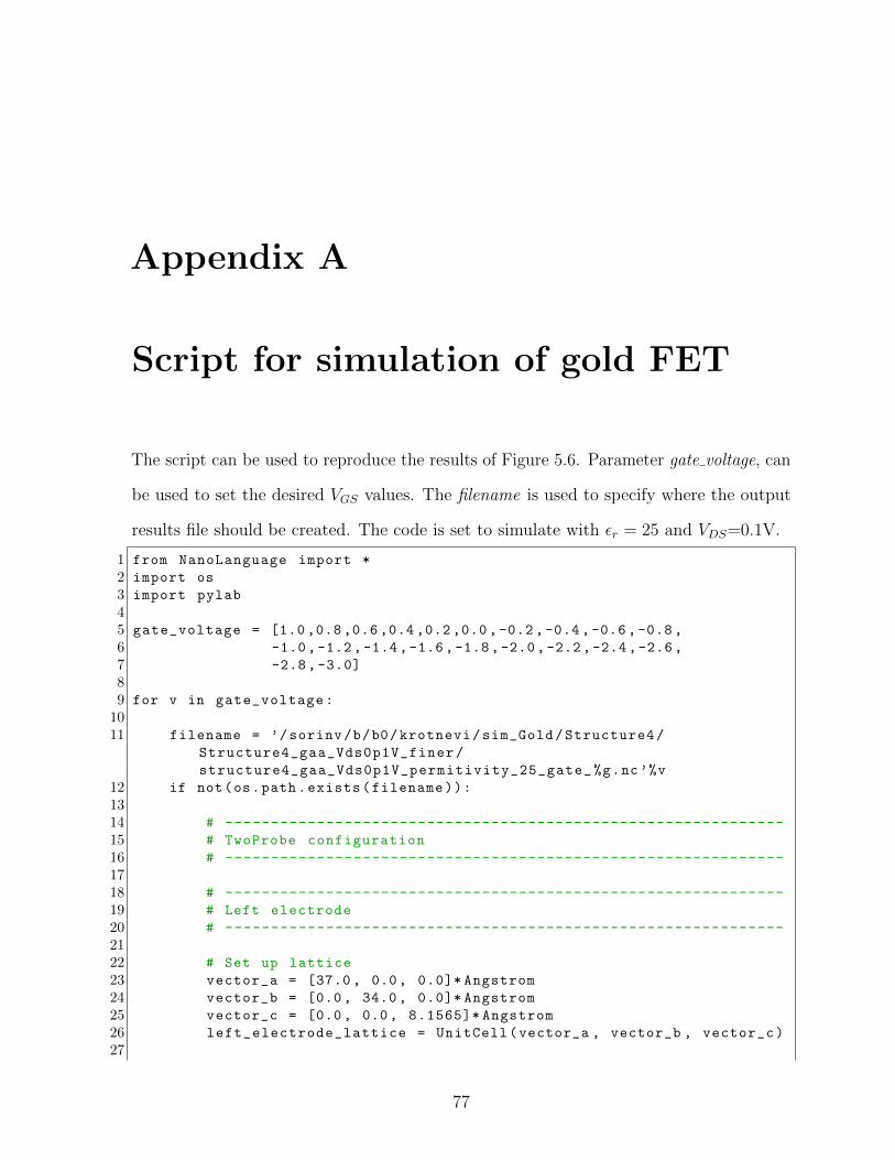
Appendix A
Script for simulation of gold FET
The script can be used to reproduce the results of Figure 5.6. Parameter gate voltage, can
be used to set the desired VGS values. The filename is used to specify where the output
results file should be created. The code is set to simulate with εr = 25 and VDS=0.1V.
1 from NanoLanguage import *
2 import os
3 import pylab
45 gate_voltage = [1.0 ,0.8,0.6,0.4 ,0.2 ,0.0, -0.2 ,-0.4 ,-0.6, -0.8,
6 -1.0,-1.2,-1.4,-1.6,-1.8,-2.0,-2.2,-2.4,-2.6,
7 -2.8,-3.0]
89 for v in gate_voltage:
1011 filename = ’/sorinv/b/b0/krotnevi/sim_Gold/Structure4/
Structure4_gaa_Vds0p1V_finer/
structure4_gaa_Vds0p1V_permitivity_25_gate_%g.nc’%v
12 if not(os.path.exists(filename)):
1314 # -------------------------------------------------------------
15 # TwoProbe configuration
16 # -------------------------------------------------------------
1718 # -------------------------------------------------------------
19 # Left electrode
20 # -------------------------------------------------------------
2122 # Set up lattice
23 vector_a = [37.0 , 0.0, 0.0]* Angstrom
24 vector_b = [0.0, 34.0, 0.0]* Angstrom
25 vector_c = [0.0, 0.0, 8.1565]* Angstrom
26 left_electrode_lattice = UnitCell(vector_a , vector_b , vector_c)
27
77
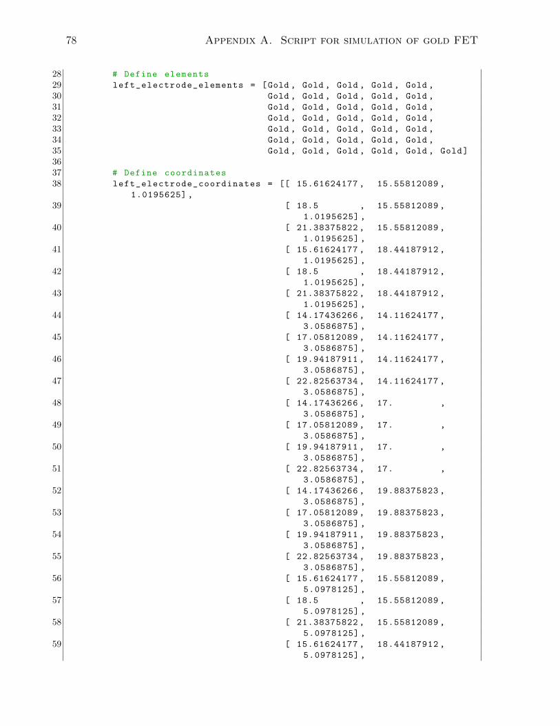
78 Appendix A. Script for simulation of gold FET
28 # Define elements
29 left_electrode_elements = [Gold , Gold , Gold , Gold , Gold ,
30 Gold , Gold , Gold , Gold , Gold ,
31 Gold , Gold , Gold , Gold , Gold ,
32 Gold , Gold , Gold , Gold , Gold ,
33 Gold , Gold , Gold , Gold , Gold ,
34 Gold , Gold , Gold , Gold , Gold ,
35 Gold , Gold , Gold , Gold , Gold , Gold]
3637 # Define coordinates
38 left_electrode_coordinates = [[ 15.61624177 , 15.55812089 ,
1.0195625] ,
39 [ 18.5 , 15.55812089 ,
1.0195625] ,
40 [ 21.38375822 , 15.55812089 ,
1.0195625] ,
41 [ 15.61624177 , 18.44187912 ,
1.0195625] ,
42 [ 18.5 , 18.44187912 ,
1.0195625] ,
43 [ 21.38375822 , 18.44187912 ,
1.0195625] ,
44 [ 14.17436266 , 14.11624177 ,
3.0586875] ,
45 [ 17.05812089 , 14.11624177 ,
3.0586875] ,
46 [ 19.94187911 , 14.11624177 ,
3.0586875] ,
47 [ 22.82563734 , 14.11624177 ,
3.0586875] ,
48 [ 14.17436266 , 17. ,
3.0586875] ,
49 [ 17.05812089 , 17. ,
3.0586875] ,
50 [ 19.94187911 , 17. ,
3.0586875] ,
51 [ 22.82563734 , 17. ,
3.0586875] ,
52 [ 14.17436266 , 19.88375823 ,
3.0586875] ,
53 [ 17.05812089 , 19.88375823 ,
3.0586875] ,
54 [ 19.94187911 , 19.88375823 ,
3.0586875] ,
55 [ 22.82563734 , 19.88375823 ,
3.0586875] ,
56 [ 15.61624177 , 15.55812089 ,
5.0978125] ,
57 [ 18.5 , 15.55812089 ,
5.0978125] ,
58 [ 21.38375822 , 15.55812089 ,
5.0978125] ,
59 [ 15.61624177 , 18.44187912 ,
5.0978125] ,
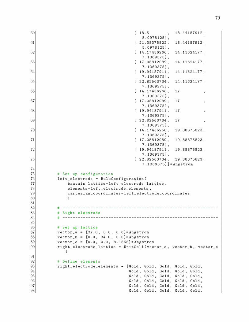
79
60 [ 18.5 , 18.44187912 ,
5.0978125] ,
61 [ 21.38375822 , 18.44187912 ,
5.0978125] ,
62 [ 14.17436266 , 14.11624177 ,
7.1369375] ,
63 [ 17.05812089 , 14.11624177 ,
7.1369375] ,
64 [ 19.94187911 , 14.11624177 ,
7.1369375] ,
65 [ 22.82563734 , 14.11624177 ,
7.1369375] ,
66 [ 14.17436266 , 17. ,
7.1369375] ,
67 [ 17.05812089 , 17. ,
7.1369375] ,
68 [ 19.94187911 , 17. ,
7.1369375] ,
69 [ 22.82563734 , 17. ,
7.1369375] ,
70 [ 14.17436266 , 19.88375823 ,
7.1369375] ,
71 [ 17.05812089 , 19.88375823 ,
7.1369375] ,
72 [ 19.94187911 , 19.88375823 ,
7.1369375] ,
73 [ 22.82563734 , 19.88375823 ,
7.1369375]]* Angstrom
7475 # Set up configuration
76 left_electrode = BulkConfiguration(
77 bravais_lattice=left_electrode_lattice ,
78 elements=left_electrode_elements ,
79 cartesian_coordinates=left_electrode_coordinates
80 )
8182 # -------------------------------------------------------------
83 # Right electrode
84 # -------------------------------------------------------------
8586 # Set up lattice
87 vector_a = [37.0 , 0.0, 0.0]* Angstrom
88 vector_b = [0.0, 34.0, 0.0]* Angstrom
89 vector_c = [0.0, 0.0, 8.1565]* Angstrom
90 right_electrode_lattice = UnitCell(vector_a , vector_b , vector_c
)
9192 # Define elements
93 right_electrode_elements = [Gold , Gold , Gold , Gold , Gold ,
94 Gold , Gold , Gold , Gold , Gold ,
95 Gold , Gold , Gold , Gold , Gold ,
96 Gold , Gold , Gold , Gold , Gold ,
97 Gold , Gold , Gold , Gold , Gold ,
98 Gold , Gold , Gold , Gold , Gold ,
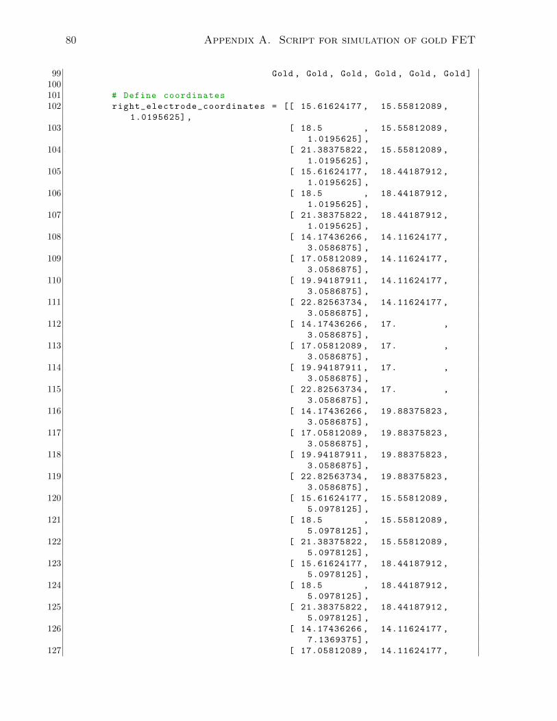
80 Appendix A. Script for simulation of gold FET
99 Gold , Gold , Gold , Gold , Gold , Gold]
100101 # Define coordinates
102 right_electrode_coordinates = [[ 15.61624177 , 15.55812089 ,
1.0195625] ,
103 [ 18.5 , 15.55812089 ,
1.0195625] ,
104 [ 21.38375822 , 15.55812089 ,
1.0195625] ,
105 [ 15.61624177 , 18.44187912 ,
1.0195625] ,
106 [ 18.5 , 18.44187912 ,
1.0195625] ,
107 [ 21.38375822 , 18.44187912 ,
1.0195625] ,
108 [ 14.17436266 , 14.11624177 ,
3.0586875] ,
109 [ 17.05812089 , 14.11624177 ,
3.0586875] ,
110 [ 19.94187911 , 14.11624177 ,
3.0586875] ,
111 [ 22.82563734 , 14.11624177 ,
3.0586875] ,
112 [ 14.17436266 , 17. ,
3.0586875] ,
113 [ 17.05812089 , 17. ,
3.0586875] ,
114 [ 19.94187911 , 17. ,
3.0586875] ,
115 [ 22.82563734 , 17. ,
3.0586875] ,
116 [ 14.17436266 , 19.88375823 ,
3.0586875] ,
117 [ 17.05812089 , 19.88375823 ,
3.0586875] ,
118 [ 19.94187911 , 19.88375823 ,
3.0586875] ,
119 [ 22.82563734 , 19.88375823 ,
3.0586875] ,
120 [ 15.61624177 , 15.55812089 ,
5.0978125] ,
121 [ 18.5 , 15.55812089 ,
5.0978125] ,
122 [ 21.38375822 , 15.55812089 ,
5.0978125] ,
123 [ 15.61624177 , 18.44187912 ,
5.0978125] ,
124 [ 18.5 , 18.44187912 ,
5.0978125] ,
125 [ 21.38375822 , 18.44187912 ,
5.0978125] ,
126 [ 14.17436266 , 14.11624177 ,
7.1369375] ,
127 [ 17.05812089 , 14.11624177 ,
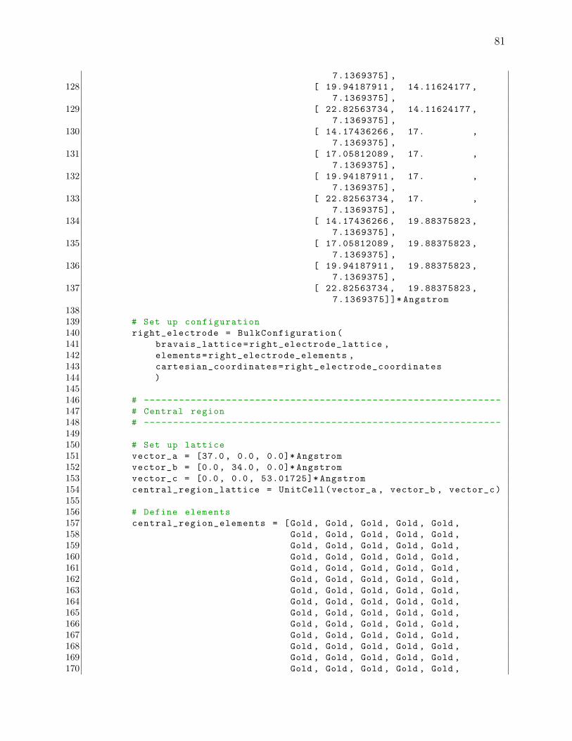
81
7.1369375] ,
128 [ 19.94187911 , 14.11624177 ,
7.1369375] ,
129 [ 22.82563734 , 14.11624177 ,
7.1369375] ,
130 [ 14.17436266 , 17. ,
7.1369375] ,
131 [ 17.05812089 , 17. ,
7.1369375] ,
132 [ 19.94187911 , 17. ,
7.1369375] ,
133 [ 22.82563734 , 17. ,
7.1369375] ,
134 [ 14.17436266 , 19.88375823 ,
7.1369375] ,
135 [ 17.05812089 , 19.88375823 ,
7.1369375] ,
136 [ 19.94187911 , 19.88375823 ,
7.1369375] ,
137 [ 22.82563734 , 19.88375823 ,
7.1369375]]* Angstrom
138139 # Set up configuration
140 right_electrode = BulkConfiguration(
141 bravais_lattice=right_electrode_lattice ,
142 elements=right_electrode_elements ,
143 cartesian_coordinates=right_electrode_coordinates
144 )
145146 # -------------------------------------------------------------
147 # Central region
148 # -------------------------------------------------------------
149150 # Set up lattice
151 vector_a = [37.0 , 0.0, 0.0]* Angstrom
152 vector_b = [0.0, 34.0, 0.0]* Angstrom
153 vector_c = [0.0, 0.0, 53.01725]* Angstrom
154 central_region_lattice = UnitCell(vector_a , vector_b , vector_c)
155156 # Define elements
157 central_region_elements = [Gold , Gold , Gold , Gold , Gold ,
158 Gold , Gold , Gold , Gold , Gold ,
159 Gold , Gold , Gold , Gold , Gold ,
160 Gold , Gold , Gold , Gold , Gold ,
161 Gold , Gold , Gold , Gold , Gold ,
162 Gold , Gold , Gold , Gold , Gold ,
163 Gold , Gold , Gold , Gold , Gold ,
164 Gold , Gold , Gold , Gold , Gold ,
165 Gold , Gold , Gold , Gold , Gold ,
166 Gold , Gold , Gold , Gold , Gold ,
167 Gold , Gold , Gold , Gold , Gold ,
168 Gold , Gold , Gold , Gold , Gold ,
169 Gold , Gold , Gold , Gold , Gold ,
170 Gold , Gold , Gold , Gold , Gold ,
82 Appendix A. Script for simulation of gold FET
171 Gold , Gold , Gold , Gold , Gold ,
172 Gold , Gold , Gold , Gold , Gold ,
173 Gold , Gold , Gold , Gold , Gold ,
174 Gold , Gold , Gold , Gold , Gold ,
175 Gold , Gold , Gold , Gold , Gold ,
176 Gold , Gold , Gold , Gold , Gold ,
177 Gold , Gold , Gold , Gold , Gold ,
178 Gold , Gold , Gold , Gold , Gold ,
179 Gold , Gold , Gold , Gold , Gold ,
180 Gold , Gold , Gold , Gold , Gold ,
181 Gold , Gold , Gold , Gold , Gold ,
182 Gold , Gold , Gold , Gold , Gold ,
183 Gold , Gold , Gold , Gold , Gold ,
184 Gold , Gold , Gold , Gold , Gold ,
185 Gold , Gold , Gold , Gold , Gold ,
186 Gold , Gold , Gold , Gold , Gold ,
187 Gold , Gold , Gold , Gold , Gold ,
188 Gold , Gold , Gold , Gold , Gold ,
189 Gold , Gold , Gold , Gold , Gold ,
190 Gold , Gold , Gold , Gold , Gold ,
191 Gold , Gold , Gold , Gold , Gold ,
192 Gold , Gold , Gold , Gold , Gold ,
193 Gold , Gold , Gold , Gold , Gold ,
194 Gold , Gold , Gold , Gold , Gold ,
195 Gold , Gold , Gold , Gold , Gold ,
196 Gold , Gold , Gold , Gold , Gold ,
197 Gold , Gold , Gold , Gold , Gold ,
198 Gold , Gold , Gold , Gold , Gold ,
199 Gold , Gold , Gold , Gold , Gold ,
200 Gold , Gold , Gold , Gold , Gold ,
201 Gold , Gold , Gold , Gold , Gold ,
202 Gold , Gold , Gold , Gold , Gold ,
203 Gold , Gold , Gold , Gold]
204205 # Define coordinates
206 central_region_coordinates = [[ 15.61624177 , 15.55812089 ,
1.0195625] ,
207 [ 18.5 , 15.55812089 ,
1.0195625] ,
208 [ 21.38375822 , 15.55812089 ,
1.0195625] ,
209 [ 15.61624177 , 18.44187912 ,
1.0195625] ,
210 [ 18.5 , 18.44187912 ,
1.0195625] ,
211 [ 21.38375822 , 18.44187912 ,
1.0195625] ,
212 [ 14.17436266 , 14.11624177 ,
3.0586875] ,
213 [ 17.05812089 , 14.11624177 ,
3.0586875] ,
214 [ 19.94187911 , 14.11624177 ,
3.0586875] ,
215 [ 22.82563734 , 14.11624177 ,
83
3.0586875] ,
216 [ 14.17436266 , 17. ,
3.0586875] ,
217 [ 17.05812089 , 17. ,
3.0586875] ,
218 [ 19.94187911 , 17. ,
3.0586875] ,
219 [ 22.82563734 , 17. ,
3.0586875] ,
220 [ 14.17436266 , 19.88375823 ,
3.0586875] ,
221 [ 17.05812089 , 19.88375823 ,
3.0586875] ,
222 [ 19.94187911 , 19.88375823 ,
3.0586875] ,
223 [ 22.82563734 , 19.88375823 ,
3.0586875] ,
224 [ 15.61624177 , 15.55812089 ,
5.0978125] ,
225 [ 18.5 , 15.55812089 ,
5.0978125] ,
226 [ 21.38375822 , 15.55812089 ,
5.0978125] ,
227 [ 15.61624177 , 18.44187912 ,
5.0978125] ,
228 [ 18.5 , 18.44187912 ,
5.0978125] ,
229 [ 21.38375822 , 18.44187912 ,
5.0978125] ,
230 [ 14.17436266 , 14.11624177 ,
7.1369375] ,
231 [ 17.05812089 , 14.11624177 ,
7.1369375] ,
232 [ 19.94187911 , 14.11624177 ,
7.1369375] ,
233 [ 22.82563734 , 14.11624177 ,
7.1369375] ,
234 [ 14.17436266 , 17. ,
7.1369375] ,
235 [ 17.05812089 , 17. ,
7.1369375] ,
236 [ 19.94187911 , 17. ,
7.1369375] ,
237 [ 22.82563734 , 17. ,
7.1369375] ,
238 [ 14.17436266 , 19.88375823 ,
7.1369375] ,
239 [ 17.05812089 , 19.88375823 ,
7.1369375] ,
240 [ 19.94187911 , 19.88375823 ,
7.1369375] ,
241 [ 22.82563734 , 19.88375823 ,
7.1369375] ,
242 [ 15.61624177 , 15.55812089 ,
84 Appendix A. Script for simulation of gold FET
9.1760625] ,
243 [ 18.5 , 15.55812089 ,
9.1760625] ,
244 [ 21.38375822 , 15.55812089 ,
9.1760625] ,
245 [ 15.61624177 , 18.44187912 ,
9.1760625] ,
246 [ 18.5 , 18.44187912 ,
9.1760625] ,
247 [ 21.38375822 , 18.44187912 ,
9.1760625] ,
248 [ 14.17436266 , 14.11624177 ,
11.2151875] ,
249 [ 17.05812089 , 14.11624177 ,
11.2151875] ,
250 [ 19.94187911 , 14.11624177 ,
11.2151875] ,
251 [ 22.82563734 , 14.11624177 ,
11.2151875] ,
252 [ 14.17436266 , 17. ,
11.2151875] ,
253 [ 17.05812089 , 17. ,
11.2151875] ,
254 [ 19.94187911 , 17. ,
11.2151875] ,
255 [ 22.82563734 , 17. ,
11.2151875] ,
256 [ 14.17436266 , 19.88375823 ,
11.2151875] ,
257 [ 17.05812089 , 19.88375823 ,
11.2151875] ,
258 [ 19.94187911 , 19.88375823 ,
11.2151875] ,
259 [ 22.82563734 , 19.88375823 ,
11.2151875] ,
260 [ 15.61624177 , 15.55812089 ,
13.2543125] ,
261 [ 18.5 , 15.55812089 ,
13.2543125] ,
262 [ 21.38375822 , 15.55812089 ,
13.2543125] ,
263 [ 15.61624177 , 18.44187912 ,
13.2543125] ,
264 [ 18.5 , 18.44187912 ,
13.2543125] ,
265 [ 21.38375822 , 18.44187912 ,
13.2543125] ,
266 [ 14.17436266 , 14.11624177 ,
15.2934375] ,
267 [ 17.05812089 , 14.11624177 ,
15.2934375] ,
268 [ 19.94187911 , 14.11624177 ,
15.2934375] ,
269 [ 22.82563734 , 14.11624177 ,
85
15.2934375] ,
270 [ 14.17436266 , 17. ,
15.2934375] ,
271 [ 17.05812089 , 17. ,
15.2934375] ,
272 [ 19.94187911 , 17. ,
15.2934375] ,
273 [ 22.82563734 , 17. ,
15.2934375] ,
274 [ 14.17436266 , 19.88375823 ,
15.2934375] ,
275 [ 17.05812089 , 19.88375823 ,
15.2934375] ,
276 [ 19.94187911 , 19.88375823 ,
15.2934375] ,
277 [ 22.82563734 , 19.88375823 ,
15.2934375] ,
278 [ 15.61624177 , 15.55812089 ,
17.3325625] ,
279 [ 18.5 , 15.55812089 ,
17.3325625] ,
280 [ 21.38375822 , 15.55812089 ,
17.3325625] ,
281 [ 15.61624177 , 18.44187912 ,
17.3325625] ,
282 [ 18.5 , 18.44187912 ,
17.3325625] ,
283 [ 21.38375822 , 18.44187912 ,
17.3325625] ,
284 [ 14.17436266 , 14.11624177 ,
19.3716875] ,
285 [ 17.05812089 , 14.11624177 ,
19.3716875] ,
286 [ 19.94187911 , 14.11624177 ,
19.3716875] ,
287 [ 22.82563734 , 14.11624177 ,
19.3716875] ,
288 [ 14.17436266 , 17. ,
19.3716875] ,
289 [ 17.05812089 , 17. ,
19.3716875] ,
290 [ 19.94187911 , 17. ,
19.3716875] ,
291 [ 22.82563734 , 17. ,
19.3716875] ,
292 [ 14.17436266 , 19.88375823 ,
19.3716875] ,
293 [ 17.05812089 , 19.88375823 ,
19.3716875] ,
294 [ 19.94187911 , 19.88375823 ,
19.3716875] ,
295 [ 22.82563734 , 19.88375823 ,
19.3716875] ,
296 [ 15.61624177 , 15.55812089 ,
86 Appendix A. Script for simulation of gold FET
21.4108125] ,
297 [ 18.5 , 15.55812089 ,
21.4108125] ,
298 [ 21.38375822 , 15.55812089 ,
21.4108125] ,
299 [ 15.61624177 , 18.44187912 ,
21.4108125] ,
300 [ 18.5 , 18.44187912 ,
21.4108125] ,
301 [ 21.38375822 , 18.44187912 ,
21.4108125] ,
302 [ 14.17436266 , 14.11624177 ,
23.4499375] ,
303 [ 17.05812089 , 14.11624177 ,
23.4499375] ,
304 [ 19.94187911 , 14.11624177 ,
23.4499375] ,
305 [ 22.82563734 , 14.11624177 ,
23.4499375] ,
306 [ 14.17436266 , 17. ,
23.4499375] ,
307 [ 17.05812089 , 17. ,
23.4499375] ,
308 [ 19.94187911 , 17. ,
23.4499375] ,
309 [ 22.82563734 , 17. ,
23.4499375] ,
310 [ 14.17436266 , 19.88375823 ,
23.4499375] ,
311 [ 17.05812089 , 19.88375823 ,
23.4499375] ,
312 [ 19.94187911 , 19.88375823 ,
23.4499375] ,
313 [ 22.82563734 , 19.88375823 ,
23.4499375] ,
314 [ 15.61624177 , 15.55812089 ,
25.4890625] ,
315 [ 18.5 , 15.55812089 ,
25.4890625] ,
316 [ 21.38375822 , 15.55812089 ,
25.4890625] ,
317 [ 15.61624177 , 18.44187912 ,
25.4890625] ,
318 [ 18.5 , 18.44187912 ,
25.4890625] ,
319 [ 21.38375822 , 18.44187912 ,
25.4890625] ,
320 [ 14.17436266 , 14.11624177 ,
27.5281875] ,
321 [ 17.05812089 , 14.11624177 ,
27.5281875] ,
322 [ 19.94187911 , 14.11624177 ,
27.5281875] ,
323 [ 22.82563734 , 14.11624177 ,
87
27.5281875] ,
324 [ 14.17436266 , 17. ,
27.5281875] ,
325 [ 17.05812089 , 17. ,
27.5281875] ,
326 [ 19.94187911 , 17. ,
27.5281875] ,
327 [ 22.82563734 , 17. ,
27.5281875] ,
328 [ 14.17436266 , 19.88375823 ,
27.5281875] ,
329 [ 17.05812089 , 19.88375823 ,
27.5281875] ,
330 [ 19.94187911 , 19.88375823 ,
27.5281875] ,
331 [ 22.82563734 , 19.88375823 ,
27.5281875] ,
332 [ 15.61624177 , 15.55812089 ,
29.5673125] ,
333 [ 18.5 , 15.55812089 ,
29.5673125] ,
334 [ 21.38375822 , 15.55812089 ,
29.5673125] ,
335 [ 15.61624177 , 18.44187912 ,
29.5673125] ,
336 [ 18.5 , 18.44187912 ,
29.5673125] ,
337 [ 21.38375822 , 18.44187912 ,
29.5673125] ,
338 [ 14.17436266 , 14.11624177 ,
31.6064375] ,
339 [ 17.05812089 , 14.11624177 ,
31.6064375] ,
340 [ 19.94187911 , 14.11624177 ,
31.6064375] ,
341 [ 22.82563734 , 14.11624177 ,
31.6064375] ,
342 [ 14.17436266 , 17. ,
31.6064375] ,
343 [ 17.05812089 , 17. ,
31.6064375] ,
344 [ 19.94187911 , 17. ,
31.6064375] ,
345 [ 22.82563734 , 17. ,
31.6064375] ,
346 [ 14.17436266 , 19.88375823 ,
31.6064375] ,
347 [ 17.05812089 , 19.88375823 ,
31.6064375] ,
348 [ 19.94187911 , 19.88375823 ,
31.6064375] ,
349 [ 22.82563734 , 19.88375823 ,
31.6064375] ,
350 [ 15.61624177 , 15.55812089 ,
88 Appendix A. Script for simulation of gold FET
33.6455625] ,
351 [ 18.5 , 15.55812089 ,
33.6455625] ,
352 [ 21.38375822 , 15.55812089 ,
33.6455625] ,
353 [ 15.61624177 , 18.44187912 ,
33.6455625] ,
354 [ 18.5 , 18.44187912 ,
33.6455625] ,
355 [ 21.38375822 , 18.44187912 ,
33.6455625] ,
356 [ 14.17436266 , 14.11624177 ,
35.6846875] ,
357 [ 17.05812089 , 14.11624177 ,
35.6846875] ,
358 [ 19.94187911 , 14.11624177 ,
35.6846875] ,
359 [ 22.82563734 , 14.11624177 ,
35.6846875] ,
360 [ 14.17436266 , 17. ,
35.6846875] ,
361 [ 17.05812089 , 17. ,
35.6846875] ,
362 [ 19.94187911 , 17. ,
35.6846875] ,
363 [ 22.82563734 , 17. ,
35.6846875] ,
364 [ 14.17436266 , 19.88375823 ,
35.6846875] ,
365 [ 17.05812089 , 19.88375823 ,
35.6846875] ,
366 [ 19.94187911 , 19.88375823 ,
35.6846875] ,
367 [ 22.82563734 , 19.88375823 ,
35.6846875] ,
368 [ 15.61624177 , 15.55812089 ,
37.7238125] ,
369 [ 18.5 , 15.55812089 ,
37.7238125] ,
370 [ 21.38375822 , 15.55812089 ,
37.7238125] ,
371 [ 15.61624177 , 18.44187912 ,
37.7238125] ,
372 [ 18.5 , 18.44187912 ,
37.7238125] ,
373 [ 21.38375822 , 18.44187912 ,
37.7238125] ,
374 [ 14.17436266 , 14.11624177 ,
39.7629375] ,
375 [ 17.05812089 , 14.11624177 ,
39.7629375] ,
376 [ 19.94187911 , 14.11624177 ,
39.7629375] ,
377 [ 22.82563734 , 14.11624177 ,
89
39.7629375] ,
378 [ 14.17436266 , 17. ,
39.7629375] ,
379 [ 17.05812089 , 17. ,
39.7629375] ,
380 [ 19.94187911 , 17. ,
39.7629375] ,
381 [ 22.82563734 , 17. ,
39.7629375] ,
382 [ 14.17436266 , 19.88375823 ,
39.7629375] ,
383 [ 17.05812089 , 19.88375823 ,
39.7629375] ,
384 [ 19.94187911 , 19.88375823 ,
39.7629375] ,
385 [ 22.82563734 , 19.88375823 ,
39.7629375] ,
386 [ 15.61624177 , 15.55812089 ,
41.8020625] ,
387 [ 18.5 , 15.55812089 ,
41.8020625] ,
388 [ 21.38375822 , 15.55812089 ,
41.8020625] ,
389 [ 15.61624177 , 18.44187912 ,
41.8020625] ,
390 [ 18.5 , 18.44187912 ,
41.8020625] ,
391 [ 21.38375822 , 18.44187912 ,
41.8020625] ,
392 [ 14.17436266 , 14.11624177 ,
43.8411875] ,
393 [ 17.05812089 , 14.11624177 ,
43.8411875] ,
394 [ 19.94187911 , 14.11624177 ,
43.8411875] ,
395 [ 22.82563734 , 14.11624177 ,
43.8411875] ,
396 [ 14.17436266 , 17. ,
43.8411875] ,
397 [ 17.05812089 , 17. ,
43.8411875] ,
398 [ 19.94187911 , 17. ,
43.8411875] ,
399 [ 22.82563734 , 17. ,
43.8411875] ,
400 [ 14.17436266 , 19.88375823 ,
43.8411875] ,
401 [ 17.05812089 , 19.88375823 ,
43.8411875] ,
402 [ 19.94187911 , 19.88375823 ,
43.8411875] ,
403 [ 22.82563734 , 19.88375823 ,
43.8411875] ,
404 [ 15.61624177 , 15.55812089 ,
90 Appendix A. Script for simulation of gold FET
45.8803125] ,
405 [ 18.5 , 15.55812089 ,
45.8803125] ,
406 [ 21.38375822 , 15.55812089 ,
45.8803125] ,
407 [ 15.61624177 , 18.44187912 ,
45.8803125] ,
408 [ 18.5 , 18.44187912 ,
45.8803125] ,
409 [ 21.38375822 , 18.44187912 ,
45.8803125] ,
410 [ 14.17436266 , 14.11624177 ,
47.9194375] ,
411 [ 17.05812089 , 14.11624177 ,
47.9194375] ,
412 [ 19.94187911 , 14.11624177 ,
47.9194375] ,
413 [ 22.82563734 , 14.11624177 ,
47.9194375] ,
414 [ 14.17436266 , 17. ,
47.9194375] ,
415 [ 17.05812089 , 17. ,
47.9194375] ,
416 [ 19.94187911 , 17. ,
47.9194375] ,
417 [ 22.82563734 , 17. ,
47.9194375] ,
418 [ 14.17436266 , 19.88375823 ,
47.9194375] ,
419 [ 17.05812089 , 19.88375823 ,
47.9194375] ,
420 [ 19.94187911 , 19.88375823 ,
47.9194375] ,
421 [ 22.82563734 , 19.88375823 ,
47.9194375] ,
422 [ 15.61624177 , 15.55812089 ,
49.9585625] ,
423 [ 18.5 , 15.55812089 ,
49.9585625] ,
424 [ 21.38375822 , 15.55812089 ,
49.9585625] ,
425 [ 15.61624177 , 18.44187912 ,
49.9585625] ,
426 [ 18.5 , 18.44187912 ,
49.9585625] ,
427 [ 21.38375822 , 18.44187912 ,
49.9585625] ,
428 [ 14.17436266 , 14.11624177 ,
51.9976875] ,
429 [ 17.05812089 , 14.11624177 ,
51.9976875] ,
430 [ 19.94187911 , 14.11624177 ,
51.9976875] ,
431 [ 22.82563734 , 14.11624177 ,
91
51.9976875] ,
432 [ 14.17436266 , 17. ,
51.9976875] ,
433 [ 17.05812089 , 17. ,
51.9976875] ,
434 [ 19.94187911 , 17. ,
51.9976875] ,
435 [ 22.82563734 , 17. ,
51.9976875] ,
436 [ 14.17436266 , 19.88375823 ,
51.9976875] ,
437 [ 17.05812089 , 19.88375823 ,
51.9976875] ,
438 [ 19.94187911 , 19.88375823 ,
51.9976875] ,
439 [ 22.82563734 , 19.88375823 ,
51.9976875]]* Angstrom
440441 # Set up configuration
442 central_region = BulkConfiguration(
443 bravais_lattice=central_region_lattice ,
444 elements=central_region_elements ,
445 cartesian_coordinates=central_region_coordinates
446 )
447448 # Add metallic region
449 metallic_region_0 = BoxRegion(
450 v*Volt ,
451 xmin = 3.1744* Angstrom , xmax = 33.8256* Angstrom ,
452 ymin = 3.1162* Angstrom , ymax = 4.1162* Angstrom ,
453 zmin = 11.5* Angstrom , zmax = 41.5* Angstrom
454 )
455456 metallic_region_1 = BoxRegion(
457 v*Volt ,
458 xmin = 3.1744* Angstrom , xmax = 33.8256* Angstrom ,
459 ymin = 29.8838* Angstrom , ymax = 30.8838* Angstrom ,
460 zmin = 11.5* Angstrom , zmax = 41.5* Angstrom
461 )
462463 metallic_region_2 = BoxRegion(
464 v*Volt ,
465 xmin = 3.1744* Angstrom , xmax = 4.1744* Angstrom ,
466 ymin = 4.1162* Angstrom , ymax = 29.8838* Angstrom ,
467 zmin = 11.5* Angstrom , zmax = 41.5* Angstrom
468 )
469470 metallic_region_3 = BoxRegion(
471 v*Volt ,
472 xmin = 32.8256* Angstrom , xmax = 33.8256* Angstrom ,
473 ymin = 4.1162* Angstrom , ymax = 29.8838* Angstrom ,
474 zmin = 11.5* Angstrom , zmax = 41.5* Angstrom
475 )
476
92 Appendix A. Script for simulation of gold FET
477 metallic_regions = [metallic_region_0 , metallic_region_1 ,
metallic_region_2 , metallic_region_3]
478 central_region.setMetallicRegions(metallic_regions)
479480 # Add dielectric region
481 dielectric_region_0 = BoxRegion(
482 25,
483 xmin = 4.1744* Angstrom , xmax = 32.8256* Angstrom ,
484 ymin = 4.1162* Angstrom , ymax = 14.1162* Angstrom ,
485 zmin = 0*Angstrom , zmax = 53.0171* Angstrom
486 )
487488 dielectric_region_1 = BoxRegion(
489 25,
490 xmin = 4.1744* Angstrom , xmax = 32.8256* Angstrom ,
491 ymin = 19.8838* Angstrom , ymax = 29.8838* Angstrom ,
492 zmin = 0*Angstrom , zmax = 53.0171* Angstrom
493 )
494495 dielectric_region_2 = BoxRegion(
496 25,
497 xmin = 4.1744* Angstrom , xmax = 14.1744* Angstrom ,
498 ymin = 14.1162* Angstrom , ymax = 19.8838* Angstrom ,
499 zmin = 0*Angstrom , zmax = 53.0171* Angstrom
500 )
501502 dielectric_region_3 = BoxRegion(
503 25,
504 xmin = 22.8256* Angstrom , xmax = 32.8256* Angstrom ,
505 ymin = 14.1162* Angstrom , ymax = 19.8838* Angstrom ,
506 zmin = 0*Angstrom , zmax = 53.0171* Angstrom
507 )
508509 dielectric_regions = [dielectric_region_0 , dielectric_region_1 ,
dielectric_region_2 , dielectric_region_3]
510 central_region.setDielectricRegions(dielectric_regions)
511512 device_configuration = DeviceConfiguration(
513 central_region ,
514 [left_electrode , right_electrode]
515 )
516517 # -------------------------------------------------------------
518 # Calculator
519 # -------------------------------------------------------------
520 #----------------------------------------
521 # Basis Set
522 #----------------------------------------
523 basis_set = [
524 CerdaHuckelParameters.Gold_fcc_Basis ,
525 ]
526527 #----------------------------------------
528 # Numerical Accuracy Settings
93
529 #----------------------------------------
530 left_electrode_numerical_accuracy_parameters =
NumericalAccuracyParameters(
531 k_point_sampling =(3, 3, 100),
532 )
533534 right_electrode_numerical_accuracy_parameters =
NumericalAccuracyParameters(
535 k_point_sampling =(3, 3, 100),
536 )
537538 device_numerical_accuracy_parameters =
NumericalAccuracyParameters(
539 k_point_sampling =(3, 3, 100),
540 )
541542 #----------------------------------------
543 # Iteration Control Settings
544 #----------------------------------------
545 left_electrode_iteration_control_parameters =
IterationControlParameters ()
546547 right_electrode_iteration_control_parameters =
IterationControlParameters ()
548549 device_iteration_control_parameters =
IterationControlParameters ()
550551 #----------------------------------------
552 # Poisson Solver Settings
553 #----------------------------------------
554 left_electrode_poisson_solver = MultigridSolver(
555 boundary_conditions =[[ NeumannBoundaryCondition ,
NeumannBoundaryCondition],
556 [NeumannBoundaryCondition ,
NeumannBoundaryCondition],
557 [PeriodicBoundaryCondition ,
PeriodicBoundaryCondition ]]
558 )
559560 right_electrode_poisson_solver = MultigridSolver(
561 boundary_conditions =[[ NeumannBoundaryCondition ,
NeumannBoundaryCondition],
562 [NeumannBoundaryCondition ,
NeumannBoundaryCondition],
563 [PeriodicBoundaryCondition ,
PeriodicBoundaryCondition ]]
564 )
565566 device_poisson_solver = MultigridSolver(
567 boundary_conditions =[[ NeumannBoundaryCondition ,
NeumannBoundaryCondition],
568 [NeumannBoundaryCondition ,
NeumannBoundaryCondition],
94 Appendix A. Script for simulation of gold FET
569 [DirichletBoundaryCondition ,
DirichletBoundaryCondition ]]
570 )
571572 #----------------------------------------
573 # Electrode Calculators
574 #----------------------------------------
575 left_electrode_calculator = HuckelCalculator(
576 basis_set=basis_set ,
577 numerical_accuracy_parameters=
left_electrode_numerical_accuracy_parameters ,
578 iteration_control_parameters=
left_electrode_iteration_control_parameters ,
579 poisson_solver=left_electrode_poisson_solver ,
580 )
581582 right_electrode_calculator = HuckelCalculator(
583 basis_set=basis_set ,
584 numerical_accuracy_parameters=
right_electrode_numerical_accuracy_parameters ,
585 iteration_control_parameters=
right_electrode_iteration_control_parameters ,
586 poisson_solver=right_electrode_poisson_solver ,
587 )
588589 #----------------------------------------
590 # Device Calculator
591 #----------------------------------------
592 calculator = DeviceHuckelCalculator(
593 basis_set=basis_set ,
594 numerical_accuracy_parameters=
device_numerical_accuracy_parameters ,
595 iteration_control_parameters=
device_iteration_control_parameters ,
596 poisson_solver=device_poisson_solver ,
597 electrode_calculators=
598 [left_electrode_calculator , right_electrode_calculator
],
599 electrode_voltages =( 0.1*Volt , 0.0* Volt),
600 )
601602 device_configuration.setCalculator(calculator)
603 nlprint(device_configuration)
604 device_configuration.update ()
605 nlsave(filename , device_configuration)
606607 # -------------------------------------------------------------
608 # Transmission spectrum
609 # -------------------------------------------------------------
610 transmission_spectrum = TransmissionSpectrum(
611 configuration=device_configuration ,
612 energies=numpy.linspace (-2,2,101)*eV,
613 kpoints=MonkhorstPackGrid (1,1),
614 energy_zero_parameter=AverageFermiLevel ,
95
615 infinitesimal =0.001*eV,
616 self_energy_calculator=DirectSelfEnergy (),
617 )
618 nlsave(filename , transmission_spectrum)
619 nlprint(transmission_spectrum)


![[Chapter III] Basic Knowledge of Discrete Semiconductor ......transistors (IGBTs) Power transistors (2SAxx,2SBxx,2SCxx,2SDxx, TTAxx,TTBxx,TTCxx,TTDxx) Types of Transistors Transistors](https://img.pdfslide.us/doc/110x75/5e766014341a1a707d5f4c34/chapter-iii-basic-knowledge-of-discrete-semiconductor-transistors-igbts.jpg)