Embed Size (px)
Citation preview
SPECIFICATION
G070VTN01.0
7.0" - WVGA - LVDS
Version: 1.0
Date: 01.12.2013
Note: This specification is subject to change without prior notice
www.data-modul.com
G070VTN01.0 rev. 1.0
1/25
G070VTN01.0
Preliminary Specifications
Final Specifications
Module 7.0 Inch Color TFT-LCD
Model Name G070VTN01.0
Customer Date
Checked &
Approved by
Note: This Specification is subject to change without notice.
Approved by Date
Grace Hung 2013/12/02
Prepared by
Yilan Hsu 2013/12/02
Audio-Video Business Unit / AU Optronics corporation
AUO C
onfid
entia
l For
DATA
MODUL
Inte
rnal U
se O
nly / 2
013/
12/1
0
Data Modul AG - www.data-modul.com

G070VTN01.0 rev. 1.0
2/25
G070VTN01.0
Contents
1. Operating Precautions.....................................................................................5
2. General Description.........................................................................................6
2.1 Display Characteristics...........................................................................................................6
2.2 Optical Characteristics ...........................................................................................................7
3. Functional Block Diagram.............................................................................10
4. Absolute Maximum Ratings ..........................................................................11
4.1 Absolute Ratings of TFT LCD Module .................................................................................11
5. Electrical Characteristics ..............................................................................12
5.1 TFT LCD Module ..................................................................................................................12
5.2 Backlight Unit........................................................................................................................14
6. Signal Characteristic .....................................................................................15
6.1 Pixel Format Image ..............................................................................................................15
6.2 Signal Description ................................................................................................................16
6.4 The Input Data Format .........................................................................................................18
6.5 Interface Timing ....................................................................................................................19
6.6 Power ON/OFF Sequence ...................................................................................................20
7. Connector & Pin Assignment........................................................................21
7.1 TFT LCD Signal (CN1): LVDS Connector ...........................................................................21
7.2 LED Backlight Unit: LED Connector ....................................................................................21
8. Reliability Test Criteria ..................................................................................22
9. Mechanical Characteristics ...........................................................................23
9.1 LCM Outline Dimension .......................................................................................................23
10. Label and Packaging....................................................................................24
10.1 Shipping Label (on the rear side of TFT-LCD display) ......................................................24
10.2 Carton Package .................................................................................................................24
11 Safety.............................................................................................................25
11.1 Sharp Edge Requirements.................................................................................................25
11.2 Materials .............................................................................................................................25
11.3 Capacitors...........................................................................................................................25
11.4 National Test Lab Requirement..........................................................................................25
AUO C
onfid
entia
l For
DATA
MODUL
Inte
rnal U
se O
nly / 2
013/
12/1
0
Data Modul AG - www.data-modul.com
G070VTN01.0 rev. 1.0
3/25
G070VTN01.0
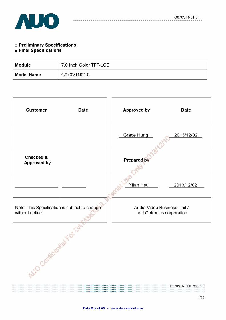
Record of Revision
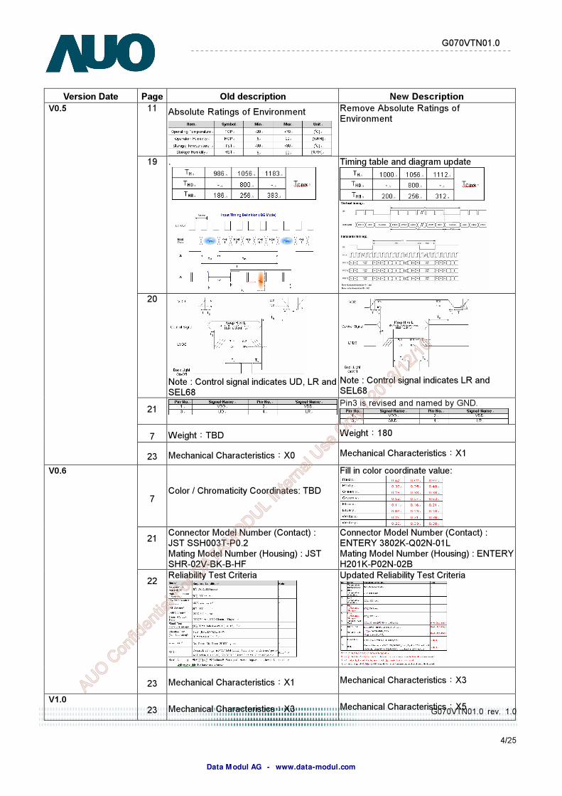
Version Date Page Old description New Description
V 0.2 20
22,23
LED Backlight Unit:
Original 2D outline
LED Backlight Unit:
Updated 2D outline including:
1. New 2D outline with mounting holes 2. New LED cable length defined
V 0.3 21 LED Cable Maker changed JST connector chosen
V 0.4 20
Note : Control signal indicates UD, LR and SEL68.
16
Pin3 is revised and named by GND.
V 0.5
17 The UD/RL pin setting should follow the
power on sequence in Section 6.6.
Fig. 1 Normal scan (Pin3, UD = Low or
NC ; Pin4, RL = Low or NC)
Fig. 2 Reverse scan (Pin3, UD = Low or
NC ; Pin4, RL = High)
Fig. 3 Reverse scan (Pin3, UD = High ;
Pin4, RL = Low or NC)
Fig. 4 Reverse scan (Pin3, UD = High ;
Pin4, RL = High)
The RL pin setting should follow the power
on sequence in Section 6.6.
Fig. 1 Normal scan (Pin4, RL = Low or NC)
Fig. 2 Reverse scan (Pin4, RL = High)
AUO C
onfid
entia
l For
DATA
MODUL
Inte
rnal U
se O
nly / 2
013/
12/1
0
Data Modul AG - www.data-modul.com
G070VTN01.0 rev. 1.0
4/25
G070VTN01.0
Version Date Page Old description New Description
11 Absolute Ratings of Environment
Remove Absolute Ratings of Environment
19 .
Timing table and diagram update
20
Note : Control signal indicates UD, LR and SEL68
Note : Control signal indicates LR and SEL68
21 Pin3 is revised and named by GND.
7 Weight:TBD Weight:180
V0.5
23 Mechanical Characteristics:X0 Mechanical Characteristics:X1
7 Color / Chromaticity Coordinates: TBD
Fill in color coordinate value:
21 Connector Model Number (Contact) : JST SSH003T-P0.2 Mating Model Number (Housing) : JST SHR-02V-BK-B-HF
Connector Model Number (Contact) : ENTERY 3802K-Q02N-01L Mating Model Number (Housing) : ENTERY H201K-P02N-02B
22 Reliability Test Criteria
Updated Reliability Test Criteria
V0.6
23 Mechanical Characteristics:X1 Mechanical Characteristics:X3
V1.0
23 Mechanical Characteristics:X3 Mechanical Characteristics:X5
AUO C
onfid
entia
l For
DATA
MODUL
Inte
rnal U
se O
nly / 2
013/
12/1
0
Data Modul AG - www.data-modul.com
G070VTN01.0 rev. 1.0
5/25
G070VTN01.0
1. Operating Precautions
1) Since front polarizer is easily damaged, please be cautious not to scratch it.
2) Be sure to turn off power supply when inserting or disconnecting from input connector.
3) Wipe off water drop immediately. Long contact with water may cause discoloration or spots.
4) When the panel surface is soiled, wipe it with absorbent cotton or soft cloth.
5) Since the panel is made of glass, it may be broken or cracked if dropped or bumped on hard
surface.
6) To avoid ESD (Electro Static Discharde) damage, be sure to ground yourself before handling
TFT-LCD Module.
7) Do not open nor modify the module assembly.
8) Do not press the reflector sheet at the back of the module to any direction.
9) In case if a module has to be put back into the packing container slot after it was taken out
from the container, do not press the center of the LED Reflector edge. Instead, press at the
far ends of the LED Reflector edge softly. Otherwise the TFT Module may be damaged.
10) At the insertion or removal of the Signal Interface Connector, be sure not to rotate nor tilt the
Interface Connector of the TFT Module.
11)After installation of the TFT Module into an enclosure (Notebook PC Bezel, for example), do
not twist nor bend the TFT Module even momentary. At designing the enclosure, it should be
taken into consideration that no bending/twisting forces are applied to the TFT Module from
outside. Otherwise the TFT Module may be damaged.
12) Small amount of materials having no flammability grade is used in the LCD module. The LCD
module should be supplied by power complied with requirements of Limited Power Source
(IEC60950 or UL1950), or be applied exemption.
13) Severe temperature condition may result in different luminance, response time.
14) Continuous operating TFT-LCD Module under high temperature environment may accelerate
LED light bar exhaustion and reduce luminance dramatically.
15) The data on this specification sheet is applicable when LCD module is placed in landscape
position.
16) Continuous displaying fixed pattern may induce image sticking. It is recommended to use
screen saver or shuffle content periodically if fixed pattern is displayed on the screen.
AUO C
onfid
entia
l For
DATA
MODUL
Inte
rnal U
se O
nly / 2
013/
12/1
0
Data Modul AG - www.data-modul.com
G070VTN01.0 rev. 1.0
6/25
G070VTN01.0
2. General Description
This specification applies to the 7.0 inch color TFT LCD module G070VTN01.0.
G070VTN01.0 is built in timing controller and LVDS interface. The screen format is intended to
support the WVGA (800(H) x 480(V)) screen and 16.2M (RGB 8-bits) or 262k colors (RGB
6-bits). G070VTN01.0 is a RoHS product.
2.1 Display Characteristics
The following items are characteristics summary on the table under 25 condition:
Items Unit Specifications
Screen Diagonal [inch] 7.0 ( 177.8mm )
Active Area [mm] 152.40(H) x 91.44(V)
Pixels H x V 800(H) x 480RGB(V)
Pixel Pitch [mm] 0.1905 x 0.1905
Pixel Arrangement R.G.B. Horizontal Stripe
Display Mode TN, Normally White
Nominal Input Voltage VDD [Volt] 3.3 typ.
LCD Typical Power Consumption [Watt] 0.33
Back Light Power Consumption [Watt] 1.47
Weight [Grams] 180
Physical Size [mm] 170.0(W) x 111.0(H) x 8.0(D) (typ.)
Electrical Interface 1 channel LVDS
Surface Treatment Anti-glare, Hardness 3H
Support Color 262K(6-bit) / 16.2M(8-bit)
Temperature Range Operating Storage (Non-Operating)
[oC]
[oC]
-20 to +70 -30 to +80
RoHS Compliance RoHS Compliance
AUO C
onfid
entia
l For
DATA
MODUL
Inte
rnal U
se O
nly / 2
013/
12/1
0
Data Modul AG - www.data-modul.com

G070VTN01.0 rev. 1.0
7/25
G070VTN01.0
2.2 Optical Characteristics The optical characteristics are measured under stable conditions at 25 (Room Temperature) :
Item Unit Conditions Min. Typ. Max. Note
White Luminance [cd/m2] IF= 20mA (center point) 250 300 - 1
Uniformity % 5 Points 1.3 1.2.3
Contrast Ratio 400 500 - 4
[msec] Rising - 12 20
[msec] Falling - 18 30 Response Time
[msec] Rising + Falling - 30 50
5
[degree] [degree]
Horizontal (Right) CR ≧ 10 (Left)
55
55
65
65
-
- Viewing Angle
[degree] [degree]
Vertical (Upper) CR ≧ 10 (Lower)
40
50
50
60
-
-
6
Red x 0.57 0.62 0.67
Red y 0.30 0.35 0.40
Green x 0.28 0.33 0.38
Green y 0.52 0.57 0.62
Blue x 0.11 0.16 0.21
Blue y 0.08 0.13 0.18
White x 0.26 0.31 0.36
Color / Chromaticity Coordinates (CIE 1931)
White y 0.28 0.33 0.38
1
Color Gamut % - 50 - 1
Note 1: Measurement method
Equipment: Pattern Generator, Power Supply, Digital Voltmeter, Luminance meter (SR_3 or equivalent)
Scanning Direction : Normal Scan
Aperture 1∘with 50cm viewing distance
Test Point Center,
Environment < 1 lux
LCD Module SR_3 or
equivalent
Measuring distance
Module Driving Equipment AUO C
onfid
entia
l For
DATA
MODUL
Inte
rnal U
se O
nly / 2
013/
12/1
0
Data Modul AG - www.data-modul.com
G070VTN01.0 rev. 1.0
8/25
G070VTN01.0
Note 2: Definition of 5 points position (Display active area: 152.40(H) x 91.44(V))
1 2
3
4 5
H /4
H /4
H /4
H /4
H
W
W /4 W /4 W /4 W /4
Note 3:
The luminance uniformity of 5 points is defined by dividing the maximum luminance value by the minimum luminance
value at full white condition.
Note 4: Definition of contrast ratio (CR):
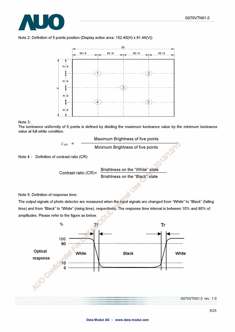
Note 5: Definition of response time:
The output signals of photo detector are measured when the input signals are changed from “White” to “Black” (falling
time) and from “Black” to “White” (rising time), respectively. The response time interval is between 10% and 90% of
amplitudes. Please refer to the figure as below.
Contrast ratio (CR)= Brightness on the “White” state
Brightness on the “Black” state
100 90
10 0
%
Optical
response White Black White
Tf Tr
90
10 0
Optical
response White Black White
Tr
Maximum Brightness of five points δW5 = Minimum Brightness of five points
AUO C
onfid
entia
l For
DATA
MODUL
Inte
rnal U
se O
nly / 2
013/
12/1
0
Data Modul AG - www.data-modul.com

G070VTN01.0 rev. 1.0
9/25
G070VTN01.0
Note 6: Definition of viewing angle
Viewing angle is the measurement of contrast ratio 10, at the screen center, over a 180° horizontal and 180° ≧
vertical range (off-normal viewing angles). The 180° viewing angle range is broken down as below: 90° (θ) horizontal
left and right, and 90° (Φ) vertical high (up) and low (down). The measurement direction is typically perpendicular to the
display surface with the screen rotated to its center to develop the desired measurement viewing angle.
AUO C
onfid
entia
l For
DATA
MODUL
Inte
rnal U
se O
nly / 2
013/
12/1
0
Data Modul AG - www.data-modul.com

G070VTN01.0 rev. 1.0
10/25
G070VTN01.0
3. Functional Block Diagram
The following diagram shows the functional block of the 7.0 inch color TFT/LCD module:
TFT-LCD
800*480(3) Pixels
Ga
te o
n A
rray
LVDS Receiver
Timing Controller
Source-Driver IC
LV
DS
Co
nn
ec
tor
LVDS
+ 3.3V
G1
D1
DC/DC
Converter
Gamma
Correction
LE
D C
on
ne
cto
r
+ 10.5V/140mA
AUO C
onfid
entia
l For
DATA
MODUL
Inte
rnal U
se O
nly / 2
013/
12/1
0
Data Modul AG - www.data-modul.com

G070VTN01.0 rev. 1.0
11/25
G070VTN01.0
4. Absolute Maximum Ratings
4.1 Absolute Ratings of TFT LCD Module
Item Symbol Min Max Unit Conditions
Logic/LCD Drive Voltage VDD -0.3 +3.6 [Volt]
AUO C
onfid
entia
l For
DATA
MODUL
Inte
rnal U
se O
nly / 2
013/
12/1
0
Data Modul AG - www.data-modul.com

G070VTN01.0 rev. 1.0
12/25
G070VTN01.0
5. Electrical Characteristics
5.1 TFT LCD Module
5.1.1 Power Specification
Symbol Parameter Min Typ Max Units Remark
VDD Logic/LCD Drive Voltage
3.0 3.3 3.6 [Volt] ±10%
IVDD VDD Current - 100 120 [mA] 64 Gray Bar Pattern
(VDD=3.3V, at 60Hz)
Irush LCD Inrush Current - - 1 [A] Note 1
PVDD VDD Power - 0.33 0.43 [Watt]
64 Gray Bar Pattern
(VDD=3.3V, at 60Hz)
Note 1: Measurement condition:
Q3
AO6402
G
D2
S
D1
D5
D6
Q3
AO6402
G
D2 S
D1
D5
D6
C11uF/16V
C2
1uF/25V
C3
0.01uF/25V
F1
VR1
47K
+12.0V
VCC
SW1
SW MAG-SPST
12
(High to Low)
Control
Signal
(LCD Module Input)
R2
1K
+3.3V
R1
47K
R2
1K
90%
10%
VDD rising time
0V
3.3V
470us
VDD
64 Gray pattern
AUO C
onfid
entia
l For
DATA
MODUL
Inte
rnal U
se O
nly / 2
013/
12/1
0
Data Modul AG - www.data-modul.com

G070VTN01.0 rev. 1.0
13/25
G070VTN01.0
5.1.2 Signal Electrical Characteristics Input signals shall be low or Hi-Z state when VDD is off.
Note: LVDS Signal Waveform.
Symbol Item Min. Typ. Max. Unit Remark
VTH Differential Input High Threshold - - 100 [mV] VICM=1.2V
VTL Differential Input Low Threshold -100 - - [mV] VICM=1.2V
|VID| Input Differential Voltage 100 400 600 [mV]
VICM Differential Input Common Mode Voltage 1.1 1.6 [V] VTH/VTL=±100mV
VICM
AUO C
onfid
entia
l For
DATA
MODUL
Inte
rnal U
se O
nly / 2
013/
12/1
0
Data Modul AG - www.data-modul.com

G070VTN01.0 rev. 1.0
14/25
G070VTN01.0
5.2 Backlight Unit
5.2.1 Parameter guideline for LED
Following characteristics are measured under a stable condition using an inverter at 25 (Room Temperature):The
backlight (LED module, Note 1) is suggested to drive by constant current 140mA.
Parameter Symbol Min. Typ. Max. Unit Remark
LED light bar Voltage VL 9.6 10.5 V IF=140mA
Power Consumption PBL 1.218 1.344 1.47 W Note 1
LED Life Time LL 30,000 -- -- Hr Note 2, 3
Note 1: The LED driving condition is defined for LED module (21 LED). The voltage range will be up to 10.5V based on
suggested driving current set as 140mA.
Note 2: Define “LED Lifetime”: brightness is decreased to 50% of the initial value. LED Lifetime is restricted under
normal condition, ambient temperature = 25 and LED light bar current = 140mA.
Note 3: If it uses larger LED light bar voltage/ current more than 10.5V/140mA, it maybe decreases the LED lifetime.
AUO C
onfid
entia
l For
DATA
MODUL
Inte
rnal U
se O
nly / 2
013/
12/1
0
Data Modul AG - www.data-modul.com

G070VTN01.0 rev. 1.0
15/25
G070VTN01.0
6. Signal Characteristic
6.1 Pixel Format Image
Following figure shows the relationship between input signal and LCD pixel format.
1 2 3
1st Line
2nd
Line
480th Line
AUO C
onfid
entia
l For
DATA
MODUL
Inte
rnal U
se O
nly / 2
013/
12/1
0
Data Modul AG - www.data-modul.com
G070VTN01.0 rev. 1.0
16/25
G070VTN01.0
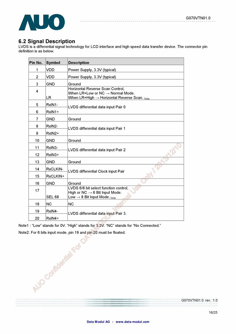
6.2 Signal Description LVDS is a differential signal technology for LCD interface and high speed data transfer device. The connector pin definition is as below.
Pin No. Symbol Description
1 VDD Power Supply, 3.3V (typical)
2 VDD Power Supply, 3.3V (typical)
3 GND Ground
4
LR
Horizontal Reverse Scan Control, When LR=Low or NC → Normal Mode. When LR=High → Horizontal Reverse Scan. Note
5 RxIN1-
6 RxIN1+ LVDS differential data input Pair 0
7 GND Ground
8 RxIN2-
9 RxIN2+ LVDS differential data input Pair 1
10 GND Ground
11 RxIN3-
12 RxIN3+ LVDS differential data input Pair 2
13 GND Ground
14 RxCLKIN-
15 RxCLKIN+ LVDS differential Clock input Pair
16 GND Ground
17
SEL 68
LVDS 6/8 bit select function control, High or NC → 6 Bit Input Mode. Low → 8 Bit Input Mode. Note
18 NC NC
19 RxIN4-
20 RxIN4+ LVDS differential data input Pair 3.
Note1 : “Low” stands for 0V. “High” stands for 3.3V. “NC” stands for “No Connected.”
Note2: For 6 bits input mode, pin 19 and pin 20 must be floated.
AUO C
onfid
entia
l For
DATA
MODUL
Inte
rnal U
se O
nly / 2
013/
12/1
0
Data Modul AG - www.data-modul.com
G070VTN01.0 rev. 1.0
17/25
G070VTN01.0
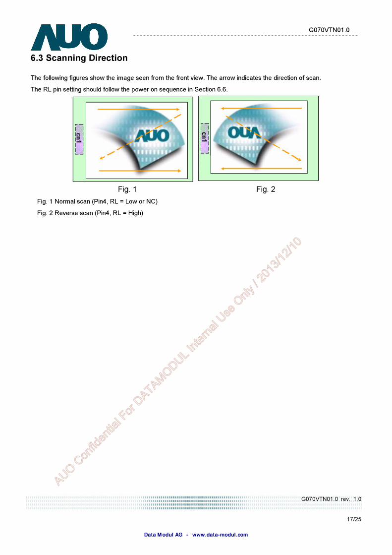
6.3 Scanning Direction
The following figures show the image seen from the front view. The arrow indicates the direction of scan.
The RL pin setting should follow the power on sequence in Section 6.6.
Fig. 1 Fig. 2
Fig. 1 Normal scan (Pin4, RL = Low or NC)
Fig. 2 Reverse scan (Pin4, RL = High)
AUO C
onfid
entia
l For
DATA
MODUL
Inte
rnal U
se O
nly / 2
013/
12/1
0
Data Modul AG - www.data-modul.com

G070VTN01.0 rev. 1.0
18/25
G070VTN01.0
6.4 The Input Data Format
6.4.1 SEL68
SEL68 = ” High” or “NC” for 6 bits LVDS Input
SEL68 = “Low” for 8 bits LVDS Input
Signal Name Description Remark
R7 R6 R5 R4 R3 R2 R1 R0
Red Data 7 (MSB) Red Data 6 Red Data 5 Red Data 4 Red Data 3 Red Data 2 Red Data 1 Red Data 0 (LSB)
Red-pixel Data Each red pixel’s brightness data consists of these 8 bits pixel data.
G7 G6 G5 G4 G3 G2 G1 G0
Green Data 7 (MSB) GreenData 6 GreenData 5 GreenData 4 GreenData 3 GreenData 2 GreenData 1 GreenData 0 (LSB)
Green-pixel Data Each green pixel’s brightness data consists of these 8 bits pixel data.
B7 B6 B5 B4 B3 B2 B1 B0
Blue Data 7 (MSB) Blue Data 6 Blue Data 5 Blue Data 4 Blue Data 3 Blue Data 2 Blue Data 1 Blue Data 0 (LSB)
Blue-pixel Data Each blue pixel’s brightness data consists of these 8 bits pixel data.
RxCLKIN+ RxCLKIN-
LVDS Clock Input
DE Display Enable
RSV Reserved Signal “High” or “Low” is acceptable
Note: Output signals from any system shall be low or Hi-Z state when VDD is off.
AUO C
onfid
entia
l For
DATA
MODUL
Inte
rnal U
se O
nly / 2
013/
12/1
0
Data Modul AG - www.data-modul.com

G070VTN01.0 rev. 1.0
19/25
G070VTN01.0
6.5 Interface Timing
6.5.1 Timing Characteristics
DE mode only
Parameter Symbol Min. Typ. Max. Unit Condition
Clock frequency 1/ TClock 30.3 33.26 37.8 MHz
Period TV 517 525 532
Active TVD - 480 - Vertical
Section
Blanking TVB 37 45 52
TH
Period TH 1000 1056 1112
Active THD - 800 - Horizontal
Section
Blanking THB 200 256 312
TClock
Note: Frame rate is 60 Hz.
6.5.2 Input Timing Diagram
Vertical timing:
Horizontal timing:
AUO C
onfid
entia
l For
DATA
MODUL
Inte
rnal U
se O
nly / 2
013/
12/1
0
Data Modul AG - www.data-modul.com
G070VTN01.0 rev. 1.0
20/25
G070VTN01.0
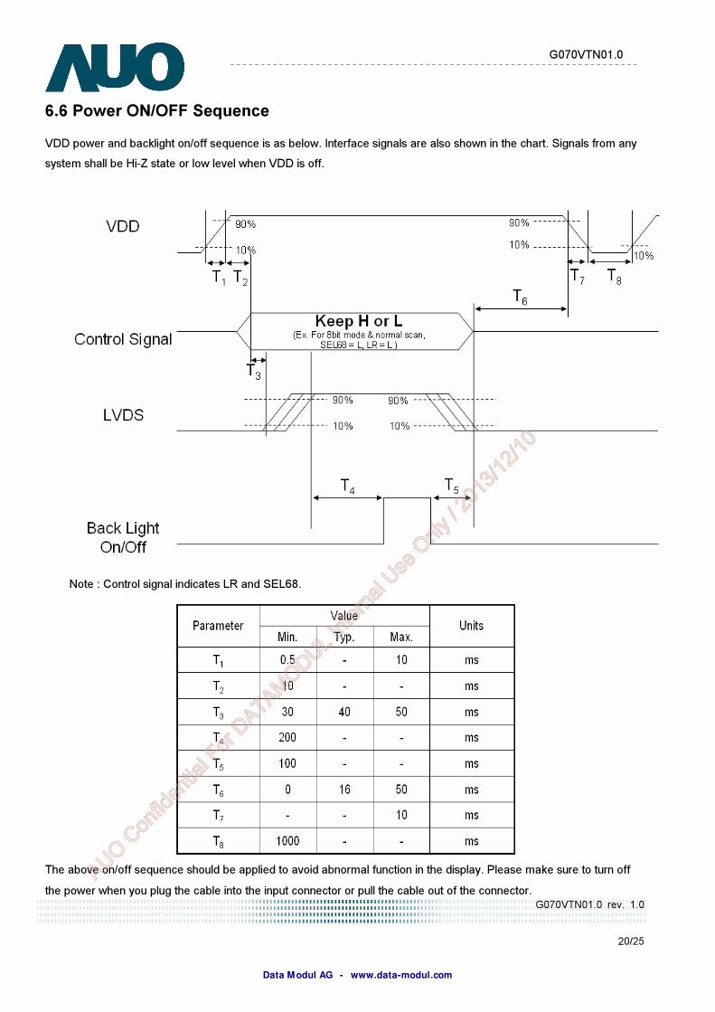
6.6 Power ON/OFF Sequence VDD power and backlight on/off sequence is as below. Interface signals are also shown in the chart. Signals from any
system shall be Hi-Z state or low level when VDD is off.
Note : Control signal indicates LR and SEL68.
The above on/off sequence should be applied to avoid abnormal function in the display. Please make sure to turn off
the power when you plug the cable into the input connector or pull the cable out of the connector. AUO C
onfid
entia
l For
DATA
MODUL
Inte
rnal U
se O
nly / 2
013/
12/1
0
Data Modul AG - www.data-modul.com
G070VTN01.0 rev. 1.0
21/25
G070VTN01.0
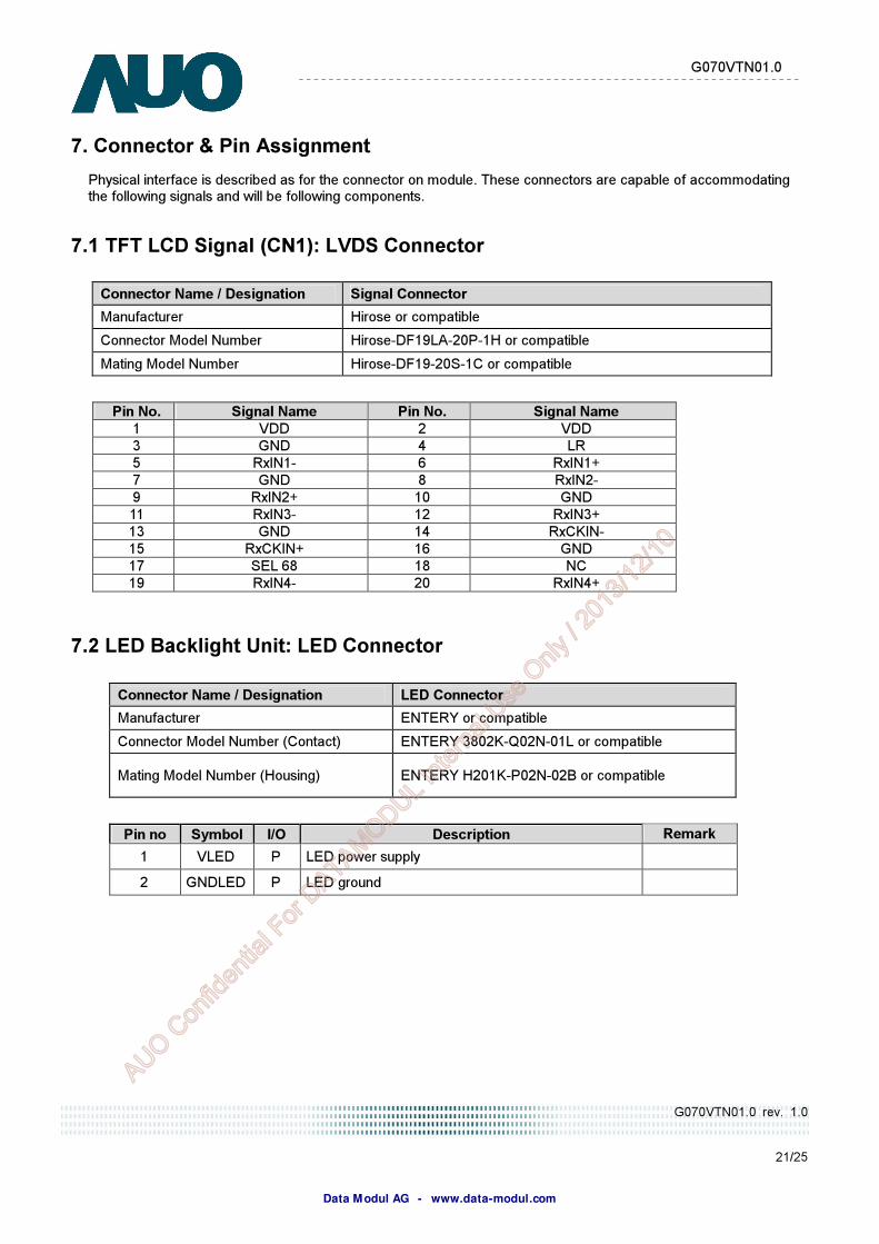
7. Connector & Pin Assignment
Physical interface is described as for the connector on module. These connectors are capable of accommodating the following signals and will be following components.
7.1 TFT LCD Signal (CN1): LVDS Connector
Connector Name / Designation Signal Connector
Manufacturer Hirose or compatible
Connector Model Number Hirose-DF19LA-20P-1H or compatible
Mating Model Number Hirose-DF19-20S-1C or compatible
Pin No. Signal Name Pin No. Signal Name
1 VDD 2 VDD
3 GND 4 LR
5 RxIN1- 6 RxIN1+
7 GND 8 RxIN2-
9 RxIN2+ 10 GND
11 RxIN3- 12 RxIN3+
13 GND 14 RxCKIN-
15 RxCKIN+ 16 GND
17 SEL 68 18 NC
19 RxIN4- 20 RxIN4+
7.2 LED Backlight Unit: LED Connector
Connector Name / Designation LED Connector
Manufacturer ENTERY or compatible
Connector Model Number (Contact) ENTERY 3802K-Q02N-01L or compatible
Mating Model Number (Housing) ENTERY H201K-P02N-02B or compatible
Pin no Symbol I/O Description Remark
1 VLED P LED power supply
2 GNDLED P LED ground
AUO C
onfid
entia
l For
DATA
MODUL
Inte
rnal U
se O
nly / 2
013/
12/1
0
Data Modul AG - www.data-modul.com

G070VTN01.0 rev. 1.0
22/25
G070VTN01.0
8. Reliability Test Criteria
No Items Required Condition Note
1 Temperature
Humidity Bias 40 /90%,300 hours
2 High
Temperature
Operation 70 ,300 hours
3 Low
Temperature
Operation -20 ,300 hours
4 High
Temperature
Storage 80 ,300 hours
5 Low
Temperature
Storage -30 ,300 hours
6 Thermal Shock
Test -20 /30 min ,60 /30 min ,100cycles (Non-Operating)
7 Shock Test 50G,20ms,Half-sine wave,( ±X, ±Y, ±Z) (Non-Operating)
8
Vibration Test 1.5G, (10~200~10Hz, P-P)
30 mins/axis (X, Y, Z) (Non-Operating)
9 On/off test On/10 sec, Off/10 sec, 30,000 cycles Note 3
10
ESD Contact Discharge: ± 8KV, 150pF(330Ω ) 1sec, 8 points, 25 times/ point
Air Discharge: ± 15KV, 150pF(330Ω ) 1sec, 8 points, 25 times/ point Note 4
Note 1: (for test item 1 to 6) Ta: Ambient temperature
Note 2: (for test item 1 to 6) Test method: check with recovery time 2hrs in the laboratory environment.
Note 3: Judged by the on/off testing results of AUO’s standard w/o functional fail.
Note 4: According to EN61000-4-2, ESD class B: Some performance degradation allowed. No data lost
. Self-recoverable. No hardware failures.
AUO C
onfid
entia
l For
DATA
MODUL
Inte
rnal U
se O
nly / 2
013/
12/1
0
Data Modul AG - www.data-modul.com
G070VTN01.0 rev. 1.0
23/25
G070VTN01.0
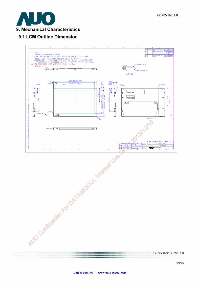
9. Mechanical Characteristics
9.1 LCM Outline Dimension
AUO C
onfid
entia
l For
DATA
MODUL
Inte
rnal U
se O
nly / 2
013/
12/1
0
Data Modul AG - www.data-modul.com

G070VTN01.0 rev. 1.0
24/25
G070VTN01.0
10. Label and Packaging
10.1 Shipping Label (on the rear side of TFT-LCD display)
10.2 Carton Package
Note:
1. Max. Capacity: 60pcs LCD Modules / per carton
2. Max. Weight: 14.4 kg / per carton
3. The outside dimension of carton is 434(L) mm x 377(W) mm x 264(H) mm
G070VTN01.0
AUO C
onfid
entia
l For
DATA
MODUL
Inte
rnal U
se O
nly / 2
013/
12/1
0
Data Modul AG - www.data-modul.com
G070VTN01.0 rev. 1.0
25/25
G070VTN01.0
11 Safety
11.1 Sharp Edge Requirements
There will be no sharp edges or corners on the display assembly that could cause injury.
11.2 Materials
11.2.1 Toxicity
There will be no carcinogenic materials used anywhere in the display module. If toxic materials are used,
they will be reviewed and approved by the responsible AUO toxicologist.
11.2.2 Flammability
All components including electrical components that do not meet the flammability grade UL94-V1 in the
module will complete the flammability rating exception approval process.
The pRxINted circuit board will be made from material rated 94-V1 or better. The actual UL flammability
rating will be pRxINted on the pRxINted circuit board.
11.3 Capacitors
If any polarized capacitors are used in the display assembly, provisions will be made to keep them from
being inserted backwards.
11.4 National Test Lab Requirement The display module will satisfy all requirements for compliance to:
UL 1950, First Edition U.S.A. Information Technology Equipment
AUO C
onfid
entia
l For
DATA
MODUL
Inte
rnal U
se O
nly / 2
013/
12/1
0
Data Modul AG - www.data-modul.com

ALL TECHNOLOGIES. ALL COMPETENCIES. ONE SPECIALIST.
DATA MODUL AG
Landsberger Straße 322
DE-80687 Munich
Phone: +49-89-56017-0
DATA MODUL WEIKERSHEIM GMBH
Lindenstraße 8
DE-97990 Weikersheim
Phone: +49-7934-101-0
More information and worldwide locations can be found at
www.data-modul .com


![Jst Bst: [Portfolio]](https://img.pdfslide.us/doc/110x75/55a446251a28abf32b8b46f8/jst-bst-portfolio-55a5186eb3369.jpg)