Embed Size (px)
Citation preview

8/4/2019 BwEE2601-13_BJT and FET Frequency Response
http://slidepdf.com/reader/full/bwee2601-13bjt-and-fet-frequency-response 1/15
1
13. BJT and FET FrequencyResponse
13.1 Decibel Unit (dB)
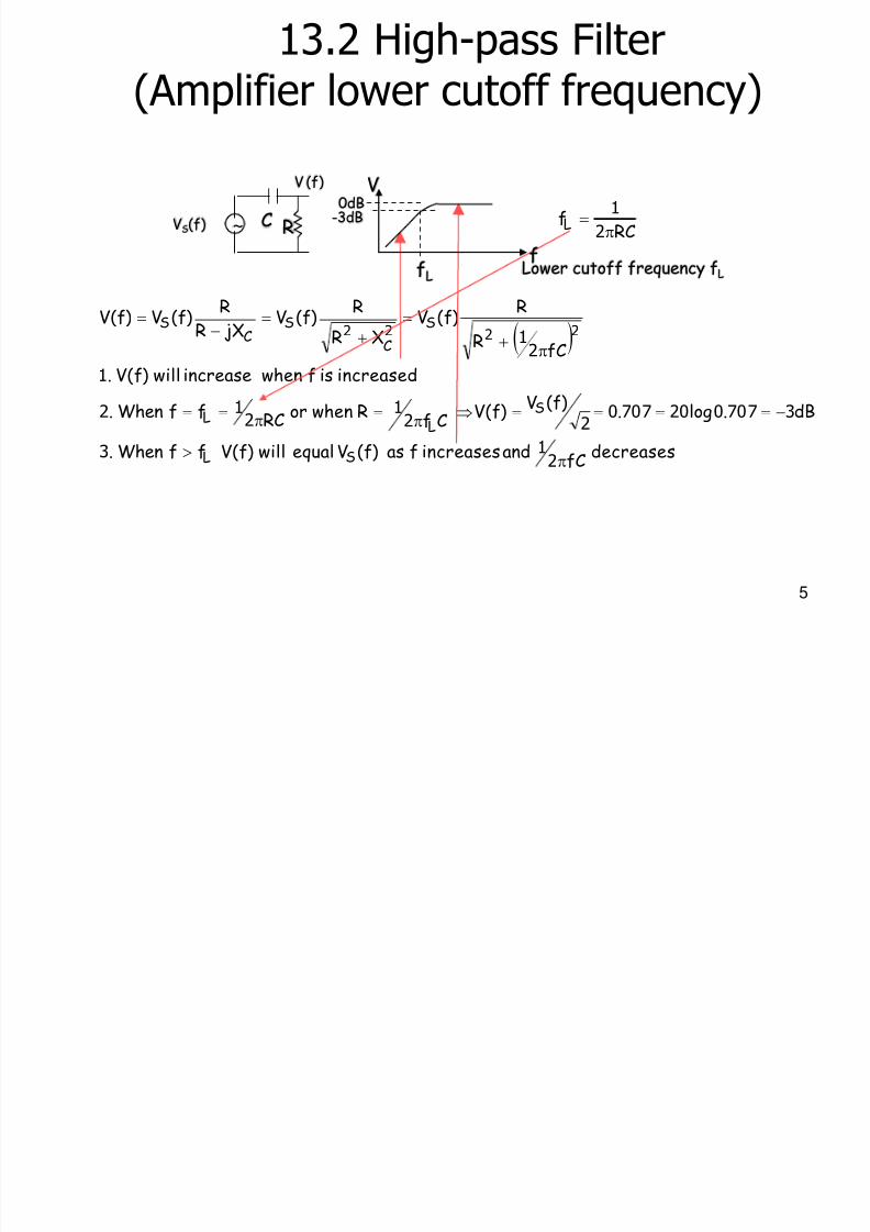
13.2 High-pass Filter (Amplifier lower cutoff frequency=f L)
13.3 Low-pass Filter (Amplifier higher cutoff frequency=f H)
13.4 Pass-band of BJT Amplifier
13.5 Pass-band of FET Amplifier

8/4/2019 BwEE2601-13_BJT and FET Frequency Response
http://slidepdf.com/reader/full/bwee2601-13bjt-and-fet-frequency-response 2/15
2
13.1 Decibel Unit (dB)dB is an electrical unit used in Electronic engineering. They provide a lot of
easiness in understanding on the performance of the systems.
dB is the 10 times logarithm of a power ratio dB = 10 log(P1/P2)
Since P= V2/R then dB=10log(P1/P2)=10log(V12/R)/(V2
2/R)=10log(V12/V2
2)=20log(V1/V2)
Since P= I2 R then dB=10log(P1/P2)=10log(I12R/I2
2R)=10log(I1/I2)2= 20log(I1/I2)
Then dB is the 20 times logarithm of a voltage ratio or current ratio.
AV=10
Amplifier1mV 10mV
Voltage ratio
Amplifier1mV 10mV
(AV)dB=20log10=20dB
dB
(AV)dB=20 log (10mV/1mV)=20 log10=20dB
Voltage Gain of the amplifier is 10 or 20dB
Amplifier1mV 10mV
AV=10mV/1mV=10
Vin Vo

8/4/2019 BwEE2601-13_BJT and FET Frequency Response
http://slidepdf.com/reader/full/bwee2601-13bjt-and-fet-frequency-response 3/15
3
AP=200
Amplifier1mW 200mW
Power ratio
Amplifier
1mW 200mW
(AP)dB=10log200=23dB
dB
(AP)dB=10 log (100mW/1mW)=10 log100=20dB
Power Gain of the amplifier is 200 or 23dB

8/4/2019 BwEE2601-13_BJT and FET Frequency Response
http://slidepdf.com/reader/full/bwee2601-13bjt-and-fet-frequency-response 4/15
4
Total Voltage Gain of the system is 100 or 40dB
Amplifier 20mV
(AV2)dB=20log2=6dB AV2=2 AV1=10
Amplifier 1mV 10mV
Voltage ratio (AV1)dB=20log10=20dB dB
Amplifier AV3=5
100mV
(AV3)dB=20log5=14dB
AVT =10x2x5=100 Multiply the ratio for total Voltage Gain
(AVT )dB=20+6+14=40dB Add the dB for total Voltage Gain in dB
(AVT )dB=20log100=40dB
Or find dB from the ratio for total Voltage Gain in dB
8/4/2019 BwEE2601-13_BJT and FET Frequency Response
http://slidepdf.com/reader/full/bwee2601-13bjt-and-fet-frequency-response 5/15
5
decreasesfCandincreasesfas)f(Vequalwill)f(VffWhen.
dB.log.)f(V)f(VCfRwhenorRCffWhen.
increasedisfwhenincreasewill)f(V.
fCR
R)f(V
XR
R)f(V
jXR
R)f(V)f(V
SL
SL
L
S
C
SC
S
213
3707020707022
12
12
1
21
2222
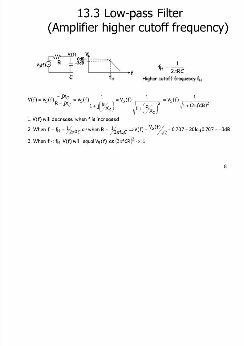
13.2 High-pass Filter(Amplifier lower cutoff frequency)
RCfL
2
1
f
V
R
C ~VS(f)
fLLower cutoff frequency fL
V (f)
0dB
-3dB

8/4/2019 BwEE2601-13_BJT and FET Frequency Response
http://slidepdf.com/reader/full/bwee2601-13bjt-and-fet-frequency-response 6/15
6
•All types of BJT amplifier circuits have a high pass filter at the place where coupling andbypass capacitors are used
VCC
RL
Ri
CC
CB
vi
R2
R1
RE
vo
RoRin
vin
iin
iL
Emitter Follower
VCC
RC
RL
CE
Ri CCCB
vi
R2
R1 RE
vo
Common Emitter
At lower frequencies, Reactance of bypass capacitor becomes higher (open) and the CE
amplifier behave as CE with RE whose voltage gain becomes smaller
RCfL 2
1
f
V
R
C ~VS(f)
fLLower cutoff frequency fL
V (f)
0dB
-3dB

8/4/2019 BwEE2601-13_BJT and FET Frequency Response
http://slidepdf.com/reader/full/bwee2601-13bjt-and-fet-frequency-response 7/15
7
1CL1L CRR2
1f
6dB/octave
12dB/octave
18dB/octave
fL1= fL2= fLE
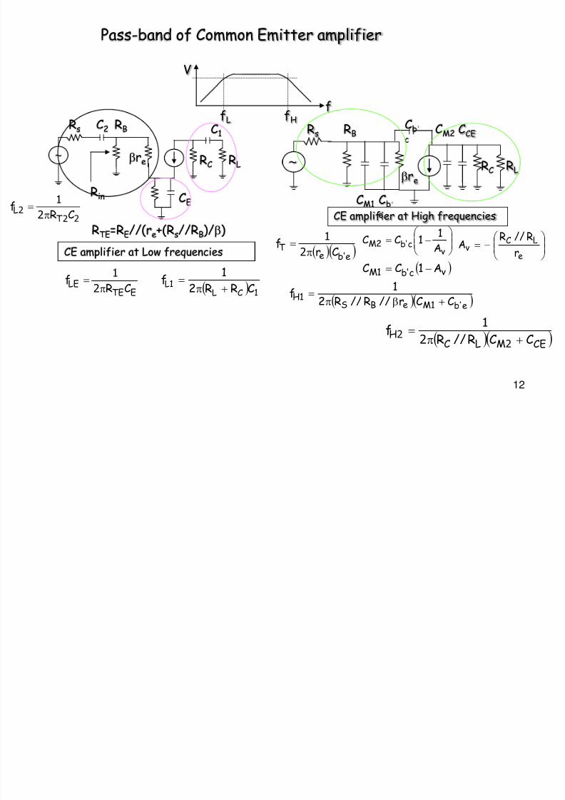
Overall Lower frequency response of Common Emitter amplifier
If fL1= fL2= fLE
18dB/octave
at Mid-frequencies
fL1
fL2fLE
CE amplifier at Low frequencies
RLbre
Rs
Rin
C1C2
RTE
= RE
//(re
+(Rs
//RB
)/b)
CE
~
RB
RC
E TE LE
C R 2 1 f
2 2 T 2 L
C R 2
1 f
RT2=Rs+(RB//(bre))
Assume all capacitorsshort when consideringone capacitor
f
V
fLEfL2fL1
8/4/2019 BwEE2601-13_BJT and FET Frequency Response
http://slidepdf.com/reader/full/bwee2601-13bjt-and-fet-frequency-response 8/15
8
13.3 Low-pass Filter(Amplifier higher cutoff frequency)
123
3707020707022
12
12
1
21
1
1
1
1
1
2
22
fCRas)f(Vequalwill)f(VffWhen.
dB.log.)f(V)f(VCfRwhenorRCffWhen.
increasedisfwhendecreasewill)f(V.
fCR)f(V
XR
)f(V
XR j
)f(V jXR
jX)f(V)f(V
SH
SH
H
S
C
S
C
SC
CS
RCfH
2
1
Higher cutoff frequency fH
f fHC
R
V V (f)
0dB -3dB ~VS(f)
8/4/2019 BwEE2601-13_BJT and FET Frequency Response
http://slidepdf.com/reader/full/bwee2601-13bjt-and-fet-frequency-response 9/15
9
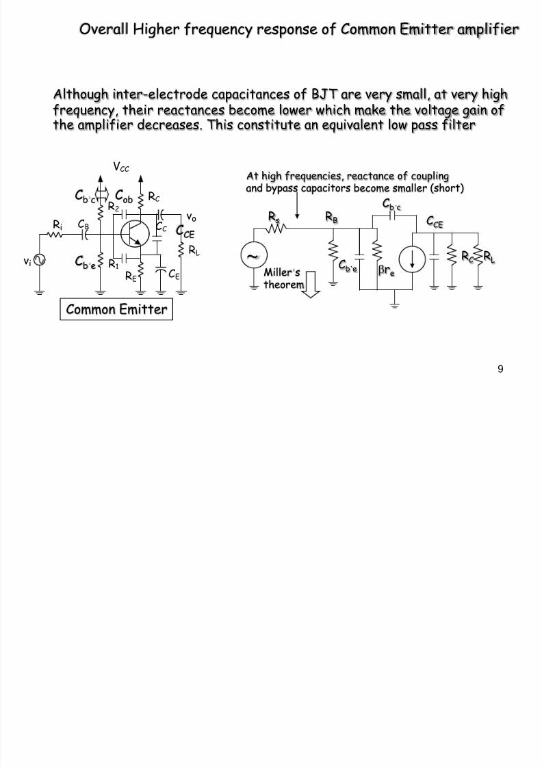
Although inter-electrode capacitances of BJT are very small, at very highfrequency, their reactances become lower which make the voltage gain ofthe amplifier decreases. This constitute an equivalent low pass filter
RLbre
Rs CCE
Cb’e~
RB
RC
Cb’c
At high frequencies, reactance of coupling
and bypass capacitors become smaller (short)
Miller’
stheorem
VCC
RC
RL
CE
Ri CCCB
vi
R2
R1
RE
vo
Common Emitter
Cb’e
CCE
Cb’c Cob
Overall Higher frequency response of Common Emitter amplifier

8/4/2019 BwEE2601-13_BJT and FET Frequency Response
http://slidepdf.com/reader/full/bwee2601-13bjt-and-fet-frequency-response 10/15
10
fH2fH1 CE amplifier at High frequencies
RLbre
Rs CCE
Cb’e
~
RB
RC
CM1
CM2
Cb’c
e'b1MeBS1H CCr//R//R2
1f
b
CE2MLC2H CCR//R2
1f
Miller’s theorem v1M
v1Mv1M A1CC
A1C j
1
C j
1
A1
ZZ
vc'b1M A1CC
vc'b2M A
11CC
e
LCv
r
R//RA
CE amplifier at Highfrequencies
RLbre
Rs CCE
Cb’e
~
RB
RC
CM1
CM2
Cb’
c
f
V
fH1f
V
fH2

8/4/2019 BwEE2601-13_BJT and FET Frequency Response
http://slidepdf.com/reader/full/bwee2601-13bjt-and-fet-frequency-response 11/15
11
f
V
fL fH
CE amplifier at High frequencies
RLbre
Rs CCE
Cb’e
~
RB
RC
CM1
CM2Cb’
c
CE amplifier at Low frequencies
RLbre
Rs
Rin
C1C2
RTE=RE//(re+(Rs//RB)/b)
CE
~
RB
RC
f
V
fH
13.4 Pass-band of BJT Amplifier
f
V
fL
8/4/2019 BwEE2601-13_BJT and FET Frequency Response
http://slidepdf.com/reader/full/bwee2601-13bjt-and-fet-frequency-response 12/15
12
f
V
fL fH
CE amplifier at High frequencies
RLbre
Rs CCE
Cb’
e
~
RB
RC
CM1
CM2Cb’
c
CE amplifier at Low frequencies
RLbre
Rs
Rin
C1C2
RTE=RE//(re+(Rs//RB)/b)
CE
~
RB
RC
ETELE
CR
f
2
1
22
22
1
CRf
T L
1CL1L
CRR2
1f
e'beT Crf
2
1
vc'b2M A
11CC
e
LCv
r
R//RA
vc'b1M A1CC
CEMLCH CCR//Rf
22
2
1
e'b1MeBS1H CCr//R//R2 1f b
Pass-band of Common Emitter amplifier

8/4/2019 BwEE2601-13_BJT and FET Frequency Response
http://slidepdf.com/reader/full/bwee2601-13bjt-and-fet-frequency-response 13/15
13
13.5 Pass-band of FET Amplifier
•All types of FET amplifier circuits have a high pass filter at the place where coupling andbypass capacitors are used
VDD
RD
RL
CS
Ri CCCG
vi
RG RS
vo
Common Source Amplifier
RC 2 1 f L
f
V
R C ~f
fLLower cutoff frequency fL
At lower frequencies, Reactance of bypass capacitor becomes higher (open) and the CS
amplifier behave as CS with RS whose voltage gain becomes smaller
Overall Lower frequency response of Common Source amplifier
STSLS CR
f
2
1
GiGL
CRRf 2
12
CDLL CRR
f
2
11
CS amplifier at Low frequencies
RL
Ri
Rin
CCCG
RTS = RS//(1/gm)CS
RG RD
8/4/2019 BwEE2601-13_BJT and FET Frequency Response
http://slidepdf.com/reader/full/bwee2601-13bjt-and-fet-frequency-response 14/15
14
RL
Ri Cds
Cgs~
RG
RD
Cgd
At high frequencies, reactance of couplingand bypass capacitors become smaller (short)
Miller’stheorem
VDD
RD
RL
CS
Ri CCCG
vi RG
RS
vo
Common Source Amplifier
Cgs
Ccs
Ccd
Overall Higher frequency response of Common Source amplifier
CS amplifier at High frequencies
RL
Ri Ccs
Cgs
~
RG
RD
CM1
CM2Cgd
c
fH1
fH2
vgdM A
CC 112 LDmv R//RgA vgdM ACC 1
1
gsMiGH CCR//Rf
11
2
1
dsMLD
H CCR//Rf
22
2
1
RC
fH
2
1
Higher cutoff frequency fHf fHC
R
V V (f)
0dB -3dB ~VS(f)

8/4/2019 BwEE2601-13_BJT and FET Frequency Response
http://slidepdf.com/reader/full/bwee2601-13bjt-and-fet-frequency-response 15/15
15
f
V
fL fH
Pass-band of Common Source amplifier
vgdM A
CC1
12 LDmv R//RgA
vgdM ACC 11
gsMiGH CCR//Rf
11
2
1
dsMLDH CCR//Rf
22
2
1
CS amplifier at High frequencies
RL
Ri Ccs
Cgs
~
RG
RD
CM1
CM2Cgdc
STS
LS
CR
f
2
1
GiGL
CRRf
2
12
CDL
L
CRR
f
2
11
CS amplifier at Low frequencies
RL
Ri
Rin
CCCG
RTS = RS//(1/gm)
CS
RG RD