Embed Size (px)
Citation preview
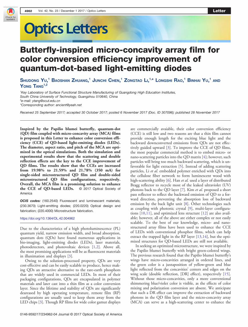
Butterfly-inspired micro-concavity array film forcolor conversion efficiency improvement ofquantum-dot-based light-emitting diodesSHUDONG YU,1 BAOSHAN ZHUANG,1 JUNCHI CHEN,1 ZONGTAO LI,1,* LONGSHI RAO,1 BINHAI YU,1 AND
YONG TANG1,2
1Key Laboratory of Surface Functional Structure Manufacturing of Guangdong High Education Institutes,South China University of Technology, Guangzhou 510640, China2e-mail: [email protected]*Corresponding author: [email protected]
Received 25 September 2017; accepted 30 October 2017; posted 6 November 2017 (Doc. ID 307096); published 28 November 2017
Inspired by the Papilio blumei butterfly, quantum-dot(QD) film coupled with micro-concavity array (MCA) filmsis proposed in this Letter to enhance color conversion effi-ciency (CCE) of QD-based light-emitting diodes (LEDs).The diameter, aspect ratio, and pitch of the MCA are opti-mized in the optical simulations. Both the simulation andexperimental results show that the scattering and doublereflection effects are the key to the CCE improvement ofQD films. The results show that the CCEs are increasedfrom 19.98% to 21.59% and 21.78% (350 mA) forsingle-sided microstructured QD film and double-sidedmicrostructured QD film configurations, respectively.Overall, the MCA film is a promising solution to enhancethe CCE of QD-based LEDs. © 2017 Optical Society ofAmerica
OCIS codes: (160.2540) Fluorescent and luminescent materials;
(230.3670) Light-emitting diodes; (220.0220) Optical design and
fabrication; (220.4000) Microstructure fabrication.
https://doi.org/10.1364/OL.42.004962
Due to the characteristics of a high photoluminescence (PL)quantum yield, narrow emission width, and broad absorption,quantum dots (QDs) have found numerous applications inbio-imaging, light-emitting diodes (LEDs), laser materials,photodetectors, and photovoltaic devices [1,2]. Above all,the most promising applications will be as fluorescent materialsin illunimation and displays [3].
Owing to the solution-processed property, QDs are verycost-effective and can be easily scalable to produce, hence mak-ing QDs an attractive alternative to the rare-earth phosphorsthat are widely used in commercial LEDs. In most of theirpackaging configurations, QDs are encapsulated in polymermaterials and later cast into a thin film as a color conversionlayer. Since the lifetime and stability of QDs are significantlydeareased by high operating temperature, remote film (RP)configurations are usually used to keep them away from theLED chips [3]. Though RP films for wide color gamut displays
are commercially avaiable, their color conversion efficiency(CCE) is still low and two reasons are that a thin film cannotprovide enough length for the exciting blue light and thebackward downconverted emissions from QDs are not effec-tively guided upward [3]. To improve the CCE of QD films,the most popular commercial method is to embed micro- ornano-scattering particles into the QDmatrix [4]; however, suchparticles will bring too much backward scattering, which is un-favorable for light extraction [5]. Instead of adding scatteringparticles, Li et al. embedded polymer enriched with QDs intothe cellulose fiber network to form luminescent wood withhigh-scattering ability [6]. Han et al. used a layer of distributedBragg reflector to recycle most of the leaked ultraviolet (UV)photons back to the QD layer [7]. Kim et al. proposed a shortpass reflector to reflect the backward emission of QD to a for-ward direction, preventing the absorption loss of backwardemission by the back light unit [8]. Other technologies suchas coupling with photonic crystal [9], multi-layer configura-tions [10,11], and optimized lens structure [12] are also avail-able; however, all of the above are either complex or not easilyscalable. To the best of our knowledge, micro- and nano-structured array films have been used to enhance the CCEof LEDs with conventional phosphor films, which can helpextract the trapped light in the RP layer [13,14], but the opti-mized structures for QD-based LEDs are still not available.
In seeking an optimized microstructure, we were inspired bythe Papilio blumei butterfly with bright green-colored wings.The previous research found that the Papilio blumei butterfly’swings have micro-concavities arranged in ordered lines, andthe green color is a juxtaposition of yellow-green and bluelight reflected from the concavities’ centers and edges on thewing scale (double reflection, [DR] effect), respectively [15].Without those micro-concavities, only a more conventionalshimmering blue/violet color is visible, as the effects of colormixing and polarization conversion are absent. We anticipatethat such a DR effect can improve the extraction of backwardphotons in the QD film layer and the micro-concavity array(MCA) can serve as a high-scattering center to enhance the
4962 Vol. 42, No. 23 / December 1 2017 / Optics Letters Letter
0146-9592/17/234962-04 Journal © 2017 Optical Society of America
optical length of the blue light in the QD layer. In this Letter,we optimize the parameters of MCA and fabricated QD filmsintegrated with MCA on both surfaces and demonstrate thatthe CCE of QD film configurations can be improved.
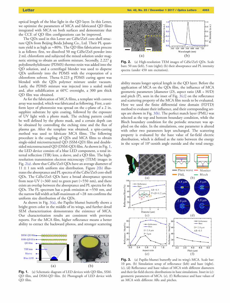
The QDs used in this Letter are CdSe/ZnS core-shell struc-ture QDs from Beijing Beida Jubang Co., Ltd. Their PL quan-tum yield is as high as ∼80%. The QD film fabrication processis as follows: first, we dissolved 50 mg CdSe/ZnS powder into2 mL chloroform and subjected the mixed solution under mag-netic stirring to obtain an uniform mixture. Secondly, 2.227 gpolydimethylsiloxane (PDMS) thermo-resin was added into theQD solution, and a centrifugal blender was used to disperseQDs uniformly into the PDMS with the evaporation of achloroform solvent. Thena 0.223 g PDMS curing agent wasblended with the QDs polymer mixture under vacuum.Lastly, the PDMS mixture was injected into a sealed moldand, after solidification at 60°C overnight, a 300 μm thickQD film was obtained.
As for the fabrication of MCA films, a template with convexarray was needed, which was fabricated as following. First, a uni-form layer of photoresist was spread on the c-plane of a 2 in.sapphire substrate by spin coating, followed by the exposureof UV light with a photo mask. The etching pattern couldbe well defined by the photo mask, and a certain depth canbe obtained by controlling the etching time and the flux ofplasma gas. After the template was obtained, a spin-castingmethod was used to fabricate MCA films. The followingprocedure is the coupling of QDs and MCA films to obtainsingle-sided microstructured QD (SSM-QD) film and double-sidedmicrostructuredQD (DSM-QD) film. As shown in Fig. 1,the LED device consists of a blue LED component, a total in-ternal reflection (TIR) lens, a sleeve, and a QD film. The high-resolution transmission electron microscopy (TEM) images inFig. 2(a). show that CdSe/ZnSQDs have an average diameter of11� 1 nm with uniform size distribution. Figure 2(b) illus-trates the absorptance and PL spectra of the CdSe/ZnS core-shellQDs. The CdSe/ZnS QDs have a broad absorptance spectrafrom near-UV (∼360 nm) to green part (∼550 nm), and thereexists an overlap between the absorptance and PL spectra for theQDs. The PL spectrum has a peak emission at ∼550 nm, andthe narrow full width at half-maximum of∼28 nm confirms theuniform size distribution of the QDs.
As shown in Fig. 3(a), the Papilio blumei butterfly shows abright green color in the middle of its wings, and further detailSEM characterization demonstrates the existence of MCA.Our characterization results are consistent with previousreports. For the MCA film, higher reflectance means a betterability to extract the backward photos, and stronger scattering
ability means longer optical length in the QD layer. Before theapplication of MCA on the QDs film, the influence of MCAgeometric parameters [diameter (D), aspect ratio (AR = H/D)and pitch (P), seen in the inset of Fig. 3(c)] on the reflectanceand scattering property of the MCA film needs to be evaluated.Here we used the finite differential time domain (FDTD)method to evaluate their influence, and their corresponding set-ups are shown in Fig. 3(b). The perfect match layer (PML) wasselected as the top and bottom boundary condition, while theBloch boundary condition for the periodic structure was ap-plied on the sides. In the simulations, one parameter is alteredwith other two parameters kept unchanged. The scatteringproperty is evaluated by the haze value of far-field electricdistribution, which is defined as the ratio between the energyin the scope of 10°-zenith angle outside and the total energy.
Fig. 1. (a) Schematic diagram of LED devices with QD film, SSM-QD film, and DSM-QD film. (b) Photograph of LED device withQD film.
Fig. 2. (a) High-resolution TEM images of CdSe/ZnS QDs. Scalebars: 50 nm (left), 5 nm (right); (b) their absorptance and PL intensityspectra (under 450 nm excitation).
Fig. 3. (a) Papilio blumei butterfly and its wing’s MCA. Scale bar:10 μm. (b) Simulation setup of reflectance (left) and haze (right).(c), (d) Reflectance and haze values of MCA with different diametersand their far-field electric distributions in haze simulations. Inset in (c):geometric parameters of MCA. (e), (f ) Reflectance and haze values ofan MCA with different ARs and pitches.
Letter Vol. 42, No. 23 / December 1 2017 / Optics Letters 4963
The simulation results are shown in Figs. 3(c)–3(f ).Considering the scattering ability and fabricating availability,we chose the diameter values below 5 μm as the parameters.As shown in Fig. 3(c), the reflectance and haze values increasewhen the diameter increases. However, the scattering uniform-ity is lowered when the diameter increases, shown in Fig. 3(d).The MCA with diameter of ∼5 μm refracts the incident light,not scattering the light, which is the main cause of its high hazevalue. Therefore, we chose 2.8 μm as the diameter to balancethe reflectance and scattering ability of the MCA. In the sim-ulations of MCA depth, different depth means different AR.The reflectance and haze values show better performance inthe AR range of 0.5–1, shown in Fig. 3(e). Since the MCAwith a high AR is difficult to fabricate, we chose 0.5 as theAR for further pitch optimization. As shown in Fig. 3(f ), boththe reflectance and haze values decrease with the increasingpitch; therefore, we set 3 μm as the MCA pitch.
To mimic such an MCA, a sapphire template with the op-timized MCA parameters D � 2.8 μm, AR � 0.5, and P �3 μm was used to obtain a biomimetic MCA film. As shownin Fig. 4(a), the MCA film shows a vivid iridescent color underdaylight due to the diffraction and interference effect of theMCA. In contrast, the prepared QD film with planar surfaceslacks diffraction fringe. As shown in Fig. 4(b), the DSM-QDfilm is well prepared. Through scanning electron microscope(SEM) characterization, we found that a range of hexagonallypacked MCA (diameter, ∼2.8 μm; depth, ∼1.3 μm; pitch,∼3 μm) is covered on the microstructured film, shown inFigs. 4(c) and 4(d). Since the dimension scale of the MCAis close to visible light wavelength (380–780 nm), it has astrong scattering and diffraction ability, which is responsiblefor the observed diffraction fringe on the MCA film.
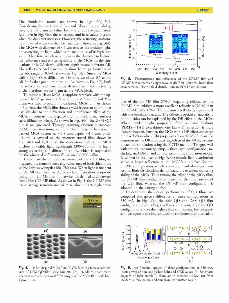
To evaluate the optical characteristic of the MCA film, wemeasured the transmittance and reflectance of both sides in thevisible light wavelength (380–780 nm). When light is incidenton the MCA surface, we define such configuration as upwardfacing film (UF-MP film); otherwise it is defined as downwardfacing film (DF-MP film). As shown in Fig. 5, the UF-MP filmhas an average transmittance of 95%, which is 20% higher than
that of the DF-MP film (75%). Regarding reflectance, theDF-MP film exhibits a more excellent reflectivity (21%) thanthe UF-MP film (5%). The measured reflectivity agrees wellwith the simulation results. The different optical characteristicof both sides can be explained by the DR effect of the MCA.When incident light propagates from a dense medium(PDMS ≈ 1.41) to a thinner one (air ≈ 1), reflection is morelikely to happen. Further, the MCA with a DR effect can causemore reflection when light propagates from the MCA to air. Todemonstrate the DR and scattering effects of the MCA, we con-ducted the simulation using the FDTD method. To agree wellwith the real measuring setup, a three-layer configuration, in-cluding air, PDMS, and air, was used in the simulation model.As shown in the inset of Fig. 5, the electric field distributionshows a larger reflection at the MCA/air interface for theDF-MP configuration, which is consistent with the experimentresults. Both distributions demonstrate the excellent scatteringability of the MCA. To maximize the effect of the MCA film,the UF-MP film configuration is used on the input surface ofthe QD film, whereas the DF-MP film configuration isadopted on the exiting surface.
To determine the optical performance of QD films, wecompared the spectra difference of three configurations at350 mA. In Fig. 6(a), the SSM-QD and DSM-QD filmconfigurations have a larger yellow component, while the QDconfiguration shows the highest blue component. For compari-son, we separate the blue and yellow components and calculate
Fig. 4. (a) Bio-inspiredMCA film. (b)QD film. Inset: cross-sectionalview of DSM-QD film; scale bar: 200 μm. (c), (d) Microstructuresside view and cross-sectional SEM images of the MCA film; scale bars:4 μm, 3 μm.
Fig. 5. Transmittance and reflectance of the UF-MP film andDF-MP film in the visible light wavelength (380–780 nm). Inset: theircross-sectional electric field distributions in FDTD simulations.
Fig. 6. (a) Emission spectra of three configurations at 350 mA.Inset: power of blue and yellow light and CCE values. (b) Schematicdiagram of light travel: (i) from air to incident surface, (ii) fromincident surface to air, and (iii) from exit surface to air.
4964 Vol. 42, No. 23 / December 1 2017 / Optics Letters Letter
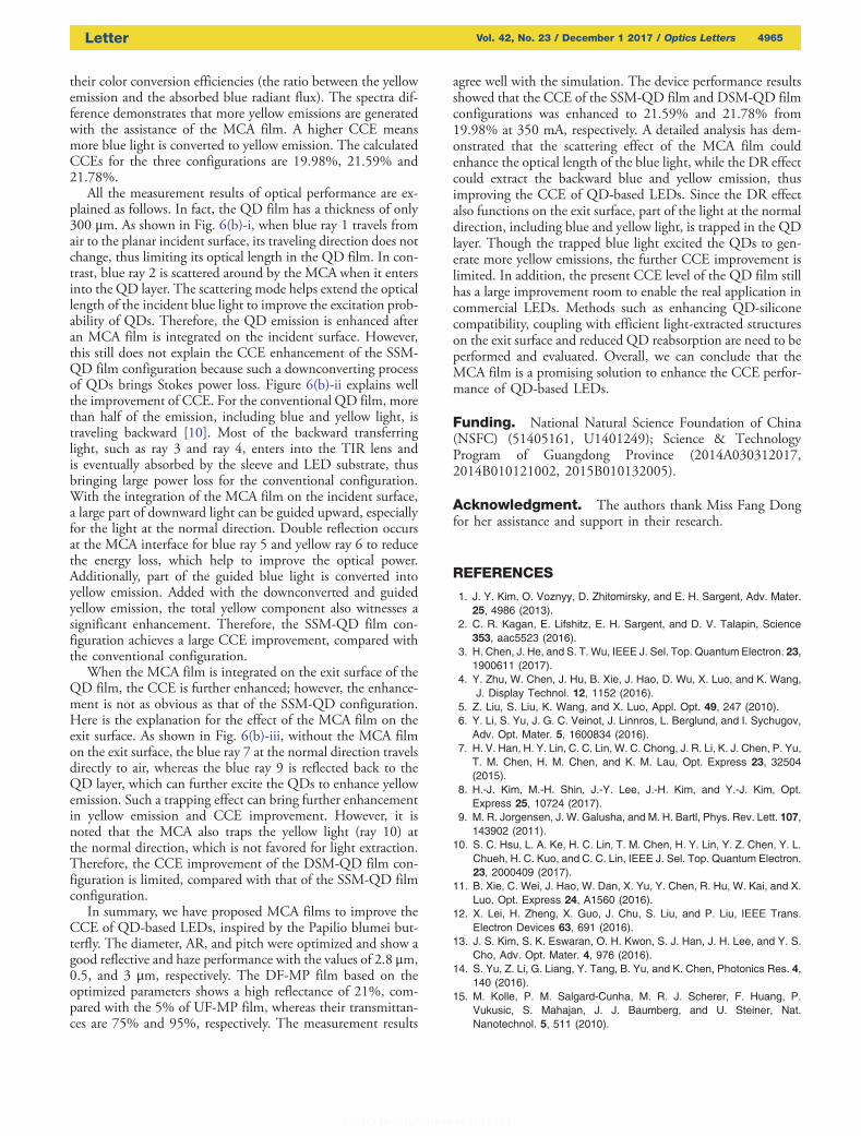
their color conversion efficiencies (the ratio between the yellowemission and the absorbed blue radiant flux). The spectra dif-ference demonstrates that more yellow emissions are generatedwith the assistance of the MCA film. A higher CCE meansmore blue light is converted to yellow emission. The calculatedCCEs for the three configurations are 19.98%, 21.59% and21.78%.
All the measurement results of optical performance are ex-plained as follows. In fact, the QD film has a thickness of only300 μm. As shown in Fig. 6(b)-i, when blue ray 1 travels fromair to the planar incident surface, its traveling direction does notchange, thus limiting its optical length in the QD film. In con-trast, blue ray 2 is scattered around by the MCA when it entersinto the QD layer. The scattering mode helps extend the opticallength of the incident blue light to improve the excitation prob-ability of QDs. Therefore, the QD emission is enhanced afteran MCA film is integrated on the incident surface. However,this still does not explain the CCE enhancement of the SSM-QD film configuration because such a downconverting processof QDs brings Stokes power loss. Figure 6(b)-ii explains wellthe improvement of CCE. For the conventional QD film, morethan half of the emission, including blue and yellow light, istraveling backward [10]. Most of the backward transferringlight, such as ray 3 and ray 4, enters into the TIR lens andis eventually absorbed by the sleeve and LED substrate, thusbringing large power loss for the conventional configuration.With the integration of the MCA film on the incident surface,a large part of downward light can be guided upward, especiallyfor the light at the normal direction. Double reflection occursat the MCA interface for blue ray 5 and yellow ray 6 to reducethe energy loss, which help to improve the optical power.Additionally, part of the guided blue light is converted intoyellow emission. Added with the downconverted and guidedyellow emission, the total yellow component also witnesses asignificant enhancement. Therefore, the SSM-QD film con-figuration achieves a large CCE improvement, compared withthe conventional configuration.
When the MCA film is integrated on the exit surface of theQD film, the CCE is further enhanced; however, the enhance-ment is not as obvious as that of the SSM-QD configuration.Here is the explanation for the effect of the MCA film on theexit surface. As shown in Fig. 6(b)-iii, without the MCA filmon the exit surface, the blue ray 7 at the normal direction travelsdirectly to air, whereas the blue ray 9 is reflected back to theQD layer, which can further excite the QDs to enhance yellowemission. Such a trapping effect can bring further enhancementin yellow emission and CCE improvement. However, it isnoted that the MCA also traps the yellow light (ray 10) atthe normal direction, which is not favored for light extraction.Therefore, the CCE improvement of the DSM-QD film con-figuration is limited, compared with that of the SSM-QD filmconfiguration.
In summary, we have proposed MCA films to improve theCCE of QD-based LEDs, inspired by the Papilio blumei but-terfly. The diameter, AR, and pitch were optimized and show agood reflective and haze performance with the values of 2.8 μm,0.5, and 3 μm, respectively. The DF-MP film based on theoptimized parameters shows a high reflectance of 21%, com-pared with the 5% of UF-MP film, whereas their transmittan-ces are 75% and 95%, respectively. The measurement results
agree well with the simulation. The device performance resultsshowed that the CCE of the SSM-QD film and DSM-QD filmconfigurations was enhanced to 21.59% and 21.78% from19.98% at 350 mA, respectively. A detailed analysis has dem-onstrated that the scattering effect of the MCA film couldenhance the optical length of the blue light, while the DR effectcould extract the backward blue and yellow emission, thusimproving the CCE of QD-based LEDs. Since the DR effectalso functions on the exit surface, part of the light at the normaldirection, including blue and yellow light, is trapped in the QDlayer. Though the trapped blue light excited the QDs to gen-erate more yellow emissions, the further CCE improvement islimited. In addition, the present CCE level of the QD film stillhas a large improvement room to enable the real application incommercial LEDs. Methods such as enhancing QD-siliconecompatibility, coupling with efficient light-extracted structureson the exit surface and reduced QD reabsorption are need to beperformed and evaluated. Overall, we can conclude that theMCA film is a promising solution to enhance the CCE perfor-mance of QD-based LEDs.
Funding. National Natural Science Foundation of China(NSFC) (51405161, U1401249); Science & TechnologyProgram of Guangdong Province (2014A030312017,2014B010121002, 2015B010132005).
Acknowledgment. The authors thank Miss Fang Dongfor her assistance and support in their research.
REFERENCES
1. J. Y. Kim, O. Voznyy, D. Zhitomirsky, and E. H. Sargent, Adv. Mater.25, 4986 (2013).
2. C. R. Kagan, E. Lifshitz, E. H. Sargent, and D. V. Talapin, Science353, aac5523 (2016).
3. H. Chen, J. He, and S. T. Wu, IEEE J. Sel. Top. Quantum Electron. 23,1900611 (2017).
4. Y. Zhu, W. Chen, J. Hu, B. Xie, J. Hao, D. Wu, X. Luo, and K. Wang,J. Display Technol. 12, 1152 (2016).
5. Z. Liu, S. Liu, K. Wang, and X. Luo, Appl. Opt. 49, 247 (2010).6. Y. Li, S. Yu, J. G. C. Veinot, J. Linnros, L. Berglund, and I. Sychugov,
Adv. Opt. Mater. 5, 1600834 (2016).7. H. V. Han, H. Y. Lin, C. C. Lin, W. C. Chong, J. R. Li, K. J. Chen, P. Yu,
T. M. Chen, H. M. Chen, and K. M. Lau, Opt. Express 23, 32504(2015).
8. H.-J. Kim, M.-H. Shin, J.-Y. Lee, J.-H. Kim, and Y.-J. Kim, Opt.Express 25, 10724 (2017).
9. M. R. Jorgensen, J. W. Galusha, and M. H. Bartl, Phys. Rev. Lett. 107,143902 (2011).
10. S. C. Hsu, L. A. Ke, H. C. Lin, T. M. Chen, H. Y. Lin, Y. Z. Chen, Y. L.Chueh, H. C. Kuo, and C. C. Lin, IEEE J. Sel. Top. Quantum Electron.23, 2000409 (2017).
11. B. Xie, C. Wei, J. Hao, W. Dan, X. Yu, Y. Chen, R. Hu, W. Kai, and X.Luo, Opt. Express 24, A1560 (2016).
12. X. Lei, H. Zheng, X. Guo, J. Chu, S. Liu, and P. Liu, IEEE Trans.Electron Devices 63, 691 (2016).
13. J. S. Kim, S. K. Eswaran, O. H. Kwon, S. J. Han, J. H. Lee, and Y. S.Cho, Adv. Opt. Mater. 4, 976 (2016).
14. S. Yu, Z. Li, G. Liang, Y. Tang, B. Yu, and K. Chen, Photonics Res. 4,140 (2016).
15. M. Kolle, P. M. Salgard-Cunha, M. R. J. Scherer, F. Huang, P.Vukusic, S. Mahajan, J. J. Baumberg, and U. Steiner, Nat.Nanotechnol. 5, 511 (2010).
Letter Vol. 42, No. 23 / December 1 2017 / Optics Letters 4965