Embed Size (px)
Citation preview
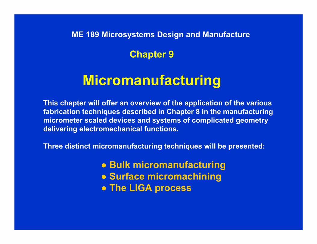
ME 189 Microsystems Design and Manufacture
Chapter 9
MicromanufacturingThis chapter will offer an overview of the application of the various fabrication techniques described in Chapter 8 in the manufacturing micrometer scaled devices and systems of complicated geometrydelivering electromechanical functions.
Three distinct micromanufacturing techniques will be presented:
● Bulk micromanufacturing● Surface micromachining● The LIGA process
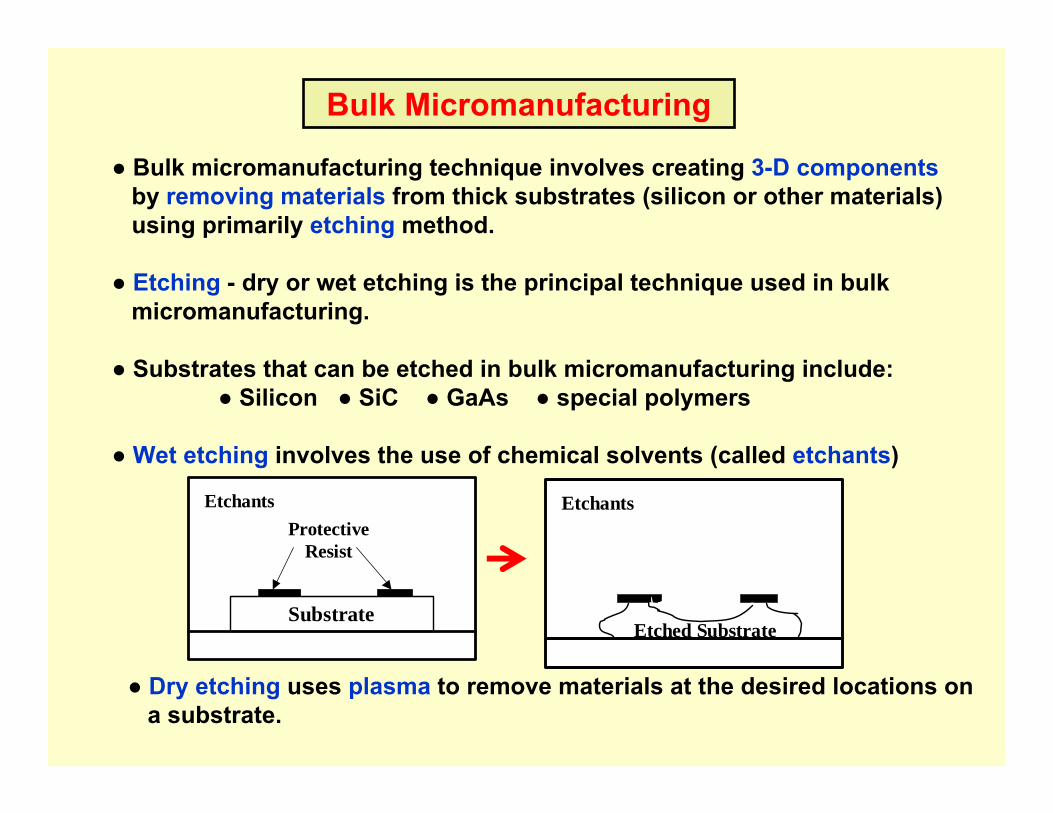
Bulk Micromanufacturing
● Bulk micromanufacturing technique involves creating 3-D componentsby removing materials from thick substrates (silicon or other materials)using primarily etching method.
● Etching - dry or wet etching is the principal technique used in bulkmicromanufacturing.
● Substrates that can be etched in bulk micromanufacturing include:● Silicon ● SiC ● GaAs ● special polymers
● Wet etching involves the use of chemical solvents (called etchants)
EtchantsProtective
Resist
Substrate
Etchants
Etched Substrate
● Dry etching uses plasma to remove materials at the desired locations ona substrate.
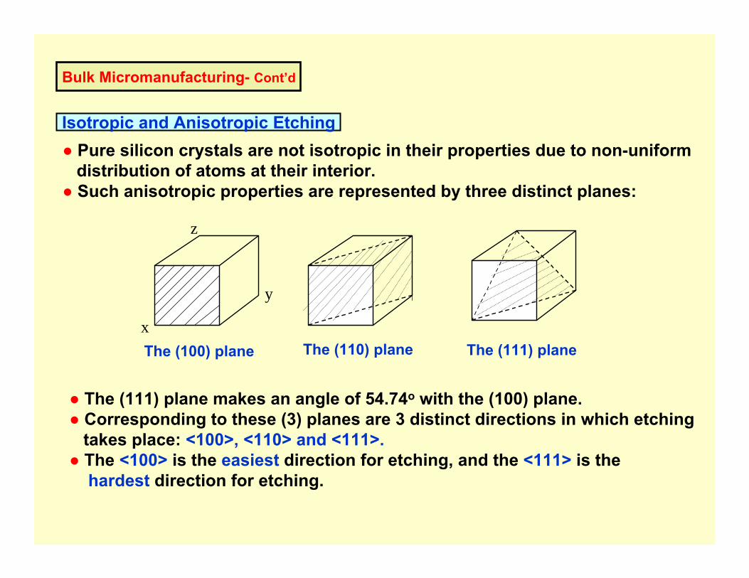
Bulk Micromanufacturing- Cont’d
Isotropic and Anisotropic Etching● Pure silicon crystals are not isotropic in their properties due to non-uniform
distribution of atoms at their interior.● Such anisotropic properties are represented by three distinct planes:
x
y
z
The (100) plane The (110) plane The (111) plane
● The (111) plane makes an angle of 54.74o with the (100) plane.● Corresponding to these (3) planes are 3 distinct directions in which etching
takes place: <100>, <110> and <111>.● The <100> is the easiest direction for etching, and the <111> is the
hardest direction for etching.
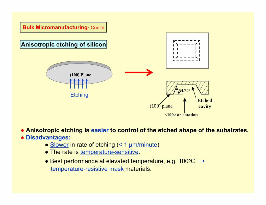
Bulk Micromanufacturing- Cont’d
Anisotropic etching of silicon
(100) Plane
54.74o
Etchedcavity(100) plane
<100> orientation
Etching
● Anisotropic etching is easier to control of the etched shape of the substrates. ● Disadvantages:
● Slower in rate of etching (< 1 µm/minute)● The rate is temperature-sensitive.● Best performance at elevated temperature, e.g. 100oC →
temperature-resistive mask materials.
Bulk Micromanufacturing- Cont’d
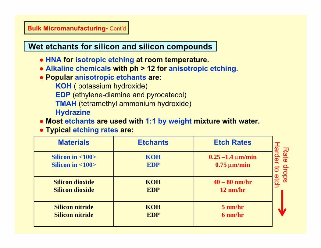
Wet etchants for silicon and silicon compounds● HNA for isotropic etching at room temperature.● Alkaline chemicals with ph > 12 for anisotropic etching.● Popular anisotropic etchants are:
KOH ( potassium hydroxide)EDP (ethylene-diamine and pyrocatecol)TMAH (tetramethyl ammonium hydroxide)Hydrazine
● Most etchants are used with 1:1 by weight mixture with water.● Typical etching rates are:
5 nm/hr6 nm/hr
KOHEDP
Silicon nitrideSilicon nitride
40 – 80 nm/hr12 nm/hr
KOHEDP
Silicon dioxideSilicon dioxide
0.25 –1.4 µm/min0.75 µm/min
KOHEDP
Silicon in <100>Silicon in <100>
Etch RatesEtchantsMaterials Rate drops
Harder to etch
Bulk Micromanufacturing- Cont’d
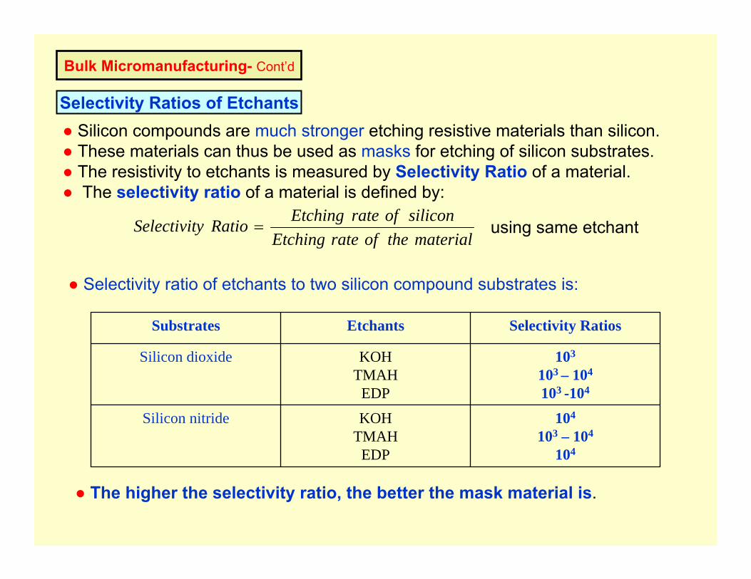
Selectivity Ratios of Etchants● Silicon compounds are much stronger etching resistive materials than silicon.● These materials can thus be used as masks for etching of silicon substrates.● The resistivity to etchants is measured by Selectivity Ratio of a material.● The selectivity ratio of a material is defined by:
materialtheofrateEtchingsiliconofrateEtchingRatioySelectivit =
● Selectivity ratio of etchants to two silicon compound substrates is:
104
103 – 104
104
KOHTMAH
EDP
Silicon nitride
103
103 – 104
103 -104
KOHTMAH
EDP
Silicon dioxide
Selectivity RatiosEtchantsSubstrates
● The higher the selectivity ratio, the better the mask material is.
using same etchant
Bulk Micromanufacturing- Cont’d
Control of wet etching
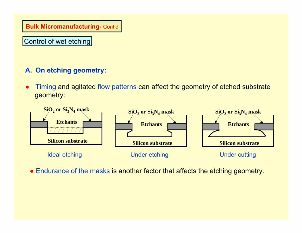
A. On etching geometry:
● Timing and agitated flow patterns can affect the geometry of etched substrategeometry:
Etchants
SiO2 or Si3N4 mask
Silicon substrate
Etchants
SiO2 or Si3N4 mask
Silicon substrate
Etchants
SiO2 or Si3N4 mask
Silicon substrate
Ideal etching Under etching Under cutting
● Endurance of the masks is another factor that affects the etching geometry.
Bulk Micromanufacturing- Cont’d
Control of wet etching – Cont’d
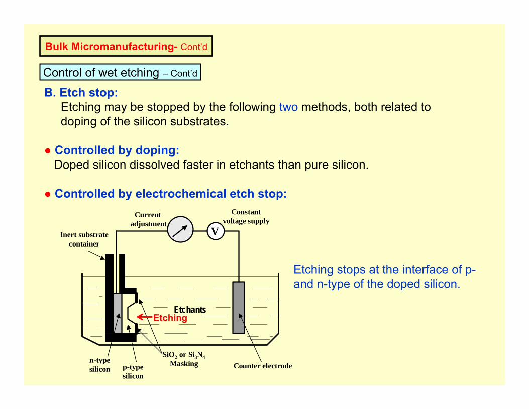
B. Etch stop:Etching may be stopped by the following two methods, both related to doping of the silicon substrates.
● Controlled by doping:Doped silicon dissolved faster in etchants than pure silicon.
● Controlled by electrochemical etch stop:
V
Constantvoltage supply
Current adjustment
Inert substratecontainer
n-typesilicon p-type
silicon
SiO2 or Si3N4Masking
Etchants
Counter electrode
Etching stops at the interface of p-and n-type of the doped silicon.
Etching
Bulk Micromanufacturing- Cont’d
Dry EtchingDry etching involves the removal of substrate materials by gaseous etchants.It is more a physical than chemical process.
3 dry etching techniques:● Ion etching.● Plasma etching.● Reactive ion etching. Deep reactive ion etching (DRIE)
Plasma etching:
Plasma is a neutral ionized gas carrying a large number of free electrons and positively charged ions.
A common source of energy for generating plasma is the radio frequency (RF) source.
Chemical reactive gas, e.g. CCℓ2F2, is mixed with plasma in etching process.Other chemical reactive gases for different substrates are given in Table 9.3.
Bulk Micromanufacturing- Cont’d
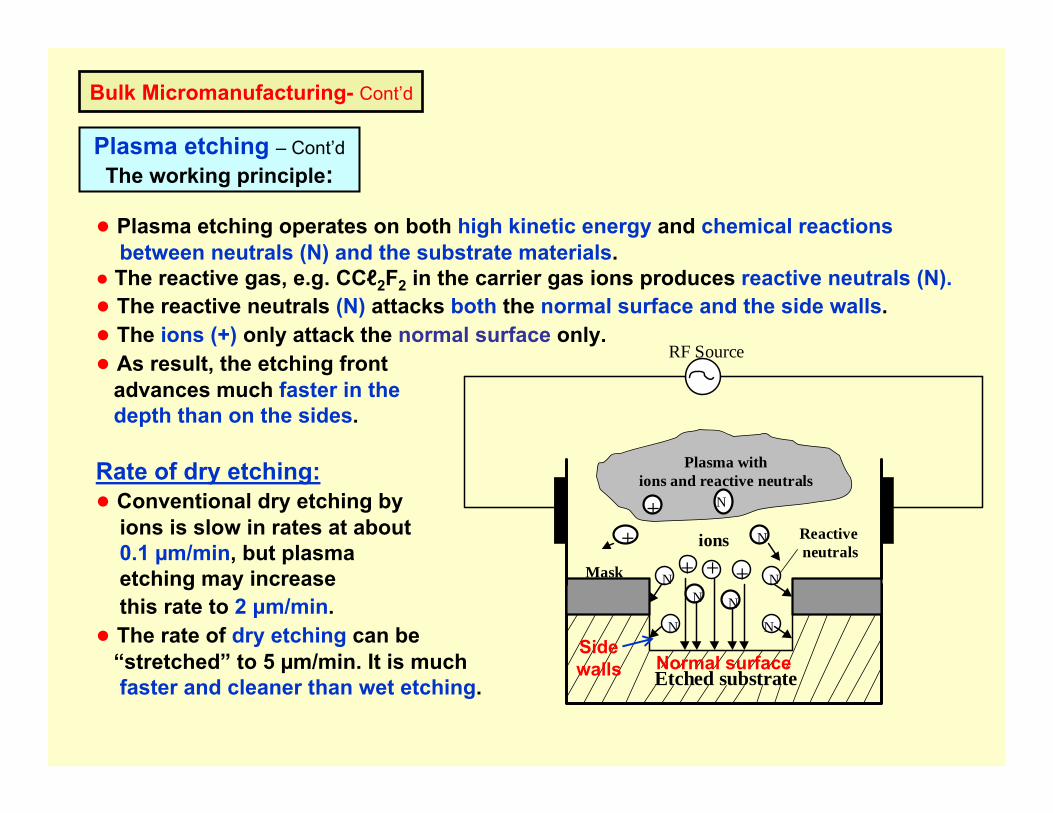
Plasma etching – Cont’dThe working principle:
+ + +N N
N N
ions Reactive neutrals
Plasma withions and reactive neutrals
Etched substrate
Mask
+ N
+ N
RF Source
N N
● Plasma etching operates on both high kinetic energy and chemical reactions between neutrals (N) and the substrate materials.
● The reactive gas, e.g. CCℓ2F2 in the carrier gas ions produces reactive neutrals (N).● The reactive neutrals (N) attacks both the normal surface and the side walls.● The ions (+) only attack the normal surface only.● As result, the etching front
advances much faster in the depth than on the sides.
Rate of dry etching:● Conventional dry etching by
ions is slow in rates at about 0.1 µm/min, but plasma etching may increase this rate to 2 µm/min.
● The rate of dry etching can be“stretched” to 5 µm/min. It is muchfaster and cleaner than wet etching.
Normal surfaceSidewalls
Bulk Micromanufacturing- Cont’d
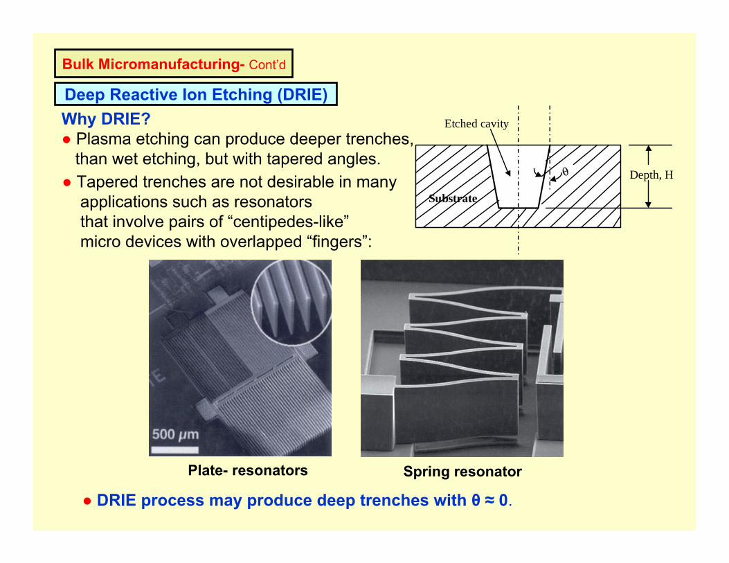
Deep Reactive Ion Etching (DRIE)Why DRIE?● Plasma etching can produce deeper trenches,
than wet etching, but with tapered angles.● Tapered trenches are not desirable in many
applications such as resonators that involve pairs of “centipedes-like”micro devices with overlapped “fingers”:
θ
Etched cavity
Substrate
Depth, H
● DRIE process may produce deep trenches with θ ≈ 0.
Plate- resonators Spring resonator
Bulk Micromanufacturing- Cont’d
Deep Reactive Ion Etching (DRIE)
+ + +N N
N N
ions Reactive neutrals
Plasma withions and reactive neutrals
DRIE etched substrate
Mask
+ N
+ N
NN
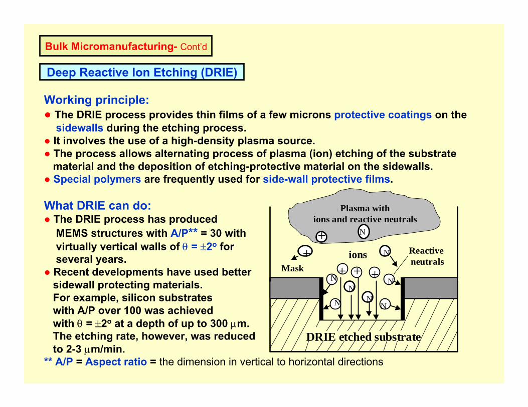
Working principle:● The DRIE process provides thin films of a few microns protective coatings on the
sidewalls during the etching process. ● It involves the use of a high-density plasma source.● The process allows alternating process of plasma (ion) etching of the substrate
material and the deposition of etching-protective material on the sidewalls. ● Special polymers are frequently used for side-wall protective films.
What DRIE can do:● The DRIE process has produced
MEMS structures with A/P** = 30 with virtually vertical walls of θ = ±2o for several years.
● Recent developments have used better sidewall protecting materials. For example, silicon substrates with A/P over 100 was achieved with θ = ±2o at a depth of up to 300 µm. The etching rate, however, was reduced to 2-3 µm/min.
** A/P = Aspect ratio = the dimension in vertical to horizontal directions
Bulk Micromanufacturing- cont’d
Deep Reactive Ion Etching (DRIE)- Cont’d
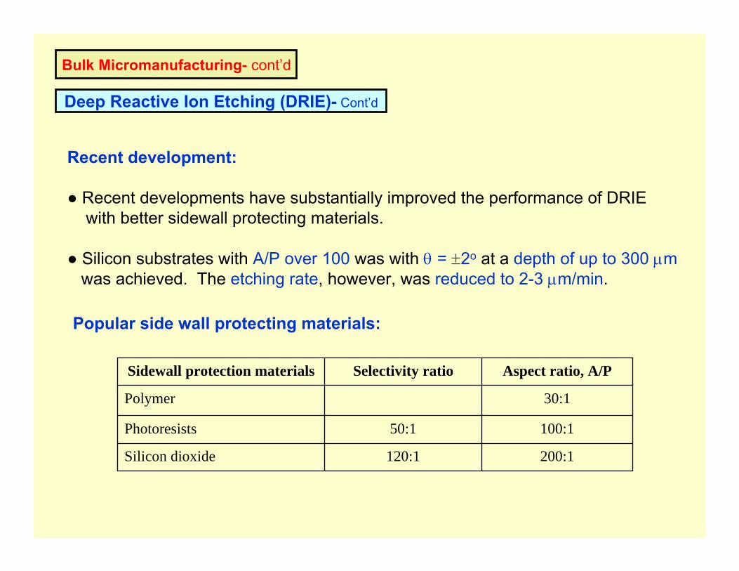
Recent development:
● Recent developments have substantially improved the performance of DRIE with better sidewall protecting materials.
● Silicon substrates with A/P over 100 was with θ = ±2o at a depth of up to 300 µmwas achieved. The etching rate, however, was reduced to 2-3 µm/min.
Popular side wall protecting materials:
200:1120:1Silicon dioxide
100:150:1Photoresists
30:1Polymer
Aspect ratio, A/PSelectivity ratioSidewall protection materials
Bulk Micromanufacturing- ends
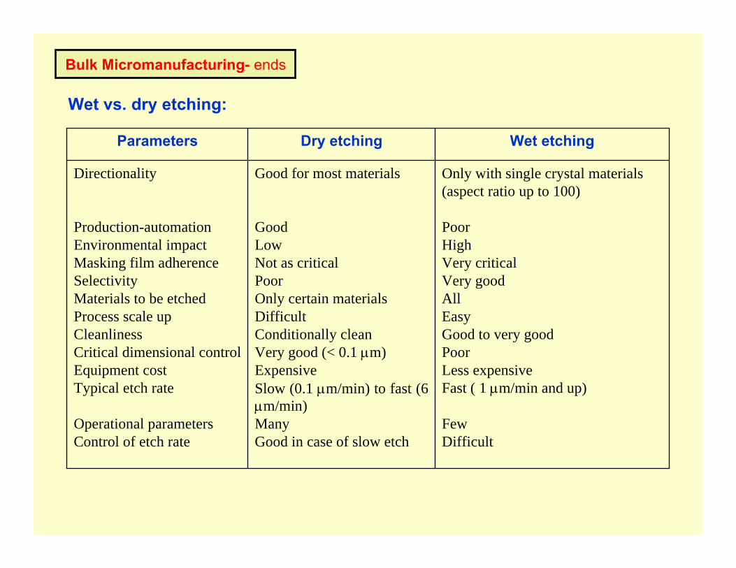
Wet vs. dry etching:
Only with single crystal materials (aspect ratio up to 100)
PoorHighVery criticalVery goodAllEasyGood to very goodPoorLess expensiveFast ( 1 µm/min and up)
FewDifficult
Good for most materials
GoodLowNot as criticalPoorOnly certain materialsDifficultConditionally cleanVery good (< 0.1 µm)ExpensiveSlow (0.1 µm/min) to fast (6 µm/min)ManyGood in case of slow etch
Directionality
Production-automationEnvironmental impactMasking film adherenceSelectivityMaterials to be etchedProcess scale upCleanlinessCritical dimensional controlEquipment costTypical etch rate
Operational parametersControl of etch rate
Wet etchingDry etchingParameters
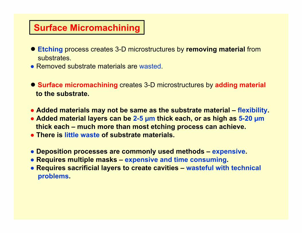
Surface Micromachining
● Etching process creates 3-D microstructures by removing material from substrates.
● Removed substrate materials are wasted.
● Surface micromachining creates 3-D microstructures by adding material to the substrate.
● Added materials may not be same as the substrate material – flexibility.● Added material layers can be 2-5 µm thick each, or as high as 5-20 µm
thick each – much more than most etching process can achieve.● There is little waste of substrate materials.
● Deposition processes are commonly used methods – expensive.● Requires multiple masks – expensive and time consuming.● Requires sacrificial layers to create cavities – wasteful with technical
problems.
Surface Micromachining – Cont’d
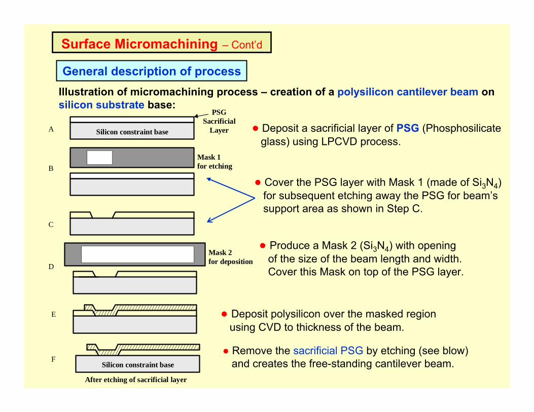
Illustration of micromachining process – creation of a polysilicon cantilever beam on silicon substrate base:
A
Silicon constraint base
B
C
D
E
F
Silicon constraint base
Mask 1for etching
Mask 2for deposition
PSGSacrificial
Layer
After etching of sacrificial layer
● Deposit a sacrificial layer of PSG (Phosphosilicateglass) using LPCVD process.
● Cover the PSG layer with Mask 1 (made of Si3N4)for subsequent etching away the PSG for beam’s support area as shown in Step C.
● Produce a Mask 2 (Si3N4) with openingof the size of the beam length and width.Cover this Mask on top of the PSG layer.
● Deposit polysilicon over the masked regionusing CVD to thickness of the beam.
● Remove the sacrificial PSG by etching (see blow)and creates the free-standing cantilever beam.
General description of process
Surface Micromachining – Cont’d
General description of process- Cont’d
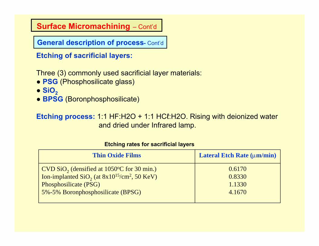
Etching of sacrificial layers:
Three (3) commonly used sacrificial layer materials:● PSG (Phosphosilicate glass)● SiO2● BPSG (Boronphosphosilicate)
Etching process: 1:1 HF:H2O + 1:1 HCℓ:H2O. Rising with deionized water and dried under Infrared lamp.
0.61700.83301.13304.1670
CVD SiO2 (densified at 1050oC for 30 min.)Ion-implanted SiO2 (at 8x10¹⁵/cm2, 50 KeV)Phosphosilicate (PSG)5%-5% Boronphosphosilicate (BPSG)
Lateral Etch Rate (µm/min)Thin Oxide Films
Etching rates for sacrificial layers
Surface Micromachining – Cont’d
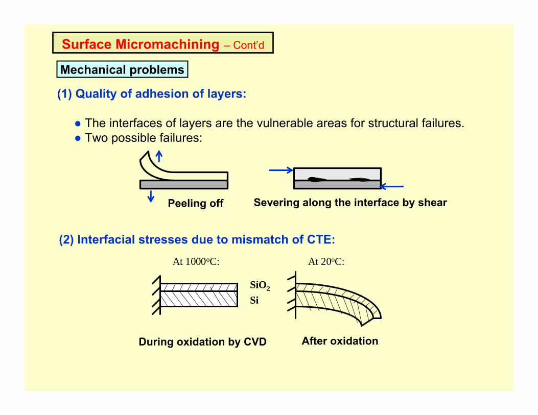
Mechanical problems
(1) Quality of adhesion of layers:
● The interfaces of layers are the vulnerable areas for structural failures.● Two possible failures:
Peeling off Severing along the interface by shear
(2) Interfacial stresses due to mismatch of CTE:
At 1000oC: At 20oC:
SiO2
Si
During oxidation by CVD After oxidation
Surface Micromachining – Ends
Mechanical problems – Cont’d
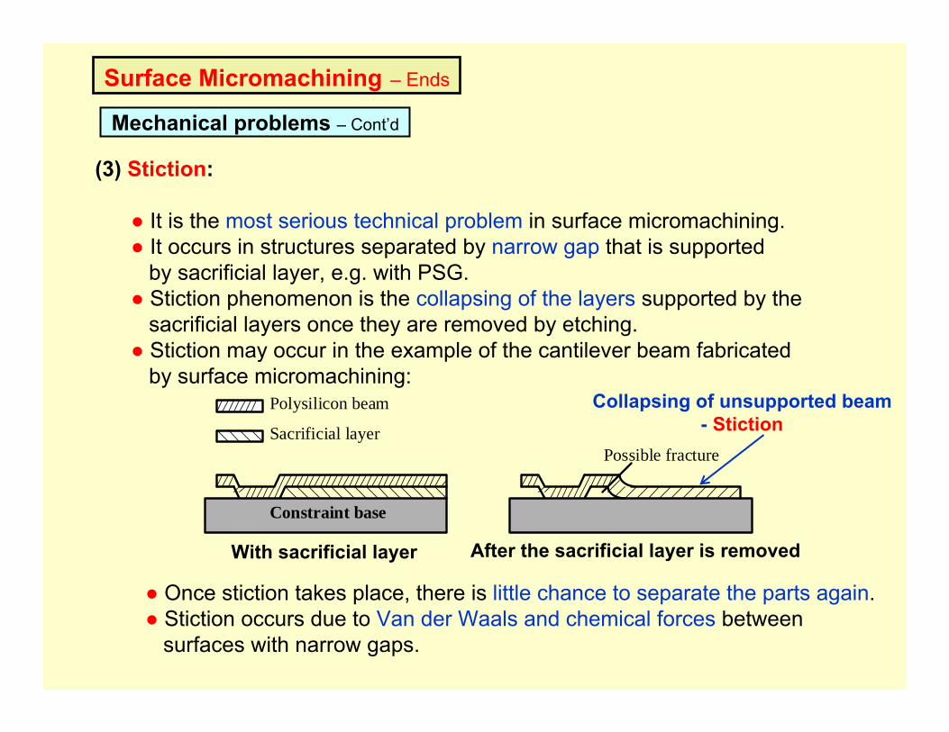
(3) Stiction:
● It is the most serious technical problem in surface micromachining.● It occurs in structures separated by narrow gap that is supported
by sacrificial layer, e.g. with PSG.● Stiction phenomenon is the collapsing of the layers supported by the
sacrificial layers once they are removed by etching.● Stiction may occur in the example of the cantilever beam fabricated
by surface micromachining:
Sacrificial layer
Polysilicon beam
Constraint base
Possible fracture
With sacrificial layer After the sacrificial layer is removed
● Once stiction takes place, there is little chance to separate the parts again.● Stiction occurs due to Van der Waals and chemical forces between
surfaces with narrow gaps.
Collapsing of unsupported beam- Stiction
The LIGA Process
● The term LIGA is an acronym for German term in “Lithography (Lithographie), electroforming (Galvanoformung), and molding (Abformung)”.
● The technique was first developed at the Karlsruhe Nuclear Research Center in Karlsruhe, Germany.
● LIGA process is radically different from silicon-based micro manufacturing.
● The major difference is that LIGA can produce microstructures that have high aspect ratio.
● There is no restriction on using silicon or silicon compounds as substrate.Nickel is a common material for LIGA products.
● It is easier to be produced in large volumes.
● Major disadvantage of LIGA process is the requirement of special facility- Synchrotron radiation (X-ray) source, a very expensive facility.
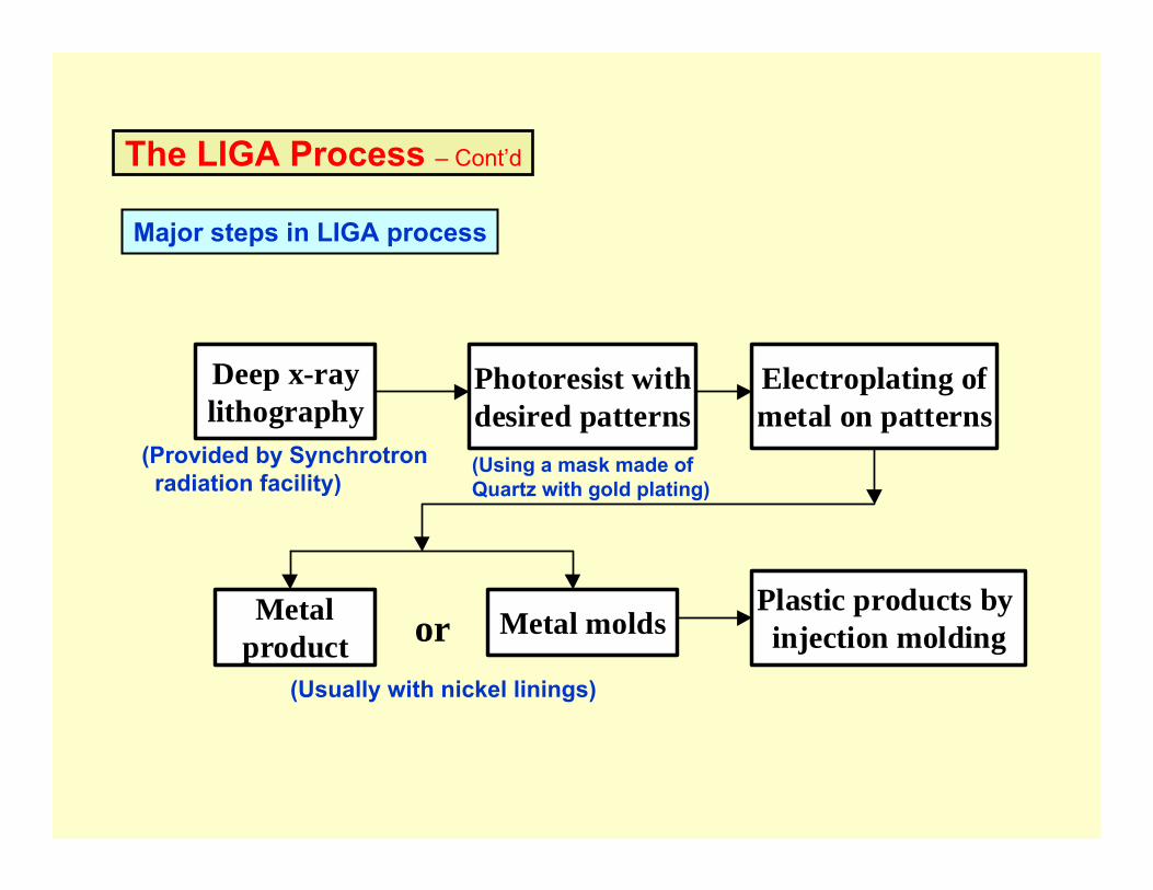
The LIGA Process – Cont’d
Major steps in LIGA process
Deep x-raylithography
Photoresist withdesired patterns
Electroplating ofmetal on patterns
Metalproduct
Metal moldsPlastic products by injection moldingor
(Provided by Synchrotronradiation facility)
(Using a mask made ofQuartz with gold plating)
(Usually with nickel linings)
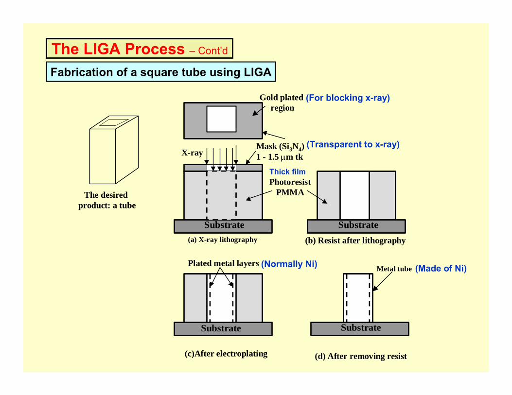
The LIGA Process – Cont’d
Fabrication of a square tube using LIGA
The desired product: a tube
Gold plated region
Mask (Si3N4)1 - 1.5 µm tkX-ray
PhotoresistPMMA
Substrate(a) X-ray lithography (b) Resist after lithography
(c)After electroplating (d) After removing resist
Substrate
Substrate
Substrate
Plated metal layersMetal tube
Thick film
(For blocking x-ray)
(Transparent to x-ray)
(Normally Ni) (Made of Ni)
The LIGA Process – Cont’d
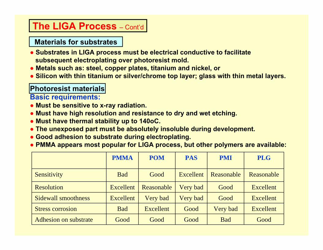
Materials for substrates● Substrates in LIGA process must be electrical conductive to facilitate
subsequent electroplating over photoresist mold.● Metals such as: steel, copper plates, titanium and nickel, or● Silicon with thin titanium or silver/chrome top layer; glass with thin metal layers.
Photoresist materialsBasic requirements:● Must be sensitive to x-ray radiation.● Must have high resolution and resistance to dry and wet etching.● Must have thermal stability up to 140oC.● The unexposed part must be absolutely insoluble during development.● Good adhesion to substrate during electroplating.● PMMA appears most popular for LIGA process, but other polymers are available:
GoodBadGoodGoodGoodAdhesion on substrate
ExcellentVery badGoodExcellentBadStress corrosion
ExcellentGoodVery badVery badExcellentSidewall smoothness
ExcellentGoodVery badReasonableExcellentResolution
ReasonableReasonableExcellentGoodBadSensitivity
PLGPMIPASPOMPMMA
The LIGA Process – Ends
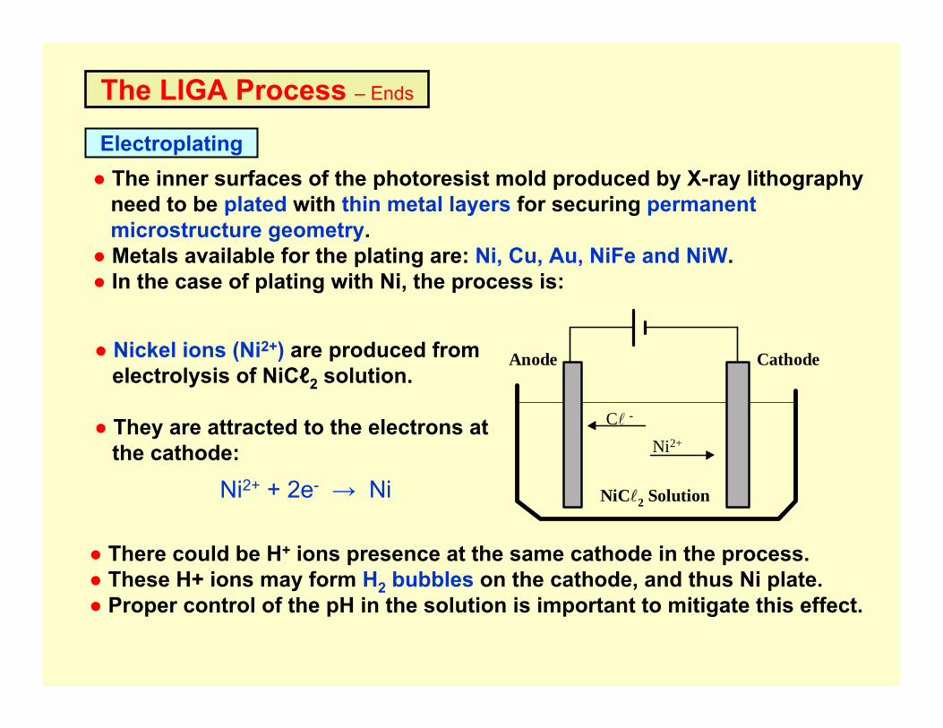
Electroplating● The inner surfaces of the photoresist mold produced by X-ray lithography
need to be plated with thin metal layers for securing permanent microstructure geometry.
● Metals available for the plating are: Ni, Cu, Au, NiFe and NiW.● In the case of plating with Ni, the process is:
Anode Cathode
NiCl2 Solution
Cl -
Ni2+
● There could be H+ ions presence at the same cathode in the process. ● These H+ ions may form H2 bubbles on the cathode, and thus Ni plate.● Proper control of the pH in the solution is important to mitigate this effect.
● Nickel ions (Ni2+) are produced from electrolysis of NiCℓ2 solution.
● They are attracted to the electrons at the cathode:
Ni2+ + 2e- → Ni
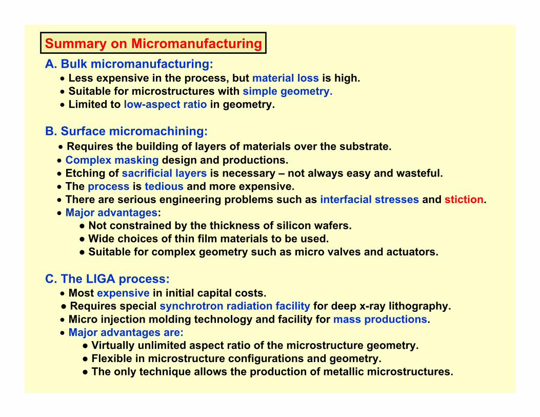
Summary on MicromanufacturingA. Bulk micromanufacturing:
• Less expensive in the process, but material loss is high.• Suitable for microstructures with simple geometry.• Limited to low-aspect ratio in geometry.
B. Surface micromachining:• Requires the building of layers of materials over the substrate.• Complex masking design and productions.• Etching of sacrificial layers is necessary – not always easy and wasteful.• The process is tedious and more expensive.• There are serious engineering problems such as interfacial stresses and stiction.• Major advantages:
● Not constrained by the thickness of silicon wafers.● Wide choices of thin film materials to be used.● Suitable for complex geometry such as micro valves and actuators.
C. The LIGA process:• Most expensive in initial capital costs.● Requires special synchrotron radiation facility for deep x-ray lithography.• Micro injection molding technology and facility for mass productions.• Major advantages are:
● Virtually unlimited aspect ratio of the microstructure geometry.● Flexible in microstructure configurations and geometry.● The only technique allows the production of metallic microstructures.