Embed Size (px)
Citation preview
Building Blocks for Sampling and Digitization inHigh-speed Communication Systems
by
Chunyang Zhai
A dissertation submitted in partial fulfillmentof the requirements for the degree of
Doctor of Philosophy(Electrical Engineering)
in The University of Michigan2017
Doctoral Committee:
Professor Michael P. Flynn, ChairProfessor Zhong HeAssociate Professor David D. WentzloffAssociate Professor Zhengya Zhang

c© Chunyang Zhai 2017
All Rights Reserved
ACKNOWLEDGEMENTS
Academic and research work are always boring and difficult. Fortunately, my
Ph.D journey at University of Michigan is enjoyable and rewarding, because I have
met so many great people. First and foremost, I would like to express my greatest
gratitude to my advisor, Professor Michael Flynn, for his continuous support and
guidance to my study and research. He is not only an advisor with great breadth
and depth of technical knowledge, but also a mentor for my future career and life.
Second, I would like to express my appreciation to Professor David Wentzloff,
Professor Zhengya Zhang and Professor Zhong He for serving as my dissertation
committee members and providing invaluable advice and encouragements. Particu-
larly, I want to thank Professor Zhengya Zhang for his help and guidance on my
future career development.
I would also thank all the great colleagues in Flynn research group. I feel
fortunate having them throughout my years at Michigan. They are: Aramis Alvarez,
John Bell, Peter Brown, Fred Buhler, Hyungil Chae, Kyojin Choo, Nick Collins,
Justin Correll, Batuhan Dayanik, Jeffrey Fredenburg, Mahammad Ghahramamani,
Sunmin Jang, Jaehun Jeong, Li Li, Yong Lim, David Lin, Rundao Lu, Steven
ii

Mikes, Jorge Pernillo, Hyo Gyuem Rhew, Daniel Weyer, Boyi Zheng. I really
appreciate the numerous technical discussions with them. We were always there to
help each other during tapeouts. I’ll miss the stay up late coffee and small talks.
I am thankful for the help from students in Wentzloff group, Elnaz Ansari,
Xing Chen, Hyeongseok Kim, Avish Kosari and Yao Shi on the discussions on
RF circuit design and testing. I wish to thank Professor Anthony Grbic and his
student Nikolaos Chiotellis on the discussions on on-chip transmission line design.
I would also like to thank Thomas Chen, Qing Dong, Kaiyuan Yang, Shiming
Song, Shuanghong Sun and Yiqun Zhang. When I was fighting with digital circuit
design tools, I could always ask them for help. Im also grateful to our wonderful
staffs, Fran Doman, for her always there to help me out and making sure everything
goes smoothly; Joel VanLaven, for his great help on simulator tools support and
software issues debugging.
Finally and most importantly, I am deeply indebted to my parents for their
unconditional love and endless support. They are the wind beneath my wings. I
cannot thank more to my dear sister for her love and caring ever since I was a
baby girl. I deeply appreciate that my sister and brother-in-law took good care of
my parents when I was in the United States to finish my Ph.D study. I would like
to thank my husband, who is also my best friend, Dr. Qi Zheng for his love and
support, more importantly, for his accompany in this lifelong journey.
Go Blue!
iii
TABLE OF CONTENTS
ACKNOWLEDGEMENTS . . . . . . . . . . . . . . . . . . . . . . . . ii
LIST OF FIGURES . . . . . . . . . . . . . . . . . . . . . . . . . . . vi
LIST OF ABBREVIATIONS . . . . . . . . . . . . . . . . . . . . . . viii
ABSTRACT . . . . . . . . . . . . . . . . . . . . . . . . . . . . . . . . x
CHAPTER
I. Introduction . . . . . . . . . . . . . . . . . . . . . . . . . . . . 1
1.1 High-speed Communication Systems . . . . . . . . . . . 11.1.1 The Growth of High-speed Communication
Systems . . . . . . . . . . . . . . . . . . . . . 11.1.2 Key Building Blocks in a High-speed Commu-
nication System . . . . . . . . . . . . . . . . . 41.2 Contributions . . . . . . . . . . . . . . . . . . . . . . . 81.3 Organization . . . . . . . . . . . . . . . . . . . . . . . . 10
II. Background . . . . . . . . . . . . . . . . . . . . . . . . . . . . 11
2.1 Oscillators in High-speed Communication Systems . . . 112.1.1 Voltage-controlled Oscillators . . . . . . . . . 122.1.2 Two Types of Voltage-controlled Oscillators . . 16
2.2 High Speed ADCs in High-speed Communication Systems 192.2.1 High Speed ADC Applications . . . . . . . . . 19
iv
2.2.2 High Speed ADC Techniques . . . . . . . . . 192.3 High Speed Sampling and Digitization . . . . . . . . . . 26
III. An N-path Filter Enhanced Low Phase Noise Ring VCO . . . 28
3.1 Ring Voltage-controlled Oscillator . . . . . . . . . . . . 283.2 N-path Filter . . . . . . . . . . . . . . . . . . . . . . . . 303.3 NPFRVCO Circuit Implementation . . . . . . . . . . . . 323.4 Measurements . . . . . . . . . . . . . . . . . . . . . . . 37
IV. Traveling-Wave ADC . . . . . . . . . . . . . . . . . . . . . . . 42
4.1 High Speed ADC with On-chip Transmission Line . . . . 424.2 System Architecture . . . . . . . . . . . . . . . . . . . . 444.3 System Implementation . . . . . . . . . . . . . . . . . . 47
4.3.1 On-chip Transmission Line . . . . . . . . . . . 474.3.2 High Speed Comparator . . . . . . . . . . . . 534.3.3 Current-steering DAC . . . . . . . . . . . . . 56
4.4 Measurements . . . . . . . . . . . . . . . . . . . . . . . 604.5 Test Setup . . . . . . . . . . . . . . . . . . . . . . . . . 64
V. Future Work . . . . . . . . . . . . . . . . . . . . . . . . . . . . 66
VI. Conclusion . . . . . . . . . . . . . . . . . . . . . . . . . . . . . 68
BIBLIOGRAPHY . . . . . . . . . . . . . . . . . . . . . . . . . . . . 70
v
LIST OF FIGURES
Figure
1.1 5G applications [1] . . . . . . . . . . . . . . . . . . . . . . . . 21.2 High speed links inside a router [2] . . . . . . . . . . . . . . . 31.3 Basic components in a communication system . . . . . . . . . 41.4 Superheterodyne receiver (a) and transitter (b) . . . . . . . . 51.5 High speed link system [3] . . . . . . . . . . . . . . . . . . . . 72.1 Resource block defination in frequency domain-LTE [4] . . . 122.2 PLL for wireless tranceiver . . . . . . . . . . . . . . . . . . . 132.3 The effect of timing jitter sampling error [5] . . . . . . . . . 152.4 Theoretical SNR and ENOB due to jitter vs. input frequency
for different values of the RMS jitter [6] . . . . . . . . . . . . 172.5 Typical LC oscillator structure . . . . . . . . . . . . . . . . . 172.6 Typical ring VCO structure . . . . . . . . . . . . . . . . . . . 182.7 Block diagram of a converntional flash ADC . . . . . . . . . 202.8 Block diagram of a converntional SAR ADC . . . . . . . . . 212.9 Block diagram of a pipeline ADC . . . . . . . . . . . . . . . . 222.10 Block diagram of a delta-sigma ADC . . . . . . . . . . . . . . 232.11 Walden FoM vs. sampling clock rate of ADCs . . . . . . . . . 263.1 Power spectrum of RVCO and desired power spectrum of
NPFRVCO . . . . . . . . . . . . . . . . . . . . . . . . . . . . 293.2 Low pass filter transformed to bandpass filter . . . . . . . . . 303.3 N-path band-pass filter network . . . . . . . . . . . . . . . . 303.4 Control signals for switches (a) and simplified N-path filter (b) 313.5 N-path filter equivalent structure . . . . . . . . . . . . . . . . 323.6 NPRVCO block diagram . . . . . . . . . . . . . . . . . . . . 333.7 NPFRVCO implementation . . . . . . . . . . . . . . . . . . . 34
vi
3.8 Non-overlapping clocks generator . . . . . . . . . . . . . . . 353.9 Differential delay cell . . . . . . . . . . . . . . . . . . . . . . 363.10 Phase noise comparison of NPFRVCO with different capac-
itor values and cross-coupled oscillator . . . . . . . . . . . . 373.11 Phase noise at 1 MHz offset from carrier at 1.0 GHz . . . . . 383.12 Phase noise vs. frequency at 1 MHz offset from carrier . . . 393.13 Die micrograph . . . . . . . . . . . . . . . . . . . . . . . . . . 393.14 Digital discriminator method for PN and AM noise measure-
ments [7] . . . . . . . . . . . . . . . . . . . . . . . . . . . . . 403.15 Measured phase noise comparison between coupled-osc with-
out N-path filters and NPFRVCO at 1MHz offset from car-rier. Measurements are made with discriminator method. . . 41
4.1 Distributed amplifier [8] . . . . . . . . . . . . . . . . . . . . . 434.2 Block diagram of the traveling wave ADC . . . . . . . . . . . 434.3 Traveling-wave ADC . . . . . . . . . . . . . . . . . . . . . . . 444.4 DAC algorithm . . . . . . . . . . . . . . . . . . . . . . . . . . 454.5 Cross section of on-chip microstrip transmission line . . . . . 494.6 Differential transmission line . . . . . . . . . . . . . . . . . . 504.7 LC ladder form . . . . . . . . . . . . . . . . . . . . . . . . . 514.8 Magnitude and phase of the transmission line . . . . . . . . . 534.9 High speed comparator . . . . . . . . . . . . . . . . . . . . . 554.10 DACs in stage MSB-2 . . . . . . . . . . . . . . . . . . . . . . 584.11 DC characterization: DNL and INL of 5 Bit ADC . . . . . . 604.12 Measured normalized spectrum for 4.24 MHz input sampled
at 4 GS/s . . . . . . . . . . . . . . . . . . . . . . . . . . . . . 614.13 Measured spectrum for 6.36 MHz input sampled at 6 GS/s . 624.14 Power breakdown . . . . . . . . . . . . . . . . . . . . . . . . 624.15 On-chip transmission line . . . . . . . . . . . . . . . . . . . . 634.16 Die micrograph . . . . . . . . . . . . . . . . . . . . . . . . . . 634.17 Diagram of the test setup . . . . . . . . . . . . . . . . . . . . 644.18 Test setup . . . . . . . . . . . . . . . . . . . . . . . . . . . . . 65
vii

LIST OF ABBREVIATIONS
ADC Analog-to-digital converter
CMOS Complementary metal-oxide semiconductor
DAC Digital-to-analog converter
DSP Digital signal processing
dB Decibel
ENOB Effective number of bit
FFT Fast Fourier Transform
FoM Figure of merit
Gbps Giga bit per second
IC Integrated circuit
IF Intermediate frequency
LO Local oscillator
LPF Low-pass filter
LSB Least significant bit
MDAC Multiplying digital-to-analog converter
viii

MSB Most significant bit
MUX Multiplexer
NMOS N-type metal-oxide-semiconductor
NPFRVCO N-path filter enchanced voltage-controlled ring oscillator
PCB Printed circuit board
PLL Phase-locked loop
PMOS P-type metal-oxide-semiconductor
PSD Power spectral density
QFN Quad-flat no-leads
RF Radio frequency
RMS Root-Mean-Square
SAH Sample-and-hold
SAR Successive approximation
SNDR Signal to noise-plus-distortion ratio
SNR Signal to noise ratio
TI Time-interleaved
T/H Track-and-hold
T-Line Transmission line
VCO Voltage-controlled oscillator
ix
ABSTRACT
Building Blocks for Sampling and Digitization in High-speed CommunicationSystems
by
Chunyang Zhai
Chair: Michael P. Flynn
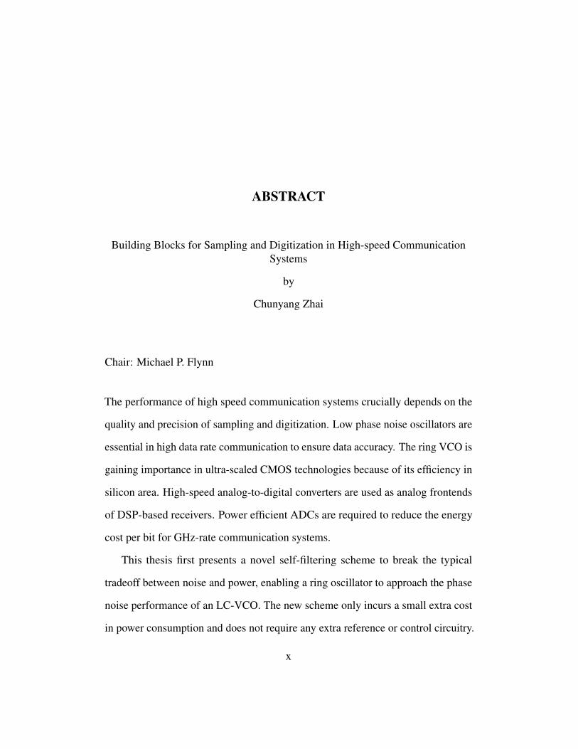
The performance of high speed communication systems crucially depends on the
quality and precision of sampling and digitization. Low phase noise oscillators are
essential in high data rate communication to ensure data accuracy. The ring VCO is
gaining importance in ultra-scaled CMOS technologies because of its efficiency in
silicon area. High-speed analog-to-digital converters are used as analog frontends
of DSP-based receivers. Power efficient ADCs are required to reduce the energy
cost per bit for GHz-rate communication systems.
This thesis first presents a novel self-filtering scheme to break the typical
tradeoff between noise and power, enabling a ring oscillator to approach the phase
noise performance of an LC-VCO. The new scheme only incurs a small extra cost
in power consumption and does not require any extra reference or control circuitry.
x
The prototype N-path filter enhanced VCO (NPFRVCO) achieves a measured phase
noise of -110 dBc/Hz at a 1 MHz offset frequency for an oscillation frequency of
1.0 GHz. This is more than a 10 dB improvement over a comparable fabricated
prototype structure without N-path filtering.
A new traveling wave pipeline ADC is also proposed that simultaneously
achieves the maximum sampling rate and high efficiency. The scheme exploits the
delay of on-chip transmission lines to implement a pipeline, and thereby avoids
the use of power hungry track-and-hold or MDAC stages. High sampling rates are
achieved without using time interleaving, thus no interleaving calibration is needed,
making the system design far simpler. This fast energy-efficient ADC architecture
will facilitate and improve communication applications. The transmission line is
implemented with differential symmetric inductors. This differential structure not
only benefits from the mutual inductance, but is also more realistic for integration
since it saves silicon area. The prototype is measured at 4.0 GS/s and 6.0 GS/s
sampling clock rate. SNDR of 21.35 dB and 18.8 dB is measured, respectively.
The prototype consumes 38.2 mW, and occupies 0.65 mm2.
xi
CHAPTER I
Introduction
1.1 High-speed Communication Systems
High-speed communication systems enable global interaction between people
from different nations and from different places on earth. Advances in communica-
tion technology and semiconductor fabrication technology have led to exponential
growth in the speed and capacity of communication systems. At the same time,
many of todays applications such as remote video meeting and on-line streaming
have pushed the needs for bandwidth.
1.1.1 The Growth of High-speed Communication Systems
Based on the CTIA - The Wireless Association’s annual wireless industry
survey [9], the number of wireless subscriber connections has increased from 207.9
million in 1995 to 377.9 million in 2015, an 82% increase over the past ten years.
This rapid growth of the mobile market has made wireless communication a market
1
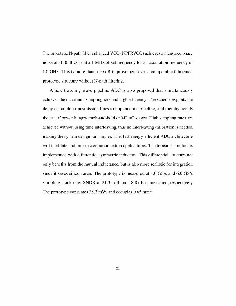
Figure 1.1 5G applications [1]
worth $200 billion annually.
The 5th generation wireless systems (abbreviated 5G) are the proposed next
generation communication systems to meet the significantly expanding connectivity
needs, as shown in Figure 1.1 [1]. The higher capacity of 5G allows a higher
number of mobile broadband connections per area unit. This makes it feasible
for 5G to enhance existing application and enable new applications. For example,
extreme mobile broadband applications, such as cloud storage and augmented
reality for entertainment, are driving the requirements for 5G. People can remotely
control diverse automated electronic devices with 5G equipped smart homes or
buildings. Due to the higher capacity of 5G, demanding indoor and outdoor
2
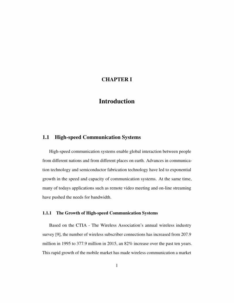
Figure 1.2 High speed links inside a router [2]
conditions such as crowded football stadium will not be a problem. 5G also
supports autonomous vehicles and object tracking, starting with Cellular Vehicle
to Everything (C-V2X) technologies that satisfy the 3rd generation partnership
project (3GPP) specifications. Moreover, wireless communication systems are
becoming increasingly important for industrial applications. Thanks to the low
latency and very low error rates, 5G technologies are useful for remote control of
critical infrastructure and process automation.
The surging demand for internet-enabled data center/devices, and cloud net-
working has led to high-speed wireline communication systems to support data
traffic at several Gbps. Figure 1.2 shows a router that uses an Ethernet cable to
connect to a modem [2]. There are 8 to 16 line cards in the router to serve as
input/output ports and data link processing. The switch cards execute the routing
protocols and perform network management. In this system, the chip-to-chip data
speed is 10 Gb/s and the laser driver link speed is 40 Gb/s to supply the four-serial
3
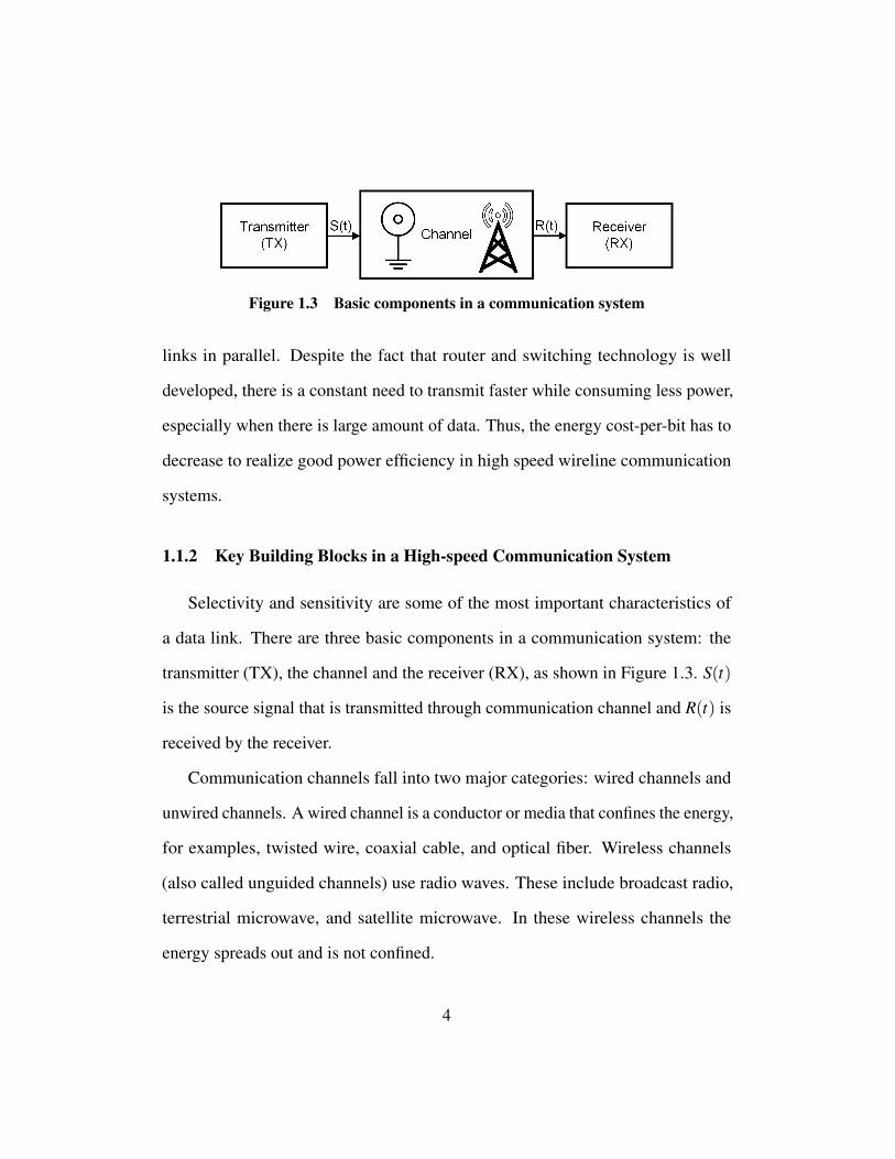
Figure 1.3 Basic components in a communication system
links in parallel. Despite the fact that router and switching technology is well
developed, there is a constant need to transmit faster while consuming less power,
especially when there is large amount of data. Thus, the energy cost-per-bit has to
decrease to realize good power efficiency in high speed wireline communication
systems.
1.1.2 Key Building Blocks in a High-speed Communication System
Selectivity and sensitivity are some of the most important characteristics of
a data link. There are three basic components in a communication system: the
transmitter (TX), the channel and the receiver (RX), as shown in Figure 1.3. S(t)
is the source signal that is transmitted through communication channel and R(t) is
received by the receiver.
Communication channels fall into two major categories: wired channels and
unwired channels. A wired channel is a conductor or media that confines the energy,
for examples, twisted wire, coaxial cable, and optical fiber. Wireless channels
(also called unguided channels) use radio waves. These include broadcast radio,
terrestrial microwave, and satellite microwave. In these wireless channels the
energy spreads out and is not confined.
4

Figure 1.4 Superheterodyne receiver (a) and transitter (b)
Figure 1.4 shows a superheterodyne wireless receiver (a) and transmitter (b).
In a receiver (Figure 1.4(a)), the RF filter selects the desired band. A low noise
amplifier (LNA) amplifies the signal to be detected. A mixer and local oscillator
(LO) down-convert the incoming radio frequency signal (RF) signal to a relatively
lower Intermediate Frequency (IF). An IF bandpass filter further separates out the
desired signal from signals that are close in frequency. After bandpass selection, an
IF amplifier amplifies the signal for demodulation. The output of the demodulator
is processed by the baseband digital circuitry. Converting the signal to IF has
several advantages. Firstly, it is feasible to convert signals at various frequencies
within a fixed frequency range by tuning the LO frequency. This can alleviate
the tunability requirements of subsequent stages such as filters and amplifiers.
Secondly, in general a filters bandwidth increases proportionally with its center
5

frequency for the same frequency-response. For a lower center frequency, a
narrower bandwidth can be achieved, thus more filter selectivity. Thirdly, there is
upper limit on the transition frequency of transistors that are used to perform signal
processing. As the speed of communication systems gets higher (several GHz),
transistors cannot provide enough gain to directly process a high-speed RF signal.
Besides, without converting to IF, expensive high frequency techniques such as
stripines and waveguides should be employed. In a superheretodyne transmitter
(Figure 1.4(b)) baseband signals are processed and then upconverted by mixer. The
mixer is controlled by the tunable oscillator, LO. Before the signal reaches the
antenna, it is amplified by a linear power amplifier and bandpass filtered by an RF
filter.
The data rates of wireless communication systems have increased dramatically
over the past twenty years. The wireless local area network (WLAN) standard
802.11b (in 1999) data rate is 11 Mb/s and the 802.11ac (in 2013) data rate is up
to 866 Mb/s [10]. New modulation formats, such as OFDM and pulse position
modulation, have been developed to make higher data rates feasible. The carrier
frequency has increased from 2.4 GHz in 802.11b to 5 GHz in 802.11a. 802.11ad
uses a 60 GHz carrier and supports data rates is up to 6.75 Gb/s.
Figure 1.5 shows the transmitter, channel and receiver in a high-speed link
system. The receiver must recover both the data and timing of the incoming
signal and often has two detectors: one is the slicer for data, and the other is the
phase-detector (PD) for timing recovery [3].
In ultra-scaled CMOS technology, digital signal processing implements most
6

Figure 1.5 High speed link system [3]
of the processing in modern, high-speed communication systems. This has led
to ADCs becoming the bottleneck in the scaling and performance of transceivers.
High-speed, high-precision ADCs are needed for high-dynamic-range applications.
However, these ADCs are too costly and power hungry. Moreover, it is difficult
to generate precise sampling clocks required for high speed ADCs to have opti-
mal performance. Random clock jitter degrades signal-to-noise ratio (SNR) and
increases the noise floor. Data dependent clock jitter results frequency spurs and
increases distortion in the ADCs output.
Clock signals not only serve as the sampling clock in ADCs, but also are
the heartbeat of many high-speed communication systems. Given the significant
processing that is dependent on a good clean clock, the phase noise performance
of clocks is critical for multi-gigabit data rate transmission.
7
1.2 Contributions
Designing building blocks for high-speed communication systems is challeng-
ing due to the many design tradeoffs that need to be considered, including circuit
complexity, power and area efficiencies, and phase noise performance. A sim-
ple block design with low complexity is critical. Complex designs result in a
longer design cycle and a higher possibility of implementation flaws. Therefore,
commonly employed structures in a high-speed block such as a time-interleaving
structure in high-speed ADCs are unattractive because of the need for complicated
calibration circuits. In addition, power and area efficiency are essential to reduce
the cost of a high-speed communication system. To achieve these, power-hungry
structures such as sample-and-hold and Multiplying DAC (MDAC) need to be
avoided in ahigh-speed ADC, and area-efficient clock generation blocks such as
the ring VCO (RVCO) should be considered. Last but not least, having a low phase
noise high-speed clock is important for signal purity. However, low phase noise
performance is usually at the cost of high power consumption in RVCO designs.
Therefore, it is important to research the design of low phase noise oscillators that
also have acceptable power consumption.
This thesis focuses on solving the design challenges of high-speed commu-
nication systems mentioned above. First of all, a novel self-filtering scheme is
proposed for a ring oscillator to break the typical tradeoff between phase noise
performance and power consumption. This newly proposed design enables the
phase noise performance of a ring VCO to approach that of an LC-VCO, without
8
any extra reference or control circuitry, and introduces only a small amount of extra
power consumption. To study the performance of the proposed scheme, a prototype
N-path filter enhanced VCO (NPFRVCO) is implemented in TSMC CMOS 65nm
technology. This NPFRVCO achieves a measured phase noise of -110 dBc/Hz at a
1 MHz offset frequency for an oscillation frequency of 1.0 GHz. This is more than
a 10 dB improvement over a comparable fabricated prototype structure without
N-path filtering.
Secondly, a new traveling wave pipeline ADC is proposed to simultaneously
achieve the maximum sampling rate and high power and area efficiencies. To
reduce the design complexity, the maximum ADC sampling rates are achieved
without using time interleaving. Also calibration circuits are avoided. In addition,
the proposed ADC improves the power efficiency by leveraging the delay of on-chip
transmission lines to implement a pipeline, which avoids the need for power-hungry
track-and-hold or MDAC stages. The transmission lines are implemented with
differential symmetric inductors that not only benefit from the mutual inductance,
but also are more area efficient for integration. A prototype ADC is taped out
in TSMC CMOS 40 nm technology. It is measured at sampling clock rates of
4.0 GS/s and 6.0 GS/s. The measured power consumption is 38.2 mW and the
die area is 0.65 mm2 area. An SNDR of 21.35 dB and 18.8 dB is measured,
for 4.0 GS/s and 6.0 GS/s, respectively. With its high speed and relatively low
power consumption, this proposed ADC architecture will facilitate and empower
high-speed communication systems.
9

1.3 Organization
The rest of this dissertation is organized as follows. Chapter II gives some
background on the voltage-controlled oscillators and high-speed ADCs. Chapter III
describes the design of an N-path filter enhanced low phase noise ring VCO and
demonstrates its power efficiency along with its low phase noise performance.
Chapter IV describes a traveling-wave ADC, which leverages the delay of on-chip
transmission lines and accomplishes both the maximum sampling rate and high
power efficiency. Future work is proposed in Chapter V. Finally, Chapter VI
concludes the dissertation.
10

CHAPTER II
Background
2.1 Oscillators in High-speed Communication Systems
In both wireless superheterodyne receivers and direct-conversion receivers, a
local oscillator (LO) drives a mixer to down-convert the frequency of the incoming
radio-frequency signal. In a wireless transmitter, an LO is often used to tune
the frequency of output signal. In data link receivers, phase-locked loops (PLL)
generate clock signals to capture and align data received over impaired channels.
In other applications, such as a chirp generator for radar system, the oscillator
is rapidly swept over a certain frequency range. In high-speed communications
systems, low phase noise oscillators are critical because they directly impact the
signal-to-noise ratio of high-speed ADCs and bit-error rate in high-speed data
transmission applications.
11

Figure 2.1 Resource block defination in frequency domain-LTE [4]
2.1.1 Voltage-controlled Oscillators
An oscillator produces a periodic oscillating signal that is either sine wave or
square wave. There are two categories of oscillators in high speed communication
systems: crystal oscillators and tuned oscillators (LC or RC oscillators). A crystal
oscillator, whose oscillation frequency is determined by the piezoelectric crystal
(commonly a quartz crystal), has good temperature stability and good phase noise
performance because the crystal functions as a very high Q-factor mechanical
resonator. However, since the frequency of crystal oscillator is mostly fixed,
changing the frequency requires physical changes in the crystal. Moreover, modern
wireless communication systems require tunable oscillators. For example, Long
Term Evolution (LTE) is a widely adopted standard for the fourth-generation
high-speed wireless communication. An LTE band consists of many small spaced
frequency channels called subcarriers, and these subcarriers are spaced 15 kHz
12
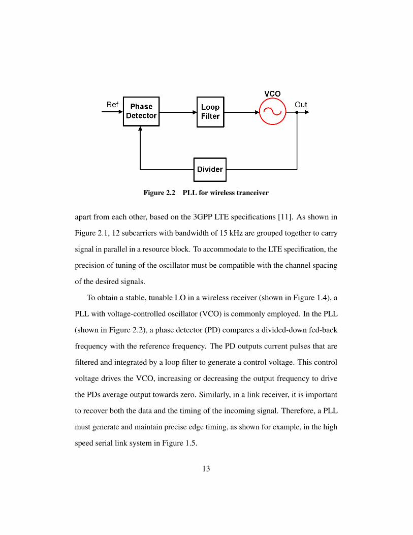
Figure 2.2 PLL for wireless tranceiver
apart from each other, based on the 3GPP LTE specifications [11]. As shown in
Figure 2.1, 12 subcarriers with bandwidth of 15 kHz are grouped together to carry
signal in parallel in a resource block. To accommodate to the LTE specification, the
precision of tuning of the oscillator must be compatible with the channel spacing
of the desired signals.
To obtain a stable, tunable LO in a wireless receiver (shown in Figure 1.4), a
PLL with voltage-controlled oscillator (VCO) is commonly employed. In the PLL
(shown in Figure 2.2), a phase detector (PD) compares a divided-down fed-back
frequency with the reference frequency. The PD outputs current pulses that are
filtered and integrated by a loop filter to generate a control voltage. This control
voltage drives the VCO, increasing or decreasing the output frequency to drive
the PDs average output towards zero. Similarly, in a link receiver, it is important
to recover both the data and the timing of the incoming signal. Therefore, a PLL
must generate and maintain precise edge timing, as shown for example, in the high
speed serial link system in Figure 1.5.
13
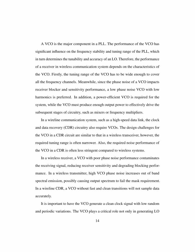
A VCO is the major component in a PLL. The performance of the VCO has
significant influence on the frequency stability and tuning range of the PLL, which
in turn determines the tunability and accuracy of an LO. Therefore, the performance
of a receiver in wireless communication system depends on the characteristics of
the VCO. Firstly, the tuning range of the VCO has to be wide enough to cover
all the frequency channels. Meanwhile, since the phase noise of a VCO impacts
receiver blocker and sensitivity performance, a low phase noise VCO with low
harmonics is preferred. In addition, a power-efficient VCO is required for the
system, while the VCO must produce enough output power to effectively drive the
subsequent stages of circuitry, such as mixers or frequency multipliers.
In a wireline communication system, such as a high-speed data link, the clock
and data recovery (CDR) circuitry also require VCOs. The design challenges for
the VCO in a CDR circuit are similar to that in a wireless transceiver, however, the
required tuning range is often narrower. Also, the required noise performance of
the VCO in a CDR is often less stringent compared to wireless systems.
In a wireless receiver, a VCO with poor phase noise performance contaminates
the receiving signal, reducing receiver sensitivity and degrading blocking perfor-
mance. In a wireless transmitter, high VCO phase noise increases out of band
spectral emission, possibly causing output spectrum to fail the mask requirement.
In a wireline CDR, a VCO without fast and clean transitions will not sample data
accurately.
It is important to have the VCO generate a clean clock signal with low random
and periodic variations. The VCO plays a critical role not only in generating LO
14
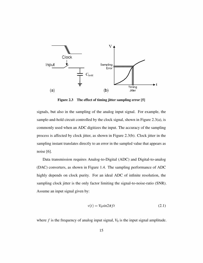
Figure 2.3 The effect of timing jitter sampling error [5]
signals, but also in the sampling of the analog input signal. For example, the
sample-and-hold circuit controlled by the clock signal, shown in Figure 2.3(a), is
commonly used when an ADC digitizes the input. The accuracy of the sampling
process is affected by clock jitter, as shown in Figure 2.3(b). Clock jitter in the
sampling instant translates directly to an error in the sampled value that appears as
noise [6].
Data transmission requires Analog-to-Digital (ADC) and Digital-to-analog
(DAC) converters, as shown in Figure 1.4. The sampling performance of ADC
highly depends on clock purity. For an ideal ADC of infinite resolution, the
sampling clock jitter is the only factor limiting the signal-to-noise-ratio (SNR).
Assume an input signal given by:
v(t) =V0sin2π f t (2.1)
where f is the frequency of analog input signal, V0 is the input signal amplitude.
15

The RMS value of dv/dt can be obtained:
dv/dt|rms = 2π fV0/√
2 (2.2)
Let ∆e = the voltage error and ∆t = the timing error, solving for ∆e:
∆e = 2π fV0∆t/√
2 (2.3)
The SNR due to clock jitter is given by [5]:
SNR = 20log(V0√
2∆e
) = 20log(V0√
22π fV0t j/
√2) = 20log(
12π f t j
) (2.4)
where t j is the variance of the timing error, f s the frequency of analog input signal.
This relationship is plotted in Figure 2.4 [6] and shows that the phase noise of
the sampling clock in any sampled data system is important, especially for higher
analog input frequencies.
2.1.2 Two Types of Voltage-controlled Oscillators
There are two common types of VCOs, LC-VCO and ring VCOs. Figure 2.5
shows an equivalent circuit of an LC-VCO. An inductor and capacitor are connected
in parallel to form a resonator. A transconductance (gm) is connected in positive
feedback to synthesize a negative resistance, Ramp. This negative resistance
cancels the parasitic resistance (Rp) of the resonant tank and initiates and sustains
the oscillation. LC oscillators are widely employed because of their low phase
16
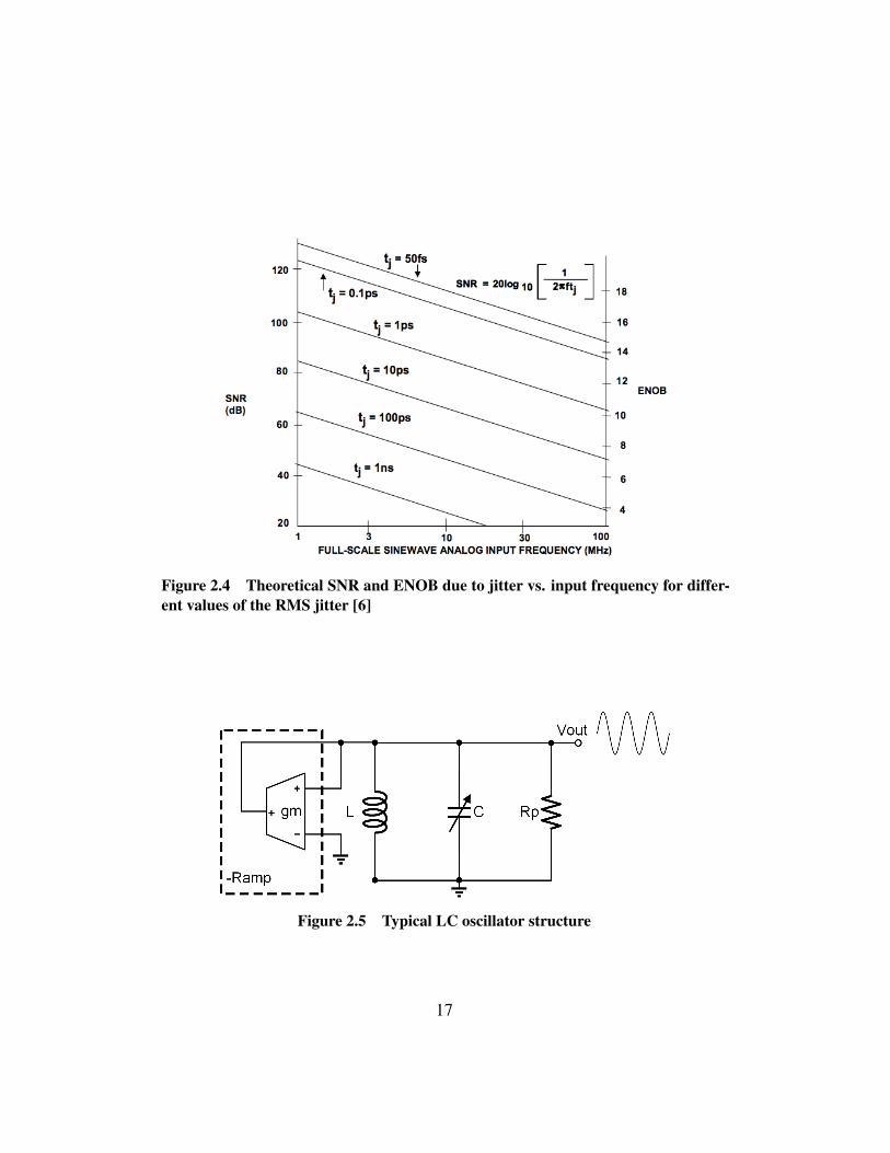
Figure 2.4 Theoretical SNR and ENOB due to jitter vs. input frequency for differ-ent values of the RMS jitter [6]
Figure 2.5 Typical LC oscillator structure
17
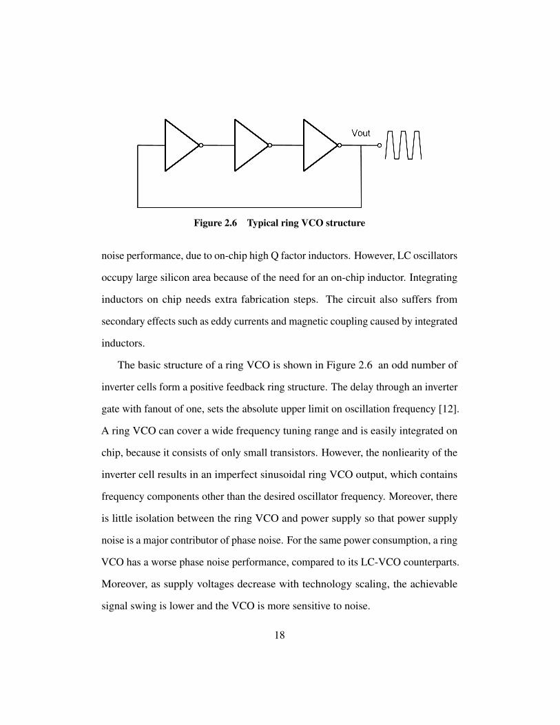
Figure 2.6 Typical ring VCO structure
noise performance, due to on-chip high Q factor inductors. However, LC oscillators
occupy large silicon area because of the need for an on-chip inductor. Integrating
inductors on chip needs extra fabrication steps. The circuit also suffers from
secondary effects such as eddy currents and magnetic coupling caused by integrated
inductors.
The basic structure of a ring VCO is shown in Figure 2.6 an odd number of
inverter cells form a positive feedback ring structure. The delay through an inverter
gate with fanout of one, sets the absolute upper limit on oscillation frequency [12].
A ring VCO can cover a wide frequency tuning range and is easily integrated on
chip, because it consists of only small transistors. However, the nonliearity of the
inverter cell results in an imperfect sinusoidal ring VCO output, which contains
frequency components other than the desired oscillator frequency. Moreover, there
is little isolation between the ring VCO and power supply so that power supply
noise is a major contributor of phase noise. For the same power consumption, a ring
VCO has a worse phase noise performance, compared to its LC-VCO counterparts.
Moreover, as supply voltages decrease with technology scaling, the achievable
signal swing is lower and the VCO is more sensitive to noise.
18
2.2 High Speed ADCs in High-speed Communication Systems
2.2.1 High Speed ADC Applications
Higher data bandwidths demanded by metro networks and data centers have
led to the deployment of very high data rates (10 Gb/s) wireless and wireline com-
munication systems. A number of standards have been developed to support high
bandwidth communication systems, including 10G Ethernet [11], over both fiber
and copper media. The data channels range from short optical and electrical links
within a data center, to long optical fibers connecting these data centers together.
Under severe channel impairments, a flexible receiver with a DSP backend provides
robust performance. DSP-based receivers incorporate sophisticated equalization
and timing recovery techniques, while allowing for better power and area scaling
with technology. A key block for such a receiver is the frontend ADC that digitizes
the incoming signal. Running at more than the aggregate data rate, the ADC
has to provide sufficient resolution under reasonable power dissipation and area
constraints [13] [14].
2.2.2 High Speed ADC Techniques
High-resolution digitizion of high-speed signals requires an ADC with good
sampling performance. For a Nyquist frequency ADC, the sampling clock fre-
quency must at least be two times greater than the analog input frequency to
generate a true representation of the high-speed analog input. Jitter in the high-
speed sampling clock causes uncertainty in actual sampling time. This results in
19
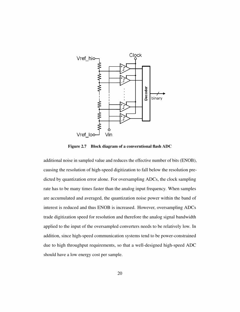
Figure 2.7 Block diagram of a converntional flash ADC
additional noise in sampled value and reduces the effective number of bits (ENOB),
causing the resolution of high-speed digitization to fall below the resolution pre-
dicted by quantization error alone. For oversampling ADCs, the clock sampling
rate has to be many times faster than the analog input frequency. When samples
are accumulated and averaged, the quantization noise power within the band of
interest is reduced and thus ENOB is increased. However, oversampling ADCs
trade digitization speed for resolution and therefore the analog signal bandwidth
applied to the input of the oversampled converters needs to be relatively low. In
addition, since high-speed communication systems tend to be power-constrained
due to high throughput requirements, so that a well-designed high-speed ADC
should have a low energy cost per sample.
20
Figure 2.8 Block diagram of a converntional SAR ADC
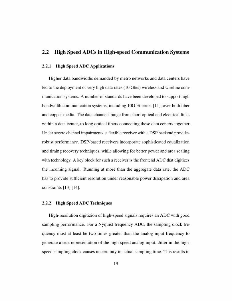
Flash ADCs, SAR ADCs and pipeline ADCs are the most common ways of
implementing a Nyquist frequency ADC. An n-bit flash ADC has comparators
and one reference ladder, as shown in Figure 2.7. Flash ADCs directly sample the
anlog input and compare the input signal with references generated by the linear
reference ladder. The flash ADC is the most parallel data converter structure, and
completes an entire conversion within one clock cycle.
Instead of using a large number of comparators, a SAR ADC is comprised of
a sample-and-hold circuit, a comparator, a DAC and a SAR logic control circuit,
as shown in Figure 2.8. The front-end sample-and-hold circuit samples and holds
the input signal. In each comparison cycle, the comparator compares the sampled
data with the DAC voltage, then the output of the comparator triggers that SAR
logic control circuit. According to the SAR logic, the DAC changes the reference
voltage. The cycle repeats until all the bits are determined [15].
Unlike flash ADCs and SAR ADCs which pose stringent requirements on all
circuit components, pipeline ADCs cascade several stages that are low resolution to
21

Figure 2.9 Block diagram of a pipeline ADC
achieve a high overall resolution, as shown in Figure 2.9. In each stage, a sub-ADC
digitizes the sampled input signal, then passes this digital output to sub-DAC which
converts the digital output back to an analog representation. After subtracting
this analog representation from the original sampled input signal, the residue is
amplified and sent to the next stage.
A delta-sigma ADC (shown in Figure 2.10), the most popular oversampling
ADC, consists of the delta-sigma modulator and the digital/decimation filter. The
delta-sigma modulator digitizing the inputs signal at very high frequency and
produces a 1-bit stream. The delta-sigma modulator implements noise shaping
so that the low frequency quantization noise is pushed up to higher frequencies,
outside the band of interest. The digital/decimation filter converts the sampled
1-bit stream into a high-resolution, slower digital output [16].
The very high sample rates required for high bandwidth applications can be
achieved in two ways. First, a single-channel moderate-resolution ADC with
22
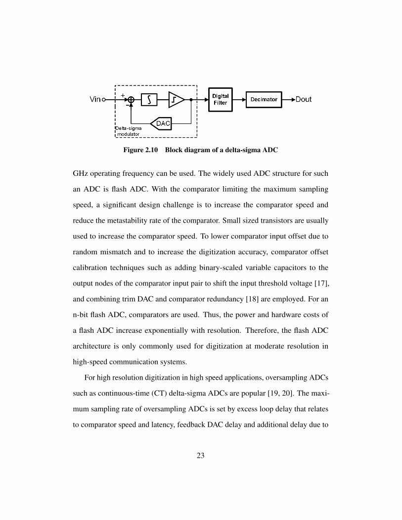
Figure 2.10 Block diagram of a delta-sigma ADC
GHz operating frequency can be used. The widely used ADC structure for such
an ADC is flash ADC. With the comparator limiting the maximum sampling
speed, a significant design challenge is to increase the comparator speed and
reduce the metastability rate of the comparator. Small sized transistors are usually
used to increase the comparator speed. To lower comparator input offset due to
random mismatch and to increase the digitization accuracy, comparator offset
calibration techniques such as adding binary-scaled variable capacitors to the
output nodes of the comparator input pair to shift the input threshold voltage [17],
and combining trim DAC and comparator redundancy [18] are employed. For an
n-bit flash ADC, comparators are used. Thus, the power and hardware costs of
a flash ADC increase exponentially with resolution. Therefore, the flash ADC
architecture is only commonly used for digitization at moderate resolution in
high-speed communication systems.
For high resolution digitization in high speed applications, oversampling ADCs
such as continuous-time (CT) delta-sigma ADCs are popular [19, 20]. The maxi-
mum sampling rate of oversampling ADCs is set by excess loop delay that relates
to comparator speed and latency, feedback DAC delay and additional delay due to
23
parasitics.
In order to achieve very high sample-rates, an alternative solution is to use
several lower sample-rate ADCs in a time-interleaved (TI) configuration. The
TI approach uses several sub-ADCs that quantize the input signal at a fraction
of the overall conversion speed and sample the input in a sequential manner.
This approach increases the design complexity because compensation for timing
misalignment and bandwidth mismatch of the sub-ADCs is often required. A
further challenge is to achieve the lowest possible latency. The TI approach
allows for a variety of sub-ADC architectures to be used, such as Flash ADCs,
Successive approximation (SAR) ADCs and Pipeline ADCs, depending on specific
requirements such as power dissipation, latency and silicon cost.
Because of their high conversion rate, flash ADCs are not only used for single
channel high speed applications but are also popular in TI structures. As flash ADCs
suffer from area and power penalties with increasing resolution; [13] employs
a rectifying flash ADC architecture that rectifies the input signal based on the
decision of a MSB comparator, thereby allowing the number of comparators to
be halved. There are various digital calibration circuits to optimize the ADC path
performance, including resistor calibration, offset calibration, gain adjustment and
phase alignment. These calibration circuits greatly increase the design complexity.
In addition to flash ADCs, SAR ADCs are among the most popular sub-ADC
structures. This SAR ADC architecture typically generates one bit per clock cycle
and has the benefit of a relatively small area, which is helpful in a highly interleaved
ADC. As in [14], with interleaving ratio of 8, each SAR is made of a compact
24

comb capacitor array, a comparator and 6-bit registers. The active area is only
0.009 mm2.
Pipeline ADCs are also commonly used as sub-ADCs, especially for high
resolution applications [21, 22, 23]. Pipeline ADCs achieve a high throughput
thanks to pipelining. When a stage decision is made, and the residue from this
stage is passed to the next stage, the current stage can then start processing the
next sample. The pipeline process is achieved with a multiplying DAC (MDAC)
that combines the functions of sample-and-hold, subtraction, DAC, and gain into
a single switched capacitor circuit, shown in Figure 2.9. Requirements such as
timing matching and sampling accuracy are only critical when resolving the most
significant bits (MSBs). Therefore, pipeline ADCs are more attractive as sub-ADCs
than SAR ADCs in terms of design complexity and power efficiency, especially
when high resolution and high convertion speed are demanded. The MDAC is the
most power-hungry block in pipeline ADC. One approach to reduce the power
consumption of pipeline ADC is to avoid using a sample-and-hold. amplifier
(SHA) in the MDAC [24].
Figure 2.11 shows a summary plot of Walden FoM of state-of-art high speed
(>5 GS/s) ADCs based on ADC survey [25]. It can be concluded that the TI
structure is widely employed in high speed ADC designs; SAR ADCs and flash
ADCs are popular sub-ADCs in TI ADCs.
25

Figure 2.11 Walden FoM vs. sampling clock rate of ADCs
2.3 High Speed Sampling and Digitization
This research focuses on high-speed sampling and digitization which are chal-
lenging because many design tradeoffs are critical and inevitable. The first chal-
lenge is to design an energy-efficient high-speed ADC with the least complexity.
In order to reduce the power consumption, power hungry blocks such as sample-
and-hold and MDAC are avoided. To reduce design complexity, time-interleaving
is not used, so that complicated calibration circuits are not needed. Secondly, for a
given power consumption, a challenge is to generate a low phase noise high-speed
clock that is compatible with technology scaling. For area efficient oscillators such
as ring VCO, there is typical tradeoff between noise and power. The target of this
26
research is to enable a ring VCO to deliver the phase noise performance of an
LC-VCO, in this way achieving both high area efficiency and low energy cost.
27

CHAPTER III
An N-path Filter Enhanced Low Phase Noise Ring
VCO
3.1 Ring Voltage-controlled Oscillator
The reliability and the phase noise of an oscillator greatly affect system per-
formance. CMOS ring oscillators consume significantly less silicon area than
integrated LC-VCOs and do not require high quality factor inductors. They also
have the advantage of a much wider tuning and can easily generate multiple
phases [12]. However, LC oscillators offer better phase noise and are less sensitive
to supply noise. Recent research has concentrated on reducing the phase noise of
ring oscillators by modifying the delay cell to help make the ring oscillator less
sensitive to supply noise, such as in [26], where a source-follower-based delay
multipath ring oscillator is proposed. Others have achieved good in-band phase
noise in a ring oscillator with the reference phase alignment technique, such as
demonstrated in [27].
28
Figure 3.1 Power spectrum of RVCO and desired power spectrum of NPFRVCO
To achieve a better phase noise performance, the technique of band-pass fil-
tering around the oscillation frequency is widely applied. If the quality factor of
this filter is high enough, this helps the oscillator remove unwanted signal power
away from the carrier, as shown in the power spectral plot in Figure 3.1. There
have been several approaches to realize the band-pass filter based on inductors and
capacitors, such as in [28], where the LC band-pass filter provides sufficient phase
shift to tune to the oscillation frequency of the VCO and serves as the load to each
of the ring oscillator stages. These filters, however, tend to be large and suffer from
a limited tuning range. Instead, in this work, an N-path filter filters the output of
each ring and, injects the filtered output into the other ring. Unlike the scheme
in [28], our scheme does not require inductors and inherently tracks the oscillation
29
Figure 3.2 Low pass filter transformed to bandpass filter
Figure 3.3 N-path band-pass filter network
frequency of the VCO. As N-path filter characteristically has a narrow pass-band,
which is determined by its RC constant from low-pass filter on each path; as shown
in Figure 3.2, it suppresses the excess noise around the oscillator carrier frequency.
3.2 N-path Filter
A large bank of low-pass filters that are composed of resistors and capacitors,
is sampled in frequency with switched-capacitor network, as shown in Figure 3.3
(a) and (b) [29]. The non-overlapping control signals for switches are shown in
Figure 3.4 (a). If the second switches at the output are eliminated and the resistor
is placed in-between input and output, the circuit in Figure 3.3 (b) will transform to
30
Figure 3.4 Control signals for switches (a) and simplified N-path filter (b)
the circuit in Figure 3.4 (b). The frequency response of this filter looking in from
the input port is a band-pass function.
An N-path filter is comprised of N capacitors, connected in turn to the sig-
nal source through a resistor and one of N switches, and controlled by N non-
overlapping clock signals. The center frequency of the band-pass filter is at the
N-path clocking frequency. The band-pass filtering mechanism of an n-path filter
can be understood by considering an input test tone, exactly at the switching fre-
quency. In that case, because the switches operate at the same frequency as the
input frequency, the capacitor in each path samples the same input value every
time, so there is no attenuation. On the other hand, signals away from the clock
frequency are attenuated. From a spectral point of view, the N-path filter first
down-converts the input frequency, and then recovers the signal while suppressing
the portion of signal that is offset from the desired frequency; as a result, making
the N-path filter a very high Q band-pass filter [30]. Figure 3.5 shows an N-path
filter equivalent circuit. Bandwidth of this bandpass filter is decided by Rs and CL
31

Figure 3.5 N-path filter equivalent structure
if:
| fin− fclk|<1
RsCL(3.1)
3.3 NPFRVCO Circuit Implementation
The concept of the new low phase noise N-path filter assisted ring VCO is
shown in a block diagram in Figure 3.6. Two identical differential three-stage
ring oscillators (A and B) are cross-coupled through differential continuous time
band-pass N-path filters (FA and FB). The output of each ring oscillator is injected
to the other ring oscillator after it is filtered by the N-path filter and buffered.
By itself without filtering, the coupling of two oscillators should lead to a 3 dB
reduction in phase noise. Because coupling of two oscillators is equivalent to
doubling the size of the device and power consumption in one oscillator; the
32
Figure 3.6 NPRVCO block diagram
signal doubles in amplitude and the noise only doubles in power. This results in a
3 dB improvement in SNR. Thus the phase noise is inversely proportional to the
oscillator power consumption. There is a trade-off between phase noise and power
consumption. N-path band-pass filters are added to filter the injected coupling
signal to the coupled structure to further improve the overall phase noise, with only
a small power penalty. Minimizing the phase noise for a given power consumption
is achieved.
The N-path filter structure transfers a low-pass RC filter characteristic to a high
frequency bandpass filter to achieve a high Q. Because the resulting band-pass
filter has just twice the 3 dB bandwidth of the low-pass RC filter, an N-path filters
achieve a high Q using only resistors, capacitors and switches.
33
Figure 3.7 NPFRVCO implementation
Figure 3.7 shows a block diagram of coupled, N-path filtered oscillator system.
There are two three-path N-path filters for each oscillator. A differential buffer
follows the two N-path filters to generate the injection signals. The three non-
overlapping switch signals are conveniently derived from the outputs of a three-
stage ring oscillator with the help of a non-overlap clock generator. The overall
coupled oscillator is differential–a single ended version is shown for clarity.
The non-overlapping switch control signals are generated from the outputs
of each oscillator so that the switching frequency is the same as the oscillator
frequency, as shown in Figure 3.8. Similar to the conventional two phase non-
overlapping clock generator, this generator circuit consists of three coupled NAND
34
Figure 3.8 Non-overlapping clocks generator
gates. OUTA′1, OUTA′2 and OUTA′3 are the delayed outputs of ring A.SWA′1,
SWA′2 and SWA
′3 are the three generated non-overlapping clock phases. The
NAND gates are followed by the inverters with optimal sizing to delay the edge of
the clocks.
The tunable differential delay cell, shown in Figure 3.9, has a coarse-tuning
NMOS tail current cell and fine-tuning PMOS loads. The differential structure
is less sensitive to power supply noise. The inputs are connected to both NMOS
transistor and PMOS transistors. A latch follows the differential delay cell to speed
up signal transitions and convert the outputs to rail-to-rail signals. White noise in
the delay cell and flicker noise in the tuning current cell are main sources of phase
noise [12].
Figure 3.10 shows phase noise simulation results for NPFRVCO with different
capacitances in the N-path filters and also the phase noise simulation for a cross-
coupled oscillator without N-path filters. The phase noise is at 1 MHz offset from
35

Figure 3.9 Differential delay cell
carrier. As shown in the figure, an NPFRVCO with large capacitor load (the red
curve) in the N-path filters has better phase noise performance than the one with
a small capacitor load (the blue curve). Because an N-path filter with a larger
load capacitance has a larger time constant and therefore a narrower bandwidth,
it enables more phase noise reduction than the one with smaller capacitance. In
addition, both NPFRVCOs with N-path filters have better phase noise performance
than the cross-coupled oscillators without filters (the dotted line).
36
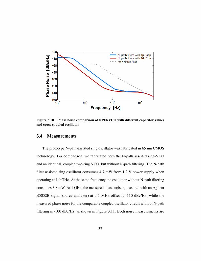
Figure 3.10 Phase noise comparison of NPFRVCO with different capacitor valuesand cross-coupled oscillator
3.4 Measurements
The prototype N-path-assisted ring oscillator was fabricated in 65 nm CMOS
technology. For comparison, we fabricated both the N-path assisted ring-VCO
and an identical, coupled two-ring VCO, but without N-path filtering. The N-path
filter assisted ring oscillator consumes 4.7 mW from 1.2 V power supply when
operating at 1.0 GHz. At the same frequency the oscillator without N-path filtering
consumes 3.8 mW. At 1 GHz, the measured phase noise (measured with an Agilent
E5052B signal source analyzer) at a 1 MHz offset is -110 dBc/Hz, while the
measured phase noise for the comparable coupled oscillator circuit without N-path
filtering is -100 dBc/Hz, as shown in Figure 3.11. Both noise measurements are
37
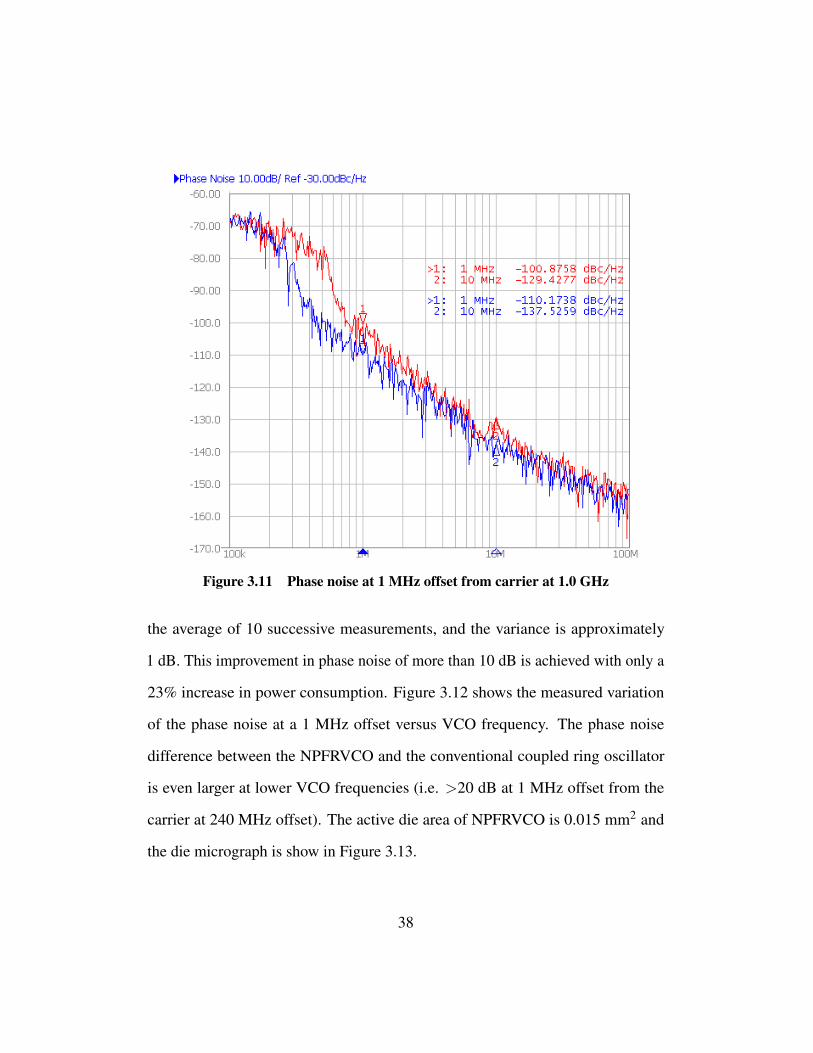
Figure 3.11 Phase noise at 1 MHz offset from carrier at 1.0 GHz
the average of 10 successive measurements, and the variance is approximately
1 dB. This improvement in phase noise of more than 10 dB is achieved with only a
23% increase in power consumption. Figure 3.12 shows the measured variation
of the phase noise at a 1 MHz offset versus VCO frequency. The phase noise
difference between the NPFRVCO and the conventional coupled ring oscillator
is even larger at lower VCO frequencies (i.e. >20 dB at 1 MHz offset from the
carrier at 240 MHz offset). The active die area of NPFRVCO is 0.015 mm2 and
the die micrograph is show in Figure 3.13.
38
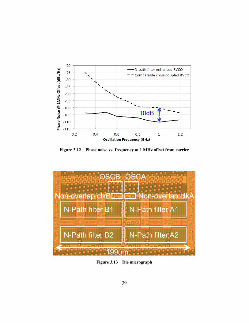
Figure 3.12 Phase noise vs. frequency at 1 MHz offset from carrier
Figure 3.13 Die micrograph
39
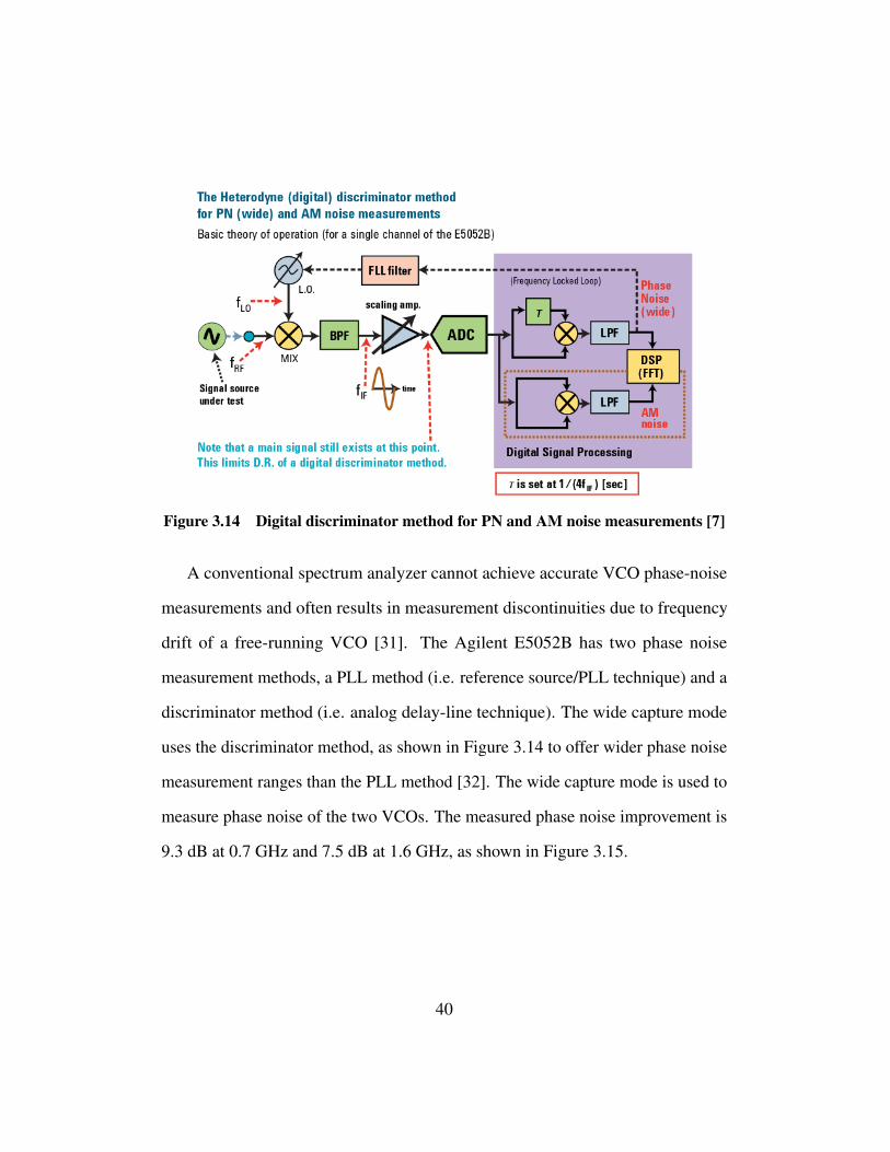
Figure 3.14 Digital discriminator method for PN and AM noise measurements [7]
A conventional spectrum analyzer cannot achieve accurate VCO phase-noise
measurements and often results in measurement discontinuities due to frequency
drift of a free-running VCO [31]. The Agilent E5052B has two phase noise
measurement methods, a PLL method (i.e. reference source/PLL technique) and a
discriminator method (i.e. analog delay-line technique). The wide capture mode
uses the discriminator method, as shown in Figure 3.14 to offer wider phase noise
measurement ranges than the PLL method [32]. The wide capture mode is used to
measure phase noise of the two VCOs. The measured phase noise improvement is
9.3 dB at 0.7 GHz and 7.5 dB at 1.6 GHz, as shown in Figure 3.15.
40
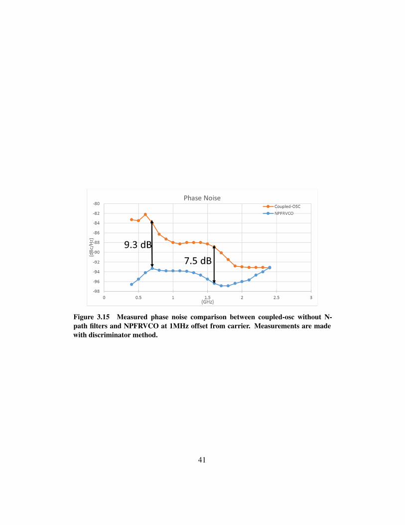
Figure 3.15 Measured phase noise comparison between coupled-osc without N-path filters and NPFRVCO at 1MHz offset from carrier. Measurements are madewith discriminator method.
41

CHAPTER IV
Traveling-Wave ADC
4.1 High Speed ADC with On-chip Transmission Line
This new ADC architecture is inspired by the RF traveling-wave amplifier
architecture. As shown in Figure 4.1, a distributed amplifier [8] has a pair of
transmission lines that are independently connected to the inputs and outputs.
The delays of the input and output lines are made equal. Similarly, in this very
high speed ADC, shown in Figure 4.2, an on-chip transmission line provides an
alternative approach to transmit clock and input signaling without needing power-
consuming active circuitry. A significant advantage is that high tracking bandwidth
sample-and-hold [33] amplifiers and MDACs are no longer needed to sample and
transmit input signal.
42
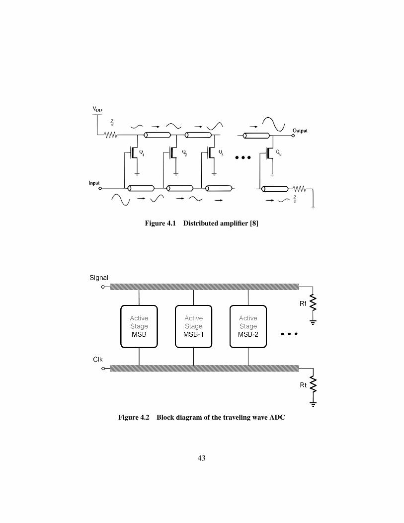
Figure 4.1 Distributed amplifier [8]
Figure 4.2 Block diagram of the traveling wave ADC
43
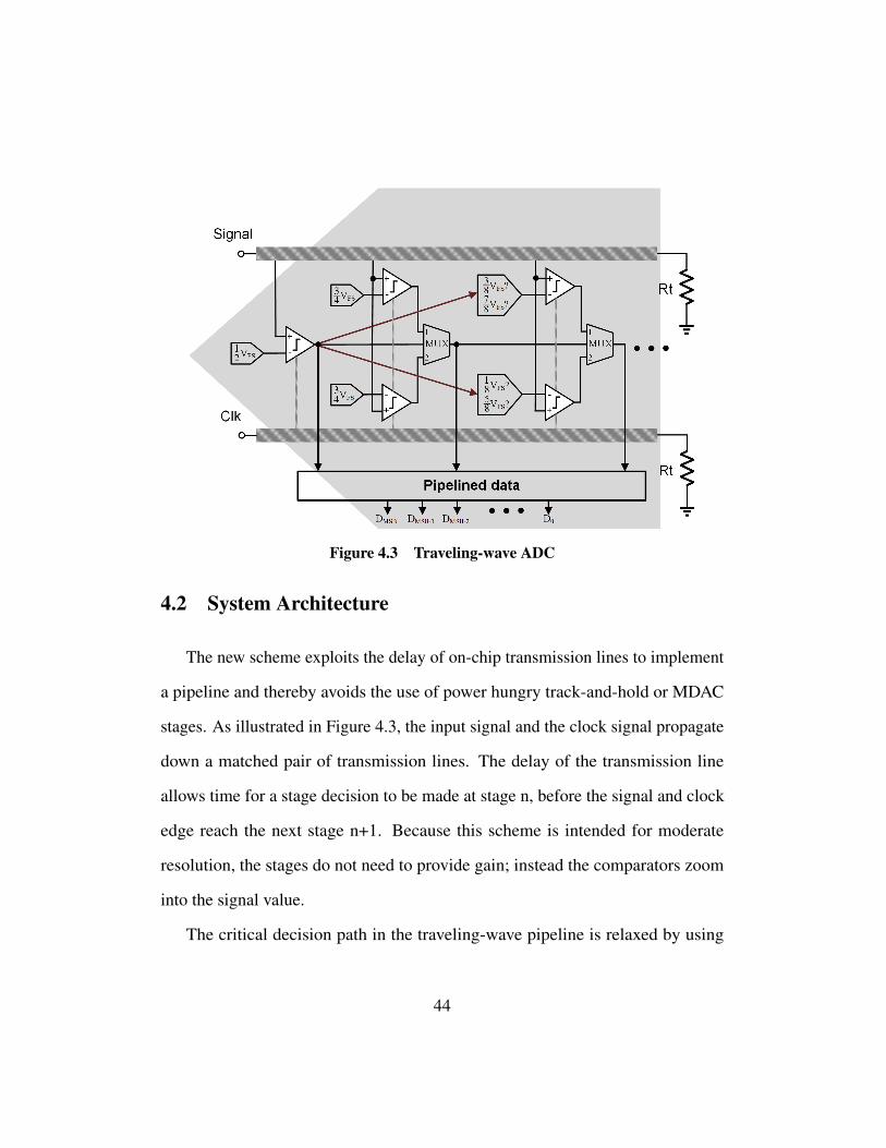
Figure 4.3 Traveling-wave ADC
4.2 System Architecture
The new scheme exploits the delay of on-chip transmission lines to implement
a pipeline and thereby avoids the use of power hungry track-and-hold or MDAC
stages. As illustrated in Figure 4.3, the input signal and the clock signal propagate
down a matched pair of transmission lines. The delay of the transmission line
allows time for a stage decision to be made at stage n, before the signal and clock
edge reach the next stage n+1. Because this scheme is intended for moderate
resolution, the stages do not need to provide gain; instead the comparators zoom
into the signal value.
The critical decision path in the traveling-wave pipeline is relaxed by using
44
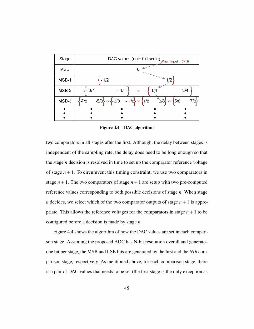
Figure 4.4 DAC algorithm
two comparators in all stages after the first. Although, the delay between stages is
independent of the sampling rate, the delay does need to be long enough so that
the stage n decision is resolved in time to set up the comparator reference voltage
of stage n+1. To circumvent this timing constraint, we use two comparators in
stage n+1. The two comparators of stage n+1 are setup with two pre-computed
reference values corresponding to both possible decisions of stage n. When stage
n decides, we select which of the two comparator outputs of stage n+1 is appro-
priate. This allows the reference voltages for the comparators in stage n+1 to be
configured before a decision is made by stage n.
Figure 4.4 shows the algorithm of how the DAC values are set in each compari-
son stage. Assuming the proposed ADC has N-bit resolution overall and generates
one bit per stage, the MSB and LSB bits are generated by the first and the Nth com-
parison stage, respectively. As mentioned above, for each comparison stage, there
is a pair of DAC values that needs to be set (the first stage is the only exception as
45
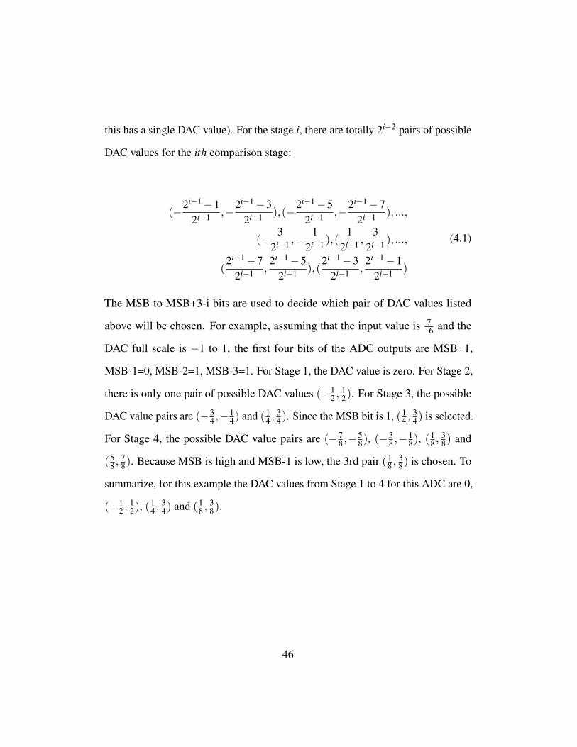
this has a single DAC value). For the stage i, there are totally 2i−2 pairs of possible
DAC values for the ith comparison stage:
(−2i−1−12i−1 ,−2i−1−3
2i−1 ),(−2i−1−52i−1 ,−2i−1−7
2i−1 ), ...,
(− 32i−1 ,−
12i−1 ),(
12i−1 ,
32i−1 ), ...,
(2i−1−7
2i−1 ,2i−1−5
2i−1 ),(2i−1−3
2i−1 ,2i−1−1
2i−1 )
(4.1)
The MSB to MSB+3-i bits are used to decide which pair of DAC values listed
above will be chosen. For example, assuming that the input value is 716 and the
DAC full scale is −1 to 1, the first four bits of the ADC outputs are MSB=1,
MSB-1=0, MSB-2=1, MSB-3=1. For Stage 1, the DAC value is zero. For Stage 2,
there is only one pair of possible DAC values (−12 ,
12). For Stage 3, the possible
DAC value pairs are (−34 ,−
14) and (1
4 ,34). Since the MSB bit is 1, (1
4 ,34) is selected.
For Stage 4, the possible DAC value pairs are (−78 ,−
58), (−
38 ,−
18), (
18 ,
38) and
(58 ,
78). Because MSB is high and MSB-1 is low, the 3rd pair (1
8 ,38) is chosen. To
summarize, for this example the DAC values from Stage 1 to 4 for this ADC are 0,
(−12 ,
12), (
14 ,
34) and (1
8 ,38).
46

4.3 System Implementation
4.3.1 On-chip Transmission Line
The on-chip transmission line must provide sufficient delay between stages. At
the same time the loss and dispersion of the line must be small. The frequency-
dependent complex transfer function H( f ) of a transmission line can be expressed
as:
H( f ) = A( f ) · exp jφ( f ) (4.2)
where A( f ) denominates the magnitude and φ( f ) is the phase response. Based on
phase simulation results and measurement results, we can find the group delay tgr
of the transmission line. tgr is the negative derivative of the phase φ (in degrees)
with respect to frequency f :
tgr =−1
360· dφ
d f(4.3)
For non-dispersive transmission lines, group delay is not a function of frequency at
all, but constant. Therefore, phase φ( f ) is a linear function of frequency:
φ( f ) =−360 · f · td (4.4)
Where, td is the delay time of the transmission line. From 4.3 and 4.4, since
phase is a linear function of frequency f , the delay time td and the group delay
tgr are equivalent. To measure the delay of the non-dispersive transmission line,
47
measurements of group delay can be performed. For accurate tracking of the
phase shift versus frequency, the frequency span and the number of points for the
network analyzer must be chosen so that the phase shift between each two adjacent
frequency points does not exceed 180. The delay time td is directly related to its
physical length Lphy of the transmission line, the light velocity in vacuum c; and
the equivalent dielectric constant around the transmission line εe f f :
td =Lphy ·
√εe f f
c(4.5)
The product Lphy ·√
εe f f denotes the effective length of the transmission line
as ’seen’ by the electrical signal traveling along the line. To make the on-chip
transmission line practical, we want the physical transmission line length Lphy to
be as short as possible. Meanwhile, since the comparator must decide based on
the previous decision, the delay provided by the transmission line should be long
enough to avoid decision errors. As the velocity of light c is a constant, to keep td
equal to the delay of comparator, a smaller Lphy requires an even larger εe f f .
The slow-wave transmission line structure proposed in Figure 4.5 increases
εe f f , therefore increasing the effective length of the transmission line and slowing
down the signal propagation speed in the transmission line. This can, in principle,
reduce the required length by an order of magnitude. To reduce the silicon cost and
make the layout more compact, we want to use the shortest possible transmission
line, thus requiring an even larger εe f f which furthermore increases the design
difficulty of the transmission line.
48
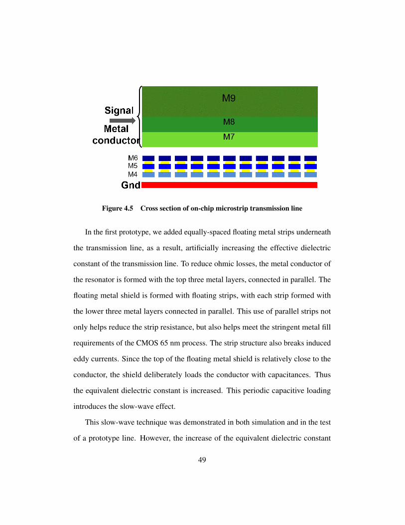
Figure 4.5 Cross section of on-chip microstrip transmission line
In the first prototype, we added equally-spaced floating metal strips underneath
the transmission line, as a result, artificially increasing the effective dielectric
constant of the transmission line. To reduce ohmic losses, the metal conductor of
the resonator is formed with the top three metal layers, connected in parallel. The
floating metal shield is formed with floating strips, with each strip formed with
the lower three metal layers connected in parallel. This use of parallel strips not
only helps reduce the strip resistance, but also helps meet the stringent metal fill
requirements of the CMOS 65 nm process. The strip structure also breaks induced
eddy currents. Since the top of the floating metal shield is relatively close to the
conductor, the shield deliberately loads the conductor with capacitances. Thus
the equivalent dielectric constant is increased. This periodic capacitive loading
introduces the slow-wave effect.
This slow-wave technique was demonstrated in both simulation and in the test
of a prototype line. However, the increase of the equivalent dielectric constant
49
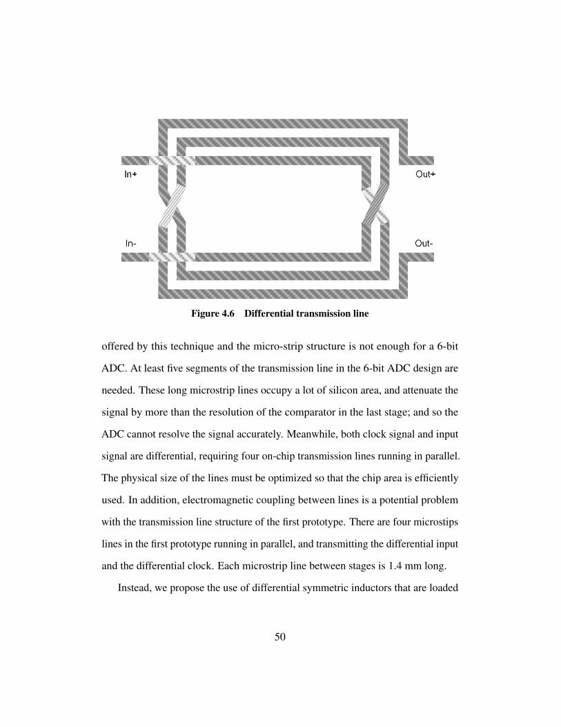
Figure 4.6 Differential transmission line
offered by this technique and the micro-strip structure is not enough for a 6-bit
ADC. At least five segments of the transmission line in the 6-bit ADC design are
needed. These long microstrip lines occupy a lot of silicon area, and attenuate the
signal by more than the resolution of the comparator in the last stage; and so the
ADC cannot resolve the signal accurately. Meanwhile, both clock signal and input
signal are differential, requiring four on-chip transmission lines running in parallel.
The physical size of the lines must be optimized so that the chip area is efficiently
used. In addition, electromagnetic coupling between lines is a potential problem
with the transmission line structure of the first prototype. There are four microstips
lines in the first prototype running in parallel, and transmitting the differential input
and the differential clock. Each microstrip line between stages is 1.4 mm long.
Instead, we propose the use of differential symmetric inductors that are loaded
50
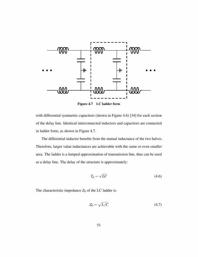
Figure 4.7 LC ladder form
with differential symmetric capacitors (shown in Figure 4.6) [34] for each section
of the delay line. Identical interconnected inductors and capacitors are connected
in ladder form, as shown in Figure 4.7.
The differential inductor benefits from the mutual inductance of the two halves.
Therefore, larger value inductances are achievable with the same or even smaller
area. The ladder is a lumped approximation of transmission line, thus can be used
as a delay line. The delay of the structure is approximately:
Td =√
LC (4.6)
The characteristic impedance Z0 of the LC ladder is:
Z0 =√
L/C (4.7)
51
Designed for a characteristic impedance Z0 = 50Ω, Td = 9 ps, we can calculate
Le f f = 450 pH and C = 180 f F . Thus the transmission line between stages
consists of four LC ladder segments that contribute a delay of 36 ps delay. The
impedance of the line versus frequency is:
Zω =
√LC·√
1− LCω2
4= Z0 ·
√1− LCω2
4(4.8)
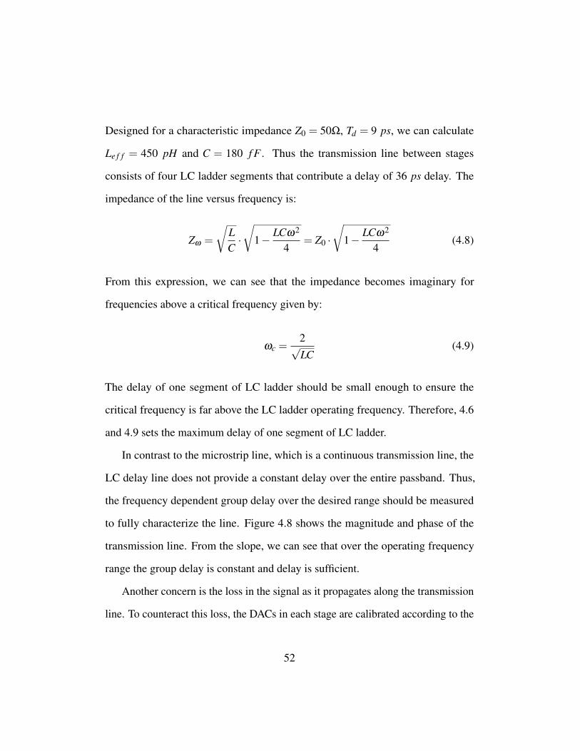
From this expression, we can see that the impedance becomes imaginary for
frequencies above a critical frequency given by:
ωc =2√LC
(4.9)
The delay of one segment of LC ladder should be small enough to ensure the
critical frequency is far above the LC ladder operating frequency. Therefore, 4.6
and 4.9 sets the maximum delay of one segment of LC ladder.
In contrast to the microstrip line, which is a continuous transmission line, the
LC delay line does not provide a constant delay over the entire passband. Thus,
the frequency dependent group delay over the desired range should be measured
to fully characterize the line. Figure 4.8 shows the magnitude and phase of the
transmission line. From the slope, we can see that over the operating frequency
range the group delay is constant and delay is sufficient.
Another concern is the loss in the signal as it propagates along the transmission
line. To counteract this loss, the DACs in each stage are calibrated according to the
52
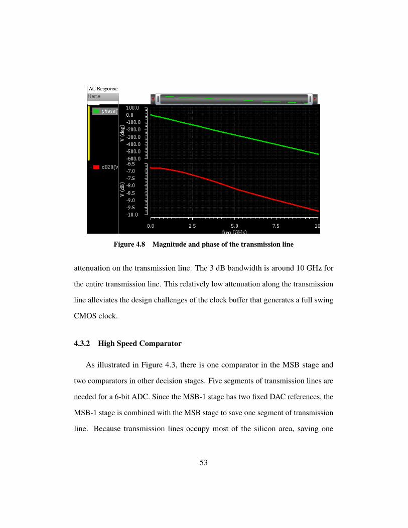
Figure 4.8 Magnitude and phase of the transmission line
attenuation on the transmission line. The 3 dB bandwidth is around 10 GHz for
the entire transmission line. This relatively low attenuation along the transmission
line alleviates the design challenges of the clock buffer that generates a full swing
CMOS clock.
4.3.2 High Speed Comparator
As illustrated in Figure 4.3, there is one comparator in the MSB stage and
two comparators in other decision stages. Five segments of transmission lines are
needed for a 6-bit ADC. Since the MSB-1 stage has two fixed DAC references, the
MSB-1 stage is combined with the MSB stage to save one segment of transmission
line. Because transmission lines occupy most of the silicon area, saving one
53
segment of transmission line reduces almost 20% of silicon cost. Moreover, the
signal is attenuated along the transmission lines. The signal received by the last
active stage will be less attenuated since the lines are shorter. This can alleviate the
requirements for resolution of the comparator in the last stage. However, combining
the first two stages results in only one transmission line delay for the MSB decision
to set the DACs references in the MSB-2 stage. To solve this issue, instead of
two comparators, four comparators with four possible DAC references are placed
in MSB-2 stage. Increasing the number of comparators to compensate for lack
of delay provided by the transmission line is a tradeoff between silicon cost and
power consumption. In conclusion, there are two comparators per decision stage,
one comparator in MSB stage and four comparators in the MSB-2 stage. The
peak-to-peak input range is 640 mV, resulting in a nominal LSB value of 10 mV. To
achieve a power-efficient design, dynamic comparators without any pre-amplifiers
are employed in this ADC.
Figure 4.9 shows the design of the comparator, which is based on a dynamic-
sense amplifier latch [35] incorporating several modifications. The comparator
consists of a double differential input stage and a regenerative latch at the output.
The input devices are sized small to minimize input capacitance. Because the
comparator input transistors are small, there are two 4-bit trim currents to calibrate
the comparator offsets [36]. The offset trimming circuit generates a current which
compensates the input device offset, such that the error after trimming is below
1/4 LSB. For all the comparators, offset calibration is done simultaneously during
startup. Two reset switches are employed to reset the gates and sources of the
54
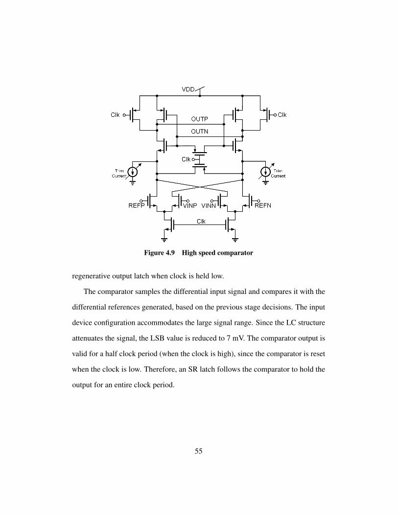
Figure 4.9 High speed comparator
regenerative output latch when clock is held low.
The comparator samples the differential input signal and compares it with the
differential references generated, based on the previous stage decisions. The input
device configuration accommodates the large signal range. Since the LC structure
attenuates the signal, the LSB value is reduced to 7 mV. The comparator output is
valid for a half clock period (when the clock is high), since the comparator is reset
when the clock is low. Therefore, an SR latch follows the comparator to hold the
output for an entire clock period.
55
4.3.3 Current-steering DAC
Current-steering DACs are normally implemented with a tail current source
and a pair of switches that are controlled by digital signals. Current steering
DACs produce and combine several scaled copies of a reference current. The
summed current is then converted to voltage with a pair of resistor loads. Current-
steering DACs mitigate the effects of mismatch and process variations with careful
arrangement of current cells while saving silicon cost by using compact devices
such as MOSFETs, instead of capacitors or resistors as unit current cell. Moreover,
the structure of current-steering DACs can be easily integrated with trim current
calibration technique. However, even with calibration there are still dynamic non-
idealities that need to be taken care of. For example, the finite settling time due
to RC time constants of the resistor loads and parasitic capacitors; the coupling
of control signals to the current DAC output though switch charge injection; and
timing error due to control signal timing skew.
To achieve faster settling time, the resistor loads in current-steering DACs are
chosen to be small. The DAC swing is set by the product of resistor load and
combined currents of the array of current cells. The minimum DAC swing is set
by the minimum voltage difference that the comparator can detect. For a fixed
DAC swing, if the resistor loads are small, the DAC should burn more current to
generate the same DAC swing. Thus, there is a tradeoff between fast settling time
and lower power consumption. To make sure the DAC references are ready for
comparators to make a decision, i.e. the settling time is longer than twice the RC
56

time constant (86% accuracy), the maximum settling time tsettle can be calculated
as:
tsettl = 2 ·Td−tline− tclk−q (4.10)
Where Td−tline is the delay provided by the transmission line between two stages
and tclk−q is the time it takes for the high speed comparator output to be in a stable
state after clock samples. Since the peak-to-peak input range is 640 mV, for a 6-bit
ADC with 64 conversions, the LSB size is 10 mV. The RMS noise voltage of the
high speed comparator is 2.34 mV, which is within the LSB size of current-steering
DACs. For a 100-ohm resistor load, the nominal LSB current is 0.1 mA.
These current DACs allow in-DAC summing, thereby eliminating the need for
high-speed digital logic in the critical path. The current-steering DAC consists of
binary weighted current cells driven by decision bits from previous stages. Each
current cell is composed of current source devices, cascode devices and switches.
For fast settling, a small cascode device isolates the large drain capacitance of the
current source device from switch devices. Figure 4.10 (a) and (b) shows the two
DACs in the stage MSB-2. Each DAC generates two differential signals that are
sent to the reference input nodes of the corresponding comparator. The current cell
with fixed control switches (VDD and VSS) in each DAC sets the resolution of the
DAC. Bit B0 and bit B0 are the complementary decision bits from stage MSB and
bit B1 and bit B1 are from stage MSB-1. These bits directly set the DAC outputs
in stage MSB-2 without extra high-speed logic. Figure 4.10 (c) shows the DACs
generate -3/4 and -1/4 of full input range for comparators when both B0 and B1 are
57

Figure 4.10 DACs in stage MSB-258

low.
As the transmission line consists of inductors and capacitors and is not ideal,
signal loss in inevitable along the transmission line. The LSB current Ilsb in the
DACs of each stage is tuned according to the attenuation on the transmission line
to compensate for the signal loss.
To keep the common-mode of the DAC differential outputs in all stages consis-
tent with input common mode Vincm, a series resistor Rs is added between power
supply V DD and the resistor load R. Taking one DAC in stage MSB-2 as an
example, shown in Figure 4.10 (a), the binary weights of current sources in MSB-2
stage are 4, 8 and 16. The DAC common mode Vcm is the average of Vre fa p and
Vre fam. Assume Vcm equals to Vincm and the nominal DAC unit current is Ilsb, solve
for series resistor Rs:
Rs =V DD− [Vincm + 1
2R · (4 · Ilsb +8 · Ilsb +16 · Ilsb)]
4 · Ilsb +8 · Ilsb +16 · Ilsb=
V DD−Vincm
2828 · Ilsb− 1
2R
(4.11)
If a current change ∆I is applied to the DAC unit current Ilsb, i.e. I′lsb = Ilsb± 1
2R,
the common mode of the DAC differential outputs will be changed to V′cm:
V′cm =V DD− (4 · I
′lsb +8 · I
′lsb +16 · I
′lsb) · (Rs +
12
R) (4.12)
Set ∆Vcm =Vincm−V′cm, ∆Vcm is given by:
∆Vcm = 28 ·∆I · (Rs +12
R) (4.13)
59
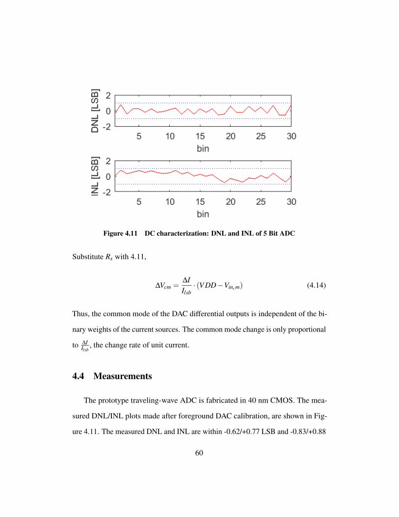
Figure 4.11 DC characterization: DNL and INL of 5 Bit ADC
Substitute Rs with 4.11,
∆Vcm =∆IIlsb· (V DD−Vincm) (4.14)
Thus, the common mode of the DAC differential outputs is independent of the bi-
nary weights of the current sources. The common mode change is only proportional
to ∆IIlsb
, the change rate of unit current.
4.4 Measurements
The prototype traveling-wave ADC is fabricated in 40 nm CMOS. The mea-
sured DNL/INL plots made after foreground DAC calibration, are shown in Fig-
ure 4.11. The measured DNL and INL are within -0.62/+0.77 LSB and -0.83/+0.88
60

Figure 4.12 Measured normalized spectrum for 4.24 MHz input sampled at 4 GS/s
LSB, respectively.
With single tone 4.24 MHz sinewave input, the ADC achieves 21.35 dB SNDR
(3.25 bit ENOB) and 30.18dB SFDR at a 4GS/s clock sampling rate, as shown in
Figure 4.12. With an increased sampling clock rate of 6 GS/s, and a single tone
6.36 MHz sinewave input, the ADC achieves 19.1 dB SNDR (2.88 bit ENOB) and
28.7 dB SFDR, as shown in Figure 4.13. The power consumption is 38.2 mW
(clock buffer 2.1 mW, comparator 8.7 mW, DAC 26 mW, others 1.35 mW), which
corresponds to 0.86 pJ/step FoM. The power breakdown is shown in Figure 4.14.
The on-chip LC transmission line is fabricated using top level thick metal M10 and
M9 as intersection. The capacitors are Metal-Insulator-Metal (MIM) structures.
Figure 4.15 shows one segment of transmission line between two active stages,
which consists of four differential LC structures. The active die area of traveling-
wave ADC is 0.65 mm2 and the die micrograph is shown in Figure 4.16.
61
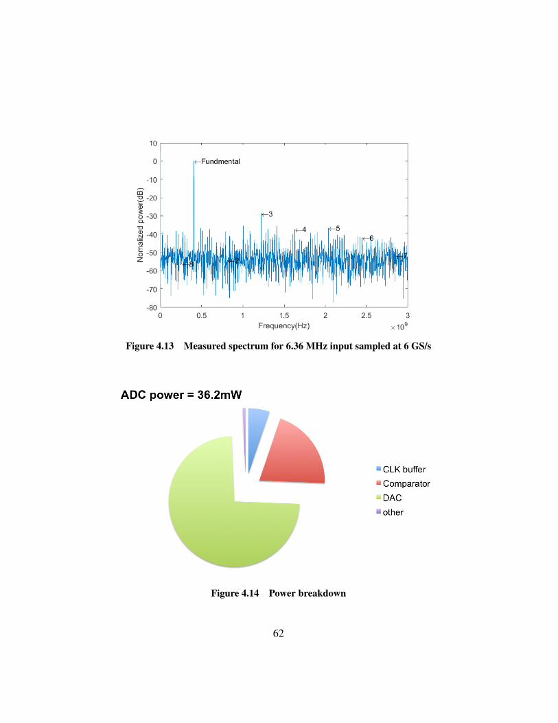
Figure 4.13 Measured spectrum for 6.36 MHz input sampled at 6 GS/s
Figure 4.14 Power breakdown
62
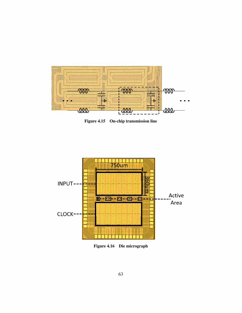
Figure 4.15 On-chip transmission line
Figure 4.16 Die micrograph
63
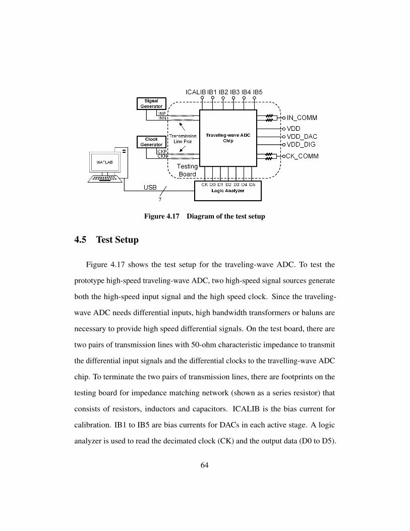
Figure 4.17 Diagram of the test setup
4.5 Test Setup
Figure 4.17 shows the test setup for the traveling-wave ADC. To test the
prototype high-speed traveling-wave ADC, two high-speed signal sources generate
both the high-speed input signal and the high speed clock. Since the traveling-
wave ADC needs differential inputs, high bandwidth transformers or baluns are
necessary to provide high speed differential signals. On the test board, there are
two pairs of transmission lines with 50-ohm characteristic impedance to transmit
the differential input signals and the differential clocks to the travelling-wave ADC
chip. To terminate the two pairs of transmission lines, there are footprints on the
testing board for impedance matching network (shown as a series resistor) that
consists of resistors, inductors and capacitors. ICALIB is the bias current for
calibration. IB1 to IB5 are bias currents for DACs in each active stage. A logic
analyzer is used to read the decimated clock (CK) and the output data (D0 to D5).
64
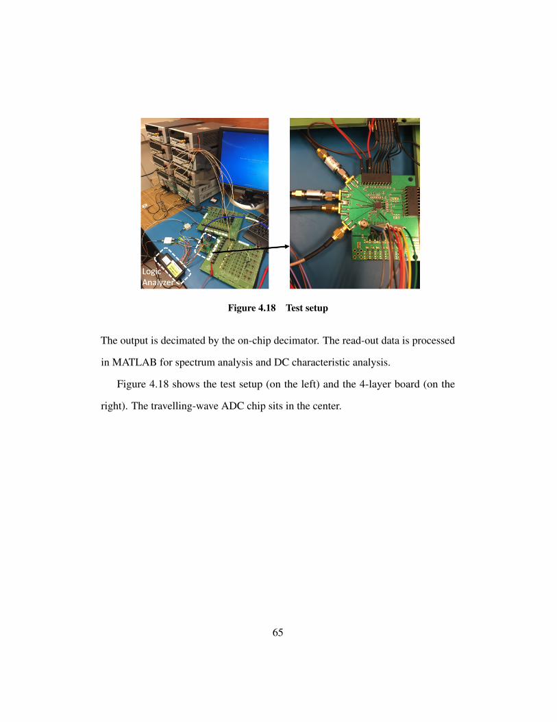
Figure 4.18 Test setup
The output is decimated by the on-chip decimator. The read-out data is processed
in MATLAB for spectrum analysis and DC characteristic analysis.
Figure 4.18 shows the test setup (on the left) and the 4-layer board (on the
right). The travelling-wave ADC chip sits in the center.
65
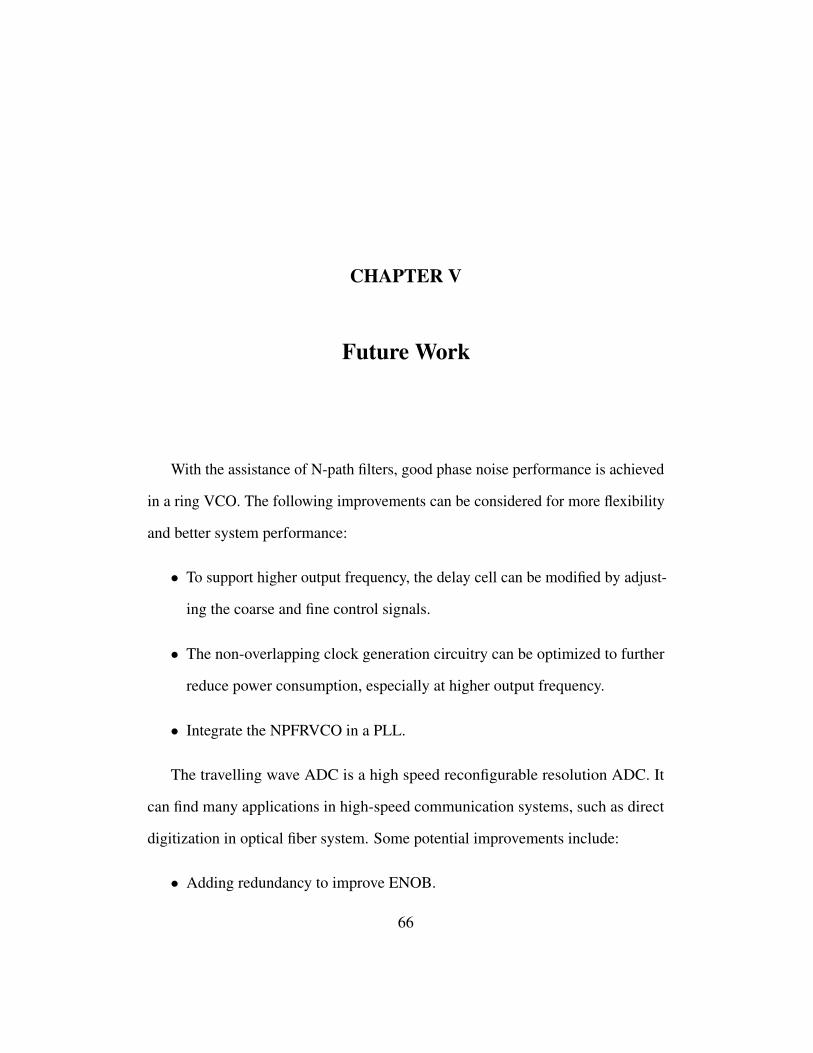
CHAPTER V
Future Work
With the assistance of N-path filters, good phase noise performance is achieved
in a ring VCO. The following improvements can be considered for more flexibility
and better system performance:
• To support higher output frequency, the delay cell can be modified by adjust-
ing the coarse and fine control signals.
• The non-overlapping clock generation circuitry can be optimized to further
reduce power consumption, especially at higher output frequency.
• Integrate the NPFRVCO in a PLL.
The travelling wave ADC is a high speed reconfigurable resolution ADC. It
can find many applications in high-speed communication systems, such as direct
digitization in optical fiber system. Some potential improvements include:
• Adding redundancy to improve ENOB.
66

• Use of a single clock phase so that the on-chip transmission line for trans-
mitting clock is not necessary.
• Characterization of magnetic pulling and signal coupling from transmission
line to low metals.
• Layout of circuitry underneath transmission line to save area.
67
CHAPTER VI
Conclusion
The prototype N-path filter enhanced voltage-controlled ring oscillator (NPFRVCO)
achieves a measured phase noise of -110 dBc/Hz at a 1 MHz offset frequency for
an oscillation frequency of 1.0 GHz. The self-clocked N-path filter reduces the
phase noise by 10 dB and 28 dB for 1.0 GHz and 300 MHz oscillation frequencies,
respectively. Implemented in 65 nm CMOS, the NPFRVCO occupies a die area
of 0.015 mm2 and consumes 4.7 mW from 1.2 V power supply when operating at
1.0 GHz. The NPFRVCO has a measured frequency tuning range from 300 MHz
to 1.6 GHz and achieves a FoM of 163 dB at 1 MHz offset.
This research developed and demonstrated new techniques that enable energy
efficient, very-high-speed, moderate resolution analog-to-digital conversion. On-
chip transmission lines provide sufficient delay between decision stages, avoiding
the need for power hungry high-bandwidth track-and hold amplifiers. The feedfor-
ward settings of DACs further relax the timing constraints of delay between stages.
Current summing of the current steering DAC requires no high speed digital logic
68
in the critical path. The scheme combines the efficiency of the SAR technique
with the throughput of flash. With a energy efficiency of 0.895 pJ per conversion
bit, this very-high-speed ADC will facilitate ADC-based wireline links, optical
communication system and high bandwidth wireless communication systems such
as next generation cellular.
The key contributions of this research are summarized as follows:
• A novel scheme to reduce phase noise of ring VCO using N-path filter.
• A completely new ADC scheme based on a traveling wave structure.
• Compact on-chip transmission line design and characterization.
• Design of a prototype power-efficient very-high-speed ADC.
69

BIBLIOGRAPHY
70
BIBLIOGRAPHY
[1] [Online]. Available: http://www.nextbigfuture.com/2016/06/qualcomm-demos-5g-prototype-for.html
[2] [Online]. Available: http://bwrcs.eecs.berkeley.edu/Classes/icdesign/ee290cs11/lectures/Lecture01 Intro 2up.pdf
[3] V. Stojanovic and M. Horowitz, “Modeling and analysis of high-speed links,”in Proceedings of the IEEE 2003 Custom Integrated Circuits Conference,2003. IEEE, 2003, pp. 589–594.
[4] [Online]. Available: https://telecomstudy18.blogspot.com/2014/07/lte-resource-block-flexible-bandwidth.html
[5] A. Hajimiri and T. H. Lee, The design of low noise oscillators. SpringerScience & Business Media, 1999.
[6] W. A. Kester, Data conversion handbook. Newnes, 2005.
[7] [Online]. Available: http://cp.literature.agilent.com/litweb/pdf/5989-7273EN.pdf
[8] D. B. Alan, “Thermionic valve circuits,” Dec. 16 1941, US Patent 2,266,154.
[9] [Online]. Available: http://www.ctia.org/your-wireless-life/how-wireless-works/annual-wireless-industry-survey
[10] [Online]. Available: https://standards.ieee.org/about/get/802/802.11.html
[11] [Online]. Available: http://www.3gpp.org/specifications/releases/72-release-8
[12] A. A. Abidi, “Phase noise and jitter in cmos ring oscillators,” IEEE Journalof Solid-State Circuits, vol. 41, no. 8, pp. 1803–1816, 2006.
71

[13] B. Zhang, A. Nazemi, A. Garg, N. Kocaman, M. R. Ahmadi, M. Khanpour,H. Zhang, J. Cao, and A. Momtaz, “A 195mw/55mw dual-path receiver afefor multistandard 8.5-to-11.5 gb/s serial links in 40nm cmos,” in 2013 IEEEInternational Solid-State Circuits Conference Digest of Technical Papers.IEEE, 2013, pp. 34–35.
[14] S. Le Tual, P. N. Singh, C. Curis, and P. Dautriche, “22.3 a 20ghz-bw 6b10gs/s 32mw time-interleaved sar adc with master t&h in 28nm utbb fdsoitechnology,” in 2014 IEEE International Solid-State Circuits ConferenceDigest of Technical Papers (ISSCC). IEEE, 2014, pp. 382–383.
[15] C.-C. Liu, C.-H. Kuo, and Y.-Z. Lin, “A 10 bit 320 ms/s low-cost sar adcfor ieee 802.11 ac applications in 20 nm cmos,” IEEE Journal of Solid-StateCircuits, vol. 50, no. 11, pp. 2645–2654, 2015.
[16] B. E. Boser and B. A. Wooley, “The design of sigma-delta modulation analog-to-digital converters,” IEEE Journal of solid-state circuits, vol. 23, no. 6, pp.1298–1308, 1988.
[17] G. Van der Plas, S. Decoutere, and S. Donnay, “A 0.16 pj/conversion-step 2.5mw 1.25 gs/s 4b adc in a 90nm digital cmos process,” in IEEE InternationalSolid-State Circuits Conference, 2006. ISSCC 2006. Digest of TechnicalPapers. IEEE, 2006, p. 2310.
[18] S. Park, Y. Palaskas, and M. P. Flynn, “A 4gs/s 4b flash adc in 0.18/spl mu/mcmos,” in 2006 IEEE International Solid State Circuits Conference-Digest ofTechnical Papers. IEEE, 2006, pp. 2330–2339.
[19] Y. Dong, J. Zhao, W. Yang, T. Caldwell, H. Shibata, R. Schreier, Q. Meng,J. Silva, D. Paterson, and J. Gealow, “15.5 a 930mw 69db-dr 465mhz-bw ct1-2 mash adc in 28nm cmos,” in 2016 IEEE International Solid-State CircuitsConference (ISSCC). IEEE, 2016, pp. 278–279.
[20] V. Srinivasan, V. Wang, P. Satarzadeh, B. Haroun, and M. Corsi, “A 20mw61db sndr (60mhz bw) 1b 3 rd-order continuous-time delta-sigma modulatorclocked at 6ghz in 45nm cmos,” in 2012 IEEE International Solid-StateCircuits Conference. IEEE, 2012, pp. 158–160.
[21] B. Setterberg, K. Poulton, S. Ray, D. J. Huber, V. Abramzon, G. Steinbach,J. P. Keane, B. Wuppermann, M. Clayson, M. Martin et al., “26.3 a 14b 2.5
72
gs/s 8-way-interleaved pipelined adc with background calibration and digitaldynamic linearity correction,” 2013.
[22] J. Wu, A. Chou, C.-H. Yang, Y. Ding, Y.-J. Ko, S.-T. Lin, W. Liu, C.-M.Hsiao, M.-H. Hsieh, C.-C. Huang et al., “A 5.4 gs/s 12b 500mw pipeline adcin 28nm cmos,” in 2013 Symposium on VLSI Circuits, 2013.
[23] J. Wu, A. Chou, T. Li, R. Wu, T. Wang, G. Cusmai, S.-T. Lin, C.-H. Yang,G. Unruh, S. R. Dommaraju et al., “27.6 a 4gs/s 13b pipelined adc withcapacitor and amplifier sharing in 16nm cmos,” in 2016 IEEE InternationalSolid-State Circuits Conference (ISSCC). IEEE, 2016, pp. 466–467.
[24] M. Brandolini, Y. Shin, K. Raviprakash, T. Wang, R. Wu, H. M. Geddada,Y.-J. Ko, Y. Ding, C.-S. Huang, W.-T. Shin et al., “26.6 a 5gs/s 150mw 10bsha-less pipelined/sar hybrid adc in 28nm cmos,” in 2015 IEEE InternationalSolid-State Circuits Conference-(ISSCC) Digest of Technical Papers. IEEE,2015, pp. 1–3.
[25] B. Murmann. Adc survey. [Online]. Available: https://web.stanford.edu/∼murmann/adcsurvey.html
[26] E. J. Pankratz and E. Sanchez-Sinencio, “Multiloop high-power-supply-rejection quadrature ring oscillator,” IEEE Journal of Solid-State Circuits,vol. 47, no. 9, pp. 2033–2048, 2012.
[27] J. Borremans, J. Ryckaert, C. Desset, M. Kuijk, P. Wambacq, and J. Craninckx,“A low-complexity, low-phase-noise, low-voltage phase-aligned ring oscillatorin 90 nm digital cmos,” IEEE journal of solid-state circuits, vol. 44, no. 7, pp.1942–1949, 2009.
[28] A. Ismail and A. A. Abidi, “Cmos differential lc oscillator with suppressedup-converted flicker noise,” ISSCC Dig. Tech. Papers, pp. 98–99, 2003.
[29] L. Franks and I. Sandberg, “An alternative approach to the realization ofnetwork transfer functions: The n-path filter,” Bell System Technical Journal,vol. 39, no. 5, pp. 1321–1350, 1960.
[30] A. Ghaffari, E. A. Klumperink, M. C. Soer, and B. Nauta, “Tunable high-q n-path band-pass filters: Modeling and verification,” IEEE journal of solid-statecircuits, vol. 46, no. 5, pp. 998–1010, 2011.
73

[31] [Online]. Available: http://cp.literature.agilent.com/litweb/pdf/5989-8371EN.pdf
[32] [Online]. Available: http://cp.literature.agilent.com/litweb/pdf/5989-7273EN.pdf
[33] A. Varzaghani, A. Kasapi, D. N. Loizos, S.-H. Paik, and S. Verma, “A 10.3-gs/s, 6-bit flash adc for 10g ethernet applications,” IEEE Journal of Solid-StateCircuits, vol. 48, no. 12, pp. 3038–3048, 2013.
[34] B. Analui and A. Hajimiri, “Statistical analysis of integrated passive delaylines,” in Proceedings of the IEEE 2003 Custom Integrated Circuits Confer-ence, 2003. IEEE, 2003, pp. 107–110.
[35] J. Montanaro, R. T. Witek, K. Anne, A. J. Black, E. M. Cooper, D. W.Dobberpuhl, P. M. Donahue, J. Eno, W. Hoeppner, D. Kruckemyer et al., “A160-mhz, 32-b, 0.5-w cmos risc microprocessor,” IEEE Journal of Solid-StateCircuits, vol. 31, no. 11, pp. 1703–1714, 1996.
[36] G. Mitteregger, C. Ebner, S. Mechnig, T. Blon, C. Holuigue, and E. Romani,“A 20-mw 640-mhz cmos continuous-time adc with 20-mhz signal bandwidth,80-db dynamic range and 12-bit enob,” IEEE journal of solid-state circuits,vol. 41, no. 12, pp. 2641–2649, 2006.
74