Embed Size (px)
Citation preview

7/27/2019 Buck and Boost Converters With Transmission Lines
http://slidepdf.com/reader/full/buck-and-boost-converters-with-transmission-lines 1/8
IEEE TRANSACTIONS ON POWER ELECTRONICS, VOL. 27, NO. 9, SEPTEMBER 2012 4013
Buck and Boost Converters With Transmission LinesSverker Sander, Member, IEEE
Abstract —The switch mode power conversion circuits buck,
boost, and buck–boost incorporate a power inductor as an en-ergy storage device. If the power inductor in these fundamentalcircuits is replaced with a transmission line, new power conversioncircuits will emerge. By introducing microwave properties, suchas propagation delay and characteristic impedance, new functionsmay be feasible in the area of power conversion. Examples of suchfunctions could be inverting and noninverting voltage polarity abil-ities or circuits, which share switch components between multipleoutput voltages reducing the number of semiconductors needed.Alternatively, the buck–boost power converter circuit may giverise to new high-efficiency radio circuits in the area of microwavetechnology.
Index Terms —AC-DC power converters, dc–dc power convert-ers, radio, radio frequency (RF), transmission line (TL).
I. INTRODUCTION
POWER conversion using transmission lines (TLs) as ameans of dc–dc, ac–dc, and dc–ac conversion has been
studied [1]–[7] as an alternative to the use of power inductors.The electrical circuits evaluated were mainly amplifier circuitsadapted to perform power conversion. An energy accumulationand discharge cycle synchronous with the TL’s self-resonancefrequency was completed. The TL or wave propagation mediumcould be a coaxial cable, a printed circuit board microstrip, orbuilt using multiple lumped inductors and capacitors forming
an LC network [8].In this paper, energy accumulation in TLs with frequencies an
order of magnitude lower than their self-resonance frequency isdiscussed. This mode of operation may result in high-efficiencypower conversion, without using any amplifier variants, but in-stead derived directly from the original buck, boost, and buck–boost circuits.
II. SUBSAMPLING
A. General
The low-frequency properties of a TL are studied by plotting
voltage and current waves against time, when a dc voltage sourceis applied momentarily to its input, by means of an ideal switch.
Fig. 1 shows a time-space diagram where the voltage (hatchedarea) and current (cross-hatched area) along the length of theTL are plotted horizontally on the vertical time axis at differenttime instances. The reference lines, ending with black dots,
Manuscript received October 5, 2011; revised December 13, 2011; acceptedJanuary 31, 2012. Date of current version May 15, 2012. Recommended forpublication by Associate Editor D. Maksimovic.
The author is with Ericsson Power Solutions, SE-417 56 Gothenburg,Sweden(e-mail: [email protected]).
Digital Object Identifier 10.1109/TPEL.2012.2188044
Fig. 1. Time-space diagram of a short-circuited transmission line (TL), mo-mentarilyconnected to a low impedancedc sourceV INDC , bymeans ofan idealswitch S.
represent zero voltage and zero current in the vertical direction.The propagation delay, i.e., the time taken for a wave to travelfrom the TL input to the TL output, is denoted here as td (in
seconds).
0885-8993/$31.00 © 2012 IEEE

7/27/2019 Buck and Boost Converters With Transmission Lines
http://slidepdf.com/reader/full/buck-and-boost-converters-with-transmission-lines 2/8
4014 IEEE TRANSACTIONS ON POWER ELECTRONICS, VOL. 27, NO. 9, SEPTEMBER 2012
B. Time Instance t = 0
Switch S is closed at time instance t= 0, thereby connectinga dc input voltage V INDC to the TL. The initial current step Δi1into the TL will be determined by the characteristic impedanceZ 0 and the input voltage vINTL , according to
Δi1 =
vINTL
Z 0 =
V INDC
Z 0 . (1)
For example, the dc input voltage is V INDC = 10 V, and thecharacteristic impedance Z 0 = 10 Ω. A positive 1 A currentwave, and a positive 10 V voltage wave, will consequently startto propagate into the TL.
C. Time Instance t = td
The waves reach the output end of the TL at time instancet = t d . According to basic microwave theory, the waves aretransmitted to, or reflected within, the load impedance depend-ing on the reflection coefficient Γ [11]. The load impedance Z L
connected to the output end of the TL is (see Fig. 1) a perfectshort circuit, thus giving Z L a value of 0 Ω
ΓOUT =Z L − Z 0
Z L + Z 0. (2)
Inserting Z L = 0 Ω and Z 0 = 10 Ω into (2) yields ΓOUT =−1.The voltage wave will consequently be reflected with invertedpolarity, while the current wave will be reflected with unchangedpolarity. The voltage along the TL will now start to fall back tozero volts (half completed at time instance t = 1.5td ) since thereflected negative voltage wave propagating toward the TL inputwill be superimposed on its positive voltage tail. The reflectedcurrent wave will retain its positive polarity, thus creating an
increase in current amplitude to 2 A (half completed at timeinstance t = 1.5td).
D. Time Instance t = 2td
At time instance t = 2td the current and voltage waves willreach the TL input. Frequency f 5 corresponds to the fifth har-monic of the square wave-shaped waveform present at the TLinput, having a fundamental frequency of f 1 = 1/2td . The dcvoltage source V INDC in the applications discussed in this pa-per represents an upstream dc–dc converter or a native powerconverter input filter. In both the cases (assuming that frequencyf 5 is higher than the dc–dc converter’s control bandwidth), the
output impedanceZ G of those two circuits is mainly determinedby the LC filter’s capacitors. Typically, several capacitors of thesame or mixed types are parallel-coupled to give low impedanceover a wide frequency band. These capacitors may for examplebe of electrolytic, ceramic or tantalum types. Generally, theseparallel-coupled capacitors will have an absolute impedance inthe milliohm range
|Z G | ≈ X C +X ESL + ESR =1
2πf 5C + 2πf 5ESL+ ESR.
(3)The absolute value of the Z G impedance is calculated using thefollowing typical figures corresponding to 10-parallel-coupled
ceramic capacitors where C = 22 μF, ESL = 0.5 nH, ESR =
Fig. 2. Circuit diagram forthe voltage-step responseanalysis of a transmissionline TL and an inductor L.
3 mΩ
, and f 5=
5/2td=
5 MHz. Inserting these figures into (3)gives |Z G | = 20 mΩ. The reflection coefficient of the TL inputΓIN can now be calculated by inserting (3) into (4). The phase isneglected in (3) and the complex variable ΓIN has no imaginarypart in this example
ΓIN =Z G − Z 0
Z G + Z 0. (4)
Inserting the figures gives ΓIN = (0.02 − 10) / (0.02 + 10) =−0.996. As noted, the value ΓIN is close to −1, causing a sec-ond reflection of the voltage and current waves in the mannerdescribed at time instance t = td . The voltage wave will be re-flected with inverted polarity, fitting into the positive dc voltage
V INDC present at the TL input.The current wave will be reflected a second time with un-
changed polarity, thus creating an increase in current amplitudeto 3 A (half completed at time instance t = 2.5td). This is animprint of the initial current step (1), but with doubled amplitude
Δi2 =2vINTL
Z 0=2V INDC
Z 0. (5)
Assuming the TL to be lossless, the reflections described earlierat t = td and t = 2td will continue to take place with td timeintervals.
E. Comparison of TL and Inductor Input CurrentsThe operation described earlier, i.e., the momentary connec-
tion of a low impedance dc source to a TL short-circuited at itsfar end, is now analyzed a second time but with emphasis on theinput current, rather than observing the inherent waves propa-gating inside the TL. Fig. 2 shows two circuits, the first incorpo-rating a TL and the second an inductor L which are comparedwith respect to input currents. Switches STL and SL are closedat t = 0, thus connecting the dc input voltage source V INDC tothe TL, and inductor L, respectively, as seen in Fig. 3(a).
By continuously plotting the current at the leftmost positionalong the TL in Fig. 1, a staircase shaped slope is obtained
for iTL as presented in Fig. 3(b) (solid line). The current iTL
7/27/2019 Buck and Boost Converters With Transmission Lines
http://slidepdf.com/reader/full/buck-and-boost-converters-with-transmission-lines 3/8
SANDER: BUCK AND BOOST CONVERTERS WITH TRANSMISSION LINES 4015
Fig. 3. Accumulation of energy by using subsampling mode. (a) Switch statefor switches STL (solid line) and SL (dotted line). (b) Input current into TLiTL (solid line) and inductor iL (dotted line).
increases in amplitude at discrete time points distributed withintervals of 2td length, while the inductor current iL (dottedline) increases continuously.
From a low frequency perspective, i.e., during a number of reflections, the TL can be modeled as an inductor L. The induc-
tance value of such model can be calculated using the formula
L= d · l (6)
where d is the TL length in meters (m) and l is the inductanceper meter (H/m). If the TL is designed with multiple lumpedinductors and capacitors forming an LC network, the inductancevalue of such model can be calculated using the formula
L= N · L (7)
where N is the integer number of LC elements and L is theinductance value of each LC element.
The operation of accumulating energy in (or discharging en-
ergy from) a TL over a time interval exceeding 2td in length isreferred to, in this paper, as subsampling.
III. OVERSAMPLING
The option of accumulating and discharging energy syn-chronous to one of the TL’s self-resonance frequencies is calledoversampling mode in this paper. To visualize this mode of op-eration, a second switch SB is connected to an arbitrary loadX LD as shown in Fig. 4.
Energy is accumulated in the TL by briefly turning ON switchSA as shown in Fig. 5(a). A current and a voltage wave will con-sequently start to propagate into the TL. At time instance t = t d ,
the waves are totally reflected in the TL’s short-circuited output
Fig. 4. Circuit diagram for the description of energy accumulation and dis-charge into a load synchronous to the TL’s self-resonance frequency.
Fig. 5. Energy accumulation and discharge into the substantially capacitiveload X LD by using oversampling mode. (a) Switch state for switches SA (solidline) and SB (dotted line). (b) Current through switch SA iSA (solid line) andswitch SB iSB (dotted line).
end. At time instance t = 2td , the current and voltage waves willreach the TL input and switch SB is turned ON, thus partiallyor totally discharging the energy into the load X LD . Switch SAmust be turned OFF before time instance t= 2td to avoid crossconduction with switch SB . The energy accumulation interval
T AccOVS is consequently limited to less than 2td in length asshown in Fig. 5(b).
Voltage conversion of the input voltage V INDC to a differ-ent output voltage vOUT cannot be performed by controllingthe current fluctuation with the low-frequency inductance L asdepicted in Fig 3. On the contrary, the input to output voltageconversion in oversampling mode is not effectuated until thewaves reach a mismatched load X LD (alternatively, no voltageconversion will occur at all if load X LD is perfectly matched toZ 0). The current fluctuation in oversampling mode is controlledby producing numerous reflections back and forth between theTL’s input and output ends, generating losses in the TL’s resis-
tive elements.
7/27/2019 Buck and Boost Converters With Transmission Lines
http://slidepdf.com/reader/full/buck-and-boost-converters-with-transmission-lines 4/8
4016 IEEE TRANSACTIONS ON POWER ELECTRONICS, VOL. 27, NO. 9, SEPTEMBER 2012
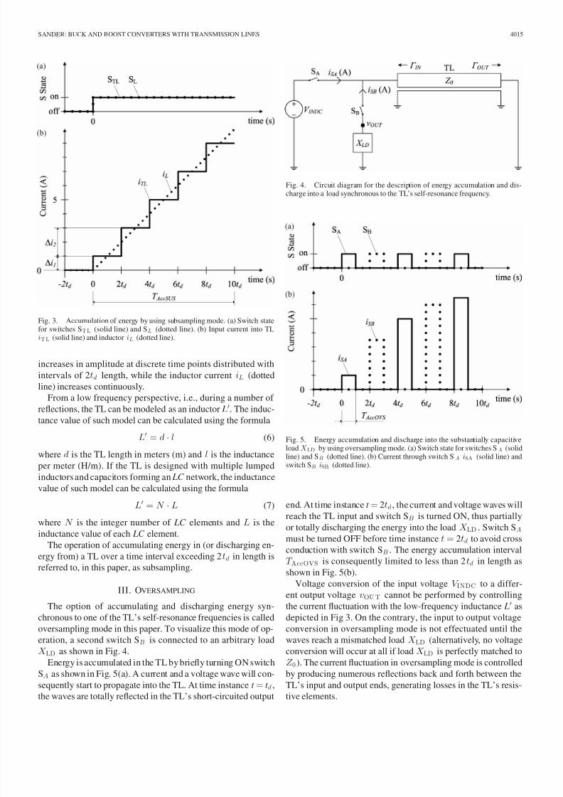
Fig. 6. Accumulation of energy using mixed sub- and oversampling mode.(a) Switch state for switches STL (solid line) and SL (dotted line). (b) Inputcurrent into TL iTL (solid line) and inductor L iL (dotted line).
TABLE ICOMPARISON OF OPERATION MODES
IV. MIXED SUB- AND OVERSAMPLING
The option of operating switch STL synchronous with oneof the TL’s self-resonance frequencies, without the transitionsfrom TL energy accumulation to energy discharge or vice versa,is called mixed sub- and oversampling mode. The switch stateand current waveforms in Fig. 6 again refer to the circuit dia-gram presented in Fig. 2. One of the TL’s resonance frequenciesis excited, but contrary to oversampling mode, the resonance
frequency is used for energy accumulation during several reflec-tions, again controlling the current fluctuation by low-frequencyinductance L.
To summarize the three modes of operation described in Sec-tions II–IV, a comparison of the energy accumulation intervallengths (T AccSUS , T AccOVS, and T AccMSO in Figs. 3, 5, and 6,respectively) is provided in Table I.
V. VARIANT FORMATION
New power conversion circuits can be derived depending onthe mode of operation. To distinguish circuits using a wavepropagation medium from their inductor-based counterparts,
the prefix prime is added before the circuit name, e.g., buck
becomes prime buck. Fig. 7 compiles variant formation in se-lection, where each column shows buck (U), boost (O), andbuck–boost (B) derived circuits, respectively. Four modes of operation are listed vertically in the following order: subsam-pling (s), oversampling (o), alternating sub- and oversampling(a), and mixed sub- and oversampling (m). The capital and low-ercase letters in brackets are used to form reference numbersfor the different prime-power conversion circuits in Fig. 7. Anumerical series is assigned to all circuits sharing the sametopology (U, O, or B) and mode (s, o, a, or m) thus substantiallyreflecting the circuit’s complexity.
Power conversion is possible using subsampling solely, butvoltage and current waves will reside in the TL without intro-ducing any new circuit options or features [9]. The number of circuits using subsampling is therefore just three (Us1, Os1, andBs1).
When using oversampling, new circuit formations are possi-ble. The drawback of using oversampling mode solely is thatvoltage conversion is effectuated in the mismatched load, pro-
ducing numerous reflections that generate losses as describedin Section III. However, features created in this mode reap-pear in mixed sub- and oversampling modes and in these casesare feasible with high power conversion efficiency. As an ex-ample, the short-circuited end of the TL in Bo1 can be leftopen, thus creating circuit Bo2. The Bo1 circuit will invert theinput dc voltage polarity, in the same manner as in the buck–boost converter. However, because the voltage waves will bereflected with unchanged polarity in an open termination, Bo2will provide noninverting power conversion. This feature can befurther controlled by adding a third switch element, located atthe TL’s far end, as shown in circuit Bo5. The output voltage
can consequently be controlled to obtain dc–ac, ac–dc, or ac–acpower conversion. Oversampling also introduces the possibilityof sharing switch elements between multiple output voltages(Uo3, Oo2, Bo3, and Bo4). Two independently controlled out-put voltages, which are higher than the input voltage, normallyrequire two boost converters incorporating a total of four semi-conductors (two switches and two diodes). Circuit Oo2 can per-form the same task with just three semiconductors since the lowside switch (and common TL) are used by both output voltages.
The third mode is obtained by sequentially alternating sub-and oversampling modes. As an example, energy can be ac-cumulated in the Ba1 circuit TL over a long (e.g., T = 10td)subsampling interval, directly followed by a voltage wave po-
larity change effected by opening the low side switch brieflyduring an oversampling interval (T = 2td), followed in turn byan energy discharge into the output capacitor during a secondsubsampling interval (e.g., T = 20td ). This type of operationmay be used in, for example, ac–dc conversion, where the po-larity changing feature rectifies the input ac voltage. CircuitsOa1, Ba2, Ba3, and Ba4 represent prime boost and prime buck–boost pulsed amplifier circuits. The output impedance of thesecircuits can be determined by the characteristic impedance of the TL by omitting the original converter’s output capacitor, andcan therefore be matched to defined load impedances. A detaileddescription of circuit Oa1 can be found in Section VI. The low
side switch may also be used to generate radio carriers (Ba5,

7/27/2019 Buck and Boost Converters With Transmission Lines
http://slidepdf.com/reader/full/buck-and-boost-converters-with-transmission-lines 5/8
SANDER: BUCK AND BOOST CONVERTERS WITH TRANSMISSION LINES 4017
Fig. 7. Variant formation derived from buck, boost, and buck–boost circuits.
TABLE IICOMPONENTS FOR PULSED AMPLIFIER
Ba6), thus creating a simple yet highly efficient circuit forming acomplete pulsed radio transmitter [9]. For this reason, the loadsare represented by antennae symbols.
The fourth mode is obtained by simultaneously mixing sub-
and oversampling modes as previously described in SectionIV [10]. A detailed description of circuit Om2 can be found inSection VII.
The circuit types listed under alternating sub- and oversam-pling mode and mixed sub- and oversampling mode can be usedto create efficient power converters and some of them may findpractical applications.
Fig. 7 shows a selection of prime-power conversion circuits.The list canbe expanded by introducing multiple TLs (i.e.,creat-ing prime single-ended primary-inductance converter or primeCuk circuits) or isolated variants can be created by replacingeach inductor in an LC network TL with a miniature core trans-
former, or using coreless microstrip transformers [6].
VI. PULSED AMPLIFIER EXAMPLE
A. Simulation Verification
The prime boost circuit Oa1, presented in Fig. 7, is simulatedin this section by means of a lumped TL designed using 40 dis-crete LC elements. The main components are listed in Table II.Inductor models include dc resistance and parallel stray ca-pacitance derived from the inductor self-resonance frequency.Capacitor models include equivalent series inductance (ESL)and equivalent series resistance (ESR).
The circuit, detailed in Fig. 8, is operated in alternating sub-and oversampling mode. This circuit can be used in amplifierapplications where the load impedance R is defined and givingefficiencies close to conventional power converters. The circuitgenerates a pulsed output voltage that is, for example, applicablein radar transmitters where RF signals are amplitude-modulatedaccording to the system’s pulse repetition frequency (PRF). Acontinuousmodulated output voltage can be achieved by parallelcoupling of multiple Ba2 circuits, shown in Fig. 7, as in a con-ventional multiphase power converter. A continuous modulatedoutput voltage is, for example, applicable in envelope trackingradio transmitters where RF signals are amplitude-modulated to
carry information.
7/27/2019 Buck and Boost Converters With Transmission Lines
http://slidepdf.com/reader/full/buck-and-boost-converters-with-transmission-lines 6/8
4018 IEEE TRANSACTIONS ON POWER ELECTRONICS, VOL. 27, NO. 9, SEPTEMBER 2012
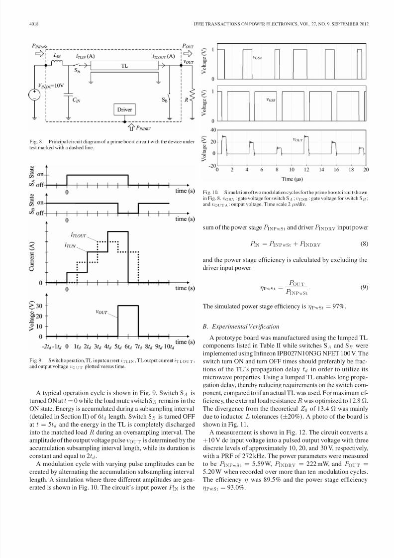
Fig. 8. Principal circuit diagram of a prime boost circuit with the device undertest marked with a dashed line.
Fig. 9. Switchoperation,TL inputcurrent iTLIN , TL output current iTLOUT ,and output voltage vOUT plotted versus time.
A typical operation cycle is shown in Fig. 9. Switch SA isturned ON at t= 0 while the load mute switch SB remains in theON state. Energy is accumulated during a subsampling interval(detailed in Section II) of 6td length. Switch SB is turned OFFat t = 5td and the energy in the TL is completely dischargedinto the matched load R during an oversampling interval. Theamplitude of the output voltage pulse vOUT is determined by theaccumulation subsampling interval length, while its duration isconstant and equal to 2td .
A modulation cycle with varying pulse amplitudes can becreated by alternating the accumulation subsampling intervallength. A simulation where three different amplitudes are gen-
erated is shown in Fig. 10. The circuit’s input power P IN is the
Fig. 10. Simulation oftwo modulation cycles forthe prime boostcircuitshownin Fig. 8. vGSA : gate voltage for switch SA ; vGSB : gate voltage for switch SB ;and vOUTA : output voltage. Time scale 2 μs/div.
sum of the power stageP INPwSt and driverP INDRV input power
P IN = P INPwSt + P INDRV (8)
and the power stage efficiency is calculated by excluding thedriver input power
ηPwSt =P OUT
P INPwSt. (9)
The simulated power stage efficiency is ηPwSt = 97%.
B. Experimental Verification
A prototype board was manufactured using the lumped TLcomponents listed in Table II while switches SA and SB wereimplemented using Infineon IPB027N10N3G NFET 100 V. Theswitch turn ON and turn OFF times should preferably be frac-tions of the TL’s propagation delay td in order to utilize itsmicrowave properties. Using a lumped TL enables long propa-gation delay, thereby reducing requirements on the switch com-
ponent, compared to if an actual TL was used. For maximum ef-ficiency, the external load resistanceR was optimized to 12.8Ω.The divergence from the theoretical Z 0 of 13.4 Ω was mainlydue to inductor L tolerances (±20%). A photo of the board isshown in Fig. 11.
A measurement is shown in Fig. 12. The circuit converts a+10 V dc input voltage into a pulsed output voltage with threediscrete levels of approximately 10, 20, and 30 V, respectively,with a PRF of 272 kHz. The power parameters were measuredto be P INPwSt = 5.59 W, P INDRV = 222 mW, and P OUT =
5.20 W when recorded over more than ten modulation cycles.The efficiency η was 89.5% and the power stage efficiency
ηPwSt = 93.0%.
7/27/2019 Buck and Boost Converters With Transmission Lines
http://slidepdf.com/reader/full/buck-and-boost-converters-with-transmission-lines 7/8
SANDER: BUCK AND BOOST CONVERTERS WITH TRANSMISSION LINES 4019
Fig. 11. Photo of the prime boost prototype board. The lumped TL is visibleon the right-hand side, while the drivers and switches, SA and SB , are locatedon each side of the lumped TL. The board measures 12 cm × 18cm.
Fig. 12. (a) Measured gate-source voltage for switch SA . (vGSA : 10 V/div).(b) Gate-source voltage for switch SB . (vGSB : 10 V/div.) (c) Output voltagevOUT 20 V/div with a time scale of 2μs/div. One modulation cycle, includingthree discrete voltage levels, is repeated twice. Note that the output voltagepulses increase in amplitude when preceded by longer energy accumulationsubsampling intervals.
VII. DC–DC CONVERTER EXAMPLE
The prime boost circuit Om2 presented in Fig. 7 is simulatedhere with thecomponents listedin Table II. However, thenumberof LC elements N is increased to 50, producing a propagationdelay of 374 ns. The circuit is operated in mixed sub- andoversampling mode to perform dc–dc conversion.
Achieving two individually controlled stepped up output volt-ages normally requires two boost converters, including twoswitches and two rectifiers, giving a total of four semiconduc-tors. In the simulation, the same function is performed using
only three semiconductors. The prime boost principal circuitdiagram is shown in Fig. 13.
Each voltage output (V OUTA , V OUTB ) has its own dedicatedsynchronous rectifier (SA , SB ), but both output voltages shareone common low side switch SC and TL. Note that this type of circuit will be unable to operate if switches SA and SB are de-signed using switches with parallel body diodes, such as FETs.The load resistors RA and RB are of equal value and set to 20 Ωeach.
The start up operation cycle is shown in Fig. 14. Each outputvoltage has a dedicated time slot (marked with digits 1 and 2 inFig. 14) where the common low side switch SC , and the com-
mon TL, can be used independently for energy accumulation.
Fig. 13. Principal circuit diagram of a prime boost converter with two indi-vidually controlled output voltages.
Fig. 14. Simulated start up sequence of prime boost circuit shown in Fig. 13.vGSC : gate voltage for switch SC ; vGSA : gate voltage for switch SA ; vGSB :gate voltage for switch SB ; iSC : current in switch SC ; vOUTA : output voltageA; and vOUTB output voltage B. Time scale 1 μs/div. M B = 4.
Note the linearly increasing peaks of the iSC current waveformreflecting the TL’s low-frequency inductive properties. This en-ables operation of circuit Om2 with a power stage efficiencyclose to a boost converter’s power stage efficiency (not possiblewith circuit Oo2 operated in oversampling mode).
The simulation shown in Fig. 14 was run until a steady state
was detected and the dc output voltages were then recorded.
7/27/2019 Buck and Boost Converters With Transmission Lines
http://slidepdf.com/reader/full/buck-and-boost-converters-with-transmission-lines 8/8
4020 IEEE TRANSACTIONS ON POWER ELECTRONICS, VOL. 27, NO. 9, SEPTEMBER 2012
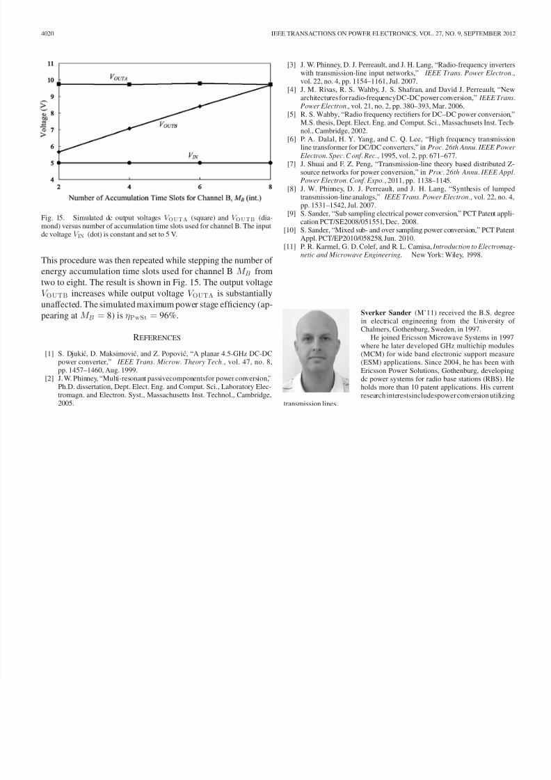
Fig. 15. Simulated dc output voltages V OUTA (square) and V OUTB (dia-mond) versus number of accumulation time slots used for channel B. The inputdc voltage V IN (dot) is constant and set to 5 V.
This procedure was then repeated while stepping the number of
energy accumulation time slots used for channel B M B fromtwo to eight. The result is shown in Fig. 15. The output voltageV OUTB increases while output voltage V OUTA is substantiallyunaffected. The simulated maximum power stage efficiency (ap-pearing at M B = 8) is ηPwSt = 96%.
REFERENCES
[1] S. Djukic, D. Maksimovic, and Z. Popovic, “A planar 4.5-GHz DC-DCpower converter,” IEEE Trans. Microw. Theory Tech., vol. 47, no. 8,pp. 1457–1460, Aug. 1999.
[2] J. W. Phinney, “Multi-resonant passivecomponentsfor power conversion,”Ph.D. dissertation, Dept. Elect. Eng. and Comput. Sci., Laboratory Elec-tromagn. and Electron. Syst., Massachusetts Inst. Technol., Cambridge,2005.
[3] J. W. Phinney, D. J. Perreault, and J. H. Lang, “Radio-frequency inverterswith transmission-line input networks,” IEEE Trans. Power Electron.,vol. 22, no. 4, pp. 1154–1161, Jul. 2007.
[4] J. M. Rivas, R. S. Wahby, J. S. Shafran, and David J. Perreault, “Newarchitectures for radio-frequencyDC-DC power conversion,” IEEE Trans. Power Electron., vol. 21, no. 2, pp. 380–393, Mar. 2006.
[5] R. S. Wahby, “Radio frequency rectifiers for DC–DC power conversion,”M.S. thesis, Dept. Elect. Eng. and Comput. Sci., Massachusets Inst. Tech-nol., Cambridge, 2002.
[6] P. A. Dalal, H. Y. Yang, and C. Q. Lee, “High frequency transmissionline transformer for DC/DC converters,” in Proc. 26th Annu. IEEE Power Electron. Spec. Conf. Rec., 1995, vol. 2, pp. 671–677.
[7] J. Shuai and F. Z. Peng, “Transmission-line theory based distributed Z-source networks for power conversion,” in Proc. 26th Annu. IEEE Appl. Power Electron. Conf. Expo. , 2011, pp. 1138–1145.
[8] J. W. Phinney, D. J. Perreault, and J. H. Lang, “Synthesis of lumpedtransmission-line analogs,” IEEE Trans. Power Electron., vol. 22, no. 4,pp. 1531–1542, Jul. 2007.
[9] S. Sander, “Sub sampling electrical power conversion,” PCT Patent appli-cation PCT/SE2008/051551, Dec. 2008.
[10] S. Sander, “Mixed sub- and over sampling power conversion,” PCT PatentAppl. PCT/EP2010/058258, Jun. 2010.
[11] P. R. Karmel, G. D. Colef, and R. L. Camisa, Introduction to Electromag-netic and Microwave Engineering. New York: Wiley, 1998.
Sverker Sander (M’11) received the B.S. degreein electrical engineering from the University of Chalmers, Gothenburg, Sweden, in 1997.
He joined Ericsson Microwave Systems in 1997where he later developed GHz multichip modules(MCM) for wide band electronic support measure(ESM) applications. Since 2004, he has been withEricsson Power Solutions, Gothenburg, developingdc power systems for radio base stations (RBS). Heholds more than 10 patent applications. His currentresearch interestsincludespower conversion utilizing
transmission lines.

![Prof. S. Ben-Yaakov , DC-DC Converters [2- 1] BUCK, BOOST ...dcdc/slides/DC-DC part 2_Double.pdf · 2.3 Buck-Boost converter 2.4 Comparison between topologies ... Prof. S. Ben-Yaakov](https://img.pdfslide.us/doc/110x75/5aa2963f7f8b9ac67a8d4acf/prof-s-ben-yaakov-dc-dc-converters-2-1-buck-boost-dcdcslidesdc-dc.jpg)