Embed Size (px)
Citation preview
X-ray induced modifications in materials: applications and challenges, 6-7 April, 2017, Torino
Materials Research at National Institute of Materials Physics
Petre BADICA
Bucharest-Magurele,
Romania
http://www.infim.ro
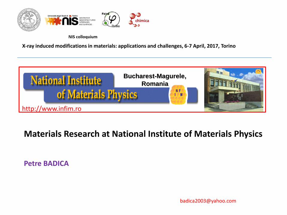
Romania: East of Europe, North of the Balkan Peninsula
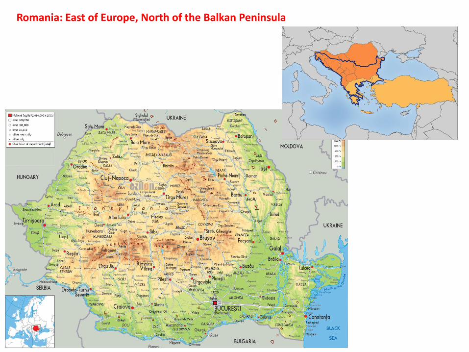
Located: 17 Km south from the Bucharest city center and 150 Km from Dracula Castle
DraculaCastle
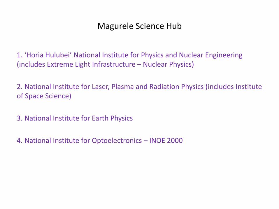
Magurele Science Hub
1. ‘Horia Hulubei’ National Institute for Physics and Nuclear Engineering (includes Extreme Light Infrastructure – Nuclear Physics)
2. National Institute for Laser, Plasma and Radiation Physics (includes Institute of Space Science)
3. National Institute for Earth Physics
4. National Institute for Optoelectronics – INOE 2000
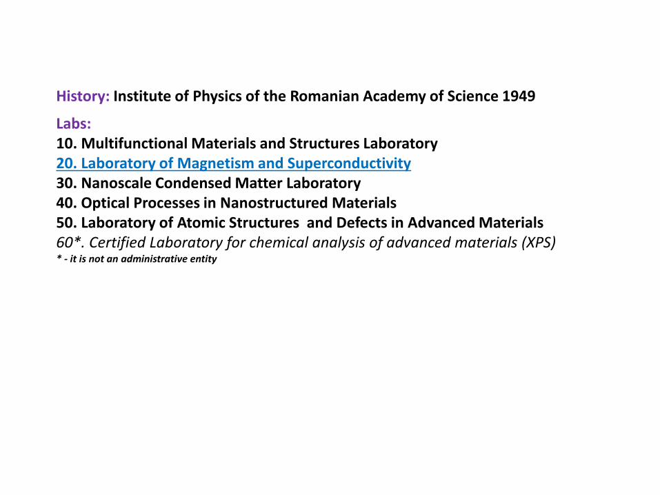
Labs:10. Multifunctional Materials and Structures Laboratory20. Laboratory of Magnetism and Superconductivity30. Nanoscale Condensed Matter Laboratory40. Optical Processes in Nanostructured Materials50. Laboratory of Atomic Structures and Defects in Advanced Materials60*. Certified Laboratory for chemical analysis of advanced materials (XPS)* - it is not an administrative entity
History: Institute of Physics of the Romanian Academy of Science 1949

Fields of interest:1. Cond matter – phenomena and processes in nano-dimensional, surface andinterface systems
2. Synthesis and characterization of nanomaterials and nanostructures3. Functional materials and structures with technological impact
A: Fundamental studies cond. matter1. Dimensional effects in nano-objects and cuantic layers2. Surfaces and interfaces in structured materials3. Electronic correlations and magnetic interactions4. Computational modeling and simulation of the dynamics microstructures5. Interaction between matter and radiation at micro and nano scales
B: Multifunctional nanostructures and materials1 – Materials for energy (generation, transport, conversion, storage)2 – Materials for applications from the high tech industry (materials for high frequency electronics MW, THz, materials for optoelectronics, transparentelectronics, materials for non-volatile memories, sensors for automatization andcontrol)3 – Materials for applications in biomedicine and environment protection (biocompatible and biofunctional materials, bio and chemical sensors and foto-catalysts)
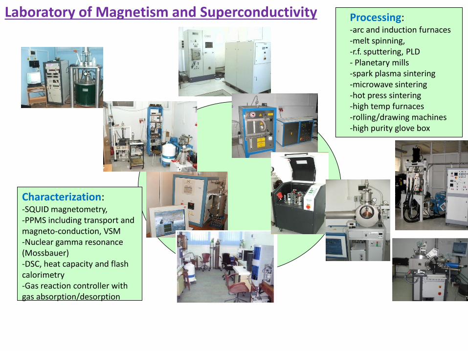
Laboratory of Magnetism and Superconductivity Processing:-arc and induction furnaces -melt spinning, -r.f. sputtering, PLD- Planetary mills-spark plasma sintering-microwave sintering-hot press sintering-high temp furnaces-rolling/drawing machines-high purity glove box
Characterization:-SQUID magnetometry, -PPMS including transport and magneto-conduction, VSM-Nuclear gamma resonance (Mossbauer)-DSC, heat capacity and flash calorimetry-Gas reaction controller with gas absorption/desorption
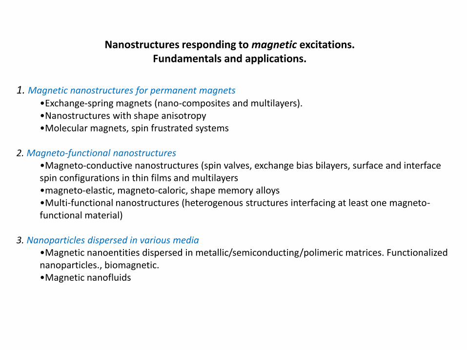
1. Magnetic nanostructures for permanent magnets•Exchange-spring magnets (nano-composites and multilayers). •Nanostructures with shape anisotropy•Molecular magnets, spin frustrated systems
2. Magneto-functional nanostructures•Magneto-conductive nanostructures (spin valves, exchange bias bilayers, surface and interface spin configurations in thin films and multilayers•magneto-elastic, magneto-caloric, shape memory alloys•Multi-functional nanostructures (heterogenous structures interfacing at least one magneto-functional material)
3. Nanoparticles dispersed in various media•Magnetic nanoentities dispersed in metallic/semiconducting/polimeric matrices. Functionalized nanoparticles., biomagnetic.•Magnetic nanofluids
Nanostructures responding to magnetic excitations. Fundamentals and applications.
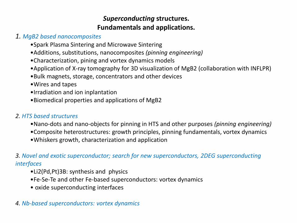
1. MgB2 based nanocomposites•Spark Plasma Sintering and Microwave Sintering •Additions, substitutions, nanocomposites (pinning engineering)•Characterization, pining and vortex dynamics models•Application of X-ray tomography for 3D visualization of MgB2 (collaboration with INFLPR)•Bulk magnets, storage, concentrators and other devices•Wires and tapes •Irradiation and ion inplantation•Biomedical properties and applications of MgB2
2. HTS based structures•Nano-dots and nano-objects for pinning in HTS and other purposes (pinning engineering)•Composite heterostructures: growth principles, pinning fundamentals, vortex dynamics•Whiskers growth, characterization and application
3. Novel and exotic superconductor; search for new superconductors, 2DEG superconducting interfaces
•Li2(Pd,Pt)3B: synthesis and physics•Fe-Se-Te and other Fe-based superconductors: vortex dynamics• oxide superconducting interfaces
4. Nb-based superconductors: vortex dynamics
Superconducting structures.Fundamentals and applications.
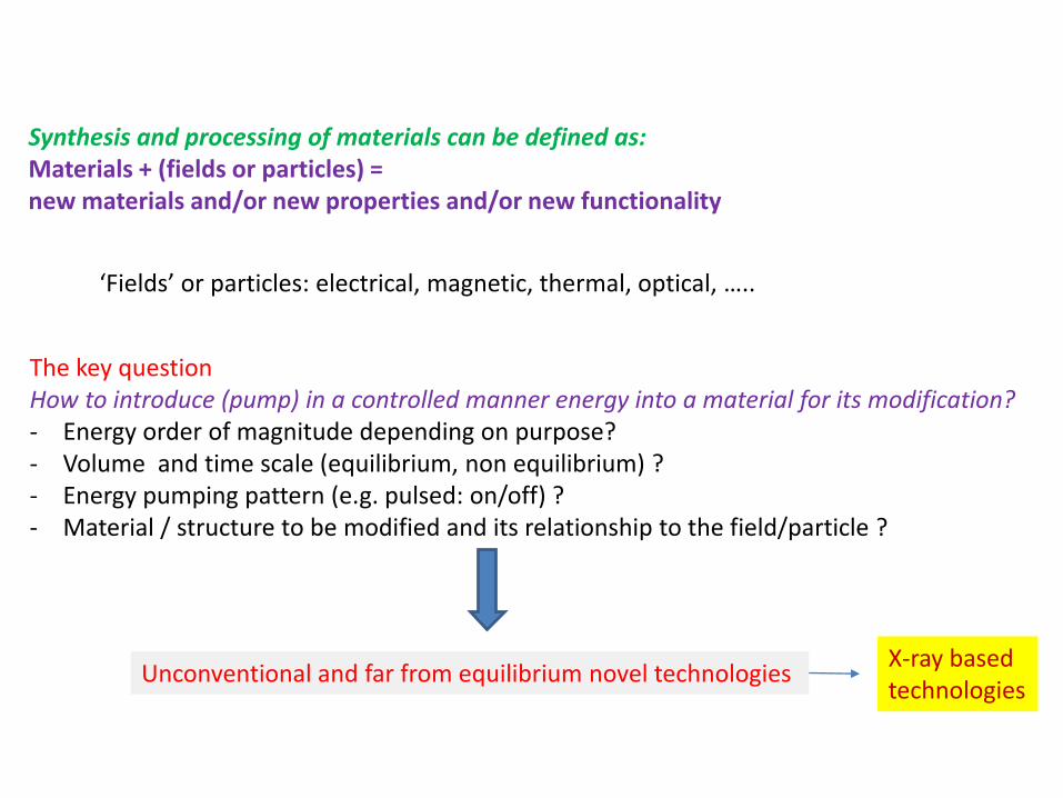
Synthesis and processing of materials can be defined as:Materials + (fields or particles) = new materials and/or new properties and/or new functionality
‘Fields’ or particles: electrical, magnetic, thermal, optical, …..
The key questionHow to introduce (pump) in a controlled manner energy into a material for its modification?- Energy order of magnitude depending on purpose?- Volume and time scale (equilibrium, non equilibrium) ?- Energy pumping pattern (e.g. pulsed: on/off) ?- Material / structure to be modified and its relationship to the field/particle ?
Unconventional and far from equilibrium novel technologiesX-ray basedtechnologies
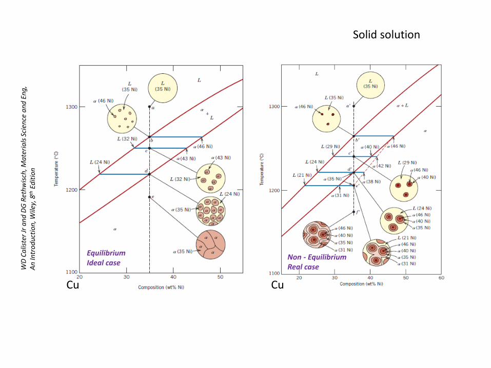
Cu Cu
EquilibriumIdeal case
Non - EquilibriumReal caseW
D C
alis
ter
Jra
nd
DG
Ret
hw
isch
, Ma
teri
als
Sci
ence
an
d E
ng
, A
n In
tro
du
ctio
n, W
iley,
8th
Edit
ion
Solid solution
WD Calister Jr and DG Rethwisch, Materials Science and Eng, An Introduction, Wiley, 8th Edition
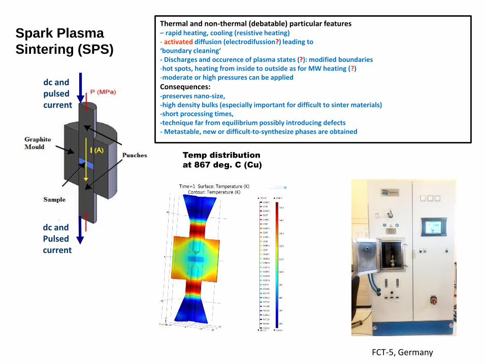
dc andPulsed current
dc andpulsed current
Spark Plasma
Sintering (SPS)
FCT-5, Germany
Temp distribution
at 867 deg. C (Cu)
Thermal and non-thermal (debatable) particular features – rapid heating, cooling (resistive heating)- activated diffusion (electrodifussion?) leading to ‘boundary cleaning‘- Discharges and occurence of plasma states (?): modified boundaries-hot spots, heating from inside to outside as for MW heating (?) -moderate or high pressures can be applied
Consequences:-preserves nano-size, -high density bulks (especially important for difficult to sinter materials)-short processing times, -technique far from equilibrium possibly introducing defects- Metastable, new or difficult-to-synthesize phases are obtained
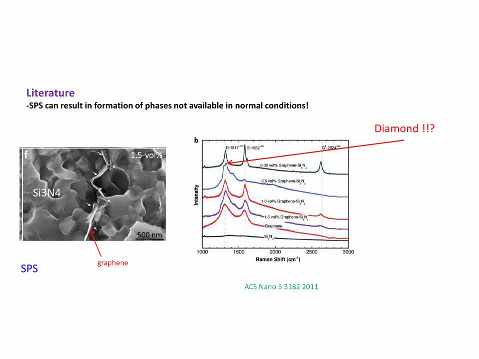
Literature-SPS can result in formation of phases not available in normal conditions!
SPSgraphene
Si3N4
Diamond !!?
ACS Nano 5 3182 2011
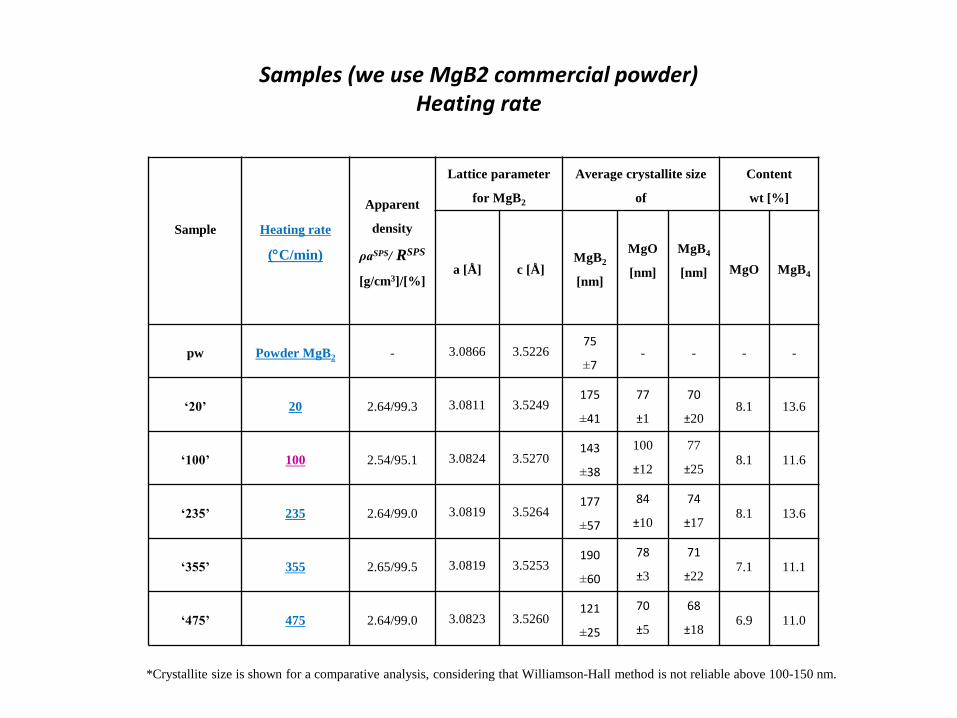
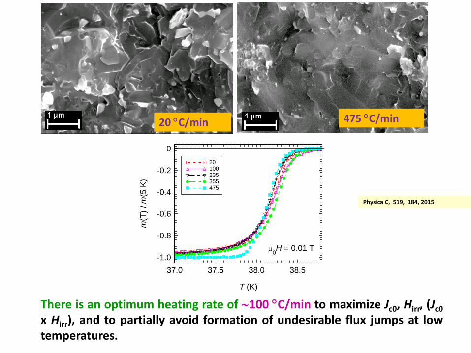
Samples (we use MgB2 commercial powder)Heating rate
Sample Heating rate
(C/min)
Apparent
density
ρaSPS/ RSPS
[g/cm3]/[%]
Lattice parameter
for MgB2
Average crystallite size
of
Content
wt [%]
a [Å] c [Å]MgB2
[nm]
MgO
[nm]
MgB4
[nm] MgO MgB4
pw Powder MgB2 - 3.0866 3.522675
±7- - - -
‘20’ 20 2.64/99.3 3.0811 3.5249175
±41
77
±1
70
±208.1 13.6
‘100’ 100 2.54/95.1 3.0824 3.5270143
±38
100
±12
77
±258.1 11.6
‘235’ 235 2.64/99.0 3.0819 3.5264177
±57
84
±10
74
±178.1 13.6
‘355’ 355 2.65/99.5 3.0819 3.5253190
±60
78
±3
71
±227.1 11.1
‘475’ 475 2.64/99.0 3.0823 3.5260121
±25
70
±5
68
±186.9 11.0
*Crystallite size is shown for a comparative analysis, considering that Williamson-Hall method is not reliable above 100-150 nm.
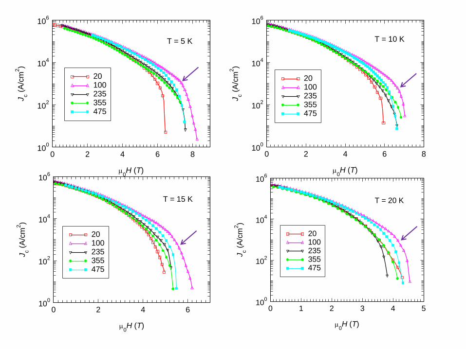
100
102
104
106
0 2 4 6 8
20100235355475
T = 5 K
0H (T)
Jc (
A/c
m2)
100
102
104
106
0 2 4 6 8
20100235355475
T = 10 K
0H (T)
Jc (
A/c
m2)
100
102
104
106
0 2 4 6
20100235355475
T = 15 K
0H (T)
Jc (
A/c
m2)
100
102
104
106
0 1 2 3 4 5
20100235355475
T = 20 K
0H (T)
Jc (
A/c
m2)
20 C/min 475 C/min
-1.0
-0.8
-0.6
-0.4
-0.2
0
37.0 37.5 38.0 38.5
20100235355475
0H = 0.01 T
T (K)
m(T
) / m
(5 K
)
There is an optimum heating rate of 100 C/min to maximize Jc0, Hirr, (Jc0
x Hirr), and to partially avoid formation of undesirable flux jumps at lowtemperatures.
Physica C, 519, 184, 2015
MgB2 by SPS for different on / offpulsed pattern of the current(work in progress)
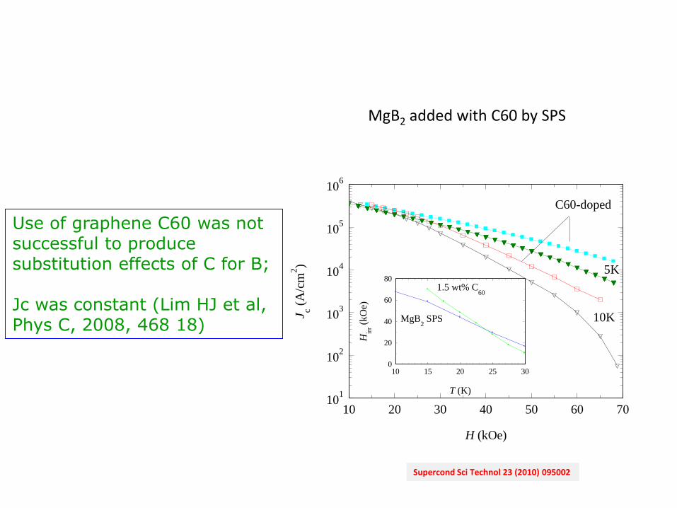
Use of graphene C60 was not successful to produce substitution effects of C for B;
Jc was constant (Lim HJ et al, Phys C, 2008, 468 18)
101
102
103
104
105
106
10 20 30 40 50 60 70
C60-doped
10K
5K
H (kOe)
J c (A
/cm
2)
0
20
40
60
80
10 15 20 25 30
1.5 wt% C60
MgB2 SPS
T (K)
Hir
r (k
Oe)
MgB2 added with C60 by SPS
Supercond Sci Technol 23 (2010) 095002
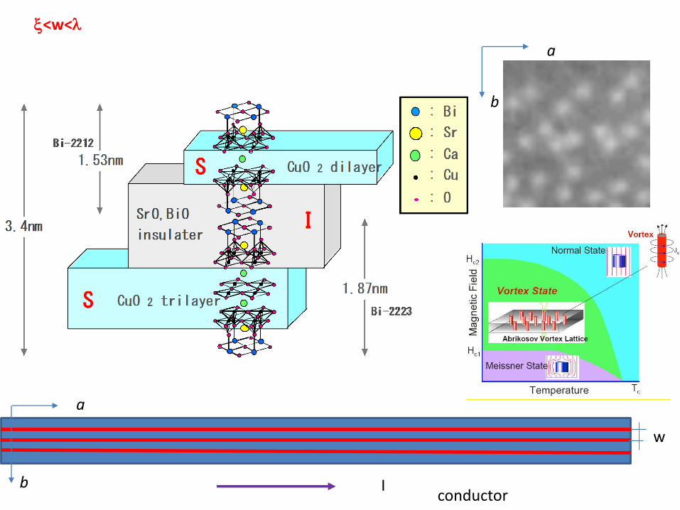
I
<w<
w
a
b
a
b
conductor
lateral
top
-0.75
-0.25
0 50 100 150
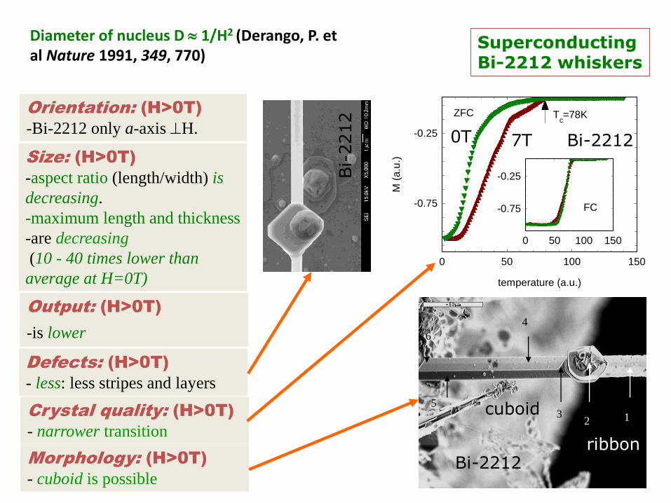
ZFC Tc=78K
temperature (a.u.)
M (
a.u
.)
-0.75
-0.25
0 50 100 150
FC
Size: (H>0T)
-aspect ratio (length/width) is
decreasing.
-maximum length and thickness
-are decreasing
(10 - 40 times lower than
average at H=0T)
Orientation: (H>0T)
-Bi-2212 only a-axis H.
Output: (H>0T)
-is lower
Defects: (H>0T)
- less: less stripes and layers
Crystal quality: (H>0T)
- narrower transition
Morphology: (H>0T)
- cuboid is possible
123
4
5
6
0T 7T
ribbon
cuboid
Bi-
2212
Bi-2212
Bi-2212
SuperconductingBi-2212 whiskers
Diameter of nucleus D 1/H2 (Derango, P. et al Nature 1991, 349, 770)
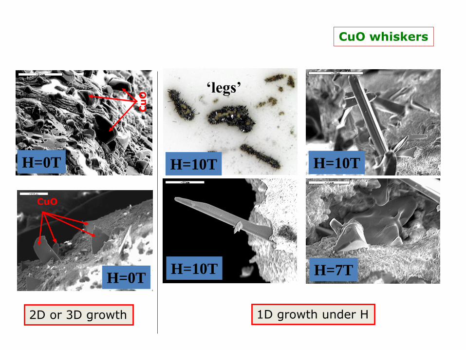
CuO whiskers
H=0T
H=0T
2D or 3D growth
CuO
Cu
O
‘legs’
H=10T H=10T
H=10T H=7T
1D growth under H
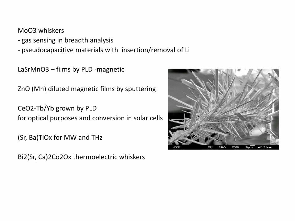
MoO3 whiskers
- gas sensing in breadth analysis
- pseudocapacitive materials with insertion/removal of Li
LaSrMnO3 – films by PLD -magnetic
ZnO (Mn) diluted magnetic films by sputtering
CeO2-Tb/Yb grown by PLD
for optical purposes and conversion in solar cells
(Sr, Ba)TiOx for MW and THz
Bi2(Sr, Ca)2Co2Ox thermoelectric whiskers

Thank you for your attention !!!!