Embed Size (px)
Citation preview

Application Note 1 Rev. 0.5www.infineon.com 2016-12-22
BTN8960 /62 /80 /82High Current PN Half Bridge
About this document
Scope and purposeThis Application Note is intended to provide information and hints for a high current design, using PWMcontrol with the NovalithIC™ half-bridge family BTN89xy for the automotive environment.
Note: The following information is only given to help with the implementation of the device and shall not be regarded as a description or warranty of a certain functionality, condition or quality of the device.
1 AbstractThis family contains one P-channel high-side MOSFET and one N-channel low-side MOSFETwith an integrateddriver IC in one package. The NovalithIC™ is the interface between the microcontroller and the motor,equipped with diagnostic and protection functions.
Figure 1 Block Diagram BTN89xy
As both the high-side and low side switch are placed on one single leadframe this results in many systembenefits: Resulting from the low distance between the high-side MOSFET and the low-side MOSFETthe strayinductances between them is minimal thus minimizing negative voltage spikes at OUT during switching andimproving EMC. As the voltage level of the leadframe is on the output of the half-bridge, only one single cooling
IS
SR
INH
IN
GND
OUT
VS
Gate DriverHS
SlewrateAdjustment
Digital Logic
Undervolt.detection
Overtemp.detection
Overcurr.Detection
LS
Overcurr.Detection
HS
CurrentSense
Gate DriverLS
LS off HS off
High Current PN Half Bridge

Application Note 2 Rev. 0.5 2016-12-22
BTN8960 /62 /80 /82High Current PN Half Bridge
Abstract
area is required (on OUT potential) for the device, thus being used for both a high-side or low-side currentswitching. For a state of the art N-channel solution, usually two cooling areas are required, each for the high-side and low-side MOSFET.Due to the p-channel highside switch the need for a charge pump is eliminated thus minimizing EMI.Interfacing to a microcontroller is made easy by the integrated driver IC which features logic level inputs,diagnosis with current sense, slew rate adjustment, dead time generation and protection againstovertemperature, undervoltage, overcurrent and short circuit.

Application Note 3 Rev. 0.5 2016-12-22
BTN8960 /62 /80 /82High Current PN Half Bridge
About this document . . . . . . . . . . . . . . . . . . . . . . . . . . . . . . . . . . . . . . . . . . . . . . . . . . . . . . . . . . . . 1
1 Abstract . . . . . . . . . . . . . . . . . . . . . . . . . . . . . . . . . . . . . . . . . . . . . . . . . . . . . . . . . . . . . . . . . . . . . . . 1
Table of Contents . . . . . . . . . . . . . . . . . . . . . . . . . . . . . . . . . . . . . . . . . . . . . . . . . . . . . . . . . . . . . . . 3
2 Motor Configurations . . . . . . . . . . . . . . . . . . . . . . . . . . . . . . . . . . . . . . . . . . . . . . . . . . . . . . . . . . . . 52.1 Half-bridge configuration for mono-directional motor control . . . . . . . . . . . . . . . . . . . . . . . . . . . . . . . . 52.2 H-Bridge configuration for bidirectional motor control . . . . . . . . . . . . . . . . . . . . . . . . . . . . . . . . . . . . . . . 6
3 Parasitic Inductance . . . . . . . . . . . . . . . . . . . . . . . . . . . . . . . . . . . . . . . . . . . . . . . . . . . . . . . . . . . . 73.1 Measuring signals at NovalithICTM . . . . . . . . . . . . . . . . . . . . . . . . . . . . . . . . . . . . . . . . . . . . . . . . . . . . . . . . . . 7
4 Design Guideline . . . . . . . . . . . . . . . . . . . . . . . . . . . . . . . . . . . . . . . . . . . . . . . . . . . . . . . . . . . . . . . . 94.1 Schematic and layout design rules . . . . . . . . . . . . . . . . . . . . . . . . . . . . . . . . . . . . . . . . . . . . . . . . . . . . . . . . . 94.2 DC-link capacitor . . . . . . . . . . . . . . . . . . . . . . . . . . . . . . . . . . . . . . . . . . . . . . . . . . . . . . . . . . . . . . . . . . . . . . . . 114.2.1 Calculation of the DC-link capacitor and Pi-filter . . . . . . . . . . . . . . . . . . . . . . . . . . . . . . . . . . . . . . . . . . 114.2.2 Undervoltage toggling . . . . . . . . . . . . . . . . . . . . . . . . . . . . . . . . . . . . . . . . . . . . . . . . . . . . . . . . . . . . . . . . . . 144.3 Ground references . . . . . . . . . . . . . . . . . . . . . . . . . . . . . . . . . . . . . . . . . . . . . . . . . . . . . . . . . . . . . . . . . . . . . . . 164.4 Driving inductive loads over long wires . . . . . . . . . . . . . . . . . . . . . . . . . . . . . . . . . . . . . . . . . . . . . . . . . . . . 174.4.1 PWM operation . . . . . . . . . . . . . . . . . . . . . . . . . . . . . . . . . . . . . . . . . . . . . . . . . . . . . . . . . . . . . . . . . . . . . . . . 174.4.2 Current sense . . . . . . . . . . . . . . . . . . . . . . . . . . . . . . . . . . . . . . . . . . . . . . . . . . . . . . . . . . . . . . . . . . . . . . . . . . 184.5 Reverse polarity protection . . . . . . . . . . . . . . . . . . . . . . . . . . . . . . . . . . . . . . . . . . . . . . . . . . . . . . . . . . . . . . . 184.6 Cooling . . . . . . . . . . . . . . . . . . . . . . . . . . . . . . . . . . . . . . . . . . . . . . . . . . . . . . . . . . . . . . . . . . . . . . . . . . . . . . . . . 18
5 Current Sense Improvement . . . . . . . . . . . . . . . . . . . . . . . . . . . . . . . . . . . . . . . . . . . . . . . . . . . . . 205.1 Characteristic of the dkILIS . . . . . . . . . . . . . . . . . . . . . . . . . . . . . . . . . . . . . . . . . . . . . . . . . . . . . . . . . . . . . . . . 205.1.1 Supply voltage dependency of dkILIS . . . . . . . . . . . . . . . . . . . . . . . . . . . . . . . . . . . . . . . . . . . . . . . . . . . . . 205.1.2 TC 1000 life time tests . . . . . . . . . . . . . . . . . . . . . . . . . . . . . . . . . . . . . . . . . . . . . . . . . . . . . . . . . . . . . . . . . . 215.1.3 Temperature drift of the dkILIS . . . . . . . . . . . . . . . . . . . . . . . . . . . . . . . . . . . . . . . . . . . . . . . . . . . . . . . . . . . 215.2 Offset compensation . . . . . . . . . . . . . . . . . . . . . . . . . . . . . . . . . . . . . . . . . . . . . . . . . . . . . . . . . . . . . . . . . . . . . 235.3 Device specific dkILIS . . . . . . . . . . . . . . . . . . . . . . . . . . . . . . . . . . . . . . . . . . . . . . . . . . . . . . . . . . . . . . . . . . . . . 245.4 Device fine dkILIS and temperature compensation . . . . . . . . . . . . . . . . . . . . . . . . . . . . . . . . . . . . . . . . . . . 255.4.1 An example of the IIS failure with a rough temperature estimation . . . . . . . . . . . . . . . . . . . . . . . . . . 275.5 IS-pin current sensing and fault detection . . . . . . . . . . . . . . . . . . . . . . . . . . . . . . . . . . . . . . . . . . . . . . . . . . 275.5.1 Current sensing concepts in applications . . . . . . . . . . . . . . . . . . . . . . . . . . . . . . . . . . . . . . . . . . . . . . . . . 275.5.1.1 BTN89xy - advanced current sense and fault diagnosis . . . . . . . . . . . . . . . . . . . . . . . . . . . . . . . . . . 285.5.1.2 BTN79xy current sense limitations . . . . . . . . . . . . . . . . . . . . . . . . . . . . . . . . . . . . . . . . . . . . . . . . . . . . 295.5.2 Fault detection . . . . . . . . . . . . . . . . . . . . . . . . . . . . . . . . . . . . . . . . . . . . . . . . . . . . . . . . . . . . . . . . . . . . . . . . 305.5.2.1 Temperature drift of the IS-pin’s current in fault condition IIS(lim) . . . . . . . . . . . . . . . . . . . . . . . . . 355.5.2.2 Failure detection flow chart . . . . . . . . . . . . . . . . . . . . . . . . . . . . . . . . . . . . . . . . . . . . . . . . . . . . . . . . . . 375.5.2.3 Lowpass filtered current sense signal . . . . . . . . . . . . . . . . . . . . . . . . . . . . . . . . . . . . . . . . . . . . . . . . . . 38
6 Switching Timing . . . . . . . . . . . . . . . . . . . . . . . . . . . . . . . . . . . . . . . . . . . . . . . . . . . . . . . . . . . . . . 416.1 BTN8982TA . . . . . . . . . . . . . . . . . . . . . . . . . . . . . . . . . . . . . . . . . . . . . . . . . . . . . . . . . . . . . . . . . . . . . . . . . . . . . 436.1.1 Timing behavior for rising edge on high-side switch . . . . . . . . . . . . . . . . . . . . . . . . . . . . . . . . . . . . . . . 436.1.2 Timing behavior for falling edge on high-side switch . . . . . . . . . . . . . . . . . . . . . . . . . . . . . . . . . . . . . . 446.1.3 Timing behavior for rising edge on low-side switch . . . . . . . . . . . . . . . . . . . . . . . . . . . . . . . . . . . . . . . . 466.1.4 Timing behavior for falling edge on low-side switch . . . . . . . . . . . . . . . . . . . . . . . . . . . . . . . . . . . . . . . 476.2 BTN8962TA . . . . . . . . . . . . . . . . . . . . . . . . . . . . . . . . . . . . . . . . . . . . . . . . . . . . . . . . . . . . . . . . . . . . . . . . . . . . . 486.2.1 Timing behavior for rising edge on high-side switch . . . . . . . . . . . . . . . . . . . . . . . . . . . . . . . . . . . . . . . 48
Table of Contents

Application Note 4 Rev. 0.5 2016-12-22
BTN8960 /62 /80 /82High Current PN Half Bridge
6.2.2 Timing behavior for falling edge on high-side switch . . . . . . . . . . . . . . . . . . . . . . . . . . . . . . . . . . . . . . 496.2.3 Timing behavior for rising edge on low-side switch . . . . . . . . . . . . . . . . . . . . . . . . . . . . . . . . . . . . . . . . 516.2.4 Timing behavior for falling edge on low-side switch . . . . . . . . . . . . . . . . . . . . . . . . . . . . . . . . . . . . . . . 526.3 Error of total delay time . . . . . . . . . . . . . . . . . . . . . . . . . . . . . . . . . . . . . . . . . . . . . . . . . . . . . . . . . . . . . . . . . . 526.4 Delay time calibration . . . . . . . . . . . . . . . . . . . . . . . . . . . . . . . . . . . . . . . . . . . . . . . . . . . . . . . . . . . . . . . . . . . . 546.4.1 Output voltage based calibration . . . . . . . . . . . . . . . . . . . . . . . . . . . . . . . . . . . . . . . . . . . . . . . . . . . . . . . . 546.4.2 Current sense based calibration . . . . . . . . . . . . . . . . . . . . . . . . . . . . . . . . . . . . . . . . . . . . . . . . . . . . . . . . . 556.5 ADC Timing for current measurement . . . . . . . . . . . . . . . . . . . . . . . . . . . . . . . . . . . . . . . . . . . . . . . . . . . . . 566.5.1 Current sense ADC timing . . . . . . . . . . . . . . . . . . . . . . . . . . . . . . . . . . . . . . . . . . . . . . . . . . . . . . . . . . . . . . . 566.5.2 Offset current calibration ADC timing . . . . . . . . . . . . . . . . . . . . . . . . . . . . . . . . . . . . . . . . . . . . . . . . . . . . 586.6 Allowed PWM setup for current sense ADC measurements . . . . . . . . . . . . . . . . . . . . . . . . . . . . . . . . . . . 596.6.1 BTN8962TA . . . . . . . . . . . . . . . . . . . . . . . . . . . . . . . . . . . . . . . . . . . . . . . . . . . . . . . . . . . . . . . . . . . . . . . . . . . . 606.6.2 BTN8982TA . . . . . . . . . . . . . . . . . . . . . . . . . . . . . . . . . . . . . . . . . . . . . . . . . . . . . . . . . . . . . . . . . . . . . . . . . . . . 616.6.3 Example calculation . . . . . . . . . . . . . . . . . . . . . . . . . . . . . . . . . . . . . . . . . . . . . . . . . . . . . . . . . . . . . . . . . . . . 62
7 Power Dissipation . . . . . . . . . . . . . . . . . . . . . . . . . . . . . . . . . . . . . . . . . . . . . . . . . . . . . . . . . . . . . . 647.1 Power dissipation of the control chip (top chip) . . . . . . . . . . . . . . . . . . . . . . . . . . . . . . . . . . . . . . . . . . . . . 647.2 Conduction power dissipation . . . . . . . . . . . . . . . . . . . . . . . . . . . . . . . . . . . . . . . . . . . . . . . . . . . . . . . . . . . . 647.3 Power dissipation due to switching . . . . . . . . . . . . . . . . . . . . . . . . . . . . . . . . . . . . . . . . . . . . . . . . . . . . . . . . 657.4 Entire power dissipation of the MOSFETs . . . . . . . . . . . . . . . . . . . . . . . . . . . . . . . . . . . . . . . . . . . . . . . . . . 667.4.1 PWM control and the duty cycle constraints . . . . . . . . . . . . . . . . . . . . . . . . . . . . . . . . . . . . . . . . . . . . . . 677.4.2 Entire power dissipation in the actuator MOSFET . . . . . . . . . . . . . . . . . . . . . . . . . . . . . . . . . . . . . . . . . 677.4.3 Entire power dissipation in the freewheeling MOSFET . . . . . . . . . . . . . . . . . . . . . . . . . . . . . . . . . . . . . 687.5 Entire power dissipation in the NovalithICTM . . . . . . . . . . . . . . . . . . . . . . . . . . . . . . . . . . . . . . . . . . . . . . . . 687.6 Simplifications . . . . . . . . . . . . . . . . . . . . . . . . . . . . . . . . . . . . . . . . . . . . . . . . . . . . . . . . . . . . . . . . . . . . . . . . . . 68
8 Thermal Performance . . . . . . . . . . . . . . . . . . . . . . . . . . . . . . . . . . . . . . . . . . . . . . . . . . . . . . . . . . 708.1 Zth simulation results . . . . . . . . . . . . . . . . . . . . . . . . . . . . . . . . . . . . . . . . . . . . . . . . . . . . . . . . . . . . . . . . . . . . 718.2 Thermal RC-network . . . . . . . . . . . . . . . . . . . . . . . . . . . . . . . . . . . . . . . . . . . . . . . . . . . . . . . . . . . . . . . . . . . . . 728.2.1 Parameters for BTN8960/62 . . . . . . . . . . . . . . . . . . . . . . . . . . . . . . . . . . . . . . . . . . . . . . . . . . . . . . . . . . . . . 748.2.2 Parameters for BTN8980/82 . . . . . . . . . . . . . . . . . . . . . . . . . . . . . . . . . . . . . . . . . . . . . . . . . . . . . . . . . . . . . 75
9 Revision History . . . . . . . . . . . . . . . . . . . . . . . . . . . . . . . . . . . . . . . . . . . . . . . . . . . . . . . . . . . . . . . 78

Application Note 5 Rev. 0.5 2016-12-22
BTN8960 /62 /80 /82High Current PN Half Bridge
Motor Configurations
2 Motor ConfigurationsElectrical motors are built with various architectures. Mechanically commutated motors with brushes, socalled DC motors or electrically commutated motors, so called BLDC motors (BrushLess DC motors). TheNovalithIC™ family can support all of them due to, the flexibility of the half-bridge concept. Using NovalithIC™ controlling a DC-motor has the following advantages: • Extremely low parasitic inductances between high-side and low-side MOSFET.• Optimized switching performance of the MOSFET’s to reduce power losses and EMC emission.• Driving the motor with PWM for torque and speed control.• Integrated freewheeling transistor.• Integrated current measurement.• Integrated diagnosis and protection.• Microcontroller -compatible input pins.• Small and PCB-area saving package.
2.1 Half-bridge configuration for mono-directional motor controlFigure 2 shows the design of a mono-directional motor control with NovalithIC™. In most cases, the motor isconnected between “OUT” and “GND”. This is because the chassis of a car is “GND”, and therefore a short to“GND” is much more probable than a short to “Vs”. For this reason it is statistically safer with a motorconnected to “GND”, because if a short occurs in this case, the motor is not running. Generally, it is also possible to use the NovalithIC™ to drive the motor between “OUT” and “Vs”. The inverted“IN” signal must be respected.
Figure 2 Application circuit for a monodirectional motor with BTN89xy
M
XC866
TLE 4278G
VS
I/O
Reset
Vdd
Vss
WO
RO
Q
D GND
I
Microcontroller Reverse Polarity Protection
(IPD90P03P4L-04)
Voltage Regulator
C9
100nF
CD
47nF
CQ
22µF
C10
470µF/
R3
10kΩ
DZ 1
10V
R1
10kΩ
R2
10kΩ
R11
0..51kΩ
R12
1kΩ
I/OI/OI/O
CI
470nF
CIS
1nF
CO 2V
220nF
C1
47µF/100µF
L1
INH
IN
IS
SR
BTN89xxVS
OUT
GND
COUT
220nF
C2
100nF
1000µF

Application Note 6 Rev. 0.5 2016-12-22
BTN8960 /62 /80 /82High Current PN Half Bridge
Motor Configurations
2.2 H-Bridge configuration for bidirectional motor controlWith the NovalithIC™ family it is easy to build an H-bridge for bidirectional DC motor control by simplycombining two devices in H-bridge configuration, as it is shown in Figure 3.
Figure 3 Application circuit for a bidirectional motor with BTN89xy H-bridge
optional
M
XC866 TLE 4278G
I/O
Reset
Vdd
Vss
WO
RO
Q
D GND
I
Microcontroller Voltage Regulator
C19
100nF
CD
47nF
CQ
22µF
C10
470µF/R11
10kΩ
R12
10kΩ
R111
0..51kΩ
R112
1kΩ
I /OI/O
CI
470nF
C1O 2V
220nF
C1OUT
220nF
C2 O2V
220nF
C2OUT
220nFC29
100nF
R211
0..51kΩ
I /OA/D
R22
10kΩ
R21
10kΩ
R212
1kΩ
A/D
INH
IN
IS
SR
BTN89xyVS
OUT
GND
INH
IN
IS
SR
BTN89xyVS
OUT
GND
VS
Reverse Polarity Protection
(IPD90P03P4L-04)
R3
10kΩ
DZ1
10V
C1
47µF/100µF
L1
C22
100nF
C2IS
1nFC1IS
1nFC12
100nF
1000µF

Application Note 7 Rev. 0.5 2016-12-22
BTN8960 /62 /80 /82High Current PN Half Bridge
Parasitic Inductance
3 Parasitic InductanceIn high-current applications, which the NovalithIC™ family is designed for, special care must be taken forparasitic inductors. The same is valid in case of very high frequencies, which are interesting with regard to EMCconsiderations.Each kind of wire in the application is an inductor, e.g. PCB wires, bond wires, etc. The wire inductance can beestimated with • 1mm PCB wire length approximately 1.2 nH• 1 PCB via approximately 1 nHThe voltage drop of a wire can be calculated in the following way:
(3.1)
As can be seen from this equation, care must be taken with the parasitic wire inductors with increasing currentand decreasing switching time. The NovalithIC™ is designed to switch high currents very quickly. This meansin applications with NovalithIC™, the parasitic inductors are relevant and special care must be taken.
3.1 Measuring signals at NovalithICTM
The parasitic inductance also has an influence on the measurement results. To measure the true signals at theNovalithIC™ it is mandatory to position the measurement probes directly at the device, as it is shown inFigure 4. The probe is connected directly to the Vs-pin of the NovalithIC™ and the reference signal directly tothe GND-pin of the device.
Figure 4 Measuring Vs with Probe and Reference Directly Connected to NovalithICTM
dtdILU L ⋅=

Application Note 8 Rev. 0.5 2016-12-22
BTN8960 /62 /80 /82High Current PN Half Bridge
Parasitic Inductance
Doing so enables to monitoring of the NovalithIC™ supply voltage when high currents are switched. Forexample when a short-circuit current is switched, this is the only possibility for measurement if the DC-linkcapacitor is sufficient to keep the supply voltage above the undervoltage detection threshold (also seeChapter 4.2).

Application Note 9 Rev. 0.5 2016-12-22
BTN8960 /62 /80 /82High Current PN Half Bridge
Design Guideline
4 Design GuidelineFor a safe and sufficient motor control design, discrete components are needed. Some of them must bededicated to the motor application and some to the NovalithIC™.
4.1 Schematic and layout design rulesFigure 5 and Figure 6 show an example of a schematic plus a corresponding layout for a half-bridge motorcontrol with NovalithIC™.The best performance in terms of parasitic inductance and EMC can be reached with a GND plane, which westrongly recommend be used.
Figure 5 Example of a half-bridge schematic with NovalithICTM
Important design and layout rules:The basis for the following items is the parasitic inductance of electrical wires, as described in Chapter 3.• C10, so called DC-link capacitor: This electrolytic capacitor is required to keep the voltage ripple at the VS-
pin of the NovalithIC™ low during switching operation (the measurement procedure for the supply voltage is described in Chapter 3.1). It is strongly recommended that the voltage ripple at the NovalithIC™ Vs-pin to GND-pin be kept below 1 V peak-to-peak. The value of C10 must be aligned accordingly. See Equation (4.9).Most electrolytic capacitors are less effective at cold temperatures. It must be assured that C10 is also effective under the worst case conditions of the application. The layout is very important. As shown in Figure 6, the capacitor C10 must be positioned with very short wiring at the NovalithIC™. This must be done to keep the parasitic inductors of the PCB-wires as small as possible.
• C9: This ceramic capacitor supports C10 to keep the supply voltage ripple low and covers the fast transients between the Vs-pin and the GND-pin. The value of this ceramic capacitor must be chosen so that fast Vs-ripple at the NovalithIC™ does not exceed 1 V peak-to-peak.The layout wiring for C9 must be shorter than for C10 to the NovalithIC™ to keep the parasitic PCB-wire inductance as small as possible. In addition the parasitic inductance could be kept low by placing at least two vias for the connection to the GND-layer.
• C_O2V: This ceramic capacitor is important for EMI in order to avoid entering electromagnetic disturbances into the NovalithIC™ as much as possible. Good results have been achieved with a value of 220 nF.In terms of layout, it is important to place this capacitor between “OUT” and “Vs” without significant additional wiring from C_O2V to the Vs- and OUT-line.
• C_OUT: This ceramic capacitor helps improve the EMI and the ESD performance of the application. Good results have been achieved with a value of 220 nF.
47μF

Application Note 10 Rev. 0.5 2016-12-22
BTN8960 /62 /80 /82High Current PN Half Bridge
Design Guideline
To keep the RF and ESD out of the board, the capacitor is most effective when positioned directly on the board connector. In addition, the parasitic inductance could be kept low by placing at least two vias for the connection to the GND-layer.
• C1: This ceramic capacitor helps to improve the EMI and the ESD performance. In combination with L1 and C10 plus C9 a Pi-filter improves the electromagnetic emission on the Vs-line.Layout rules are the same as for C_OUT.
Figure 6 Example of an half-bridge layout with NovalithICTM (not true to scale)

Application Note 11 Rev. 0.5 2016-12-22
BTN8960 /62 /80 /82High Current PN Half Bridge
Design Guideline
Other components:• T1, D1 and R3: Reverse polarity protection. See Chapter 4.5.• R11: Slew rate resistor according to data sheet.• C2: Stabilization for slew rate resistor (R11). • R12: Resistor to generate a current sensing voltage from the IS current. • C_IS: Ceramic capacitor for EMI improvement. GND connection with at least two GND-vias. A good value is
1 nF.In case the current should be measured during the PWM-phase, this capacitor must be adapted to the ON-time inside the PWM-phase.
• R1 and R2: Device protection in case of µC pins shorted to Vs.
4.2 DC-link capacitorFor the stability of the DC-link voltage a sufficient capacitor is mandatory (in Figure 2, Figure 3 and Figure 5it is C10). This is one of the most important component in a motor design with semiconductor switches. The DC-link capacitor could be insufficient, because:• The capacitor value is too small.• The ESR of the capacitor is too high.• When cold the capacitor value is too small.• The distance between the DC-link capacitor and the NovalithIC™ is too large.• The wiring between the DC-link capacitor and the NovalithIC™ is too long (see Chapter 3).The value must be chosen carefully, taking the undervoltage toggling into account, which is described inChapter 4.2.2.
4.2.1 Calculation of the DC-link capacitor and Pi-filterAs already mentioned in the design- and layout-rules of Figure 5 the voltage ripple at the NovalithIC™ Vs-pinmust not exceed 1 V peak-to-peak. The necessary DC-link capacitor can be estimated in the following way:Motor control with PWM means for the DC-link voltage to provide energy pulses during the “ON-phase” of thePWM cycle. The DC-link pulses are shown in Figure 7. This energy must be provided by the DC-link capacitor. This can generally be described with
(4.1)
(4.2)
The voltage at the DC-link capacitor consists of the DC-part and the delta voltage from the supply ripple:
(4.3)
TPVCE ⋅=⋅⋅= 2
21
linkDCCC −=
SDCS VVV Δ+= ,

Application Note 12 Rev. 0.5 2016-12-22
BTN8960 /62 /80 /82High Current PN Half Bridge
Design Guideline
The total power in this system consists of the DC-power plus the power of the energy pulse (Epulse), whichprovides the energy to the motor during the ON-phase of the half bridge.
(4.4)
The maximum pulse length is determined by the PWM frequency, theoretically at a duty cycle of 100%:
(4.5)
Figure 7 PWM control (PWM = IN-pin-signal, IM = motor current and VS = VS-pin-voltage @ NovalithIC)
PPP DC Δ+=
PWMPWMpulse f
TTT 1===
∆IOUT
Epulse
tPWM
IM
t
IOUT,min
TPWM
Vs
t
∆VS
VS,DC
ON

Application Note 13 Rev. 0.5 2016-12-22
BTN8960 /62 /80 /82High Current PN Half Bridge
Design Guideline
Insertion of Equation (4.2) to Equation (4.5) into Equation (4.1)
(4.6)
(4.7)
(4.8)
Finally the equation to calculate the DC-link capacitor is:
(4.9)
Based on Equation (4.1) and referring to the energy of on single pulse, as marked with Epulse (≈ ΔP • TPWM) inFigure 7:
(4.10)
The DC-link capacitor is primarily the energy buffer for the switching process of the PWM motor control.Secondly it is part of the Pi-filter. This means first the DC-link capacitor must be calculated according toEquation (4.9). Based on this, it is recommended that the second capacitor of the Pi-filter C1 be estimatedwith:
(4.11)
Generally the border frequency of the L1-C1-filter is determined with
(4.12)
PWMDCSDCSlinkDC TPPVVCE ⋅Δ+=Δ+⋅⋅= − )()(21 2
,
PWMPWMDCSSDCSDCSlinkDC TPTPVVVVC ⋅Δ+⋅=Δ+Δ⋅⋅+⋅⋅ − )2(21 2
,2,
PW MPW MDCSlinkDCSDCSlinkDCDCSlinkDC TPTPVCVVCVC ⋅Δ+⋅=Δ⋅⋅+Δ⋅⋅+⋅⋅ −−−2
,2, 2
121
negligible
SDCS
PWMlinkDC VV
TPC
Δ⋅⋅Δ
≥−,
)21( min, OUTOUTSnomS IIVIVP ΔΔ +⋅≈⋅=
101 101
101 CCC linkDC ⋅=⋅= −
1121
CLf g
⋅⋅⋅=
Π

Application Note 14 Rev. 0.5 2016-12-22
BTN8960 /62 /80 /82High Current PN Half Bridge
Design Guideline
We recommend setting the border frequency fg to half the value of the PWM -frequency fPWM.
(4.13)
(4.14)
Summary:First calculate the DC-link capacitor with Equation (4.9).Second calculate the other capacitor of the Pi-filter with Equation (4.11).Then calculate the inductor of the Pi-filter with Equation (4.14).And last but not least, do not forget the important layout rules and how to measure the supply voltagecorrectly.
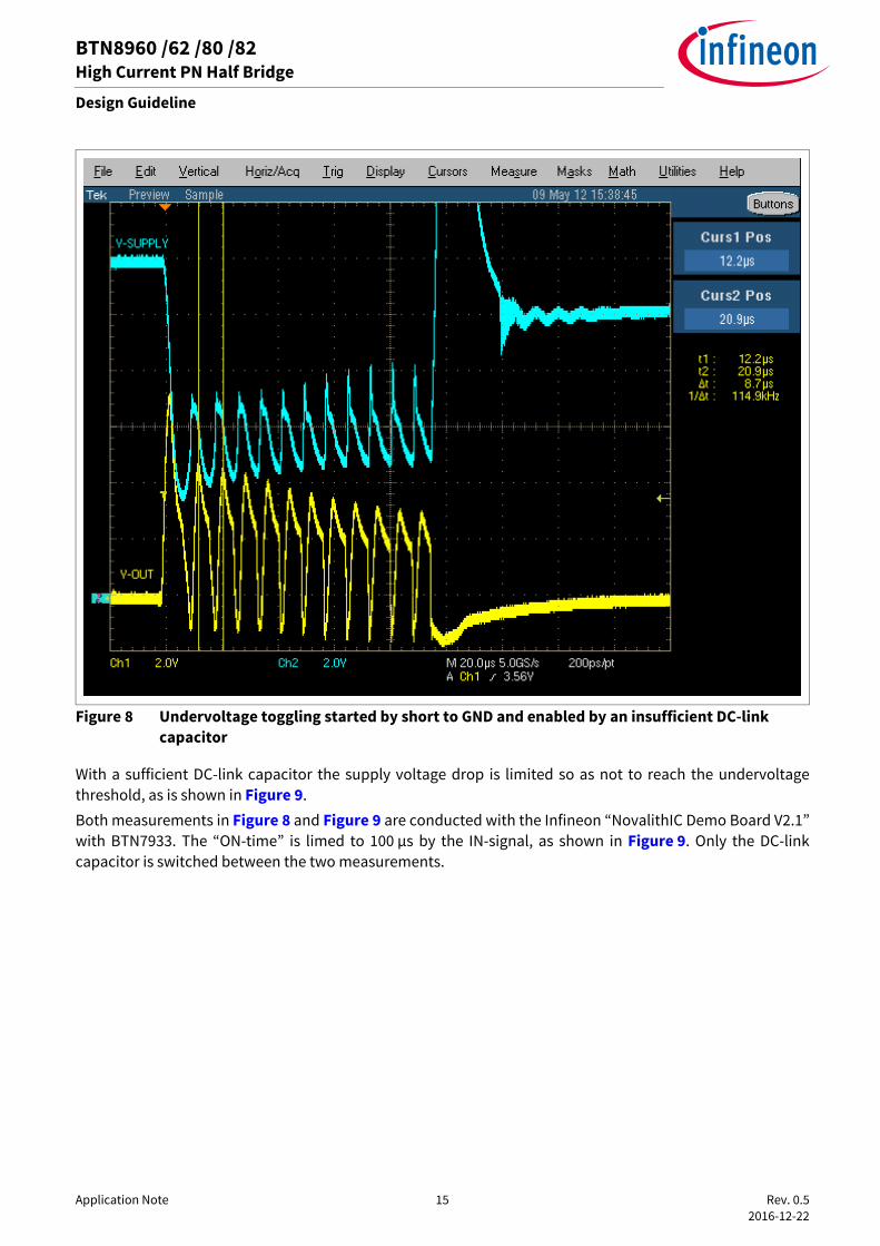
4.2.2 Undervoltage togglingThe power supply cable of most modules in a car are several meters long. The longer the supply cable is, thehigher its parasitic inductance. In addition, most modules have a Pi-filter at the supply line with a inductor forEMC reasons. The sum of the supply line inductances have a significant influence on the Vs-voltage. Whenswitching the motor ON during a normal motor start or PWM control, with a insufficient DC-link capacitor thesupply voltage drops below the undervoltage threshold and the NovalithIC™ is switched to tristate. The supplyvoltage recovers above the undervoltage threshold and the NovalithIC™ switches on again, again droppingbelow the undervoltage threshold ... This effect can result in frequencies higher than 100 kHz, as is shown in Figure 8. The device will be damagedby the power dissipation of the switching losses, which is faster than the reaction time of the over temperatureshut down, because of the high switching frequency. The undervoltage toggling will be worse if the OUT is shorted to GND.
1121
21
CLff PWMg
⋅⋅⋅=⋅=
Π
12211
CfL
PWM ⋅⋅Π=
Application Note 15 Rev. 0.5 2016-12-22
BTN8960 /62 /80 /82High Current PN Half Bridge
Design Guideline
Figure 8 Undervoltage toggling started by short to GND and enabled by an insufficient DC-link capacitor
With a sufficient DC-link capacitor the supply voltage drop is limited so as not to reach the undervoltagethreshold, as is shown in Figure 9. Both measurements in Figure 8 and Figure 9 are conducted with the Infineon “NovalithIC Demo Board V2.1”with BTN7933. The “ON-time” is limed to 100 µs by the IN-signal, as shown in Figure 9. Only the DC-linkcapacitor is switched between the two measurements.

Application Note 16 Rev. 0.5 2016-12-22
BTN8960 /62 /80 /82High Current PN Half Bridge
Design Guideline
Figure 9 The sufficient DC-link capacitor avoided undervoltage -toggling in case of a short to GND
4.3 Ground referencesDepending on the different functionalities, different ground references for each pin of the NovalithIC™ have tobe considered, especially in high current applications, in which ground shifts might occur due to parasiticinductances and line resistantaces of the PCB.Based on the example schematic in Figure 5, the different ground reference concepts are illustrated inFigure 10.

Application Note 17 Rev. 0.5 2016-12-22
BTN8960 /62 /80 /82High Current PN Half Bridge
Design Guideline
Figure 10 Simplified schematic illustrating the ground references for the signal ground (SGND) and power ground (PGND) of the NovalithICTM
Design rules for the ground reference:• IS-pin: The reference ground for the current sense and failure flag detection is ideally the Analog-to-Digital
Converter’s / Microcontroller’s ground as the IS-pin is a current source. If this is implemented, the absolute maximum ratings shall be respected, also in the case of a ground shift between the Microcontroller’s (signal-) ground and the device’s ground (GND-pin). Thus it is recommended to connect R12 and C_IS to the signal ground (SGND) as shown in Figure 10 thus eliminating the influence of a ground shift.
• SR-pin: For the slew rate functionality the reference ground is the device’s ground, the GND-pin. Thus R11 and C2 (in Figure 5 and Figure 10) should be placed close to the device and be connected directly to the device’s ground with minimal wiring to prevent any influence of disturbance through ground shifts.
• IN/INH-pins: For the digital input pins IN and INH the internal ground reference is the GND-pin of the NovalithIC™ thus it has to be obtained, that a ground shift between the Microcontroller’s (signal-) ground, which is controlling the pins, and the device’s ground (GND-pin) isn’t influencing the switching behavior and the absolute maximum ratings are respected.
4.4 Driving inductive loads over long wiresInductive loads have a lowpass filter characteristic, like a motor. Because of this, the wire from the NovalithIC™OUT to the motor injects electromagnetic disturbances into the OUT-pin. This antenna effect increases as thelength of the motor wire increases. The definition of a long motor wire strongly depends on the application and the environment. To provide ageneral idea, wire lengths of approximately 20 cm and more are considered as "long wire". The motor wireshould therefore be as short as possible.
4.4.1 PWM operationIn case of a long motor wire and PWM operation the electromagnetic emission (EME) increases with the wirelength and with the switching speed (inversion of tr(HS), tr(LS), tf(HS) and tf(LS)). In this case it is advantageous toreduce the switching speed with the slew rate resistor at the SR-pin (see Figure 5, R11). Reducing the switchingspeed has probably a impact on the PWM-frequency, which may needs to be adapted. In any case the powerdissipation and the cooling concept needs to be reviewed. The slew rate resistor at the SR-pin should notexceed the max. slew rate resistor value of the data sheet RSR ≤ 51 kΩ.
MicrocontrollerC9
100nFC10
470µFR1
10kΩ
R2
10kΩ CO 2V
220nFINH
IN
IS
SR
VS
OUT
GND
BTN89xx
R11
0..51kΩ
R12
1kΩ
CIS
1nF
C2
100nF
I/O
I/O
I/O
SGND SGNDPGND
PGND
Short connection to GND-pin
Signal ground domain Power ground domain
SGND PGND
GND
Application Note 18 Rev. 0.5 2016-12-22
BTN8960 /62 /80 /82High Current PN Half Bridge
Design Guideline
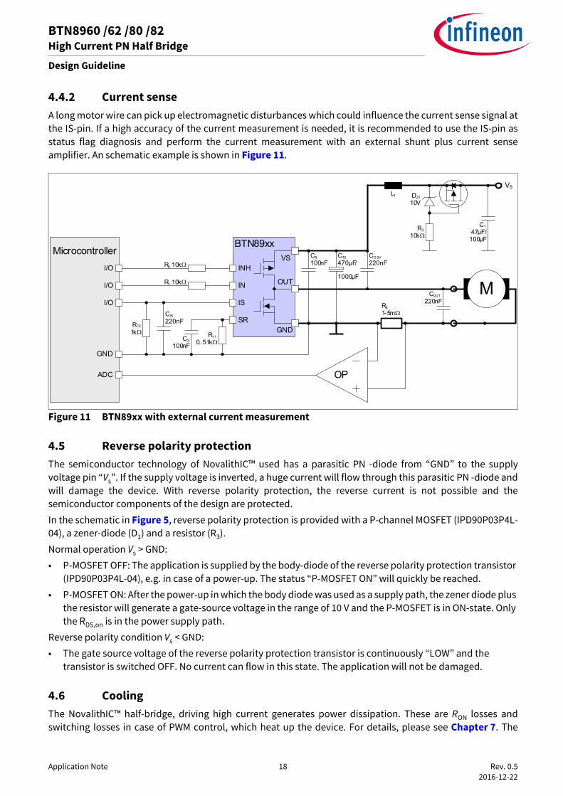
4.4.2 Current senseA long motor wire can pick up electromagnetic disturbances which could influence the current sense signal atthe IS-pin. If a high accuracy of the current measurement is needed, it is recommended to use the IS-pin asstatus flag diagnosis and perform the current measurement with an external shunt plus current senseamplifier. An schematic example is shown in Figure 11.
Figure 11 BTN89xx with external current measurement
4.5 Reverse polarity protectionThe semiconductor technology of NovalithIC™ used has a parasitic PN -diode from “GND” to the supplyvoltage pin “Vs”. If the supply voltage is inverted, a huge current will flow through this parasitic PN -diode andwill damage the device. With reverse polarity protection, the reverse current is not possible and thesemiconductor components of the design are protected. In the schematic in Figure 5, reverse polarity protection is provided with a P-channel MOSFET (IPD90P03P4L-04), a zener-diode (D1) and a resistor (R3). Normal operation Vs > GND:• P-MOSFET OFF: The application is supplied by the body-diode of the reverse polarity protection transistor
(IPD90P03P4L-04), e.g. in case of a power-up. The status “P-MOSFET ON” will quickly be reached. • P-MOSFET ON: After the power-up in which the body diode was used as a supply path, the zener diode plus
the resistor will generate a gate-source voltage in the range of 10 V and the P-MOSFET is in ON-state. Only the RDS,on is in the power supply path.
Reverse polarity condition Vs < GND:• The gate source voltage of the reverse polarity protection transistor is continuously “LOW” and the
transistor is switched OFF. No current can flow in this state. The application will not be damaged.
4.6 CoolingThe NovalithIC™ half-bridge, driving high current generates power dissipation. These are RON losses andswitching losses in case of PWM control, which heat up the device. For details, please see Chapter 7. The
M
VS
Microcontroller C9
100nFC10
470µF/
R3
10kΩ
DZ1
10V
R1 10kΩ
R2 10kΩ
R11
0..51kΩ
R12
1kΩ
I/O
I/O
I/OCIS
220nF
CO 2V
220nF
C1
47µF/100µF
L1
INH
IN
IS
SR
BTN89xxVS
OUT
GND
COUT
220nF
C2
100nF
1000µF
ADC
GND
RS
1-5mΩ
OP

Application Note 19 Rev. 0.5 2016-12-22
BTN8960 /62 /80 /82High Current PN Half Bridge
Design Guideline
package PG-TO263-7-1 provides a low thermal resistance which can be combined with a heat sink on the PCBto avoid exceeding the absolute maximum temperature values of the data sheet. In Figure 6 a cooling area (brown top layer, where the NovalithIC™-OUT is connected) has already been drawn.Depending on the power dissipation, other thermal sources on the PCB and the ambient temperature, thecooling needs to be carefully adapted to each application. In addition the reverse polarity protection transistor T1 (Figure 5 and Figure 6) generates RDS,on power lossesand the cooling concept for this transistor must ensure that the device does not exceed the absolutemaximum junction temperature.

Application Note 20 Rev. 0.5 2016-12-22
BTN8960 /62 /80 /82High Current PN Half Bridge
Current Sense Improvement
5 Current Sense ImprovementThe NovalithICTM half-bridge-family has a current sense function with an IS-pin which provides the outputcurrent divided by a factor, so called dkILIS. The precision of the current measurement could be significantlyimproved by eliminating the IS-offset, dkILIS-production spread and respecting the temperature dependencyof the dkILIS.The table below provides an overview of possible combinations of procedures to reduce currentmeasurement errors.
5.1 Characteristic of the dkILIS The dkILIS has characteristic dependencies. The most important ones with respect to the supply voltage Vs andwith respect to the temperature, are described in this chapter.
5.1.1 Supply voltage dependency of dkILIS
The dependency of the dkILIS of the supply voltage Vs is negligible, as Figure 12 shows. This means the supplyvoltage can be ignored when calculating the load current.
Table 1 Current sense procedure and benefitsProcedures Load current
toleranceOffset compensation ±28%
Offset compensation Device dkILIS measurement
±10%
Offset compensation Device dkILIS measurement
Temperature estimation ±6%
Offset compensation Device dkILIS measurement
Temperature compensation ±3%

Application Note 21 Rev. 0.5 2016-12-22
BTN8960 /62 /80 /82High Current PN Half Bridge
Current Sense Improvement
Figure 12 dkILIS vs. the supply voltage Vs
5.1.2 TC 1000 life time testsLife time tests of 1000 hours with a dedicated device stress set up and with many devices from differentproduction lots showed the dkILIS is decreasing over life time up to -3%.
5.1.3 Temperature drift of the dkILIS
Figure 13 and Figure 14 show the characteristics of the dkILIS vs. temperature and production spread with ascaling at 25°C, including a series of lab measurement points for one device.

Application Note 22 Rev. 0.5 2016-12-22
BTN8960 /62 /80 /82High Current PN Half Bridge
Current Sense Improvement
Figure 13 BTN8960 /62 dkILIS vs. temperature
The function f(T) is dependent on the temperature coefficient of the shunt resistance in the control chip (a),the temperature coefficient of the shunt (b) and DT = T - 25 °C.
dkIL
IS(T
)/dk I
LIS(
25°C
)

Application Note 23 Rev. 0.5 2016-12-22
BTN8960 /62 /80 /82High Current PN Half Bridge
Current Sense Improvement
Figure 14 BTN8980 /82 dkILIS vs. temperature
The function f(T) is dependent on the temperature coefficient of the shunt resistance in the control chip (a),the temperature coefficient of the shunt (b) and DT = T - 25 °C.
5.2 Offset compensationThe BTN89xy series is featured with an artificial offset current at the IS-pin. This is shown in Figure 15.
dkIL
IS(T
)/dk I
LIS(
25°C
)

Application Note 24 Rev. 0.5 2016-12-22
BTN8960 /62 /80 /82High Current PN Half Bridge
Current Sense Improvement
Figure 15 IS-Pin Internal Structure
With this structure, it is possible to always have a measurable offset at IS without a load current. This makes iteasy to measure the offset with the microcontroller, store the offset value and process this in the currentmeasurement procedure. The offset must be compensated to allow a precise current measurement with the IS-pin. The offset should be compensated before activating the load. When an application such as a fuel pump runsconstantly with PWM, you can perform the offset compensation when INH=high and IN=low. In the PWM-phase, the best measurement results are achieved just before the rising edge of the IN-signal. With this procedure, the specified dkILIS of ±28% could be reached, even for small load currents. This includesproduction spread, temperature dependency and aging. Most errors are caused by production spread, whichcould be compensated by measuring of the dkILIS of each device (device-specific dkILIS). Details of thisapproach are described in the relevant chapter.
5.3 Device specific dkILIS
With a measurement of the offset current and one IS-value at a certain load current at 25 °C (e.g. 20 A), it ispossible to determine the individual dkILIS-device and store it permanently to the microcontroller of theapplication. With this value, the graphs in Figure 13 and in Figure 14 are valid. The extreme values areindicated by the blue line (+3sigma):• dkILIS-max-C = 1.08 (blue @ -40 °C)• dkILIS-min-H = 0.93 (blue @ 150 °C)Taking into account the aging of the device (see Chapter 5.1.2) the minimum value of Figure 13 andFigure 14 (blue line) must be reduced by 3% (multiplying 0.97). This means the extreme values are as follows: • dkILIS-max-C = 1.08 (blue @ -40 °C)• dkILIS-min-H-old = dkILIS-min-H * 0.97 = 0.9This could be assumed as an error of ±10% including temperature drift and aging.In this case, the typical value should be assumed as follows:• dkILIS-typ = 0.99The device calibration could be implemented in the module test sequence.
VS
RIS
IIS~ ILoad
ESD-ZD
VIS
Sense output logic
IS
IIS(lim)
IIS(offset)
Normal operation: current sense mode

Application Note 25 Rev. 0.5 2016-12-22
BTN8960 /62 /80 /82High Current PN Half Bridge
Current Sense Improvement
Figure 16 Generating the device fine dkILIS-device.
5.4 Device fine dkILIS and temperature compensationOn the other hand, the dkILIS is dependent on the temperature, which is shown in Figure 13 and Figure 14.These figures show a characteristic temperature drift with a low content of production spread. This makes itpossible to measure the temperature on the PCB and reduce the temperature dependency by means of acalculation in the microcontroller. This procedure is illustrated in Figure 17.
IOUT-0 = 0AIIS-0 = measured
(IIS-offset)
IOUT-20 = 20AIIS-20 = measured
dkILIS-device
= (IOUT-20 – IOUT-0)/(IIS-20 – IIS-0)
Device calibration
Application processing
ROMµC
(IL processing)IIS
IIS-0
IIS-20
IOUT-0 IOUT-20
IIS
IOUT
IOUT-mes
IIS
IOUT-mes
1 0% 10%

Application Note 26 Rev. 0.5 2016-12-22
BTN8960 /62 /80 /82High Current PN Half Bridge
Current Sense Improvement
Figure 17 Load current “IOUT” calculation with temperature compensation
Taking the extreme values from Figure 14:• dkILIS-max-C = 1.08 (blue @ -40 °C)• dkILIS-min-C = 1.05 (green @ -40 °C)• dkILIS-max-H = 0.955 (green @ 150 °C)• dkILIS-min-H = 0.925 (blue @ 150 °C)Multiplying the min. values with a factor of 0.97 (-3% aging) produces the following values: • dkILIS-max-C = 1.08 (blue @ -40 °C)• dkILIS-min-C-old = 1.0185 (green @ -40 °C)• dkILIS-max-H = 0.955 (green @ 150 °C)• dkILIS-min-H-old = 0.9 (blue @ 150 °C)Calculating the typical value for:• dkILIS-typ-C = 1.05• dkILIS-typ-H = 0.928These values could be compensated with a temperature measurement and the characteristic from Figure 13and Figure 14 to provide the value of dkILIS-typ = 1.
With this compensation, the new min. and max. values are: • dkILIS-max-C-T = 1.03 (blue @ -40 °C)• dkILIS-min-C-old-T = 0.9685 (green @ -40 °C)• dkILIS-max-H-T = 1.027 (green @ 150 °C)• dkILIS-min-H-old-T = 0.972 (blue @ 150 °C)
IOUT-0 = 0AIIS-0 = measured
(IIS-offset)
IOUT-20 = 20AIIS-20 = measured
dkILIS-device
= (IOUT-20 – IOUT-0)/(IIS-20 – IIS-0)
Production calibration
Application processing
Offset calibration
RAM
Temperature measurement
IIS-0
IIS-20
IOUT-0 IOUT-20
IIS
IOUT
ROMµC(IL processing)IIS
IOUT-mes
IIS
IOUT-mes
3% 3 %

Application Note 27 Rev. 0.5 2016-12-22
BTN8960 /62 /80 /82High Current PN Half Bridge
Current Sense Improvement
After temperature compensation, the min. and max. values are dkILIS-min-H-old-T and dkILIS-max-C-T.Ultimately, a current measurement with a precision of ±3% could be achieved!If higher tolerances are acceptable, the temperature measurement can be less precise.
5.4.1 An example of the IIS failure with a rough temperature estimationAssuming the dkILIS was calibrated during production at 25 °C, the IIS measurement failure could be reduced to±6%, only by estimating if the temperature is above or below 25 °C. This estimation could be done e.g. by usingthe temperature characteristic of the IIS-offset, which is included in the data sheet. Temperature below 25° C:• dkILIS-max-C = 1.08 (blue @ -40 °C)• dkILIS-min-25°C = 1Reducing the min. values with the -3% aging (multiplying with 0.97) the following values will be calculated: • dkILIS-max-C = 1.08 (blue @ -40 °C)• dkILIS-min-25°C-old = 0.97For temperatures above 25 °C the calculation method is essentially the same. Ultimately, a current measurement with a precision of ±6% could be achieved without any externaltemperature measurement!
5.5 IS-pin current sensing and fault detectionThe BTN89xy provides several additional sense and diagnosis functionalities, which will be explained here.
5.5.1 Current sensing concepts in applicationsIn comparison to its predecessor BTN79xy, the BTN89xy family's current sense output functionality has anadvanced feature. For illustration purposes, both the BTN7960 and the BTN8960 were deployed in the samehigh-side switching scenario, where an inductive load to ground was toggled with a duty cycle of 50%. Bothmeasurements were conducted with the Infineon “NovalithIC™ Demo Board V2.2”. The resultingmeasurements are shown in Figure 20 for the BTN7960 and in Figure 19 for the BTN8960. As described inFigure 15, both types have a similar behavior in the case of an error. Instead, their current sense functionalitydiffers in normal operating mode. While the BTN79xy blanks the IS output to 0A when the high-side MOSFETis switched off, the BTN89xy provides the offset current IIS(offset) instead. For monitoring purposes, the behavior of both the BTN79xy and the BTN89xy can be used for continuouscurrent monitoring, even in freewheeling mode: In bi-directional motor applications with two BTN98xy, thefreewheeling current can be monitored at the high-side MOSFET in forward direction. As shown in Figure 18,the freewheeling current IFW,HS can be observed with both high-side MOSFETs being closed. In the scenarioshown, the IS output of the left BTN89xy provides the current dependent signal, while the IFW,HS flows throughthe right BTN89xy in reverse direction.

Application Note 28 Rev. 0.5 2016-12-22
BTN8960 /62 /80 /82High Current PN Half Bridge
Current Sense Improvement
Figure 18 Two freewheeling path options for bi-directional motor applications, implemented with two BTN89xy.
5.5.1.1 BTN89xy - advanced current sense and fault diagnosisIn comparison to the BTN79xy, the BTN89xy does not mute the IS current sense output signal, which is alwayspresent. This results in the following behavior and additional diagnostic possibilities:• Offset compensation of IIS(offset):
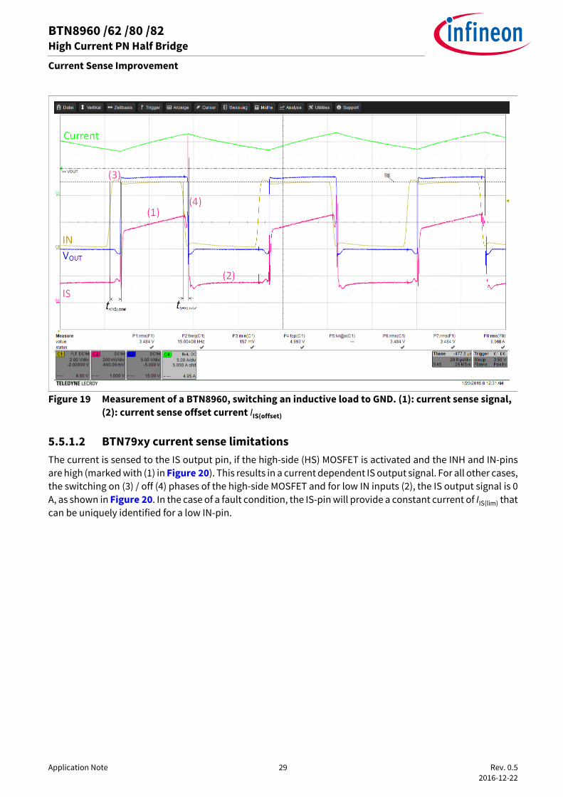
If no current is flowing through the high-side MOSFET, the current sense offset IIS(offset) can be monitored at the IS-pin. This can be ensured while the high-side switch is being switched off via the IN-pin and the freewheeling path doesn't go through the high-side MOSFET. If measured, this value can be used for an online offset calibration of IIS(offset), according to Chapter 5.2. In Figure 19 this scenario is marked with (2). In the case of a fault condition, the IS-pin will provide a constant current of IIS(lim), which can be clearly distinguished from the lower offset current IIS(offset).
• Online calibration of IIS(offset) and continuous current monitoring:If two BTN89xy devices are deployed in H-bridge configuration, the user can choose between either monitoring the freewheeling current or the online calibration of IIS(offset) by adapting the freewheeling path accordingly. An offset calibration of IIS(offset) for both the left and right BTN89xy can be carried out by choosing a freewheeling path through both low-side MOSFETs, with the freewheeling current IFW,LS displayed in Figure 18. As previously described, the current can be monitored continuously with a freewheeling current IFW,HS flowing through the two high-side MOSFETs.
VS
MINH
IN
IS
SR
BTN89xxVS
OUT
GND
VS
INH
IN
IS
SR
BTN89xxVS
OUT
GNDIFW,LS
IFW,HS
OFF ON ON OFF
Application Note 29 Rev. 0.5 2016-12-22
BTN8960 /62 /80 /82High Current PN Half Bridge
Current Sense Improvement
Figure 19 Measurement of a BTN8960, switching an inductive load to GND. (1): current sense signal, (2): current sense offset current IIS(offset)
5.5.1.2 BTN79xy current sense limitationsThe current is sensed to the IS output pin, if the high-side (HS) MOSFET is activated and the INH and IN-pinsare high (marked with (1) in Figure 20). This results in a current dependent IS output signal. For all other cases,the switching on (3) / off (4) phases of the high-side MOSFET and for low IN inputs (2), the IS output signal is 0A, as shown in Figure 20. In the case of a fault condition, the IS-pin will provide a constant current of IIS(lim) thatcan be uniquely identified for a low IN-pin.

Application Note 30 Rev. 0.5 2016-12-22
BTN8960 /62 /80 /82High Current PN Half Bridge
Current Sense Improvement
Figure 20 Measurement of a BTN7960, switching an inductive load to GND. (1): current sense signal, (2): current sense functionality switched off
5.5.2 Fault detectionThe current sense accuracy depends on the spread of the two parameters dkILIS and IIS(offset). The resultingmaximal, typical and minimal behavior is displayed in Figure 21 for the BTN8960/62 and in Figure 22 for theBTN8980/82. Here, the limits for the sense current in fault condition IIS(lim) are also shown.

Application Note 31 Rev. 0.5 2016-12-22
BTN8960 /62 /80 /82High Current PN Half Bridge
Current Sense Improvement
Figure 21 Behavior of the BTN8960/62’s IS output pin for current sense and fault condition according to parameter tolerances
Figure 22 Behavior of the BTN8980/82’s IS output pin for current sense and fault condition according to parameter tolerances
The possibility to distinguish whether a current sense signal or the constant sense current IIS(lim), indicating afault condition, can be measured at the IS-pin is also an important issue. Therefore the fault distance betweenthe two states is further considered. The combined (possible) output options for both states can be seen inFigure 21 for the BTN8960/62 and in Figure 22 for the BTN8980/82. For a worst case combination of the threeparameters IIS(lim), dkILIS and IIS(offset), provided in the data sheet for the given tolerances, there is a currentrange, where it is not possible to distinguish the right operation mode, whether there is a fault or not.
0 5 10 15 20 25 300
1
2
3
4
5
6
7
IL − load current (A)
IS (
mA
)
max. IIS(lim)
typ. IIS(lim)
min. IIS(lim)
max. IS typ. IS min. IS
0 5 10 15 20 25 30 35 40 45 50 550
1
2
3
4
5
6
7
IL − load current (A)
IS (
mA
)
max. IIS(lim)
typ. IIS(lim)
min. IIS(lim)
max. IS typ. IS min. IS

Application Note 32 Rev. 0.5 2016-12-22
BTN8960 /62 /80 /82High Current PN Half Bridge
Current Sense Improvement
The corresponding break-even point for the BTN8960/62 can be calculated for the load current IL accordingly:
(5.1)
(5.2)
For such a system, it wouldn’t be possible to distinguish easily between the fault condition current IIS(lim) anda current sense signal, for IL > 25 A if the BTN8960/62 is used, and IL > 50 A for the BTN8980/82. For a moreprecise consideration, also the temperature dependency of IIS(lim), dkILIS and IIS(offset) has to be considered. Forthe given critical area for load currents IL > 25 A, especially the parameters dkILIS and IIS(lim) have the greatestinfluence. The temperature dependency of dkILIS is described in Chapter 5.1.3, and of IIS(lim) inChapter 5.5.2.1:• For a rising temperature, the fault condition current IIS(lim) increases, and vice versa.• For a rising temperature the dkILIS decreases and vice versa.This relationship is also illustrated by Figure 23.
Figure 23 Illustration of the temperature dependencies of the fault distance and relevant parameters
Additionally the difference between the fault condition current IIS(lim) and the sensed current IIS(IL) can becalculated as follows:
(5.3)
Equation (5.3) shows, that for a rising temperature, both IIS(lim) and IIS(IL) (due to IL / dkILIS) increase.
IIS
load current - IL
IIS(lim)
IIS(lim)
30A
rising temperature
∆IIS
∆IIS
IIS(lim)
dkILIS
cold
hot

Application Note 33 Rev. 0.5 2016-12-22
BTN8960 /62 /80 /82High Current PN Half Bridge
Current Sense Improvement
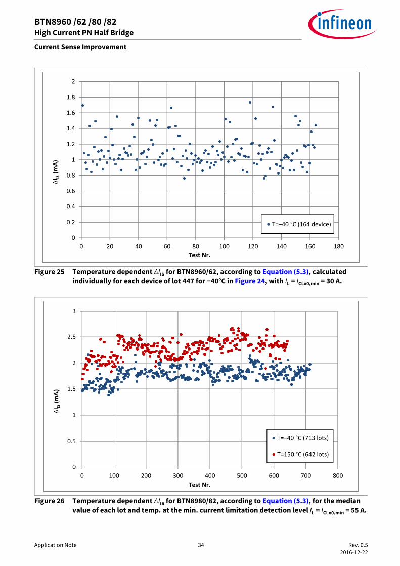
Combining the spread of dkILIS and IIS(lim) over temperature, this behavior results in a ∆IISthat, at the min.current limitation detection level ICLx0,min, is typically above 0,5 mA for the BTN8960/62, as shown in Figure 24and Figure 25 and above 0,75 mA for the BTN8980/82, shown in Figure 26 and Figure 27. To summarize, wecan say that it is possible to distinguish between a current sense signal IIS(IL) and a fault condition current IIS(lim)for any temperature.
Figure 24 Temperature dependent ∆IIS for BTN8960/62, according to Equation (5.3), for the median value of each lot and temperature at the min. current limitation detection level IL = ICLx0,min = 30 A.
0
0.5
1
1.5
2
2.5
3
0 50 100 150 200 250 300 350 400 450 500
∆IIS
(mA)
Test Nr.
T=−40 °C (456 lots)
T=150 °C (425 lots)
Application Note 34 Rev. 0.5 2016-12-22
BTN8960 /62 /80 /82High Current PN Half Bridge
Current Sense Improvement
Figure 25 Temperature dependent ∆IIS for BTN8960/62, according to Equation (5.3), calculated individually for each device of lot 447 for −40°C in Figure 24, with IL = ICLx0,min = 30 A.
Figure 26 Temperature dependent ∆IIS for BTN8980/82, according to Equation (5.3), for the median value of each lot and temp. at the min. current limitation detection level IL = ICLx0,min = 55 A.
0
0.2
0.4
0.6
0.8
1
1.2
1.4
1.6
1.8
2
0 20 40 60 80 100 120 140 160 180
∆IIS
(mA)
Test Nr.
T=−40 °C (164 device)
0
0.5
1
1.5
2
2.5
3
0 100 200 300 400 500 600 700 800
∆IIS
(mA)
Test Nr.
T=−40 °C (713 lots)
T=150 °C (642 lots)
Application Note 35 Rev. 0.5 2016-12-22
BTN8960 /62 /80 /82High Current PN Half Bridge
Current Sense Improvement
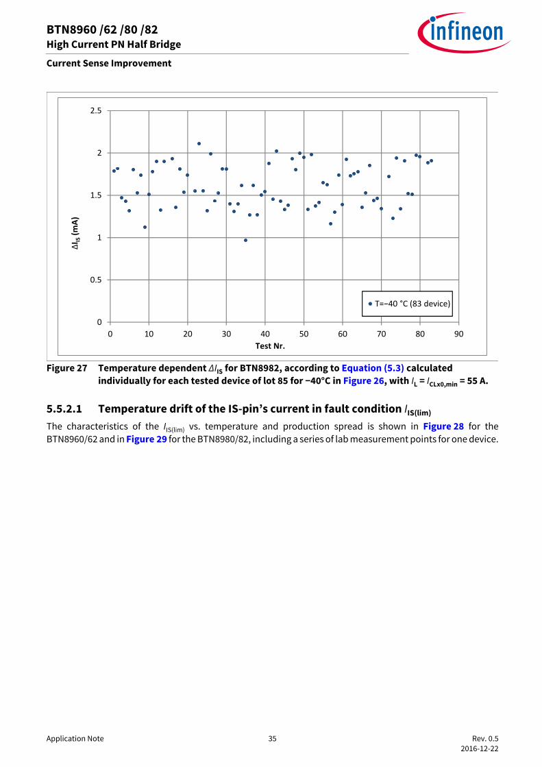
Figure 27 Temperature dependent ∆IIS for BTN8982, according to Equation (5.3) calculated individually for each tested device of lot 85 for −40°C in Figure 26, with IL = ICLx0,min = 55 A.
5.5.2.1 Temperature drift of the IS-pin’s current in fault condition IIS(lim)
The characteristics of the IIS(lim) vs. temperature and production spread is shown in Figure 28 for theBTN8960/62 and in Figure 29 for the BTN8980/82, including a series of lab measurement points for one device.
0
0.5
1
1.5
2
2.5
0 10 20 30 40 50 60 70 80 90
∆IIS
(mA)
Test Nr.
T=−40 °C (83 device)

Application Note 36 Rev. 0.5 2016-12-22
BTN8960 /62 /80 /82High Current PN Half Bridge
Current Sense Improvement
Figure 28 BTN8960/62 IIS(lim) vs. temperature
Figure 29 BTN8980/82 IIS(lim) vs. temperature
4
4.5
5
5.5
6
6.5
7
-60 -40 -20 0 20 40 60 80 100 120 140 160
I IS(li
m)(
mA)
T (°C)
Lab
f(T) = a + b·T
f(-40) 456 lots
f(150) 425 lots
+ 3σ
- 3σ
a = 4.87b = 4.3· 10-03
4
4.5
5
5.5
6
6.5
7
-60 -40 -20 0 20 40 60 80 100 120 140 160
I IS(li
m)(
mA)
T (°C)
Lab
f(T) = a + b·T
f(-40) 630 lots
f(150) 579 lots
+ 3σ
- 3σ
a = 4.78b = 4.1· 10-03

Application Note 37 Rev. 0.5 2016-12-22
BTN8960 /62 /80 /82High Current PN Half Bridge
Current Sense Improvement
5.5.2.2 Failure detection flow chart The consideration of ∆IIS above provides a procedure for detecting fault conditions (IIS(lim)), which is alsosummarized in Figure 30:• Calibration of IIS(lim)(T0) for a specific temperature T0: Calculation of offset a with the given / typical slope b.
Ideally measurement of IIS(lim)(T1) for a second temperature T1, to perform a two point calibration and calculate both offset a and slope b for each individual device.
• Calculation of temperature dependent IIS(lim)(T) = f(T) while the device is operating according to Chapter 5.5.2.1.
• If a current limit of IIS = IIS(lim)(T) - 0,5 mA is exceeded, a fault condition is detected.
Figure 30 One point calibration of IIS(lim) and the resulting fault detection level over temperature for the BTN8960/62
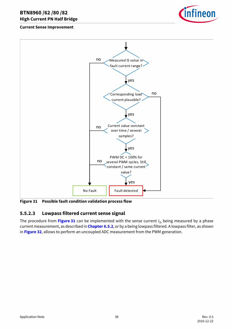
Additional measures are available for ascertaining fault conditions. Figure 31 describes a possible procedure.Carrying out a plausibility check after detecting a potential fault allows you to determine if a specific loadcurrent value in the current range of IIS(lim) is possible at a specific operating point.If this is the case, check whether that value stays in a certain range by performing a series of measurements.Depending on the application, the scattering of the current sense signal of an electric motor should be muchhigher than that of the constant fault current. An additional way of validating a fault condition is by measuringthe IS output pin for a low IN input pin. As illustrated in Figure 18, the fault condition can be monitored bychoosing the low-side freewheeling path, ensuring that no current is flowing through the high-side MOSFETs.The fault condition current IIS(lim) can be clearly distinguished from the lower offset current IIS(offset). Forapplications running with a PWM duty cycle of 100%, the duty cycle must be reduced for certain cycles in orderto validate a fault condition. This fault detection procedure is summarized in Figure 31.
3
3.5
4
4.5
5
5.5
6
6.5
7
-60 -40 -20 0 20 40 60 80 100 120 140 160
I IS(li
m)(m
A)
T (°C)
Calibration (25°C)
f(T) = a + b·T
f(T) – 0,5 mA
a = 4.69b = 4.3· 10-03
0,5 mA
Application Note 38 Rev. 0.5 2016-12-22
BTN8960 /62 /80 /82High Current PN Half Bridge
Current Sense Improvement
Figure 31 Possible fault condition validation process flow
5.5.2.3 Lowpass filtered current sense signalThe procedure from Figure 31 can be implemented with the sense current IIS being measured by a phasecurrent measurement, as described in Chapter 6.5.2, or by a being lowpass filtered. A lowpass filter, as shownin Figure 32, allows to perform an uncoupled ADC measurement from the PWM generation.
PWM DC < 100% for several PWM cycles. Still constant / same current
value?
Corresponding load current plausible?
Measured IS value in fault current range?
Fault detected
no
yes
yes
No Fault
yes
no
no
yes
Current value constant over time / several
samples?
no

Application Note 39 Rev. 0.5 2016-12-22
BTN8960 /62 /80 /82High Current PN Half Bridge
Current Sense Improvement
Figure 32 Application circuit including a lowpass filtered current sense signal for a monodirectional motor with BTN89xy
The fault distance increases here for a decreasing (effective) duty cycle DC (for a low-side freewheeling path).The average lowpass filtered IIS signal can be estimated to:
(5.4)
Based on a measured lowpass filtered voltage VLP the load current IL can now be estimated as follows:
(5.5)
While the fault current is constant at IIS(lim). A possible scenario is shown in Figure 33. Here, a load to groundwas simulated. By changing the duty cycle for some periods, the lowpass filtered current sense signal shouldfurther decrease thus increasing the fault distance, as the average Motor current decreases and the timeduring which only the lower offset current is provided by the IS-pin increases.Another way for fault detection is comparing the lowpass filtered signal VLP with the IIS / VIS signal. As shown inFigure 33, the IIS / VIS signal, with VIS = IS · R12, is above VLP during the PWM’s ON-phases and with IIS= IIS(offset)below VLP during the OFF-phase. By comparing the two signals (VIS and VLP), a constant fault signal IIS(lim) canbe detected, as their are only transitions during normal operation.
M
XC866
TLE 4278G
VS
I/O
Reset
Vdd
Vss
WO
RO
Q
D GND
I
Microcontroller Reverse Polarity Protection
(IPD 90P03P4L-04)
Voltage Regulator
C9
100nF
CD
47nF
CQ
22µF
C10
470µF
R3
10kΩ
DZ1
10V
R1
10kΩ
R2
10kΩ
R11
0..51kΩ
R12
1kΩ
I/OI/OI/O
CI
470nF
CIS
1nF
CO2 V
220nF
C1
100nF
L1
COUT
220nF
C2
100nF
INH
IN
IS
SR
VS
OUT
GND
BTN89xx
RLP
20kΩ
CLP
5nF
I/O
VLP VIS
IIS

Application Note 40 Rev. 0.5 2016-12-22
BTN8960 /62 /80 /82High Current PN Half Bridge
Current Sense Improvement
Figure 33 BTN8982TA simulation: Lowpass-filtered (RLP = 20 kΩ; CLP = 5 nF; R12 = 1 kΩ) current sense signal IIS for ADC measurement with the fault condition current IIS(lim) from 350 µs. PWM operation (20 kHz; DC = 90%) with load to ground.
0
1
2
3
4
5
6
0.00
1.00
2.00
3.00
4.00
5.00
6.00
0 100 200 300 400 500 600 700
Curr
ent I
IS(m
A)
Volta
ge V
LP/
V IS
(V)
Time (µs)
V_LP
I_IS /~V_IS
overtemperature
VLPIIS / ~VIS

Application Note 41 Rev. 0.5 2016-12-22
BTN8960 /62 /80 /82High Current PN Half Bridge
Switching Timing
6 Switching TimingFor the ADC measurement of the IS-pin, the timing behavior of the BTN89xy needs to be considered. As thecurrent sense output is proportional to the current through the high-side switch, only the high-side switchbehavior is considered here exemplary. The behavior of the low-side switch can be considered in an equalfashion. An overview of the rising and falling switching procedure is shown in Figure 34.
Figure 34 Timing behavior overview of a BTNx9yz high-side switch
As shown in the data sheet, the time between the IN-pin rising from a 0 to 1 corresponding voltage level andthe BTN89xy output voltage rising from (around) 0 V to 80 % of the final output voltage (typically: VOUT ≈ VS) canbe summed up to the following delay, as shown in Figure 34:
(6.1)
For a falling edge on the IN input pin, the delay time between the falling edge of the IN input pin and the lowerdeviation of 20% of the VOUT ≈ VS voltage level of the output pin OUT is considered:
(6.2)
The timings and slew rates of the power switches can be adjusted by connecting a resistor RSR between the SR-pin and GND-pin of the device. An overview about the, in this document provided, dependencies of the chosenresistor value RSR on relevant timings is given in Table 2.In the following two subchapter, the BTN8982TA is described in Chapter 6.1 and the BTN8962TA inChapter 6.2.
IN
VOUT
t
t
ΔVOUT
tdr (HS )
tr(HS )
tdf (HS)
tf (HS)
ΔVOUT
20% 20%
80%80%
tr(HS ),total t f(HS),total

Application Note 42 Rev. 0.5 2016-12-22
BTN8960 /62 /80 /82High Current PN Half Bridge
Switching Timing
Table 2 Overview about the dynamic characteristic plots for BTN8982TA and BTN8982TA(RSR dependency)
Pos. (in Data Sheet)1)
1) BTN8982TA/BTN8962TA Data Sheet, Rev. 1.0, 2013-05-17
Parameter Symbol Figure for BTN8982TA
Figure for BTN8962TA
High Side Switch
5.2.7 Rise-Time of HS tr(HS) Figure 35 Figure 45 5.2.8 Switch ON Delay Time HS tdr(HS) Figure 36 Figure 46 tr(HS)+ tdr(HS) tr(HS),total Figure 37 Figure 47 5.2.9 Fall-Time of HS tf(HS) Figure 38 Figure 48 5.2.10 Switch OFF Delay Time HS tdf(HS) Figure 39 Figure 49 tf(HS)+ tdf(HS) tf(HS),total Figure 40 Figure 50 Low Side Switch
5.2.11 Rise-Time of LS tr(LS) Figure 41 Figure 51 5.2.12 Switch OFF Delay Time LS tdr(LS) Figure 42 Figure 52 5.2.13 Fall-Time of HS tf(LS) Figure 43 Figure 53 5.2.14 Switch ON Delay Time LS tdf(LS) Figure 44 Figure 54

Application Note 43 Rev. 0.5 2016-12-22
BTN8960 /62 /80 /82High Current PN Half Bridge
Switching Timing
6.1 BTN8982TAUnless otherwise specified, the times are specified for VS = 13,5 V, Rload = 2 Ω, 30 µH < Lload < 40 µH (in series toRload) and single pulse.
6.1.1 Timing behavior for rising edge on high-side switch
Figure 35 tr(HS): Dependency of the slew rate resistor RSR on the rise-time of the high-side switch of BTN8982TA
Figure 36 tdr(HS): Dependency of the slew rate resistor RSR on the switch ON delay time of the high-side switch of BTN8982TA
0 5 10 15 20 25 30 35 40 45 500
0.5
1
1.5
2
2.5
RSR
(kΩ)
t r(H
S) −
ris
e−tim
e H
S (
μs)
+ 6σ typ. − 6σ
0 5 10 15 20 25 30 35 40 45 500
5
10
15
20
RSR
(kΩ)
t dr(H
S) −
Sw
itch
ON
Del
ay T
ime
HS
(μs)
+ 6σ typ. − 6σ

Application Note 44 Rev. 0.5 2016-12-22
BTN8960 /62 /80 /82High Current PN Half Bridge
Switching Timing
Figure 37 Dependency of the slew rate resistor RSR on the total rise time of the high-side switch with tr(HS),total = tr(HS) + tdr(HS): BTN8982TA
6.1.2 Timing behavior for falling edge on high-side switch
Figure 38 tf(HS): Dependency of the slew rate resistor RSR on the fall-time of the high-side switch of BTN8982TA
0 5 10 15 20 25 30 35 40 45 500
5
10
15
20
RSR
(kΩ)
t r(H
S),
tota
l − to
tal r
isin
g−tim
e H
SS
(μs
)
+ 6σ typ. − 6σ
0 5 10 15 20 25 30 35 40 45 500
0.2
0.4
0.6
0.8
1
1.2
1.4
1.6
1.8
2
RSR
(kΩ)
t f(H
S) −
fall−
time
HS
(μs)
+ 6σ typ. − 6σ

Application Note 45 Rev. 0.5 2016-12-22
BTN8960 /62 /80 /82High Current PN Half Bridge
Switching Timing
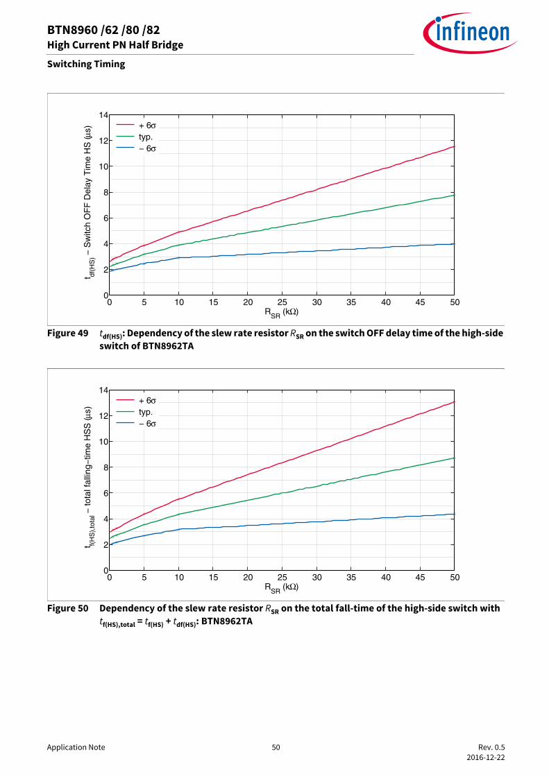
Figure 39 tdf(HS): Dependency of the slew rate resistor RSR on the switch OFF delay time of the high-side switch of BTN8982TA
Figure 40 Dependency of the slew rate resistor RSR on the total fall time of the high-side switch with tf(HS),total = tf(HS) + tdf(HS): BTN8982TA
0 5 10 15 20 25 30 35 40 45 500
2
4
6
8
10
12
14
16
18
RSR
(kΩ)
t df(H
S) −
Sw
itch
OF
F D
elay
Tim
e H
S (μ
s)
+ 6σ typ. − 6σ
0 5 10 15 20 25 30 35 40 45 500
2
4
6
8
10
12
14
16
18
RSR
(kΩ)
t f(H
S),
tota
l − to
tal f
allin
g−tim
e H
SS
(μs)
+ 6σ typ. − 6σ
Application Note 46 Rev. 0.5 2016-12-22
BTN8960 /62 /80 /82High Current PN Half Bridge
Switching Timing
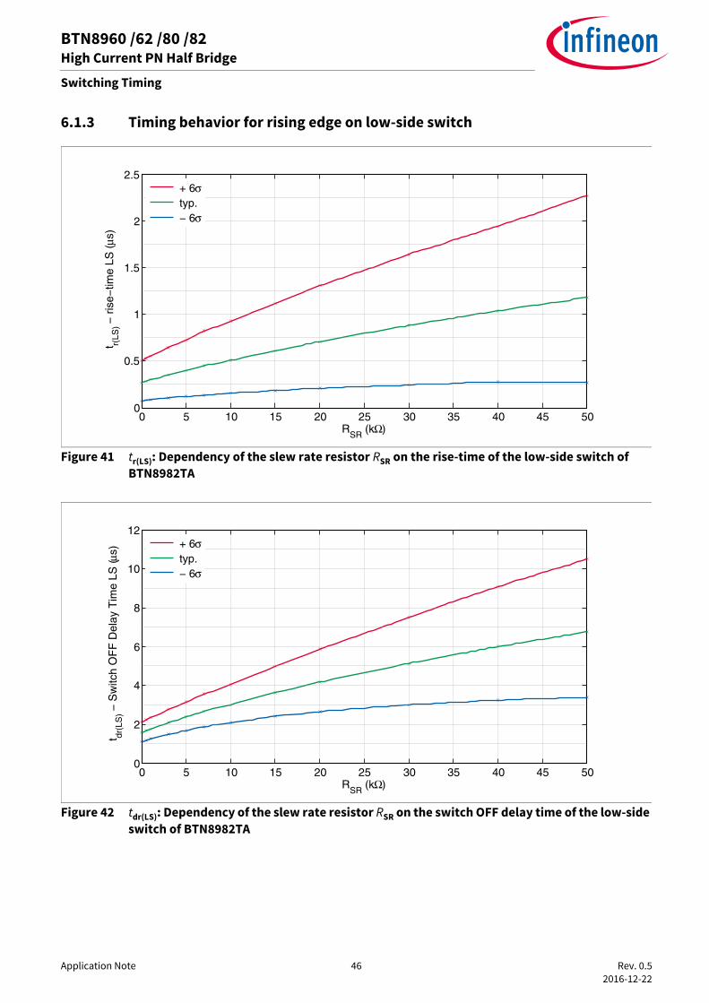
6.1.3 Timing behavior for rising edge on low-side switch
Figure 41 tr(LS): Dependency of the slew rate resistor RSR on the rise-time of the low-side switch of BTN8982TA
Figure 42 tdr(LS): Dependency of the slew rate resistor RSR on the switch OFF delay time of the low-side switch of BTN8982TA
0 5 10 15 20 25 30 35 40 45 500
0.5
1
1.5
2
2.5
RSR
(kΩ)
t r(LS
) − r
ise−
time
LS (μ
s)
+ 6σ typ. − 6σ
0 5 10 15 20 25 30 35 40 45 500
2
4
6
8
10
12
RSR
(kΩ)
t dr(L
S) −
Sw
itch
OF
F D
elay
Tim
e LS
(μs)
+ 6σ typ. − 6σ

Application Note 47 Rev. 0.5 2016-12-22
BTN8960 /62 /80 /82High Current PN Half Bridge
Switching Timing
6.1.4 Timing behavior for falling edge on low-side switch
Figure 43 tf(LS): Dependency of the slew rate resistor RSR on the fall-time of the low-side switch of BTN8982TA
Figure 44 tdf(LS): Dependency of the slew rate resistor RSR on the switch ON delay time of the low-side switch of BTN8982TA
0 5 10 15 20 25 30 35 40 45 500
0.5
1
1.5
2
2.5
RSR
(kΩ)
t f(LS
) − fa
ll−tim
e LS
(μs)
+ 6σ typ. − 6σ
0 5 10 15 20 25 30 35 40 45 50
5
10
15
20
25
RSR
(kΩ)
t df(L
S) −
Sw
itch
ON
Del
ay T
ime
LS (μ
s)
+ 6σ typ. − 6σ

Application Note 48 Rev. 0.5 2016-12-22
BTN8960 /62 /80 /82High Current PN Half Bridge
Switching Timing
6.2 BTN8962TAUnless otherwise specified, the times are specified for VS = 13,5 V, Rload = 2 Ω, 30 µH < Lload < 40 µH (in series toRload) and single pulse.
6.2.1 Timing behavior for rising edge on high-side switch
Figure 45 tr(HS): Dependency of the slew rate resistor RSR on the rise-time of the high-side switch of BTN8962TA
Figure 46 tdr(HS): Dependency of the slew rate resistor RSR on the switch ON delay time of the high-side switch of BTN8962TA
0 5 10 15 20 25 30 35 40 45 500
0.2
0.4
0.6
0.8
1
1.2
1.4
1.6
1.8
RSR
(kΩ)
t r(H
S) −
ris
e−tim
e H
S (
μs)
+ 6σ typ. − 6σ
0 5 10 15 20 25 30 35 40 45 500
2
4
6
8
10
12
14
16
RSR
(kΩ)
t dr(H
S) −
Sw
itch
ON
Del
ay T
ime
HS
(μs)
+ 6σ typ. − 6σ
Application Note 49 Rev. 0.5 2016-12-22
BTN8960 /62 /80 /82High Current PN Half Bridge
Switching Timing
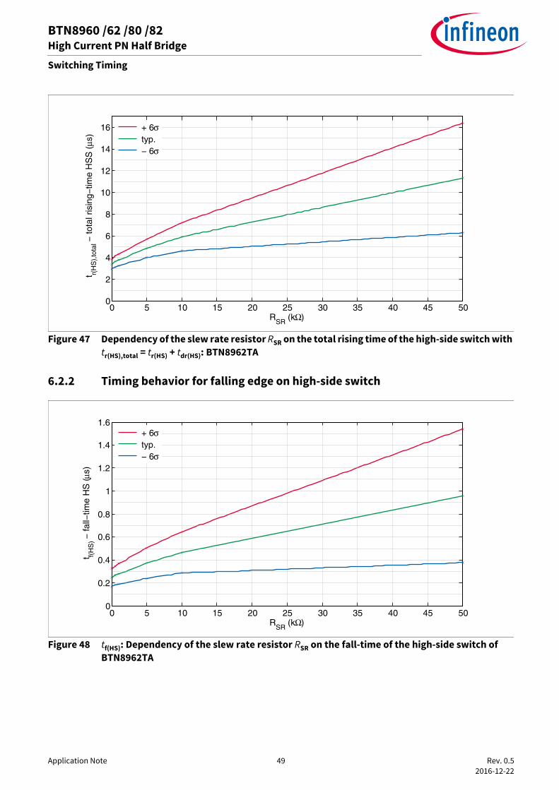
Figure 47 Dependency of the slew rate resistor RSR on the total rising time of the high-side switch with tr(HS),total = tr(HS) + tdr(HS): BTN8962TA
6.2.2 Timing behavior for falling edge on high-side switch
Figure 48 tf(HS): Dependency of the slew rate resistor RSR on the fall-time of the high-side switch of BTN8962TA
0 5 10 15 20 25 30 35 40 45 500
2
4
6
8
10
12
14
16
RSR
(kΩ)
t r(H
S),
tota
l − to
tal r
isin
g−tim
e H
SS
(μs
)
+ 6σ typ. − 6σ
0 5 10 15 20 25 30 35 40 45 500
0.2
0.4
0.6
0.8
1
1.2
1.4
1.6
RSR
(kΩ)
t f(H
S) −
fall−
time
HS
(μs)
+ 6σ typ. − 6σ
Application Note 50 Rev. 0.5 2016-12-22
BTN8960 /62 /80 /82High Current PN Half Bridge
Switching Timing
Figure 49 tdf(HS): Dependency of the slew rate resistor RSR on the switch OFF delay time of the high-side switch of BTN8962TA
Figure 50 Dependency of the slew rate resistor RSR on the total fall-time of the high-side switch with tf(HS),total = tf(HS) + tdf(HS): BTN8962TA
0 5 10 15 20 25 30 35 40 45 500
2
4
6
8
10
12
14
RSR
(kΩ)
t df(H
S) −
Sw
itch
OF
F D
elay
Tim
e H
S (μ
s)
+ 6σ typ. − 6σ
0 5 10 15 20 25 30 35 40 45 500
2
4
6
8
10
12
14
RSR
(kΩ)
t f(H
S),
tota
l − to
tal f
allin
g−tim
e H
SS
(μs)
+ 6σ typ. − 6σ

Application Note 51 Rev. 0.5 2016-12-22
BTN8960 /62 /80 /82High Current PN Half Bridge
Switching Timing
6.2.3 Timing behavior for rising edge on low-side switch
Figure 51 tr(LS): Dependency of the slew rate resistor RSR on the rise-time of the low-side switch of BTN8962TA
Figure 52 tdr(LS): Dependency of the slew rate resistor RSR on the switch OFF delay time of the low-side switch of BTN8962TA
0 5 10 15 20 25 30 35 40 45 500
0.2
0.4
0.6
0.8
1
1.2
1.4
1.6
1.8
RSR
(kΩ)
t r(LS
) − r
ise−
time
LS (μ
s)
+ 6σ typ. − 6σ
0 5 10 15 20 25 30 35 40 45 500
1
2
3
4
5
6
7
8
9
RSR
(kΩ)
t dr(L
S) −
Sw
itch
OF
F D
elay
Tim
e LS
(μs)
+ 6σ typ. − 6σ

Application Note 52 Rev. 0.5 2016-12-22
BTN8960 /62 /80 /82High Current PN Half Bridge
Switching Timing
6.2.4 Timing behavior for falling edge on low-side switch
Figure 53 tf(LS): Dependency of the slew rate resistor RSR on the fall-time of the low-side switch of BTN8962TA
Figure 54 tdf(LS): Dependency of the slew rate resistor RSR on the switch ON delay time of the low-side switch of BTN8962TA
6.3 Error of total delay timeThe resulting relative error for the ±6σ values, compared to the typical tx(HS),total value, is summarized inFigure 55 (BTN8962TA) / Figure 56 (BTN8982TA). The error is calculated as follows:
(6.3)
0 5 10 15 20 25 30 35 40 45 500
0.2
0.4
0.6
0.8
1
1.2
1.4
1.6
1.8
RSR
(kΩ)
t f(LS
) − fa
ll−tim
e LS
(μs)
+ 6σ typ. − 6σ
0 5 10 15 20 25 30 35 40 45 502
4
6
8
10
12
14
16
18
20
RSR
(kΩ)
t df(L
S) −
Sw
itch
ON
Del
ay T
ime
LS (μ
s)
+ 6σ typ. − 6σ

Application Note 53 Rev. 0.5 2016-12-22
BTN8960 /62 /80 /82High Current PN Half Bridge
Switching Timing
This parameter spread needs to be taken into account especially for short PWM cycle times, respectively highPWM frequencies. If the relative tr(HS),total / tf(HS),total error is in the same order of magnitude as the application’sPWM cycle time, a separate calibration can be considered to measure the delay times of the individual BTx9yzdevices.
Figure 55 Relative error of the total delay time tr(HS),total for rising and tf(HS),total for falling edges. Relative error according to Equation (6.3) for BTN8962TA (VS = 13,5 V, Rload = 2 Ω 30 µH < Lload < 40 µH (in series to Rload), single pulse)
Figure 56 Relative error of the total delay time tr(HS),total for rising and tf(HS),total for falling edges.
0 5 10 15 20 25 30 35 40 45 50
−50
−40
−30
−20
−10
0
10
20
30
40
50
RSR
(kΩ)
rel.
erro
r t x(
HS
)tot
al (
%)
6σ tf(HS)total
6σ tr(HS)total
−6σ tr(HS)total
−6σ tf(HS)total
0 5 10 15 20 25 30 35 40 45 50
−50
−40
−30
−20
−10
0
10
20
30
40
50
60
RSR
(kΩ)
rel.
erro
r t x(
HS
)tot
al (
%)
6σ tf(HS)total
6σ tr(HS)total
−6σ tr(HS)total
−6σ tf(HS)total

Application Note 54 Rev. 0.5 2016-12-22
BTN8960 /62 /80 /82High Current PN Half Bridge
Switching Timing
Relative error according to Equation (6.3) for BTN8982TA (VS = 13,5 V, Rload = 2 Ω 30 µH < Lload < 40 µH (in series to Rload), single pulse)
6.4 Delay time calibrationOne possibility to determine the total rising time tr(HS),total and the falling time tf(HS),total respectively, is bymeasuring the time once in an end of line test. For such a (single) measurement, the influence of certainparameters like the supply voltage or the load current has to be considered as well and the test setup has tobe adjusted accordingly.It is also possible to use continuous calibration during operation. With such a method, the influence ofchanging outside parameters is constantly taken into account.In the following two chapters, an output voltage (Chapter 6.4.1) and current sense based calibration(Chapter 6.4.2) is suggested.
6.4.1 Output voltage based calibrationThis method can be implemented if both the supply voltage VS and the BTN89xy’s output voltage VOUT at theOUT-pin are measured. In that case it would be possible to measure the time between setting the IN input pinfrom low to high (or from high to low for tf(HS),total) and the point of time, the output voltage VOUT is greater thanor equal to 0,8 VS. The measurement procedure is illustrated in Figure 57.The procedure for the total falling delay time tf(HS),total measurement can be performed in a similar fashion: thedelay time between the falling edge of the IN-pin and the lower deviation of 20% of the VOUT ≈ VS voltage levelis considered.If these two voltage levels are monitored during operation, an online calibration can be performedperiodically, too.
Figure 57 Measurement procedure for the total rising time tr(HS),total based on two voltage measurements
Event generation (Interrupt)
IN
VOUT
t
t
VS·80% Upper Boundary
Stop timer
Start timer
tr(HS),total

Application Note 55 Rev. 0.5 2016-12-22
BTN8960 /62 /80 /82High Current PN Half Bridge
Switching Timing
6.4.2 Current sense based calibrationTwo different calibration methods are available when only the current sense signal is monitored. One of thesecan be implemented as an end of line test, while the other is performed during live operation.
Figure 58 End of line test setup for timing calibration with ohmic load Rtest
To determine the delay for a rising edge tr(HS),total, the voltage limit is set to the corresponding current level,which is reached with a voltage drop of 80% of VOUT ≈ VS over the test resistor Rtest, as shown in the test setupin Figure 58. As this test is based on the concurrency of the output voltage and current IL, only an ohmic loadshould be used. This setup results in the direct proportional context of IL = VS ⁄ Rtest and with the current sensefunction from Chapter 5.5:
(6.4)
The resulting voltage VADC on the microcontroller’s ADC input pin (according to Figure 58):
(6.5)
This means that the comparator threshold should be set to a corresponding voltage level of:
(6.6)
XC866
TLE 4278G
VS
I/O
Reset
Vdd
Vss
WO
RO
Q
D GND
I
Microcontroller Reverse Polarity Protection
(IPD90P03P4L-04)
Voltage Regulator
C9
100nF
CD
47nF
CQ
22µF
C10
470µF
R3
10kΩ
DZ1
10V
R1
10kΩ
R2
10kΩ
R11
0..51kΩ
R12
1kΩ
I/OI/OI/O
CI
470nF
CIS
1nF
CO2V
220nF
C1
100nF
L1
COUT
220nF
C2
100nF
VS
OUT
INH
IN
IS
SRGND
BTN89xxTA
Rtest

Application Note 56 Rev. 0.5 2016-12-22
BTN8960 /62 /80 /82High Current PN Half Bridge
Switching Timing
This procedure allows to measure the input delay tr(HS),total with a microcontroller’s ADC in a predefined end ofline test, with a known resistor Rtest. The test is summarized in Figure 59. The time measurement is started inparallel to the rising edge of the IN input pin. If the voltage level of VADC, as described in Equation (6.6), isreached, the resulting delay time tr(HS),total can be calculated.
Figure 59 Measurement procedure for the total rising time tr(HS),total based on a current sense measurement
This procedure, which is described here for a rising edge, can be implemented in a similar manner to measurethe total delay for a falling edge, tf(HS),total, on the IN-pin, too.
6.5 ADC Timing for current measurementOne way to measure the current value for motor control applications is in the center of the PWM duty cycle.The corresponding measuring time frame is summarized in Figure 60. Based on the value of resistor RSR, thetime frame is limited by the worst case (min./max.) switching times, tf(HS),total,min and tr(HS),total,max. Alternatively,the timing could be based on the delay time calibration/measurement described in the previous Chapter 6.4.
6.5.1 Current sense ADC timingBased on Figure 60, the time window for an ADC measurement th(HS),meas for a high output signal can becalculated as follows:
(6.7)
IN
VOUT
t
t
VS·80%
Start timer
Event generation
R12·IIS
t
80% Upper Boundary
Stop timer
tr(HS),total
( = Rtest·IL)
VADC =

Application Note 57 Rev. 0.5 2016-12-22
BTN8960 /62 /80 /82High Current PN Half Bridge
Switching Timing
As previously described, the on-time TON is based on the following relationship:
(6.8)
TPWM is the PWM-period-time (TPWM = 1 / fPWM) and DC corresponds to the duty cycle. This results in:
(6.9)
If the measurement should be started in the center of the ADC time window th(HS),meas, the sample delay tsamplehas to be set to the following:
(6.10)
If the ADC measurement time window should be placed right in the center of th(HS),meas for a given ADCconversion time tADC, the sample delay time tsample can be calculated as follows:
(6.11)
This measurement scenario is illustrated in Figure 60.
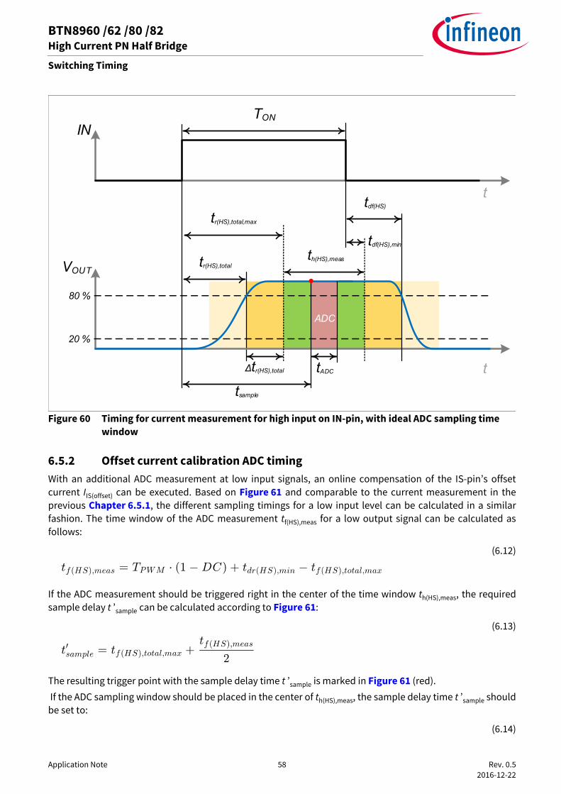
Application Note 58 Rev. 0.5 2016-12-22
BTN8960 /62 /80 /82High Current PN Half Bridge
Switching Timing
Figure 60 Timing for current measurement for high input on IN-pin, with ideal ADC sampling time window
6.5.2 Offset current calibration ADC timingWith an additional ADC measurement at low input signals, an online compensation of the IS-pin’s offsetcurrent IIS(offset) can be executed. Based on Figure 61 and comparable to the current measurement in theprevious Chapter 6.5.1, the different sampling timings for a low input level can be calculated in a similarfashion. The time window of the ADC measurement tf(HS),meas for a low output signal can be calculated asfollows:
(6.12)
If the ADC measurement should be triggered right in the center of the time window th(HS),meas, the requiredsample delay t ’sample can be calculated according to Figure 61:
(6.13)
The resulting trigger point with the sample delay time t ’sample is marked in Figure 61 (red). If the ADC sampling window should be placed in the center of th(HS),meas, the sample delay time t ’sample shouldbe set to:
(6.14)
t
IN
VOUT
t
80 %
20 %
tr(HS),total
tdf(HS)
∆tr(HS),total
th(HS),meas
tr(HS),total,max
tdf(HS),min
TON
tsample
tADC
ADC

Application Note 59 Rev. 0.5 2016-12-22
BTN8960 /62 /80 /82High Current PN Half Bridge
Switching Timing
In the case of a fault condition, the IS-pin will provide a constant current of IIS(lim), instead of the current sensefunctionality. This current IIS(lim) can be clearly distinguished from the lower offset current IIS(offset). Furtherdetails are described in Chapter 5.5.1.1.
Figure 61 Timing for current measurement for low input on IN-pin
6.6 Allowed PWM setup for current sense ADC measurementsBased on the previous Chapter 6.5, a relationship between the lowest possible duty cycle DCmin,corresponding to the minimal time TON,min, and the PWM frequency can be set up. The worst case (max.) ADCconversion time window is tADC,max. For a worst case analysis, the following assumption must be respected inany case, as the time window for the ADC measurement th(HS),meas, according to Equation (6.9), has to begreater than tADC,max:
(6.15)
For certain typical values for resistor RSR (1 kΩ 5 kΩ 10 kΩ) and certain maximal ADC conversion times tADC,max,the minimal duty cycles should be respected, as shown in Figure 62 (BTN8962TA) / Figure 65 (BTN8982TA) forRSR = 1 kΩ, Figure 63 (BTN8962TA) / Figure 66 (BTN8982TA) for RSR = 5 kΩ and Figure 64 (BTN8962TA) /Figure 67 (BTN8982TA) for RSR = 10 kΩ.
t
IN
VOUT
t
80 %
20 %
tdr(HS)tf(HS),total
∆tf(HS),total
tl(HS),meas
tf(HS),total,max tdr(HS),min
TOFF
t'sample

Application Note 60 Rev. 0.5 2016-12-22
BTN8960 /62 /80 /82High Current PN Half Bridge
Switching Timing
6.6.1 BTN8962TA
Figure 62 Minimal allowed duty cycle DCmin for a given PWM frequency fPWM, a ADC conversion time tADC and RSR = 1 kΩ, for BTN8962TA
Figure 63 Minimal allowed duty cycle DCmin for a given PWM frequency fPWM, a ADC conversion time tADC and RSR = 5 kΩ, for BTN8962TA
0 2 4 6 8 10 12 14 16 18 200
5
10
15
20
25
30
35
40
45
50
fPWM
(kHz)
min
. dut
y cy
cle
(%)
tADC max
= 0.5 µs
tADC max
= 1.0 µs
tADC max
= 2.0 µs
tADC max
= 5.0 µs
tADC max
= 10 µs
0 2 4 6 8 10 12 14 16 18 200
5
10
15
20
25
30
35
40
45
50
fPWM
(kHz)
min
. dut
y cy
cle
(%)
tADC max
= 0.5 µs
tADC max
= 1.0 µs
tADC max
= 2.0 µs
tADC max
= 5.0 µs
tADC max
= 10 µs

Application Note 61 Rev. 0.5 2016-12-22
BTN8960 /62 /80 /82High Current PN Half Bridge
Switching Timing
Figure 64 Minimal allowed duty cycle DCmin for a given PWM frequency fPWM, a ADC conversion time tADC and RSR = 10 kΩ, for BTN8962TA
6.6.2 BTN8982TA
Figure 65 Minimal allowed duty cycle DCmin for a given PWM frequency fPWM, a ADC conversion time tADC and RSR = 1 kΩ, for BTN8982TA
0 2 4 6 8 10 12 14 16 18 200
5
10
15
20
25
30
35
40
45
50
fPWM
(kHz)
min
. dut
y cy
cle
(%)
tADC max
= 0.5 µs
tADC max
= 1.0 µs
tADC max
= 2.0 µs
tADC max
= 5.0 µs
tADC max
= 10 µs
0 2 4 6 8 10 12 14 16 18 200
5
10
15
20
25
30
35
40
45
50
55
fPWM
(kHz)
min
. dut
y cy
cle
(%)
tADC max
= 0.5 µs
tADC max
= 1.0 µs
tADC max
= 2.0 µs
tADC max
= 5.0 µs
tADC max
= 10 µs

Application Note 62 Rev. 0.5 2016-12-22
BTN8960 /62 /80 /82High Current PN Half Bridge
Switching Timing
Figure 66 Minimal allowed duty cycle DCmin for a given PWM frequency fPWM, a ADC conversion time tADC and RSR = 5 kΩ, for BTN8982TA
Figure 67 Minimal allowed duty cycle DCmin for a given PWM frequency fPWM, a ADC conversion time tADC and RSR = 10 kΩ, for BTN8982TA
6.6.3 Example calculationFor an example application with the BTN8962TA, the following parameter values are assumed:• PWM frequency fPWM= 20 kHz, resulting in TPWM= 1 / fPWM = 50µs• DCmin= 25%• RSR = 1 kΩ resulting in tdf(HS),min = 1,971 µs and tr(HS),total,max = 4,321 µs
0 2 4 6 8 10 12 14 16 18 200
5
10
15
20
25
30
35
40
45
50
55
fPWM
(kHz)
min
. dut
y cy
cle
(%)
tADC max
= 0.5 µs
tADC max
= 1.0 µs
tADC max
= 2.0 µs
tADC max
= 5.0 µs
tADC max
= 10 µs
0 2 4 6 8 10 12 14 16 18 200
5
10
15
20
25
30
35
40
45
50
55
fPWM
(kHz)
min
. dut
y cy
cle
(%)
tADC max
= 0.5 µs
tADC max
= 1.0 µs
tADC max
= 2.0 µs
tADC max
= 5.0 µs
tADC max
= 10 µs

Application Note 63 Rev. 0.5 2016-12-22
BTN8960 /62 /80 /82High Current PN Half Bridge
Switching Timing
This setup results in the max. ADC conversion time window tADC,max:
(6.16)
(6.17)

Application Note 64 Rev. 0.5 2016-12-22
BTN8960 /62 /80 /82High Current PN Half Bridge
Power Dissipation
7 Power DissipationThe device dissipates some power. This power dissipation is generated in the top chip and in the individualMOSFETs. The high currents in the MOSFETs generate most of the power dissipation. The followingconsideration is based on several assumptions, so the result is ultimately an estimation which should help youunderstand the general trend. The power dissipation in the MOSFETs consists mainly of conducted losses and switching losses. Losses in thebody diode only occur during the cross current protection phase. They are therefore not taken intoconsideration.
7.1 Power dissipation of the control chip (top chip)The control chip consumes a certain amount of current, and this causes power dissipation. In DC-mode the following equation describes the power dissipation in the control chip:
(7.1)
In PWM-mode, an additional current is needed to charge/discharge the MOSFET gates. This leads to thefollowing PWM power dissipation:
(7.2)
The gate charges for the BTN89xx are specified in the table below:
Power dissipation in the control chip can be calculated as follows:
(7.3)
7.2 Conduction power dissipationIn the ON-state, a MOSFET has a specific RON which is listed in the data sheet. RON is different for the high-side(HS) and the low-side (LS) MOSFETs. This means that RON must be selected according to the driving situation.A current flowing through this transistor generates the following conducted losses:
(7.4)
In case the NovalithIC™ is driven in a static condition, Equation (7.4) can be used to estimate the staticconducted losses for the high-side or low-side MOSFET.
Table 3 Qtot of BTN896x and BTN898xProduct Total gate chargeBTN8960 /62 450 nC
BTN8980 /82 550 nC
SISONVsDCCC VIIP ⋅+=− )( )(
PWMStotPWMCC fVQP ⋅⋅=−
PWMStotSISONVsPWMCCDCCCCC fVQVIIPPP ⋅⋅+⋅+=+= −− )( )(
ONCL RIP ⋅= 2

Application Note 65 Rev. 0.5 2016-12-22
BTN8960 /62 /80 /82High Current PN Half Bridge
Power Dissipation
7.3 Power dissipation due to switchingWith PWM control, switching losses need to be taken into account because they generate most of the powerdissipation for high PWM frequencies. The NovalithICTM devices are designed to drive motors or otherinductive loads. This chapter deals with switching losses that are generated while driving an inductive load.
Figure 68 High-side switching scenario of BTN89xy
The current in an inductor cannot be changed abruptly (rule of Lenz). As shown in Figure 68, the current in thehigh-side (HS) MOSFET is driven by the motor inductance as long as the OUT voltage drops one VBE below GNDand the current is flowing through the body diode of the low-side (LS) MOSFET. This means that the current IHSis flowing in the high-side (HS) MOSFET, even though this is in linear mode during tHS-off. The NovalithICTM has a cross-current protection mechanism which ensures that an output MOSFET is turnedon only when the other one is off. This causes a free wheeling current through the MOSFET body diode (VBE inFigure 68) before the resistive path is switched on. The power dissipation caused by the body diode isnegligible and thus not taken into account in this estimation. The rise- and fall- time in the data sheet is the period during which the output voltage decreases from 80% to20%. In order to determine the switching losses, we need to determine the time required to decrease theoutput voltage from 100% to 0%. The tHS-off can be estimated from the data sheet parameters with theEquation (7.5) accordingly.
(7.5)
For the other switching times (tHS-on, tLS-off and tLS-on) Equation (7.5) can be used to perform the samecalculation using the corresponding data sheet parameters (tr(HS), tf(LS) and tr(LS)).Other assumptions, with a minor effect on the result, include the following: • The load current during the switching process is constant. • VOUT and VDS(HS) have linear behavior. • The switching times are assumed as equal and in the following always referred to as tHS-off.
M
Vs
OUT
GND
VDS(HS)
D
S
D
S
HS
LS
t
IHS
ILS
VOUT
t
IOUT
VDS(HS)
VOUT
IHS
ILS
ESL
ESL
VRon,act
VBE
ON OFF
OFF
tHS-off
tHS-off
tSL1 tSL2
VRon,FW
Factor 0.5 is related to ∆VOUT from 0% to 100%5.0
)( HSfoffHS
tt =−

Application Note 66 Rev. 0.5 2016-12-22
BTN8960 /62 /80 /82High Current PN Half Bridge
Power Dissipation
The switching energy ESL is shown in Figure 68 and can be estimated using Equation (7.6) below:
(7.6)
From the switching energy ESL the average power loss PSL can be determined with two switching times perPWM period. This is shown in Equation (7.7):
(7.7)
7.4 Entire power dissipation of the MOSFETsThe average power dissipation in PWM-mode consists of the switching losses plus the conducted losses, asshown in Figure 69. We must take into account that the losses occur in the high-side (HS) and low-side (LS)MOSFET. In the example of Figure 68, where the motor is connected to GND, the switching losses occur in thehigh-side (HS) MOSFET. The conducted losses occur in the high-side (HS) MOSFET during the ON-phase and inthe low-side (LS) MOSFET in the free wheeling phase, as shown in Figure 69.In PWM-mode, the PWM-period-time is:
(7.8)
The duty cycle (DC) of the PWM-mode is the relation between the ON-time and the PWM-period-time inpercent.
(7.9)
offHSOUTS
t
tOUTSSL tIVdtIVE
SL
SL
−⋅⋅
=⋅⋅= ∫ 2
2
1
PWMoffHSOUTSPWMoffHSOUTS
SL ftIVftIVP ⋅⋅⋅=⋅⋅⋅⋅
= −−22
PWMPWM f
T 1=
PWM
ON
TTDC =

Application Note 67 Rev. 0.5 2016-12-22
BTN8960 /62 /80 /82High Current PN Half Bridge
Power Dissipation
Figure 69 Entire power dissipation of BTN89xy with the motor connected to GND
In Chapter 7.4.2 and Chapter 7.4.3 the power dissipation is estimated separately for the high-side (HS) andlow-side (LS) MOSFET.
7.4.1 PWM control and the duty cycle constraintsIf tFW is close to or below zero, no freewheeling occurs. VOUT does not go below GND. This means that onlyswitching losses are generated. Thus, a duty cycle generating tFW ≤ 0 is insufficient to control the motor currentand therefore not taken into account in the following calculations. In this case, the high-side (HS) MOSFETshould be permanently on.The same is valid for tON ≤ 0. In this case, the low-side (LS) MOSFET should be permanently on.Extremely low or high duty cycle values required by real applications can be achieved by increasing theswitching speed and/or by increasing TPWM.
7.4.2 Entire power dissipation in the actuator MOSFETIn the motor-to-GND scenario the actuator MOSFET is the high-side (HS) MOSFET, as in Figure 68 and inmotor-to-Vs scenario, the actuator MOSFET is the low-side (LS) MOSFET. The entire power dissipation consistsof two times the switching losses plus the conducted losses in the ON-phase, as shown in Figure 69. The timeof the ON-phase in PWM-mode is provided by the following formulae:
(7.10)
As mentioned in “Other assumptions,” on Page 65 switching times are assumed as equal and named as tHS-
off:
(7.11)
Equation for estimate the total conducted energy in the actuator MOSFET:
(7.12)
t
t
VOUT
VIN TON = TPWM · DC
actuator losses
conducted losses
(free wheeling )
conducted losses
(ON-phase )switc
hing
lo
sses
switc
hing
lo
sses
TPWM
onHSONON tTt −−=
offHSONON tTt −−=
ONactONOUToffHSOUTSONSLact tRItIVEEE ⋅⋅+⋅⋅=+⋅= − ,22

Application Note 68 Rev. 0.5 2016-12-22
BTN8960 /62 /80 /82High Current PN Half Bridge
Power Dissipation
From Equation (7.12) the average power dissipation in the actuator MOSFET can be determined bymultiplying Equation (7.12) by fPWM:
(7.13)
Equation (7.13) is an estimation of the average power dissipation in the actuator MOSFET. In Figure 68, thisis the high-side (HS) MOSFET.
7.4.3 Entire power dissipation in the freewheeling MOSFETIn the motor-to-GND scenario, the freewheeling MOSFET is the low-side (LS) MOSFET, as in Figure 68, and inthe motor-to-Vs scenario, the freewheeling MOSFET is the high-side (HS) MOSFET. The entire powerdissipation consists of the conducted losses in the freewheeling phase, as shown in Figure 69. The durationof the freewheeling phase in PWM-mode is provided by the equation below:
(7.14)
Important note: For the proper use of Equation (7.14) refer to Chapter 7.4.1.
Equation to determine the entire freewheeling energy in the freewheeling MOSFET:
(7.15)
From Equation (7.15) the average power dissipation in the freewheeling MOSFET can be determined bymultiplying Equation (7.15) by fPWM:
(7.16)
Equation (7.16) is an estimation of the average power dissipation in the freewheeling MOSFET. In Figure 68,this is the low-side (LS) MOSFET.
7.5 Entire power dissipation in the NovalithICTM
To determine the entire power dissipation in the NovalithICTM, combine Equation (7.13), Equation (7.16) andEquation (7.3).
(7.17)
Equation (7.17) is the average of the different power losses in one PWM period, as shown in Figure 69, plusthe power losses in the control chip.
7.6 SimplificationsBecause the losses in the control chip are typically negligible in comparison with the losses in the MOSFETs,they are neglected in this simplification.
PWMONactONOUToffHSOUTSPWMactact ftRItIVfEP ⋅⋅⋅+⋅⋅=⋅= − )( ,2
offHSONPWMFW tTTt −−−=
)(,2
,2
offHSONPWMFWONOUTFWFWONOUTFW tTTRItRIE −−−⋅⋅=⋅⋅=
PWMoffHSONPWMFWONOUTPWMFWFW ftTTRIfEP ⋅−−⋅⋅=⋅= − )(,2
CCFWactNova PPPP ++=

Application Note 69 Rev. 0.5 2016-12-22
BTN8960 /62 /80 /82High Current PN Half Bridge
Power Dissipation
Taking into account that the high-side (HS) and the low-side (LS) MOSFET are in a similar RON range, theequation for determining the entire power dissipation in the NovalithICTM can be significantly reduced byusing the same RON for both the high-side (HS) and the low-side (LS) MOSFET. The more conservative approachis to use the higher RON of both. The idea behind this is to have the same RON for the conducted losses of the ON- and the freewheeling phase,according to Figure 69. Due to this simplification the energy in one PWM- period is two times the switchinglosses ESL and RON losses during the remaining time:
(7.18)
(7.19)
From the simplified NovalithICTM energy to the simplified NovalithICTM power dissipation by multiplyingEquation (7.19) by fPWM:
(7.20)
)2(2 offHSPWMCLSLNova tTPEE −⋅−⋅+⋅=
)2(2
2 2offHSPWMONOUToffHS
OUTSNova tTRItIVE −− ⋅−⋅⋅+⋅
⋅⋅=
PWMoffHSPWMONOUToffHSOUTSSNova ftTRItIVP ⋅⋅−⋅⋅+⋅⋅= −− ))2(( 2,

Application Note 70 Rev. 0.5 2016-12-22
BTN8960 /62 /80 /82High Current PN Half Bridge
Thermal Performance
8 Thermal PerformanceThe PCB used for the simulation is compliant with JEDEC 2s2p (JESD 51-5, JESD 51-7) and JEDEC 1s0p (JESD51-3), as described in Table 4. For 1s0p, a cooling area of 600 mm² and 300 mm² is additionally considered.
The cross section of JEDEC 2s2p is shown in Figure 70.
Figure 70 Cross section JEDEC 2s2p
The cross section of JEDEC 1s0p is shown in Figure 71.
Figure 71 Cross section JEDEC 1s0p
Table 4 PCB specificationDimensions 76.2 × 114.3 × 1.5 mm³ λtherm [W/m • K]
Material FR4 0.3
Metallization JEDEC 2s2p (JESD 51-7) + (JESD 51-5)JEDEC 1s0p (JESD 51-3) + Cooling Area
388
Cooling Area 600 mm², 300 mm², footprint
Thermal Vias Ø = 0.3 mm; plating 25 µm; 40 pcs.
Package Attach [50 µm] Solder 55
4 layer PCB35µm / 100%*
35µm / 100%*70µm / 5%*
70µm‚ modeled (traces)
*: means percentual Cu metalization on each layer
1,5
mm
*: means percentual Cu metalization on each layer
4 layer PCB
70µm / 5%*
70µm‚ modeled (traces, cooling area)
1,5
mm

Application Note 71 Rev. 0.5 2016-12-22
BTN8960 /62 /80 /82High Current PN Half Bridge
Thermal Performance
8.1 Zth simulation results
Figure 72 Zth-ja for BTN8960/62, in PG-TO263-7-1, (LSS: low-side switch, HSS: high-side switch)
Figure 73 Zth-ja for BTN8980/82, in PG-TO263-7-1, (LSS: low-side switch, HSS: high-side switch)
0
10
20
30
40
50
60
70
80
0.00001 0.001 0.1 10 1000
Zth-
ja [K
/W]
time [sec]
LSS - 1s0p / 600mm²HSS - 1s0p / 600mm²LSS - 1s0p / 300mm²HSS - 1s0p / 300mm²LSS - 1s0p / footprintHSS - 1s0p / footprintLSS - 2s2pHSS - 2s2p
0
10
20
30
40
50
60
70
80
0.00001 0.001 0.1 10 1000
Zth-
ja [K
/W]
time [sec]
LSS - 1s0p / 600mm²HSS - 1s0p / 600mm²LSS - 1s0p / 300mm²HSS - 1s0p / 300mm²LSS - 1s0p / footprintHSS - 1s0p / footprintLSS - 2s2pHSS - 2s2p
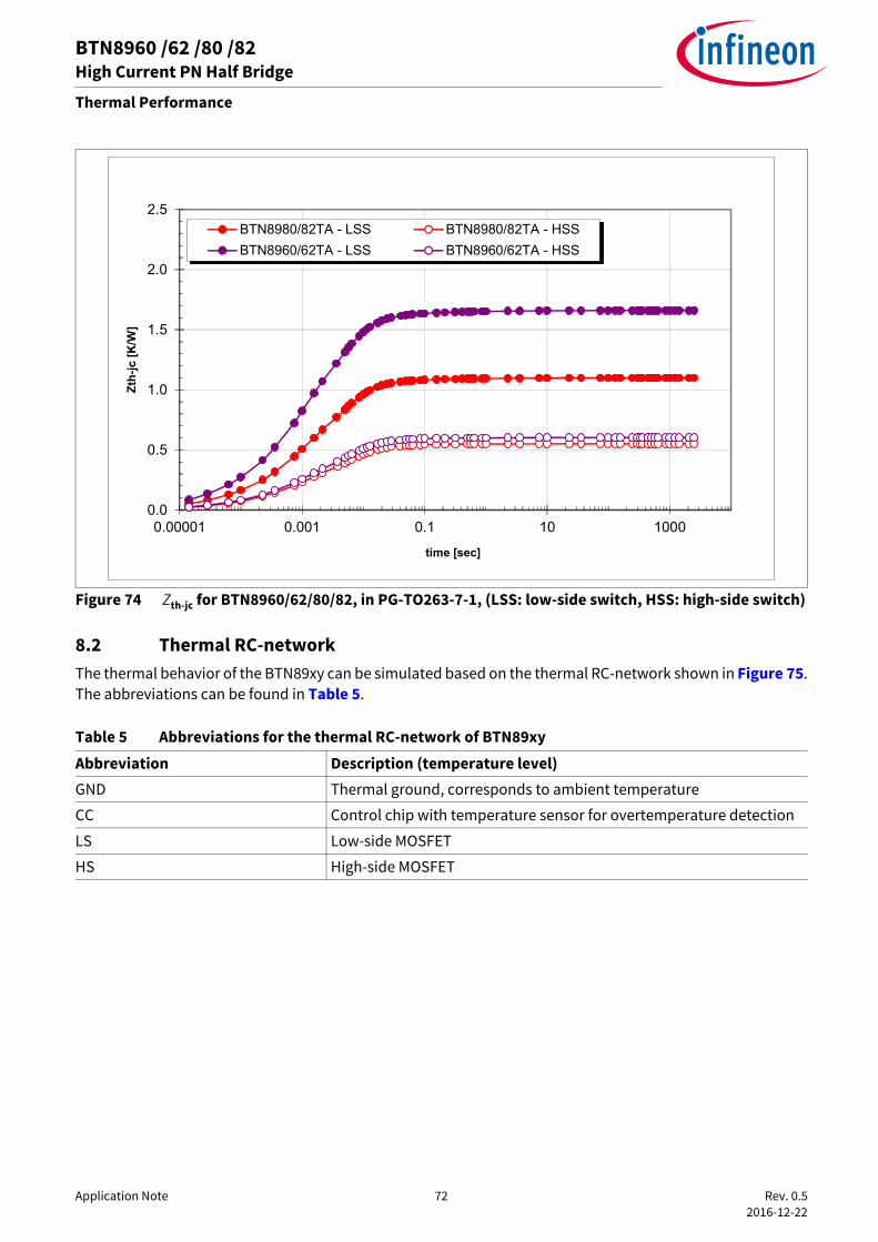
Application Note 72 Rev. 0.5 2016-12-22
BTN8960 /62 /80 /82High Current PN Half Bridge
Thermal Performance
Figure 74 Zth-jc for BTN8960/62/80/82, in PG-TO263-7-1, (LSS: low-side switch, HSS: high-side switch)
8.2 Thermal RC-networkThe thermal behavior of the BTN89xy can be simulated based on the thermal RC-network shown in Figure 75.The abbreviations can be found in Table 5.
Table 5 Abbreviations for the thermal RC-network of BTN89xyAbbreviation Description (temperature level)GND Thermal ground, corresponds to ambient temperature
CC Control chip with temperature sensor for overtemperature detection
LS Low-side MOSFET
HS High-side MOSFET
0.0
0.5
1.0
1.5
2.0
2.5
0.00001 0.001 0.1 10 1000
Zth-
jc [K
/W]
time [sec]
BTN8980/82TA - LSS BTN8980/82TA - HSSBTN8960/62TA - LSS BTN8960/62TA - HSS

Application Note 73 Rev. 0.5 2016-12-22
BTN8960 /62 /80 /82High Current PN Half Bridge
Thermal Performance
Figure 75 Schematic of the thermal RC-network for BTN89xy
R9
C4
R1C1
R2 C2
R3C3
R6 C6
R7C7
R8 C8R19
R12
R4
R25
R26
R20C18
R21 C19
R22C20
R23
C23
C24
C11
C17
R13
C12
R10C10
C13
R15C14
R16C15
R17C16
R14
R11
R18
C5
R5
HSLS
CC

Application Note 74 Rev. 0.5 2016-12-22
BTN8960 /62 /80 /82High Current PN Half Bridge
Thermal Performance
8.2.1 Parameters for BTN8960/62For the thermal RC-network, which is shown in Figure 75, the values of the BTN8960/62 for the resistors canbe found in Table 6 and for the capacities in Table 7, depending on the test condition (PCB).
Table 6 Thermal RC-network resistor values for BTN8960/62Parameter 1s0p 2s2p 300 mm² 600 mm²R1 4.13479 6.14635 4.36197 3.28848
R2 9.49529 6.99412 8.86409 10.2156
R3 6.04676 6.24923 6.00779 5.73654
R4 1997.68 1999.98 9989.45 9989.4
R5 24.6962 14.3669 26.5405 23.2126
R6 0.765526 0.825716 0.784931 0.793983
R7 709.461 21.7132 712.375 703.027
R8 24.0397 959.748 98.4013 83.6365
R9 0.509237 0.277148 0.267684 0.257237
R10 0.0201271 0.219217 0.159445 0.17652
R11 0.0134086 0.753008 0.0120334 0.0123115
R12 48.4465 75.4798 187.262 157.461
R13 2.15834 0.703103 41.9972 47.1135
R14 827.333 312.256 793.297 744.845
R15 1.89889 1.16198 1.93861 1.90089
R16 5.67666 1.27492 3.89945 3.75373
R17 30.7871 257.22 3.29846 4.09169
R18 954.388 1715.55 685.267 466.671
R19 0.666271 183.372 1.66419 2.4898
R20 9.17544 11.5243 49.7984 49.454
R21 8.86655 132.758 4.50777 5.96947
R22 3.64248 4.55264 20.7864 22.0143
R23 1.54282 47.1593 9.53249 12.2849
R25 0.0115874 0.0111131 0.0120082 0.0107333
R26 59.2163 3.41491 16.2884 10.0589

Application Note 75 Rev. 0.5 2016-12-22
BTN8960 /62 /80 /82High Current PN Half Bridge
Thermal Performance
8.2.2 Parameters for BTN8980/82For the thermal RC-network, which is shown in Figure 75, the values of the BTN8980/82 for the resistors canbe found in Table 8 and for the capacities in Table 9, depending on the test condition (PCB).
Table 7 Thermal RC-network capacitor values for BTN8960/62Parameter 1s0p 2s2p 300 mm² 600 mm²C1 9.01E-07 8.11E-06 9.00E-06 1.33E-05
C2 0.0096747 0.00768932 0.00857854 0.0093771
C3 0.00328475 0.00461763 0.00376799 0.00326148
C4 0.00117103 0.0011541 0.0011511 0.00116079
C5 1.92349 0.419775 2.01168 2.98621
C6 0.259815 0.361034 0.236595 0.25227
C7 2.30445 1.17886 0.502516 0.85818
C8 0.0924509 0.169357 0.147342 0.233769
C10 0.0759261 0.000081424 0.146105 0.138098
C11 0.874947 0.681589 0.005741 0.00594316
C12 0.0219339 0.641786 0.40078 0.441664
C13 0.00211971 0.00072605 0.00200476 0.00193489
C14 0.0518487 0.0149359 0.0742448 0.0420656
C15 0.45993 0.0446105 0.746801 0.67808
C16 0.264822 0.17218 0.253172 0.228248
C17 2.00613 0.960968 0.182447 0.152115
C18 0.0477427 0.157112 0.3562 0.3517
C19 2.21387 7.70672 1.95155 1.56875
C20 5.75675 17.92 2.706 1.05419
C23 0.482909 0.455128 0.00175319 0.00109187
C24 0.00483449 0.00210439 0.0014892 0.00143505
Table 8 Thermal RC-network resistor values for BTN8980/82Parameter 1s0p 2s2p 300 mm² 600 mm²R1 14.7357 14.607 14.5115 14.4932
R2 1.41757 2.99853 0.892556 0.662104
R3 4.68444 2.59111 4.77943 5.04297
R4 417.267 996.831 999.052 962.665
R5 112.975 18.9927 52.4443 41.5135
R6 0.631354 0.586299 0.663352 0.592812
R7 32.786 17.7176 12.9216 10.8754
R8 238.436 60.6471 141.19 133.593
R9 0.010794 0.253683 0.0664578 0.0534714

Application Note 76 Rev. 0.5 2016-12-22
BTN8960 /62 /80 /82High Current PN Half Bridge
Thermal Performance
R10 0.697554 0.0136973 0.843804 0.729177
R11 0.457247 0.800679 0.0121925 0.527079
R12 3.16907 0.309781 0.0990132 0.729318
R13 0.863968 608.83 4.30397 0.308658
R14 122.484 743.102 993.339 108.893
R15 0.922458 0.943908 1.03571 0.725828
R16 63.0068 28.9428 23.0979 13.6581
R17 16.2261 14.9297 20.1678 13.6112
R18 14.9109 0.01 18.7873 15.8732
R19 269.376 711.221 999.114 998.955
R20 31.986 15.9504 33.3671 24.8793
R21 14.5539 11.788 2.37429 2.66703
R22 19.4019 24.147 18.495 13.1898
R23 15.6402 1.70354 20.424 20.3062
R25 0.0102647 0.0180739 0.0147595 0.0992122
R26 5.9597 2.67745 2.46301 2.16571
Table 8 Thermal RC-network resistor values for BTN8980/82Parameter 1s0p 2s2p 300 mm² 600 mm²

Application Note 77 Rev. 0.5 2016-12-22
BTN8960 /62 /80 /82High Current PN Half Bridge
Thermal Performance
Table 9 Thermal RC-network capacitor values for BTN8980/82Parameter 1s0p 2s2p 300 mm² 600 mm²C1 0.0109887 0.0122742 0.0117668 0.0114942
C2 4.38961E-06 1.75918E-06 1.13147E-05 0.00010077
C3 0.00361686 0.00382319 0.00452151 0.00335106
C4 0.00117385 0.00118004 0.0011766 0.00117587
C5 0.0144137 0.400558 0.186452 0.249974
C6 0.064702 0.0424699 0.0426304 0.0280119
C7 0.124171 0.0566395 0.407592 0.66619
C8 0.0184178 0.840657 0.061641 0.224521
C10 0.127647 0.0215798 0.0135012 0.130117
C11 0.219454 0.965128 0.201947 0.289226
C12 0.0757321 0.0222976 0.280791 0.460985
C13 0.0020413 0.00210601 0.00223527 0.0013234
C14 0.0489809 0.0743878 0.105303 0.018626
C15 0.28671 0.102 0.411468 0.464271
C16 0.00598831 0.0157598 0.00766389 0.00254175
C17 0.000668051 0.171968 0.0555266 0.0541936
C18 0.801461 3.05061 1.75168 0.000842353
C19 0.00214924 4.84858 0.365562 0.0312806
C20 5.63547 6.30449 2.98494 7.0397
C23 0.348292 0.184817 0.3862 0.261893
C24 0.0995441 0.242926 0.180138 0.116301

Application Note 78 Rev. 0.5 2016-12-22
BTN8960 /62 /80 /82High Current PN Half Bridge
Revision History
9 Revision History
Revision Date Changes0.5 2016-12-22 Chapter 1 updated.
Chapter 4.3 added.Chapter 5.5.2.3 added.Chapter 6: updatedStyle Guide update.Editorial changes.
0.4 2015-07-02 Page 18, Figure 11: Motor shunt replaced.Page 67, Figure 69: TON and DC new description.Chapter 5.5 added.Chapter 6 added.Chapter 8 added.Style Guide update.Editorial changes.
0.3 2014-08-29 Page 17 - Chapter 4.4: Added.Page 18 - Chapter 7.2: Text update.Page 64 - Chapter 7: Added.Chapter 2: Updated application circuits (C1 and DC-link)
0.2 2013-01-16 Page 5 - Chapter 2: Added benefits.Page 5 - Figure 2; Page 6 - Figure 3; Page 11 - Other Components: Changed resistor name from R1 to R3 and CIS-value to 1nF and CIS-text.Page 12: Updated Figure 7.Page 5 - Figure 2, Page 6 - Figure 3: Update value of C1.Page 10 - Figure 6: Update footnote of figure.Page 20: New Chapter 5.
0.1 2012-07-09 Initial release.

Trademarks of Infineon Technologies AGµHVIC™, µIPM™, µPFC™, AU-ConvertIR™, AURIX™, C166™, CanPAK™, CIPOS™, CIPURSE™, CoolDP™, CoolGaN™, COOLiR™, CoolMOS™, CoolSET™, CoolSiC™,DAVE™, DI-POL™, DirectFET™, DrBlade™, EasyPIM™, EconoBRIDGE™, EconoDUAL™, EconoPACK™, EconoPIM™, EiceDRIVER™, eupec™, FCOS™, GaNpowIR™,HEXFET™, HITFET™, HybridPACK™, iMOTION™, IRAM™, ISOFACE™, IsoPACK™, LEDrivIR™, LITIX™, MIPAQ™, ModSTACK™, my-d™, NovalithIC™, OPTIGA™,OptiMOS™, ORIGA™, PowIRaudio™, PowIRStage™, PrimePACK™, PrimeSTACK™, PROFET™, PRO-SIL™, RASIC™, REAL3™, SmartLEWIS™, SOLID FLASH™,SPOC™, StrongIRFET™, SupIRBuck™, TEMPFET™, TRENCHSTOP™, TriCore™, UHVIC™, XHP™, XMC™.
Trademarks updated November 2015
Other TrademarksAll referenced product or service names and trademarks are the property of their respective owners.
Edition 2016-12-22Published by Infineon Technologies AG81726 Munich, Germany
© 2016 Infineon Technologies AG.All Rights Reserved.
Do you have a question about any aspect of this document?Email: [email protected]
Document reference<Doc_Number>
IMPORTANT NOTICEThe information contained in this application note isgiven as a hint for the implementation of the productonly and shall in no event be regarded as a descriptionor warranty of a certain functionality, condition orquality of the product. Before implementation of theproduct, the recipient of this application note mustverify any function and other technical informationgiven herein in the real application. InfineonTechnologies hereby disclaims any and all warrantiesand liabilities of any kind (including without limitationwarranties of non-infringement of intellectualproperty rights of any third party) with respect to anyand all information given in this application note.
The data contained in this document is exclusivelyintended for technically trained staff. It is theresponsibility of customer’s technical departments toevaluate the suitability of the product for the intendedapplication and the completeness of the productinformation given in this document with respect tosuch application.
For further information on technology, delivery termsand conditions and prices, please contact the nearestInfineon Technologies Office (www.infineon.com).
WARNINGSDue to technical requirements products may containdangerous substances. For information on the typesin question please contact your nearest InfineonTechnologies office.
Except as otherwise explicitly approved by InfineonTechnologies in a written document signed byauthorized representatives of Infineon Technologies,Infineon Technologies’ products may not be used inany applications where a failure of the product or anyconsequences of the use thereof can reasonably beexpected to result in personal injury.
Please read the Important Notice and Warnings at the end of this document