Embed Size (px)
Citation preview
1
Electronic and optical properties of boron-doped nanocrystalline diamond films
W. Gajewski1, P. Achatz2,3, O.A. Williams4, K. Haenen4, E. Bustarret2,
M. Stutzmann1 and J.A. Garrido1
1 Walter Schottky Institut, TU München, Am Coulombwall 3, 85748 Garching, Germany
2 Institut Néel, CNRS & Université Joseph Fourier, BP-166, 38042 Grenoble, France
3 CEA, INAC, SPSMS, LaTEQS, F-38054 Grenoble Cedex 9, France
4 Institute for Materials Research (IMO), Hasselt University and Division IMOMEC, IMEC vzw, Wetenschapspark 1, 3590,
Belgium
We report on the electronic and optical properties of boron-doped nanocrystalline diamond
(NCD) thin films grown on quartz substrates by CH4/H2 plasma chemical vapor deposition.
Diamond thin films with a thickness below 350 nm and with boron concentration ranging from
1017cm-3 to 1021 cm-3 have been investigated. UV Raman spectroscopy and AFM have been used
to assess the quality and morphology of the diamond films. Hall effect measurements confirmed
the expected p-type conductivity. At room temperature, the conductivity varies from 1.5x10⁻⁸ Ω-
1cm-1 for a non-intentionally doped film up to 76 Ω-1cm-1 for a heavily B-doped film. Increasing
the doping level results in a higher carrier concentration while the mobility decreases from 1.8
cm2V-1s-1 down to 0.2 cm2V-1s-1. For NCD films with low boron concentration, the conductivity
strongly depends on temperature. However, the conductivity and the carrier concentration are no
longer temperature-dependent for films with the highest boron doping, and the NCD films
exhibit metallic properties. Highly doped films show superconducting properties with critical
temperatures up to 2K. The critical boron concentration for the metal-insulator transition is in the
range from 2x1020 cm-3 up to 3x1020 cm-3. We discuss different transport mechanisms to explain
the influence of the grain boundaries and boron doping on the electronic properties of NCD
films. Valence band transport dominates at low boron concentration and high temperatures,
2
whereas hopping between boron acceptors is the dominant transport mechanism for boron
doping concentration close to the Mott transition. Grain boundaries strongly reduce the mobility
for low and very high doping levels. However, at intermediate doping levels where hopping
transport is important, grain boundaries have a less pronounced effect on the mobility. The
influence of boron and the effect of grain boundaries on the optoelectronic properties of the NCD
films are examined using spectrally resolved photocurrent measurements and photothermal
deflection spectroscopy. Major differences occur in the low energy range, between 0.5 – 1.0 eV,
where both Boron impurities and the sp2 carbon phase in the grain boundaries govern the optical
absorption.
I. INTRODUCTION
Nanocrystalline diamond (NCD) thin films have, among other outstanding properties, a remarkable
hardness, low friction coefficient, optical transparency in the ultraviolet, visible, and infrared, as well
as a low electron emission threshold voltage. Different applications have been so far reported in which
NCD films were used for high-frequency surface acoustic wave devices,1,2 Micro-Electro-Mechanical
Systems (MEMS),3 MESFETs,4 and enduring coating.5,6 Due to its biocompability and chemical
stability, NCD films have also attracted attention for bioelectrochemical applications.7,8,9 In addition,
considerable efforts have been dedicated to optimize the growth process: its dependence on gas
preparation and precursor molecules,10,11 as well as the influence of the substrate material.12,13 The
growth and structural properties of NCD films and ultrananocrystalline diamond (UNCD) films have
been recently compared.14 So far, the n-type conductivity induced by nitrogen addition during UNCD
growth has been investigated in detail.15,16 The p-type doping of diamond with boron has been
extensively examined in single crystal (SCD) homoepitaxially grown material,17,18,19,20 as well as in
3
polycrystalline materials (PCD).21,22 In the case of heavily boron doped samples, superconductivity has
been reported.23,24 Finally, the influence of the boron acceptor on the structural and optoelectronic
properties of the diamond films were investigated for single and polycrystalline diamond films.21,22,26-31
However, the same sort of detailed investigation is still missing for boron-doped NCD films. As it has
been discussed for polycrystalline diamond films22 and UNCD films,32 it is essential to understand the
influence of the grain boundaries on the optical properties of NCD and the role they play in the
electronic transport. Recently, several papers have reported on the structural properties of NCD films,
as revealed by Raman spectroscopy in low33-35 and in high boron doped diamond films.35-38 The
characteristic Fano resonance behavior was observed for heavily doped NCD films.39 However, a
comprehensive study on the electronic properties has not yet been published. Some data can be found
in articles focused on the NCD structure25,37 or in a recently published work on the superconductivity of
boron-doped nanocrystalline diamond.39
In this work we have systematically investigated the structural, electronic, and optical properties of
NCD films with boron concentrations from 1016 cm-3 up to 1021 cm-3. Ultraviolet micro-Raman
spectroscopy was used to study the structural properties of the NCD films. Temperature dependent Hall
effect experiments and conductivity experiments were applied to investigate the influence of boron on
the electronic properties of NCD films. Finally, UV-Vis spectroscopy, spectrally resolved
photoconductivity and photothermal deflection spectroscopy were used to study the optical properties
and the influence of the grain boundaries.
The experiments reveal that the conductivity can be well controlled by the boron content in the gas
phase, resulting in NCD films behaviors ranging from insulating to metallic. Different electronic
transport mechanisms can be observed depending on the concentration of boron in NCD films. While
transport in the valence band is expected at high temperature in the non-intentionally doped (n.i.d.) and
weakly boron-doped films, metal-like conductivity dominates in films with boron concentration above
4
2x1020 cm-3. For intermediate boron doping (2x10¹⁹ – 3x1020 cm-3), hopping between boron acceptors
is assumed to be the dominant transport mechanism in the NCD films. At low temperatures and low
boron concentration, hopping transport in the grain boundaries is expected to become important. In
other polycrystalline materials, such as micro- and nanocrystalline Si, electronic transport is strongly
influenced by the potential barriers at the grain boundaries, as demonstrated by Seto.49 We have also
addressed this possibility in the case of NCD. However, in contrast to Si, we have found that the effect
of grain boundaries is much lower for nanocrystalline diamond due to the large activation energy of the
boron acceptor in diamond. Highly doped films show superconducting properties with critical
temperatures of about 2K. A doping-induced metal-insulator transition is observed, with critical boron
concentrations in the range from 2x1020 cm-3 up to 3x1020 cm-3. The electronic transport data are in
good agreement with the results of the photocurrent experiments. The boron incorporation results in an
increase of the film conductivity and a simultaneous photocurrent increase in the low energy range (0.5
- 1.0 eV). The photocurrent onset observed for the boron-free and n.i.d. NCD films at about 1.0 eV is
tentatively assigned to the contribution of sp2 bonded carbon in the grain boundaries.. The optical
absorption coefficient estimated from photothermal deflection spectroscopy is in good agreement with
the results of the photocurrent experiments, confirming the dominant role of the sp2 phase on the
optical properties of NCD.
II. EXPERIMENTAL SECTION
Nanocrystalline diamond films with different boron concentration were grown on quartz substrates.
The quartz substrates were seeded ultrasonically in a solution containing nano-diamond powder40 and
films were grown in a Microwave Plasma Enhanced Chemical Vapor Deposition (MWPECVD) reactor
using conventional CH4/H2 plasma with a methane concentration below 5%. The boron doping was
controlled by adding TriMethylBoron (TMB) to the gas phase, with B:C ratios up to 6600 ppm.
5
Prior to any characterization, “as-grown” films were cleaned in ultrasonic baths of acetone and
isopropanol. Raman spectroscopy was performed at ambient conditions using a Dilor XY double
monochromator spectrometer, together with an Ar+ ion laser (514,5 nm line) as well as the Dilor
labram Infinity with a 325 nm line of the HeCd laser. The surface morphology was examined with a
Veeco Nanoscope III AFM in tapping mode under ambient conditions. In order to avoid the influence
of the H-induced surface conductivity on the electronic transport experiments, the NCD films were
oxidized using oxygen plasma (5 min, 200W, 1.4 mbar). Ti/Au (20/200nm) metal contacts were
evaporated in a van der Pauw configuration to investigate the electronic properties of the NCD films.
Conductivity and Hall effect measurements were performed using an Oxford cryostat in the
temperature range from 70K to 610K. For the Hall effect characterization, an alternating magnetic field
of 1.8 T was used. The temperature dependence of the conductivity in the so-called low temperature
regime, down to 350mK, was investigated using a Quantum Design Physical Properties Measurements
System, employing a four terminal configuration for the contacts. The optical properties were
investigated using Spectrally Resolved Photoconductivity (SPC) and Photothermal Deflection
Spectroscopy (PDS). In both cases chopped (4 Hz) monochromatic light from either a halogen or xenon
arc lamp were used for the optical excitation in the energy range 0.3 – 6.2 eV. The photoresponse was
detected by a lock-in amplifier and normalized to the number of incident photons measured by a
pyroelectric detector. The photoconductivity measurements were carried out in vacuum (10-6 mbar), in
the temperature range 80 and 360 K using a liquid nitrogen cryostat. The applied bias to the samples
during the experiments was in the range 20-35 V. The PDS measurements were performed at room
temperature using perfluorhexane as the deflection medium.
Secondary ion mass spectroscopy was performed by the Centre for Surface and Materials Analysis
(CSMA Ltd.) in England, using a Cameca IMS 4f double focusing secondary ion mass spectrometer
with 12.5 kV O2+ primary beam. Under incident angle of 30° to normal with a nominal impact energy
6
of 8 kV per O2+ ion, the sputtering was about 5 Å/s. Calibration was performed using a 5x1014 cm-2 11B
ion implanted diamond-like carbon standard.
III. RESULTS AND DISCUSSION
A. Structural Properties
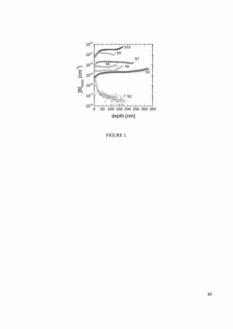
As derived from SIMS measurements, the boron concentration in the NCD films varies from 9.7x10¹⁶
cm-3 in the non-intentionally doped (n.i.d.) film up to 3.3x1021 cm-3 in the heavily boron doped NCD
film (Table I). The SIMS profiles for B-doped NCD films are depicted in Fig. 1. The presence of boron
in the n.i.d. film results from the memory effect (due to boron contamination) in the growth chamber. A
reference film (S1) was grown in a boron-free reactor. It was confirmed that the method applied for
seeding has an important impact on the quality of the NCD films14 and thus, the efficiency of doping
can be increased: see for instance the properties of samples S4, seeded mechanically and with 150 ppm
of TMB in the gas phase, and S5, seeded in ultrasonic bath with 10 ppm of TMB in the gas phase.
However, the influence of the chamber memory effect on the final effective boron doping of the NCD
films can not be excluded. Further measurements should be performed in order to clarify the
dependence of the effective boron doping on TMB concentration in the gas phase.
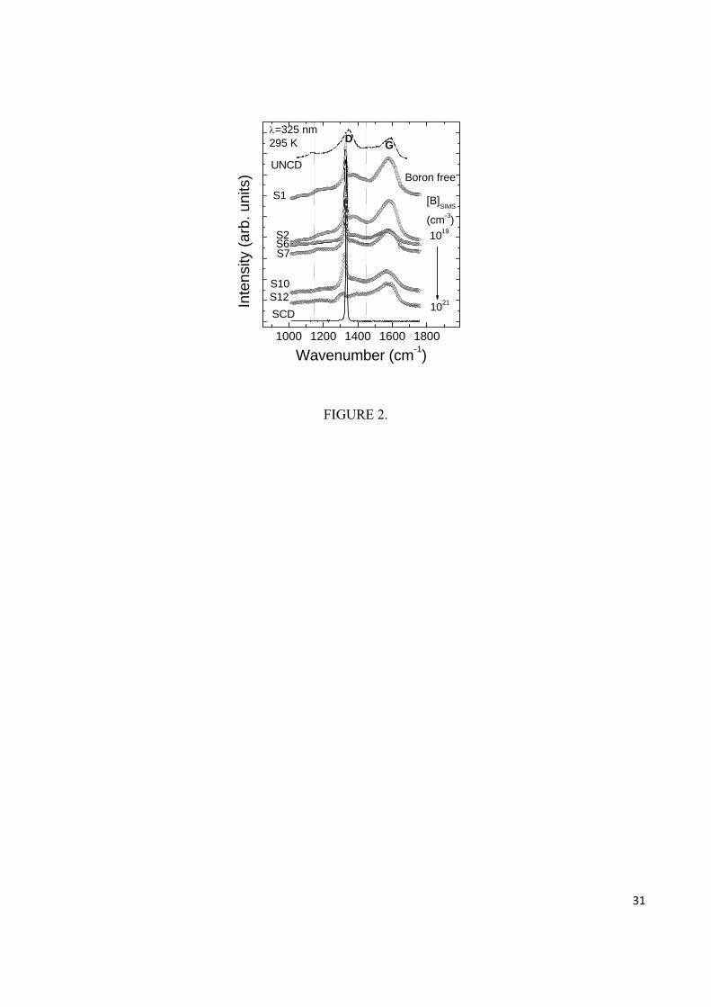
Raman spectroscopy was used to investigate the quality of the diamond films. Typical Raman spectra
of the NCD films are presented in Fig. 2 together with the spectra of one undoped single crystalline
diamond film and one nitrogen-free UNCD film. The spectra of the NCD films are comparable to those
obtained by other authors.33-35 Typically, in addition to the first order diamond peak at 1332 cm-1, the D
(expected at 1350 cm-1)35 and G (expected at 1600 cm-1)35 bands related to sp2 carbon are visible due to
the contribution of grain boundaries in the NCD material. The position of the first order diamond peak
shifts slightly from the 1332.5 cm-1 position in natural diamond35 towards lower wavenumbers (see Fig.
3 for details). There are two main reasons which could explain the shift: the influence of doping and the
influence of the grain size. The influence of boron doping on the diamond first order Raman line has
7
been well characterized for single and polycrystalline diamond films, and it has been explained by the
Fano-type interference between the continuum of electronic states introduced by the dopants and the
discrete zone centre phonon.33-35,41
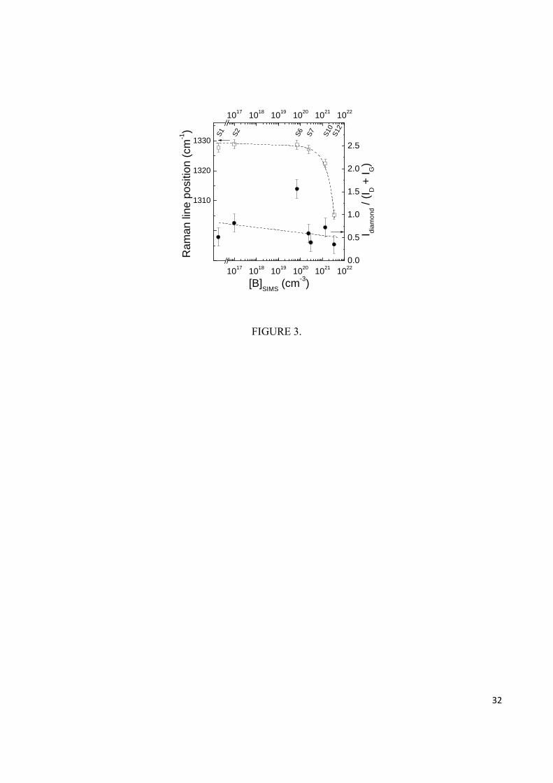
The most pronounced effect was observed for films with boron concentration higher than 1020 cm-3,
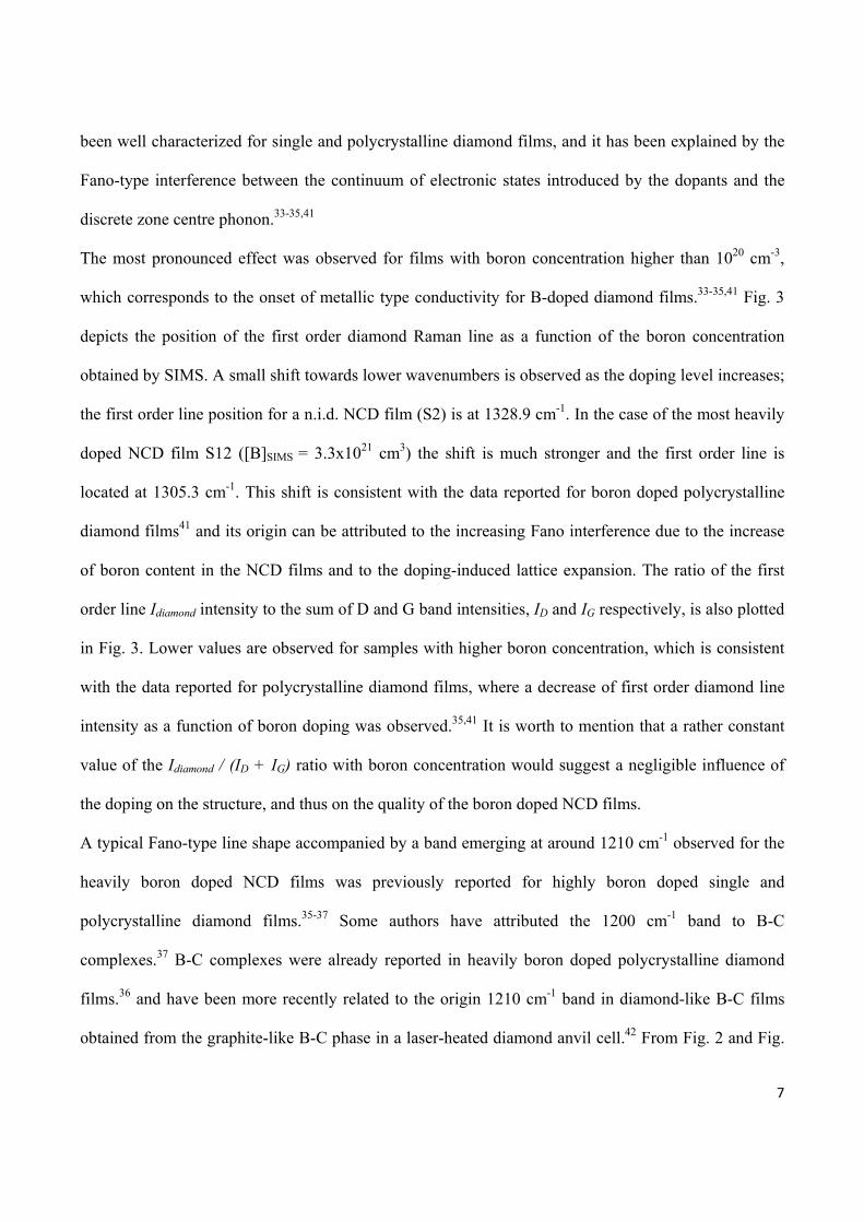
which corresponds to the onset of metallic type conductivity for B-doped diamond films.33-35,41 Fig. 3
depicts the position of the first order diamond Raman line as a function of the boron concentration
obtained by SIMS. A small shift towards lower wavenumbers is observed as the doping level increases;
the first order line position for a n.i.d. NCD film (S2) is at 1328.9 cm-1. In the case of the most heavily
doped NCD film S12 ([B]SIMS = 3.3x1021 cm3) the shift is much stronger and the first order line is
located at 1305.3 cm-1. This shift is consistent with the data reported for boron doped polycrystalline
diamond films41 and its origin can be attributed to the increasing Fano interference due to the increase
of boron content in the NCD films and to the doping-induced lattice expansion. The ratio of the first
order line Idiamond intensity to the sum of D and G band intensities, ID and IG respectively, is also plotted
in Fig. 3. Lower values are observed for samples with higher boron concentration, which is consistent
with the data reported for polycrystalline diamond films, where a decrease of first order diamond line
intensity as a function of boron doping was observed.35,41 It is worth to mention that a rather constant
value of the Idiamond / (ID + IG) ratio with boron concentration would suggest a negligible influence of
the doping on the structure, and thus on the quality of the boron doped NCD films.
A typical Fano-type line shape accompanied by a band emerging at around 1210 cm-1 observed for the
heavily boron doped NCD films was previously reported for highly boron doped single and
polycrystalline diamond films.35-37 Some authors have attributed the 1200 cm-1 band to B-C
complexes.37 B-C complexes were already reported in heavily boron doped polycrystalline diamond
films.36 and have been more recently related to the origin 1210 cm-1 band in diamond-like B-C films
obtained from the graphite-like B-C phase in a laser-heated diamond anvil cell.42 From Fig. 2 and Fig.
8
3 it can be concluded that the intensity of the G and D bands is significantly lower in NCD than in
UNCD, indicating lower sp2 content in NCD films. This is not surprising, since the density of grain
boundaries in UNCD is larger due to the smaller grain size.14,32 Grain boundaries were already
suggested to have a strong influence on Raman characterization as well as in the electronic properties
of UNCD films.32 As in the case of the first order diamond line, both the D and G bands shifts slightly
towards lower wavenumbers with the increase of the boron doping level. For the G band, this shift
could suggest a slow increase of the bond disorder,34 which could be tentatively assigned to the
presence of boron in the grain boundaries. Two peaks around 1150 cm-1 and 1450 cm-1 are detected
only in NCD and UNCD films, and have been attributed to the presence of hydrocarbon layers. The
visible Raman spectroscopy (514.5 nm, not shown in the graph) reveals both 1150 cm-1 and 1450 cm-1
peaks, although they are slightly shifted to lower and to higher wavenumbers, respectively. For the
NCD film with the highest boron doping both peaks are hardly visible, which could be the result of a
lower H incorporation in the grain boundaries.
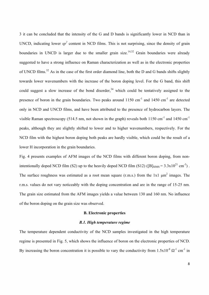
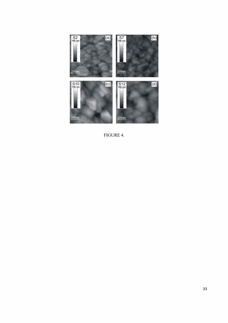
Fig. 4 presents examples of AFM images of the NCD films with different boron doping, from non-
intentionally doped NCD film (S2) up to the heavily doped NCD film (S12) ([B]SIMS = 3.3x1021 cm-3) .
The surface roughness was estimated as a root mean square (r.m.s.) from the 1x1 μm2 images. The
r.m.s. values do not vary noticeably with the doping concentration and are in the range of 15-25 nm.
The grain size estimated from the AFM images yields a value between 130 and 160 nm. No influence
of the boron doping on the grain size was observed.
B. Electronic properties
B.1. High temperature regime
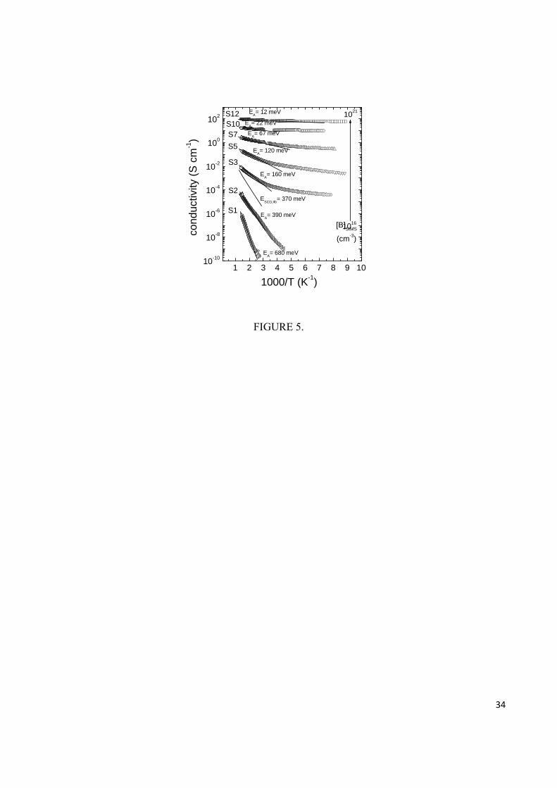
The temperature dependent conductivity of the NCD samples investigated in the high temperature
regime is presented in Fig. 5, which shows the influence of boron on the electronic properties of NCD.
By increasing the boron concentration it is possible to vary the conductivity from 1.5x10⁻⁸ Ω-1 cm-1 in
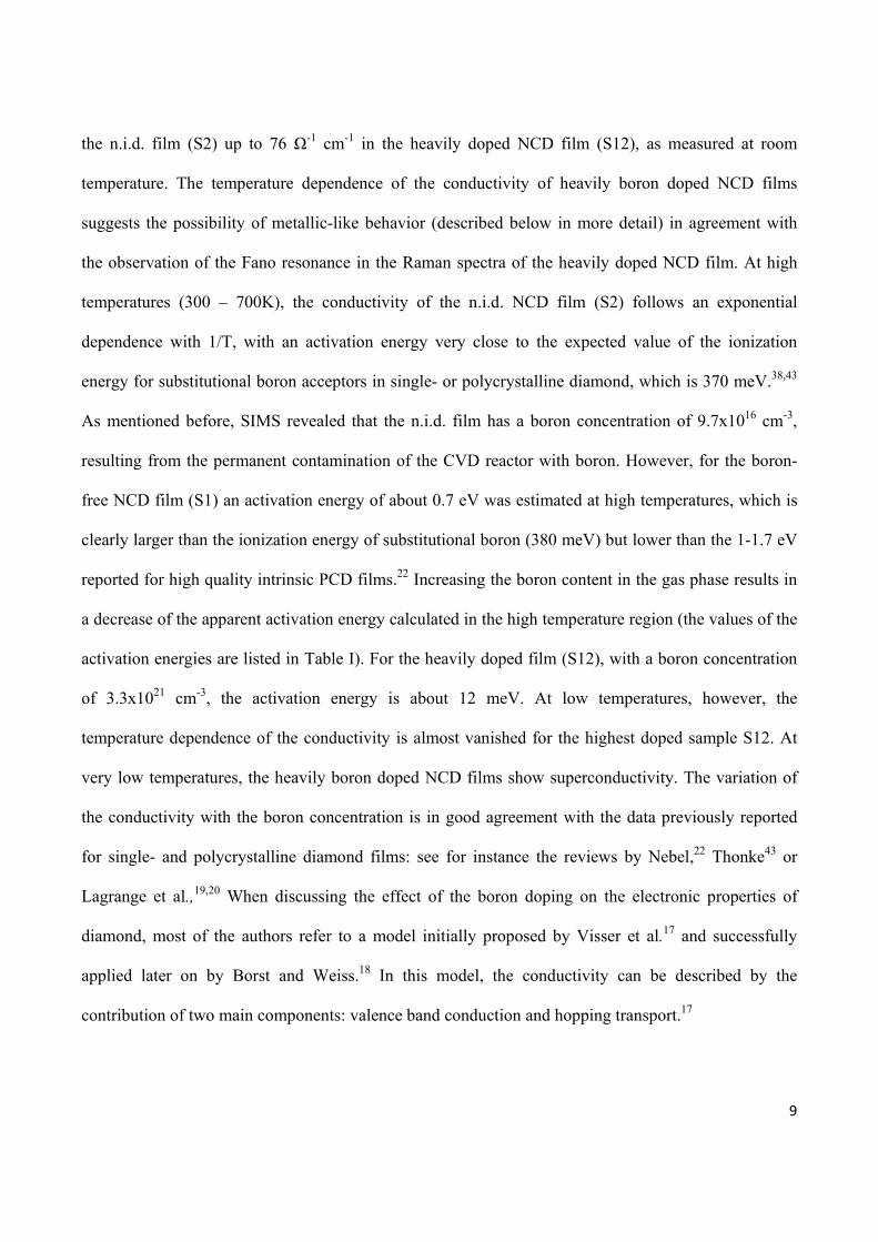
9
the n.i.d. film (S2) up to 76 Ω-1 cm-1 in the heavily doped NCD film (S12), as measured at room
temperature. The temperature dependence of the conductivity of heavily boron doped NCD films
suggests the possibility of metallic-like behavior (described below in more detail) in agreement with
the observation of the Fano resonance in the Raman spectra of the heavily doped NCD film. At high
temperatures (300 – 700K), the conductivity of the n.i.d. NCD film (S2) follows an exponential
dependence with 1/T, with an activation energy very close to the expected value of the ionization
energy for substitutional boron acceptors in single- or polycrystalline diamond, which is 370 meV.38,43
As mentioned before, SIMS revealed that the n.i.d. film has a boron concentration of 9.7x1016 cm-3,
resulting from the permanent contamination of the CVD reactor with boron. However, for the boron-
free NCD film (S1) an activation energy of about 0.7 eV was estimated at high temperatures, which is
clearly larger than the ionization energy of substitutional boron (380 meV) but lower than the 1-1.7 eV
reported for high quality intrinsic PCD films.22 Increasing the boron content in the gas phase results in
a decrease of the apparent activation energy calculated in the high temperature region (the values of the
activation energies are listed in Table I). For the heavily doped film (S12), with a boron concentration
of 3.3x1021 cm-3, the activation energy is about 12 meV. At low temperatures, however, the
temperature dependence of the conductivity is almost vanished for the highest doped sample S12. At
very low temperatures, the heavily boron doped NCD films show superconductivity. The variation of
the conductivity with the boron concentration is in good agreement with the data previously reported
for single- and polycrystalline diamond films: see for instance the reviews by Nebel,22 Thonke43 or
Lagrange et al.,19,20 When discussing the effect of the boron doping on the electronic properties of
diamond, most of the authors refer to a model initially proposed by Visser et al.17 and successfully
applied later on by Borst and Weiss.18 In this model, the conductivity can be described by the
contribution of two main components: valence band conduction and hopping transport.17
10
Motion of holes in extended states of the valence band represents the typical transport mechanism of a
p-type semiconductor at high temperature. If a certain degree of compensation is present, the activation
energy is determined by the ionization energy of the acceptor (for boron in diamond, EA = 370 meV).
This situation, however, is only valid for weakly boron–doped NCD films. For instance, the apparent
activation energy of the temperature-dependent conductivity of the n.i.d film (S2) is EA = 390 meV. As
the boron concentration increases, the activation energy calculated in the high temperature range (from
295 up to 700K) decreases down to 12 meV for heavily doped NCD films. The observed trend is
consistent with the expected metal-insulator transition (Mott transition), which in the case of
polycrystalline diamond films is expected for a boron concentration between 1020-1021 cm-3.36
The activation energy decrease with doping was originally discussed for silicon by Pearson and
Bardeen,44 who proposed the following dependence of the effective activation energy on dopant
concentration, NA:
( ) 31AIAeff NEE α−= (1)
where EI corresponds to the ionization energy for an isolated impurity center and α is a constant which
was determined theoretically.44 This model was applied to diamond by Lagrange and Thonke,19,20,43
using EI = 370 meV for substitutional boron; for the case of diamond, the proportionality factor α
calculated theoretically is 6.7 x 10⁻⁸ eV/cm. Although a qualitative agreement with the experimental
data was obtained, this model was not able to fully explain the experiments. The discussion of Pearson
and Bardeen was later on modified by Lee and McGill.45 It was shown that at least three other
mechanisms should be considered to correctly account for the concentration dependence of the
activation energy: the broadening of the impurity level, the tailing of the band edge, and the shift of the
band edge.45 The broadening of the impurity level was demonstrated to be the most important term, and
is induced by the overlap between the impurity wave functions. This overlapping is proportional to the
11
mean distance between the impurities, and thus proportional to (NA)-1/3. Thus, the prediction of the Lee
and McGill model closely resembles the dependence given in Eq. (1).
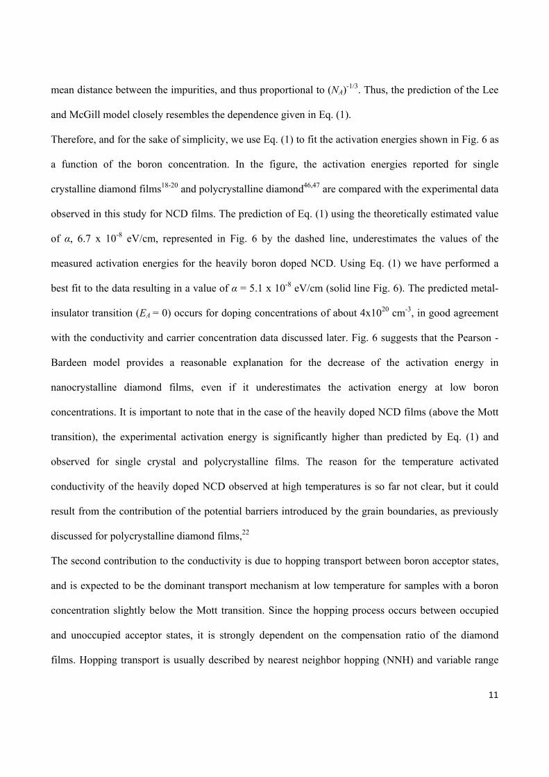
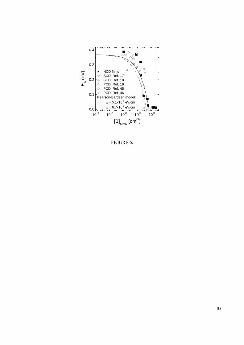
Therefore, and for the sake of simplicity, we use Eq. (1) to fit the activation energies shown in Fig. 6 as
a function of the boron concentration. In the figure, the activation energies reported for single
crystalline diamond films18-20 and polycrystalline diamond46,47 are compared with the experimental data
observed in this study for NCD films. The prediction of Eq. (1) using the theoretically estimated value
of α, 6.7 x 10⁻⁸ eV/cm, represented in Fig. 6 by the dashed line, underestimates the values of the
measured activation energies for the heavily boron doped NCD. Using Eq. (1) we have performed a
best fit to the data resulting in a value of α = 5.1 x 10⁻⁸ eV/cm (solid line Fig. 6). The predicted metal-
insulator transition (EA = 0) occurs for doping concentrations of about 4x1020 cm-3, in good agreement
with the conductivity and carrier concentration data discussed later. Fig. 6 suggests that the Pearson -
Bardeen model provides a reasonable explanation for the decrease of the activation energy in
nanocrystalline diamond films, even if it underestimates the activation energy at low boron
concentrations. It is important to note that in the case of the heavily doped NCD films (above the Mott
transition), the experimental activation energy is significantly higher than predicted by Eq. (1) and
observed for single crystal and polycrystalline films. The reason for the temperature activated
conductivity of the heavily doped NCD observed at high temperatures is so far not clear, but it could
result from the contribution of the potential barriers introduced by the grain boundaries, as previously
discussed for polycrystalline diamond films,22
The second contribution to the conductivity is due to hopping transport between boron acceptor states,
and is expected to be the dominant transport mechanism at low temperature for samples with a boron
concentration slightly below the Mott transition. Since the hopping process occurs between occupied
and unoccupied acceptor states, it is strongly dependent on the compensation ratio of the diamond
films. Hopping transport is usually described by nearest neighbor hopping (NNH) and variable range
12
hopping (VRH). Both are expected to be strongly dependent on the distance between the acceptor
atoms.18,48 In the case of diamond, the boron acceptor activation energy is relatively high, enabling the
NNH mechanism to be observed even at room temperature. The VRH process was observed in
different diamond films, typically at temperatures lower than 150K.44
We will discuss now a third contribution to the conductivity in NCD, which accounts for the hopping
conduction in the grain boundaries, previously identified in undoped UNCD films as the main
conduction path.15,32 In high quality PCD films, where neither nitrogen nor boron dopants contribute to
conduction, the measured activation energy of the conductivity, EA ~ 1-1.7 eV, was attributed to the
thermal activation of carriers in π-π* bands introduced by sp2-bonded carbon present in the grain
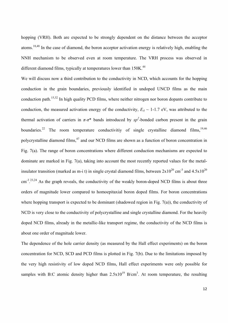
boundaries.22 The room temperature conductivitiy of single crystalline diamond films,19,46
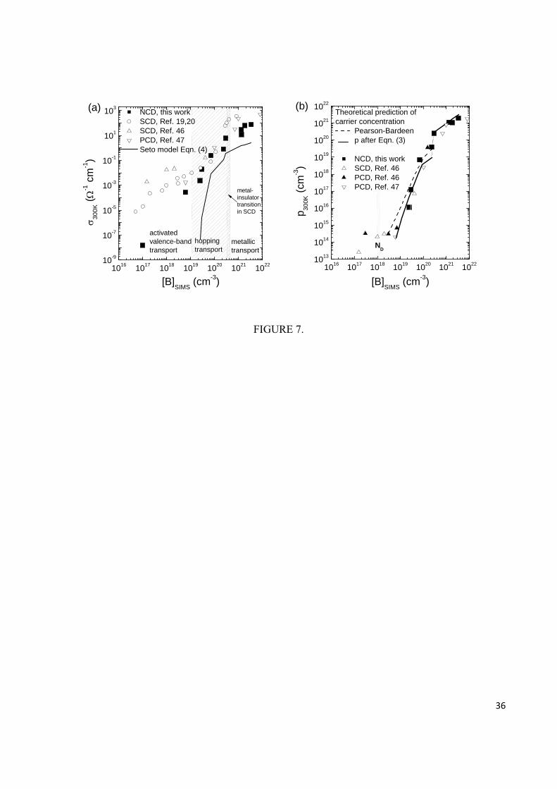
polycrystalline diamond films,47 and our NCD films are shown as a function of boron concentration in
Fig. 7(a). The range of boron concentrations where different conduction mechanisms are expected to
dominate are marked in Fig. 7(a), taking into account the most recently reported values for the metal-
insulator transition (marked as m-i t) in single crystal diamond films, between 2x1020 cm-3 and 4.5x10²⁰
cm-3.23,24 As the graph reveals, the conductivity of the weakly boron-doped NCD films is about three
orders of magnitude lower compared to homoepitaxial boron doped films. For boron concentrations
where hopping transport is expected to be dominant (shadowed region in Fig. 7(a)), the conductivity of
NCD is very close to the conductivity of polycrystalline and single crystalline diamond. For the heavily
doped NCD films, already in the metallic-like transport regime, the conductivity of the NCD films is
about one order of magnitude lower.
The dependence of the hole carrier density (as measured by the Hall effect experiments) on the boron
concentration for NCD, SCD and PCD films is plotted in Fig. 7(b). Due to the limitations imposed by
the very high resistivity of low doped NCD films, Hall effect experiments were only possible for
samples with B:C atomic density higher than 2.5x10¹⁹ B/cm3. At room temperature, the resulting
13
carrier concentration ranges from 7x1015 cm-3 for a weakly doped (S4) film up to 2x1021 cm-3 in the
heavily doped (S12) NCD film. It can be observed that the carrier concentration measured in NCD
films is comparable to the values measured in SCD and PCD diamond. The large scattering of values
observed in Fig. 7(b) can be explained by the uncertainty of the SIMS concentration values as well as
of the carrier concentration calculated from the Hall experiments. The value of the boron concentration
at which the conductivity mechanism changes from hopping conduction to metal-like conduction is
around 4x1020 cm-3, as estimated from Fig. 6 and 7, which is in good agreement with the values
reported for boron-doped SCD diamond films.19,20,23,24
To calculate the expected concentration of holes in NCD, the condition of neutrality for a p-type
diamond with compensation was used together with expression for the hole concentration in a non-
degenerate p-type semiconductor, resulting in:
( )x
B
ABh
DA
D NTk
Eh
TkmpNN
Npp≡⎟⎟
⎠
⎞⎜⎜⎝
⎛−⎟⎟
⎠
⎞⎜⎜⎝
⎛=
−−+ exp2
2/3
2
*π (2)
which yields an expression for the hole density p:
( )( ) ⎟
⎟⎠
⎞⎜⎜⎝
⎛−
+−
++
= 1412 2
XD
DAxxD
NNNNNNNp (3)
where NA is the boron doping, ND the compensating donor density, EA the activation energy of the hole
concentration, and *hm the hole effective mass. A concentration of compensating donors of ND = 1x10¹⁸
cm-3, and eh mm 7.0* = were used for calculations. The carrier concentration for NCD films with low and
intermediate doping calculated according to Eq. (3) are plotted in Fig. 7(b) as a solid line. For the
calculations, we used the activation energy obtained from the fit of the temperature dependence of the
carrier concentration measured with Hall effect, as shown in Fig. 8(a) and discussed below. As can be
seen in Fig. 7(b), within experimental accuracy, the data are in good agreement with the calculated
values corresponding to the lower doping level (films S4, S5) and the intermediate boron-doped NCD
films (S6). In the calculations a constant value of the compensating donors was assumed, which is not
14
necessarily the case: it is possible that for weakly doped NCD films the concentration of the donors,
ND, is higher than assumed. For the heavily doped films (S7-S12) above the metal-insulator transition,
however, an underestimation of the calculated carrier density is expected as a result of the assumption
of a non-degenerate system used to derive Eq. (2) and (3). Thus, for boron concentrations above the
metal-insulator transition, it can be assumed that the number of free carriers corresponds to the number
of impurities, if compensation is negligible. In Fig. 7(b), the solid line shown for boron concentrations
above 3x1020 cm-3 corresponding to the calculated value of the density of holes assuming p=NA, is in
very good agreement with the experimentally determined carrier concentration. The dashed line in Fig.
7(b) was calculated according to Eq. (3) using the EA values of the Pearson-Bardeen model obtained
from Eq. (1) with α = 5.1 x 10⁻⁸ eV/cm. The calculated values are also in good agreement with the
experimental data for boron-doped NCD films below the metal-insulator transition, suggesting that the
Pearson-Bardeen model can be used to predict the increase of the carrier concentration with boron
doping, which results from the lowering of the activation energy due to the decrease of the average
distance between the acceptors.
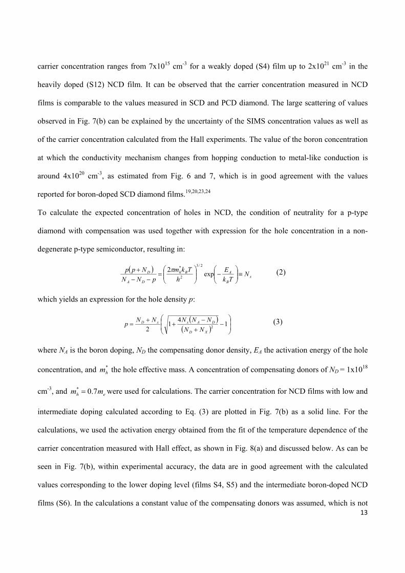
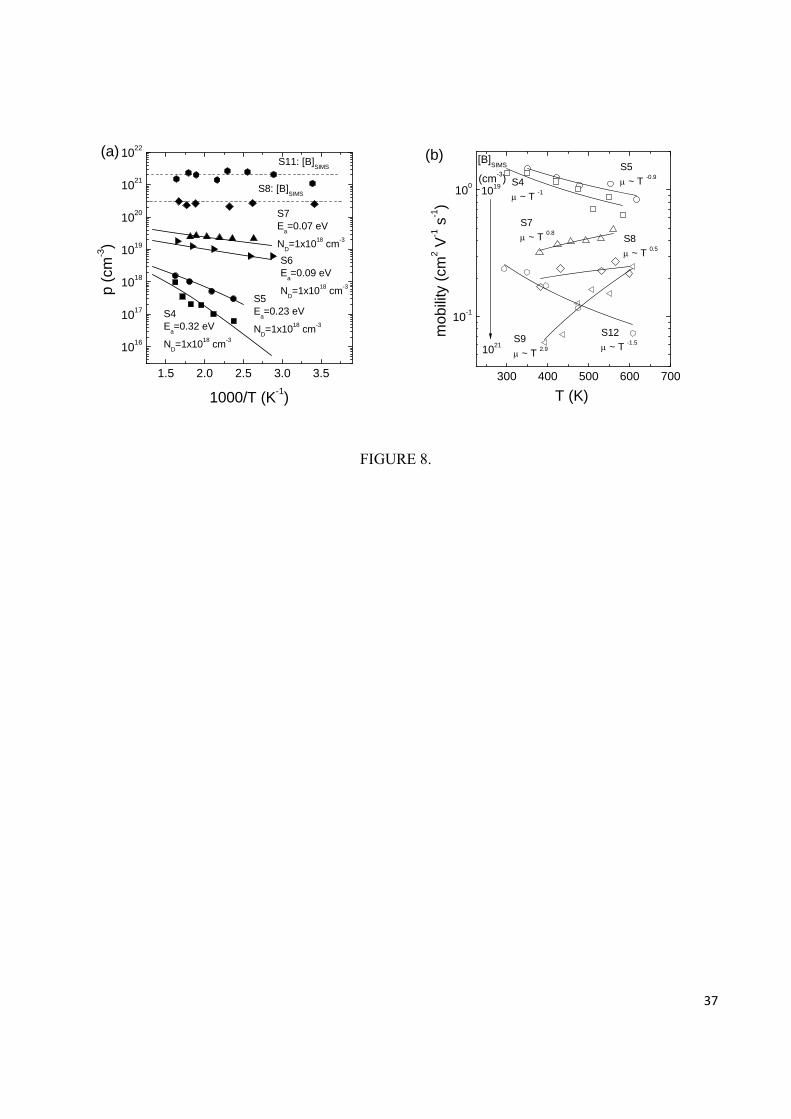
The temperature dependence of the carrier concentration and mobility calculated from Hall-
effect experiments are shown in Fig. 8(a) and Fig. 8(b), for temperatures between 295K and 700K. In
general, heavily doped samples show a weak temperature dependence of the carrier concentration, in
good agreement with the results of the conductivity. Eq. (3) was used to fit the experimental data of
low and intermediate boron-doped NCD films (S4-S7). The fitting parameters are shown in the graph
for each NCD film. For the low doped NCD films S4 and S5, more pronounced temperature
dependence is observed in the high temperature regime, and the activation energy of the carrier
concentration gets closer to 370 meV, as expected for a compensated boron-doped diamond. As
discussed before, for NCD films with boron concentration above the Mott transition (S8-S12) we
assume that p ≈ NA. The experimentally determined carrier concentration for the heavily boron-doped
15
NCD films S8 and S11 is also plotted in Fig. 8(a) together with the boron concentration [B]SIMS
determined by SIMS (dashed lines). A good agreement between the Hall effect data and SIMS is
observed, confirming the expected metal-like behavior of the electronic transport in heavily doped
NCD films.
On the other hand, it is important to determine whether the sp2 amorphous carbon phase of the
grain boundaries contributes or not to the conduction process of the heavily doped sample, as is the
case for ultrananocrystalline diamond films.32 In UNCD films the conductivity has been attributed to
the presence of sp2 carbon in the grain boundaries which increases with the amount of nitrogen in the
gas phase.15,16 Thus, it has been shown that electron transport occurs in a defect band at the grain
boundaries. In contrast, our Hall effect experiments confirm that in the B-doped NCD films the
conductivity is due to holes and not electrons, suggesting that electronic transport in the grain
boundaries is not an important transport mechanism in B-doped NCD. In addition, from the analysis of
the Raman data (Fig. 2) we have concluded that the amorphous carbon content does not increase
significantly with the boron concentration, and therefore its contribution to the conductivity of heavily
doped NCD can be neglected. Figure 8(b) shows the temperature dependence of the hole mobility, as
calculated from the Hall effect experiments. The mobility values are roughly one to two orders of
magnitude lower than the mobility of single crystal diamond films with comparable doping levels, so
that additional scattering mechanisms dominate over the basic mechanisms like impurity scattering and
phonon scattering. The lines in Fig. 8(b) correspond to best fits of the temperature-dependent mobility
using γμ T∝ . The values of the exponent γ are shown in Figure 8(b). The expected temperature
dependence of the mobility for acoustic phonon scattering is 2/3−∝ Tμ and for ionized impurities
scattering 2/3T∝μ .50 From Fig. 8(b), it is evident that the interpretation of the temperature-dependent
mobility data is rather difficult, and a reliable conclusion on the dominant scattering mechanism is not
possible.
16
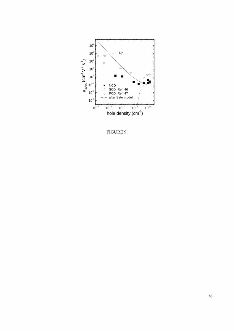
In order to verify the possible influence of the grain boundary scattering and ionized acceptor
scattering on the free carrier mobility the experimental data at room temperature have been plotted in
Fig. 9 as a function of boron concentration, together with the theoretical predictions of ionized impurity
scattering and grain boundary scattering expected for polycrystalline material.49 The carrier mobility
dependence on boron doping for single crystalline46 and polycrystalline47 diamond films have also been
plotted in Fig. 9 for comparison. The hole mobility decreases with doping, from 2 cm2V-1s-1 in a low
boron doped sample (S4) to 0.2 cm2V-1s-1 in the highest doped sample (S12). The observed decrease of
the carrier mobility with increasing boron concentration is qualitatively consistent with the behavior of
single- and polycrystalline diamond films.20,22,18 However, due to the nanocrystalline structure of NCD
films, the scattering at the grain boundaries is expected to be the main cause of the relatively low hole
mobility measured for the low B-doped NCD films. For comparison, in weakly doped polycrystalline
diamond films (hole density in the range of 4x1015 cm-3), the hole mobility is close to 40 cm2V-1s-1.22
Compared to single crystalline diamond with the same boron concentration, the mobility in NCD is of
three orders of magnitude lower. For the NCD film S4 with hole density in the range of 1015 cm-3 the
mobility is about 2 cm2V-1s-1. For increasing boron concentration, however, the mobility of SCD, PCD,
and NCD get closer. We have considered the influence of the grain boundaries within the Seto model,
which was originally introduced to explain the electronic transport of B-doped micro- and
nanocrystalline silicon.49 Charge trapping at grain boundaries, which leads to the formation of potential
barriers, is responsible for the measured high activation energies (much higher than expected for
substitutional boron acceptors in Si) in polycrystalline silicon films.49 For a given crystallite size (L), a
critical value of boron doping NAc must be exceeded to prevent the crystal regions from total depletion
of carriers. This results in an abrupt increase of free carrier density and conductivity of the
polycrystalline silicon films at NAc. The carrier mobility estimated by Seto is given by:49
17
⎥⎦
⎤⎢⎣
⎡ −⎟⎟⎠
⎞⎜⎜⎝
⎛=
TNkqQ
TkmLq
ABBha επ
μ8
exp2
1 221
* (4)
where Q corresponds to the density of traps in the grain boundaries. Using L = 150 nm and Q = 5x10¹³
cm-2, and a hole effective mass eh mm 7.0* = ,18 the prediction of Eq. (4) is plotted in Fig. 9 as a dashed
line. Should the mobility be exclusively dependent on the potential barriers introduced by the grain
boundaries, as modeled by Seto, a minimum of the mobility would be expected at NAc.49 From the
experimental data of the B-doped NCD films no such a mobility minimum is observed. On the other
hand, the decrease of the carrier mobility observed for NCD films stays in reasonable agreement with
the expected mobility lowering as a result of the ionized acceptors scattering. The solid line in Fig. 9
corresponds to the mobility calculated assuming ionized impurity scattering using:50
( )12
3/120
2/1*3
2/320 121ln264
−
⎪⎭
⎪⎬⎫
⎪⎩
⎪⎨⎧
⎥⎥⎦
⎤
⎢⎢⎣
⎡⎟⎟⎠
⎞⎜⎜⎝
⎛+=
pqkT
mpqkT
h
ionizedπεεπμ (5)
in which a density of ionized impurities, p, calculated using Eqn. (3), ε0 = 5.7 and an effective hole
mass of eh mm 7.0* = were used. It can be seen that the decrease of the mobility in SCD and PCD films
(Ref. 22 and references therein) also follow the trend predicted by Eq. (5).
In addition, the conductivity calculated using the Seto model (dashed line in Fig. 7(a)) predicts a sharp
decrease of conductivity which does not correspond to the experimental data. The disagreement of the
carrier mobility and conductivity values calculated using the Seto model with the experimental data can
have several reasons: i) too large size of the diamond crystallites (L>100nm) for which the Seto model
fails,46 and ii) the Seto assumption of a full acceptors ionization p=NA, which in the case of boron-
doped NCD films with a relatively high acceptor ionization energy and weak compensation is not valid.
Alternatively, a modified Seto model could be used (Ref. 46 and references therein) taking into account
carrier scattering processes depending on the ratio between the grain size and the carrier depletion
region size. From our experimental data it is not possible to perform a more detailed study of the
18
influence of the grain boundary trapping on the electronic properties of B-doped NCD films. It would
be necessary to perform a comprehensive study of the electronic properties of NCD films with low and
intermediate boron doping as well as with smaller grain size in order to investigate a possible influence
of the charge trapping effect induced by the grain boundaries. Currently, we can not rule out the effect
of charge trapping at grain boundaries at low boron-doping levels, below 1018 cm-3.
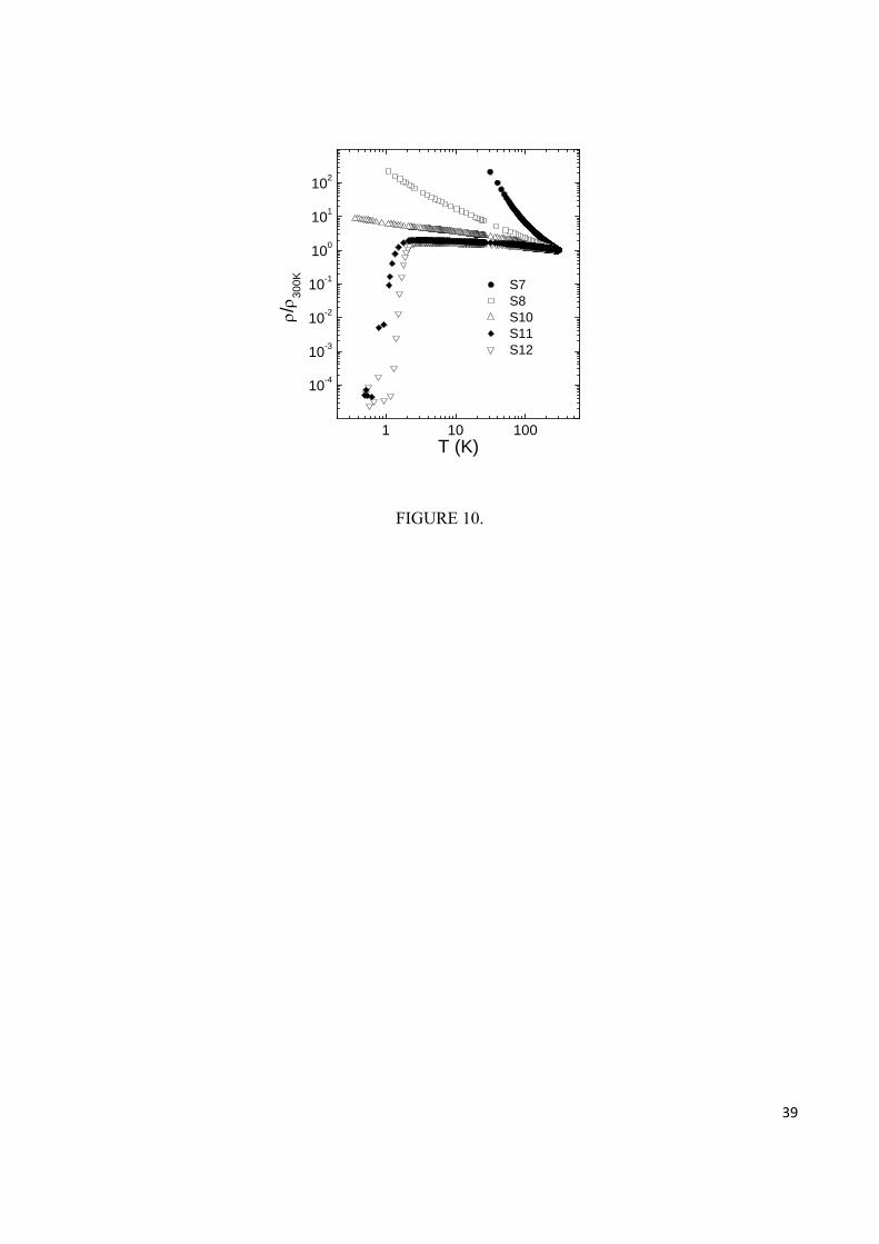
B.2 Low temperature regime
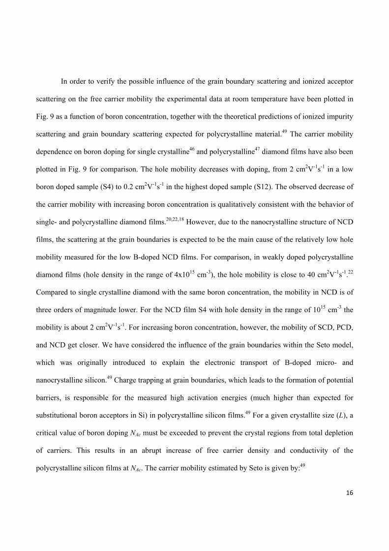
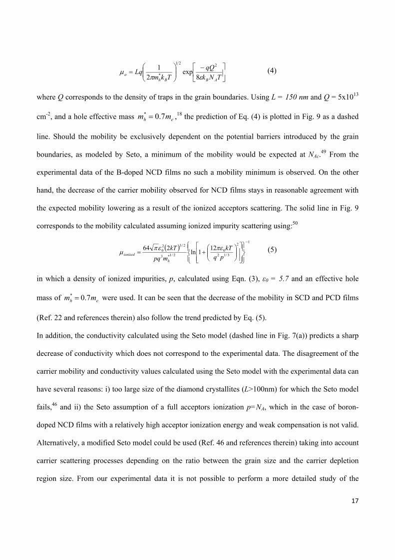
The temperature dependence of the normalized resistance ρ/ρ(300K) in the range 300 K down to 350
mK is shown in Fig. 10 for several samples. In contrast to the minimum resistivity observed in single
crystal diamond at intermediate temperatures24, the resistivity of nanocrystalline diamond increases
with decreasing temperature. The highly doped samples with nB ≥ 1.3× 1021cm−3 also show
superconductivity with a critical temperatures of about Tc = 2.1 K (Samples S8 and S10 behaved like a
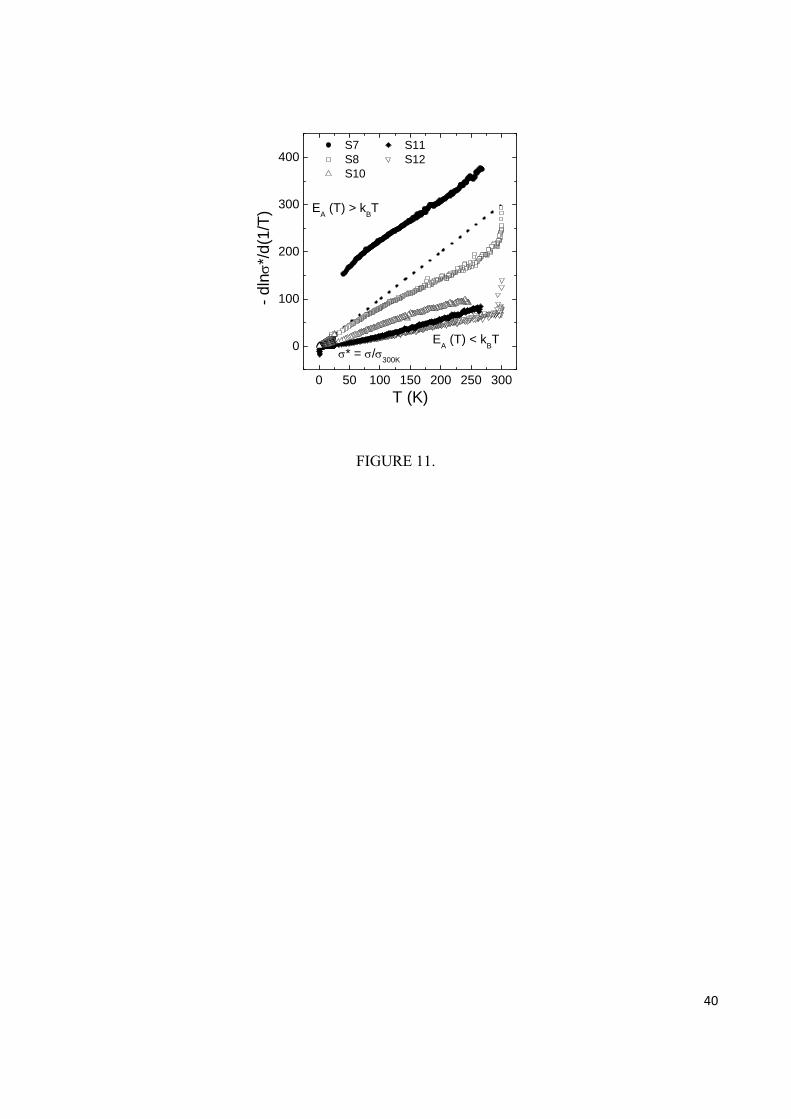
disordered metal, but showed no superconductivity down to 350 mK). Fig. 11 shows the effective
activation energy Eact as determined from the slope of Arrhenius plots of the temperature dependent
conductivity σ*, normalized to its room temperature value. As mentioned in the previous section,
thermally activated transport via hopping conduction (Eact > kBT) is only observed for the weakly
doped sample S7. In contrast to the classical behavior of an insulator, the apparent activation energy of
a metal is only a small fraction of kBT in the corresponding temperature range, as already reported
elsewhere51 - 53. The highly-doped samples behave like a disordered metal (Eact < kBT). Therefore, the
critical boron concentration nc for the metal-insulator transition, as obtained from the low temperature
experiments, lies in the range from 2.3×1020 cm−3 up to 2.9 × 1020 cm−3, in good agreement with the
results discussed in previous sections, and with what was found for single crystal and polycrystalline
diamond (Ref. 54,55). Due to the granularity of the diamond thin film, we expect that the metal-
insulator transition is not only due to the increasing doping within the grains, but also to the increase in
intergranular coupling between metallic grains.
19
C. Optical properties
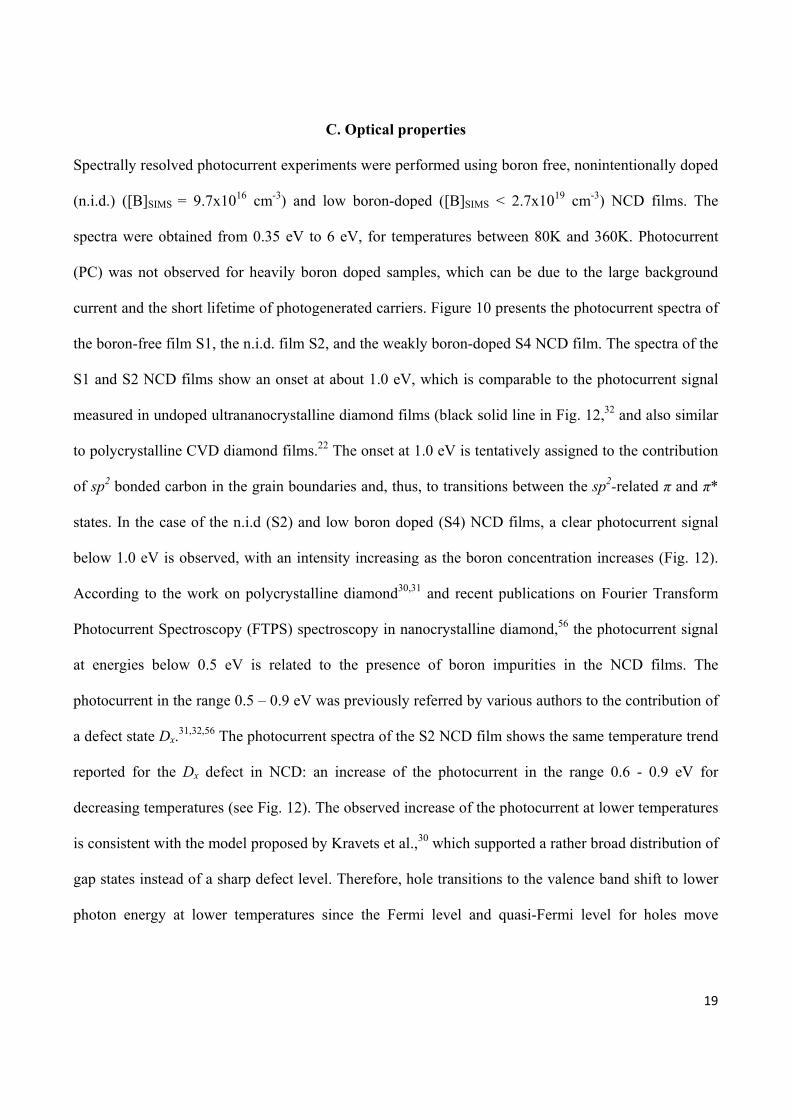
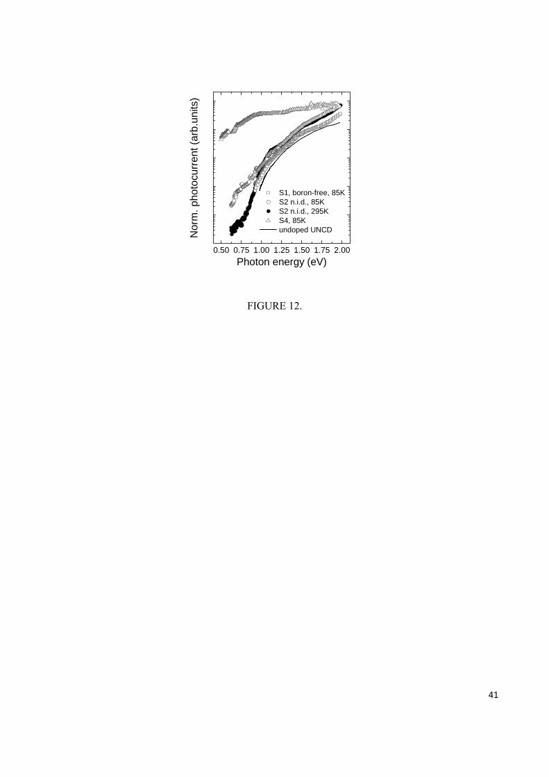
Spectrally resolved photocurrent experiments were performed using boron free, nonintentionally doped
(n.i.d.) ([B]SIMS = 9.7x1016 cm-3) and low boron-doped ([B]SIMS < 2.7x1019 cm-3) NCD films. The
spectra were obtained from 0.35 eV to 6 eV, for temperatures between 80K and 360K. Photocurrent
(PC) was not observed for heavily boron doped samples, which can be due to the large background
current and the short lifetime of photogenerated carriers. Figure 10 presents the photocurrent spectra of
the boron-free film S1, the n.i.d. film S2, and the weakly boron-doped S4 NCD film. The spectra of the
S1 and S2 NCD films show an onset at about 1.0 eV, which is comparable to the photocurrent signal
measured in undoped ultrananocrystalline diamond films (black solid line in Fig. 12,32 and also similar
to polycrystalline CVD diamond films.22 The onset at 1.0 eV is tentatively assigned to the contribution
of sp2 bonded carbon in the grain boundaries and, thus, to transitions between the sp2-related π and π*
states. In the case of the n.i.d (S2) and low boron doped (S4) NCD films, a clear photocurrent signal
below 1.0 eV is observed, with an intensity increasing as the boron concentration increases (Fig. 12).
According to the work on polycrystalline diamond30,31 and recent publications on Fourier Transform
Photocurrent Spectroscopy (FTPS) spectroscopy in nanocrystalline diamond,56 the photocurrent signal
at energies below 0.5 eV is related to the presence of boron impurities in the NCD films. The
photocurrent in the range 0.5 – 0.9 eV was previously referred by various authors to the contribution of
a defect state Dx.31,32,56 The photocurrent spectra of the S2 NCD film shows the same temperature trend
reported for the Dx defect in NCD: an increase of the photocurrent in the range 0.6 - 0.9 eV for
decreasing temperatures (see Fig. 12). The observed increase of the photocurrent at lower temperatures
is consistent with the model proposed by Kravets et al.,30 which supported a rather broad distribution of
gap states instead of a sharp defect level. Therefore, hole transitions to the valence band shift to lower
photon energy at lower temperatures since the Fermi level and quasi-Fermi level for holes move
20
towards the valence band edge with decreasing temperature.30 However, the origin of this Dx defect is
not understood and, thus, further investigation is required.
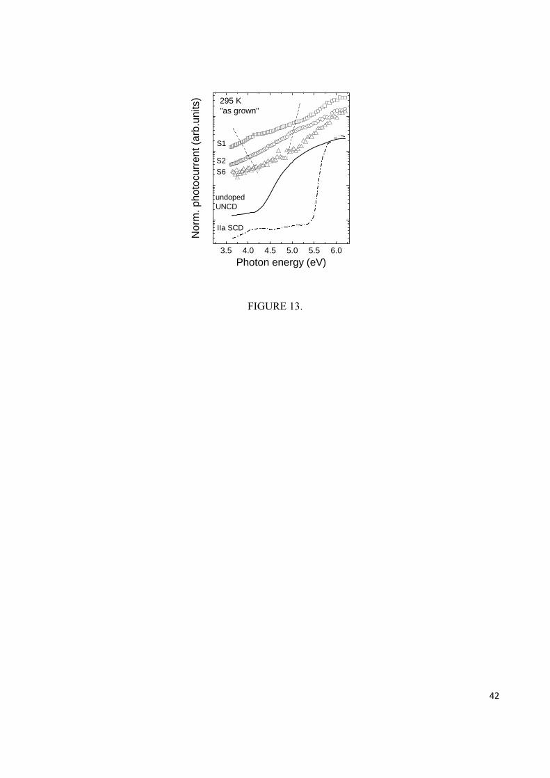
In the high energy range of the spectra two onsets can be observed (Fig. 13), at about 4.0 eV and 5.3
eV. The one at higher energy can be attributed to the indirect band to band transition of diamond. For
NCD films with higher boron doping concentration this transition slightly shifts to lower energies: for
instance, the onset occurs at about 5.0eV for sample S6, with [B]SIMS = 6.9x1019 cm-3. As shown in
Fig. 13, the band to band transition for NCD films is not very pronounced, which is the result of the
high photocurrent at lower energies, as discussed before. As it has been suggested for
polycrystalline22,57 and ultrananocrystalline32 diamond films, the non-diamond phase in the grain
boundaries has a prominent influence on the optical absorption in diamond. For instance, it has been
shown that the grain boundaries play a major role in the photocurrent of UNCD films.32 The PC
spectrum of an undoped UNCD film is shown together with the NCD spectra in Fig. 13. In the UNCD
film, the onset at about 4.1 eV was assigned to transitions between valence and conduction band tails,
which are induced by the disordered sp3 phase.32 For comparison, the photocurrent spectrum of a single
crystalline diamond film (Fig. 13), in which the density of grain boundaries is much lower, shows a
sharp band-to-band absorption onset at about 5.4 eV.
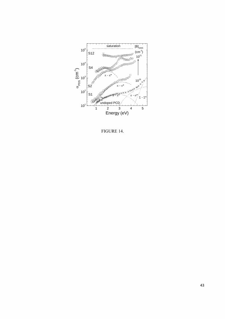
In order to determine the optical absorption coefficient αopt of boron-doped NCD films, photothermal
deflection spectroscopy (PDS) measurements were performed with the boron-free (S1), non-
intentionally doped (S2, [B]SIMS: 9.7x1016 cm-3), weakly boron-doped (S5, [B]SIMS < 2.7x1019 cm-3),
and heavily boron doped (S12, [B]SIMS: 3.34x1021 cm-3) NCD films. The calculated absorption
coefficient is plotted in Fig. 14. We assume a similar energy dependence of the density of states (DOS)
than that used for polycrystalline diamond films22,57 and undoped and nitrogen doped NCD and
UNCD.32 Thus, bonding and anti-bonding, π and π*, sp2-related states as well as dangling bonds
introduced by the grain boundaries, all with a Gaussian shaped distribution,22,57 are expected to bring
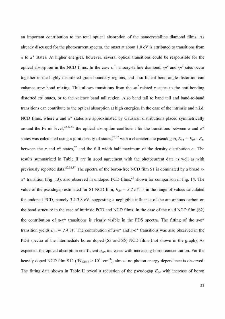
21
an important contribution to the total optical absorption of the nanocrystalline diamond films. As
already discussed for the photocurrent spectra, the onset at about 1.0 eV is attributed to transitions from
π to π* states. At higher energies, however, several optical transitions could be responsible for the
optical absorption in the NCD films. In the case of nanocrystalline diamond, sp2 and sp3 sites occur
together in the highly disordered grain boundary regions, and a sufficient bond angle distortion can
enhance π−σ bond mixing. This allows transitions from the sp2-related π states to the anti-bonding
distorted sp3 states, or to the valence band tail region. Also band tail to band tail and band-to-band
transitions can contribute to the optical absorption at high energies. In the case of the intrinsic and n.i.d.
NCD films, where π and π* states are approximated by Gaussian distributions placed symmetrically
around the Fermi level,22,32,57 the optical absorption coefficient for the transitions between π and π*
states was calculated using a joint density of states,22,32 with a characteristic pseudogap, EΔπ = Eπ* - Eπ,
between the π and π* states,32 and the full width half maximum of the density distribution ω. The
results summarized in Table II are in good agreement with the photocurrent data as well as with
previously reported data.22,32,57 The spectra of the boron-free NCD film S1 is dominated by a broad π-
π* transition (Fig. 13), also observed in undoped PCD films,23 shown for comparison in Fig. 14. The
value of the pseudogap estimated for S1 NCD film, EΔπ = 3.2 eV, is in the range of values calculated
for undoped PCD, namely 3.4-3.8 eV, suggesting a negligible influence of the amorphous carbon on
the band structure in the case of intrinsic PCD and NCD films. In the case of the n.i.d NCD film (S2)
the contribution of π-π* transitions is clearly visible in the PDS spectra. The fitting of the π-π*
transition yields EΔπ = 2.4 eV. The contribution of π-π* and π-σ* transitions was also observed in the
PDS spectra of the intermediate boron doped (S3 and S5) NCD films (not shown in the graph). As
expected, the optical absorption coefficient αopt increases with increasing boron concentration. For the
heavily doped NCD film S12 ([B]SIMS > 1021 cm-3), almost no photon energy dependence is observed.
The fitting data shown in Table II reveal a reduction of the pseudogap EΔπ with increase of boron
22
content. Graphitization of the NCD films could explain the reduction of the pseudogap EΔπ. Raman
spectroscopy, however, did not provide a clear evidence for changes of the D and G bands intensity and
position with increasing boron concentration (Fig. 2). In fact, the intensity ratio Idiamond / (ID + IG) (Fig.
3) was almost independent on the doping level. On the other hand, the contribution of boron acceptors
to the optical absorption in the low energy range of the spectrum could result into an apparent reduction
of the pseudogap EΔπ. Thus, we can conclude that the influence of the boron acceptor on the absorption
coefficient at low energies range is very important, in good agreement with the photocurrent data.
Due to limitations of our PDS setup, we are not able to investigate the optical absorption coefficient at
energy higher than 4.25 eV. Taking into account the photocurrent data, transitions from π states to the
valence band tail region and band tail to band tail transitions are expected to dominate the absorption
processes at high energies, as in the case of the undoped PCD films.22 It is therefore, important to point
out that calculated values of the optical absorption coefficient are comparable to the values obtained by
Achatz et al.32 in nitrogen-free and nitrogen doped UNCD films, confirming that the optical absorption
processes in nanocrystalline diamond films are dominated by the grain boundaries.
IV. CONCLUSIONS
In this work we have studied the structural, electronic and optical properties of boron-doped
nanocrystalline diamond films. Raman spectroscopy was used to investigate the diamond quality of the
films, confirming that the relative amount of amorphous carbon (G and D bands in Raman spectra)
does not change significantly with increasing boron concentration. The electronic properties of B-
doped NCD are controlled by the concentration of boron acceptors in the films. A change of the boron
concentration by five orders of magnitude results in a change of conductivity of almost ten orders of
magnitude, from 1.5x10⁻⁸ Ω-1cm-1 for non-intentionally boron doped film ([B]SIMS = 9.7x1016 cm-3) up
to 76 Ω-1cm-1 for heavily B-doped ([B]SIMS = 3.3x1021 cm-3). The carrier concentration for low and
intermediate doped samples is thermally activated in the temperature range from 300K to 700K, with
23
an activation energy decreasing with increasing boron concentration. The doping dependence of the
activation energy was modeled using a quasi-phenomenological relationship proposed by Pearson and
Bardeen,44 which can result from the combination of different effects such as impurity level broadening
and the electrostatic interaction between free carriers and ionized impurities. At higher boron doping
([B]SIMS > 1.3x1020 cm-3), the conductivity and the carrier concentration show very weak temperature
dependence, and the samples exhibit metal-like properties, with the carrier concentration measured by
Hall effect equal to the concentration of boron in the films. The mobility of the investigated NCD films
decreases with increasing boron concentration, resembling the behavior expected for ionized impurity
scattering: at low boron doping ([B]SIMS = 2.7x1019 cm-3) the mobility is 2.1 cm2V-1s-1, while at high
boron doping ([B]SIMS = 3.3x1021 cm-3) the mobility decreases down to 0.24 cm2V-1s-1. The
contribution of different conduction mechanisms – valence band, hopping, and metal-like transport –
has been discussed. While valence band transport is suggested to dominate at low boron concentrations
and high temperature, hopping transport between acceptor states occurs at higher doping levels and at
low temperature. The metal-insulator transition of NCD films occurs for boron concentrations above
3x1020 cm-3, similarly to the case of single crystalline and polycrystalline diamond. The influence of
the grain boundaries has been carefully discussed. In contrast to poly- and nanocrystalline Si films,
charge trapping at grain boundaries does not play the same dominant role as discussed by Seto et al..49
However, the lower value of the carrier mobility measured in B-doped NCD as compared to
polycrystalline and single crystalline diamond suggests that scattering at the grain boundaries is not
negligible.
The optical characterization confirmed the strong influence of the grain boundaries on the optical
properties of NCD films. The results of spectrally resolved photocurrent and photothermal deflection
spectroscopy in the low energy range, between 0.5 – 1.0 eV, confirmed that boron as well as sp2 carbon
phase in the grain boundaries govern the optical absorption process. We conclude that while the
24
electronic properties are mainly governed by the addition of boron impurities, the optical properties are
mainly determined by the presence of grain boundaries.
ACKNOWLEDGMENTS
This work was supported by the EC Research Training Network “DRIVE” under contract RTN-CT-
2004-512224, the Research Programs G.0068.07 and G.0430.07 of the Research Foundation-Flanders
(FWO), and the IAP-P6/42 project “Quantum Effects in Clusters and Nanowires”
REFERENCES
1. B. Bi, W. -S. Huang, J. Asmussen, B. Golding, Diamond Relat. Mater. 11, 677 (2002)
2. F. Bénédic , M. B. Assouar , F. Mohasseb , O. Elmazria , P. Alnot and A. Gicquel, Diamond Relat.
Mater. 13, 347 (2004)
3. M. Dipalo, J. Kusterer, K. Janischowsky, E. Kohn, phys. stat. sol. (a) 203, 3036 (2006)
4. M. Kubovic, K. Janischowsky and E. Kohn, Diamond Relat. Mater. 14, 514 (2005)
5. S. Mitura, A. Mitura, P. Niedzielski, P. Couvrat, Chaos, Solitons, & Fractals, 10, 2165 (1999)
6. P. Hollman, O. Wänstrand and S. Hogmark, Diamond Relat. Mater. 7, 1471 (1998)
7. Pei Sann Siew, Kian Ping Loh, Wei Choong Poh and Heng Zhang, Diamond Relat. Mater. 14, 426
(2005)
8. P. Christiaens, V. Vermeeren, S. Wenmackers, M. Daenen, K. Haenen, M. Nesládek, M. van de Ven,
M. Ameloot, L. Michiels and P. Wagner, Biosens. Bioelectron. 22, 170 (2006)
9. S. Q. Lud, M. Steenackers, R. Jordan, P. Bruno, D.M. Gruen, P. Feulner, J.A. Garrido, and
M.Stutzmann, J. Am. Chem. Soc., 128, 16884 (2006)
10. B. Hong, Joungchel Lee, R. W. Collins, Y. Kuang, W. Drawl, R. Messier, T. T. Tsong and Y. E.
Strausser, Diamond Relat. Mater. 6, 55 (1997)
11. Tien-Syh Yang, Jir-Yon Lai, Chia-Liang Cheng and Ming-Show Wong, Diamond Relat. Mater. 10,
2161 (2001)
25
12. M. Daenen, O. A. Williams, J. D'Haen, K. Haenen, M. Nesládek, phys. stat. sol. (a) 203, 3005
(2006)
13. W. Kulisch, C. Popov, V. Vorlicek, P.N. Gibson and G. Favaro, Thin Sol. Films, 515, 1005 (2006)
14. O.A. Williams, M. Daenen, J. D'Haen, K. Haenen, J. Maes, V.V. Moshchalkov, M. Nesladek, D.M.
Gruen, Diamond Relat. Mater. 15, 654 (2006)
15. P. Achatz, O.A. Williams, P. Bruno, D. M. Gruen, J. A. Garrido, and M. Stutzmann, Phys. Rev. B
74, 155429 (2006)
16. O.A. Williams, S. Curat, J.E. Gerbi, D.M. Gruen, Appl. Phys. Lett. 85, 1680 (2004)
17. E.P. Visser, G.J. Bauhuis, G. Janssen, w. Vollenberg, W.J.P. van Enckevort and L.J. Giling, J.
Phys: Condens. Matter 4, 7365 (1992)
18. T.H. Borst and O. Weiss, phys. stat. sol. (a) 154, 423 (1996)
19. J.-P. Lagrange, A. Deneuville, E. Gheeraert, Diamond Relat. Mater. 7, 1390 (1998)
20. J.-P. Lagrange, A. Deneuville, E. Gheeraert, Carbon 37, 807 (1999)
21. R. Locher, J. Wagner, F. Fuchs, M. Maier, P. Gonon, P. Koidl, Diamond Relat. Mater. 4, 678
(1995)
22. C.E. Nebel, Semicond. Sci. Technol. 18, S1 (2003)
23. E. Bustarret, E. Gheeraert, and K. Watanabe, phys. stat. sol. (a) 199, 9 (2003)
24. T. Klein, P. Achatz, J. Kacmarcik, C. Marcenat, F. Gustafsson, J. Marcus, E. Bustarret, J. Pernot, F.
Omnes, Bo E. Sernelius, C. Persson, A. Ferreira da Silva, and C. Cytermann, Phys. Rev. B 75, 165313
(2007)
25. R.J. Zhang, S.T. Lee, Y.W. Lam, Diamond Relat. Mater. 5, 1288 (1996)
26. E. Gheeraert, A. Deneuville and J. Mambou, Diamond Relat. Mater. 7, 1509 (1998)
27. K. Ushizawa, K. Watanabe, T. Ando, I. Sakaguchi, M. Nishitani-Gamo, Y. Sato, H. Kanda,
Diamond Relat. Mater. 7, 1719 (1998)
26
28. J. A. N. Gonçalves, G. M. Sandonato, K. Iha, Diamond Relat. Mater. 11, 1578 (2002)
29. M. Nesladek, L.M. Stals, A. Stesmans, K. Iakoubovskij, G.J. Adriaenssens, J. Rosa, M. Vanecek,
Appl. Phys. Lett. 72, 3306 (1998)
30. R. Kravets, V. Ogorodniks, A. Poruba, P. Moravec, M. Nesladek, J. Rosa, M. Vanecek, phys. stat.
sol. (a) 193, 502 (2002)
31. M. Vanecek, R. Kravets, A. Poruba, J. Rosa, M. Nesladek and S. Koizumi, Diamond Relat. Mater.
12, 521 (2003)
32. P. Achatz, J. A. Garrido, M. Stutzmann, O. A. Williams, D. M. Gruen, A. Kromka, D. Steinmüller,
Appl. Phys. Lett. 88, 101908 (2006)
33. A.C. Ferrari, J. Robertson, Phys. Rev. B 63, 121405(R) (2001)
34. H. Kuzmany, R. Pfeiffer, N. Salk, B. Guenther, Carbon 42, 911 (2004)
35. S. Prawer, R.J. Nemanich, Phil. Trans. R. Soc. Lond. A 362, 2537 (2004)
36. P. Gonon, E. Gheeraert, A. Deneuville, F. Fontaine, L. Abello, G. Locazeau, J. Appl. Phys. 78,
7059 (1995)
37. F. Pruvost, A. Deneuville, Diamond Relat. Mater. 10, 531 (2001)
38. J.W. Ager III, W. Walukiewicz, M. McCluskey, M.A. Plano, M.I. Lansdtrass, Appl. Phys Lett. 66,
616 (1995)
39. M. Nesladek, D. Tromson, C. Mer, P. Bergonzo, P. Hubik, J.J. Mares, Appl. Phys. Lett. 88, 232111
(2006)
40. O.A. Williams, O. Douhéret, M. Daenen, K. Haenen, E. Ōsawa, and M. Takahashi, Chem. Phys.
Lett., 445, 255 (2007)
41. S. Ghodbane, A. Deneuville, Diamond Relat. Mater. 15, 589 (2006)
42. P.V. Zinin, I. Kudryashov, N. Konishi, L.C. Ming, V.L. Solozhenko, S.K. Sharma, Spectrochimica
Acta A 61, 2386 (2005)
27
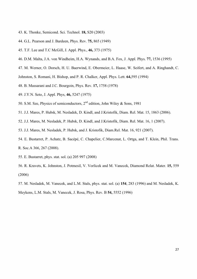
43. K. Thonke, Semicond. Sci. Technol. 18, S20 (2003)
44. G.L. Pearson and J. Bardeen, Phys. Rev. 75, 865 (1949)
45. T.F. Lee and T.C McGill, J. Appl. Phys., 46, 373 (1975)
46. D.M. Malta, J.A. von Windheim, H.A. Wynands, and B.A. Fox, J. Appl. Phys. 77, 1536 (1995)
47. M. Werner, O. Dorsch, H. U. Baerwind, E. Obermeier, L. Haase, W. Seifert, and A. Ringhandt, C.
Johnston, S. Romani, H. Bishop, and P. R. Chalker, Appl. Phys. Lett. 64,595 (1994)
48. B. Massarani and J.C. Bourgoin, Phys. Rev. 17, 1758 (1978)
49. J.Y.N. Seto, J. Appl. Phys, 46, 5247 (1975)
50. S.M. Sze, Physics of semiconductors, 2nd edition, John Wiley & Sons, 1981
51. J.J. Mares, P. Hubık, M. Nesladek, D. Kindl, and J.Kristofik, Diam. Rel. Mat. 15, 1863 (2006).
52. J.J. Mares, M. Nesladek, P. Hubık, D. Kindl, and J.Kristofik, Diam. Rel. Mat. 16, 1 (2007).
53. J.J. Mares, M. Nesladek, P. Hubık, and J. Kristofik, Diam.Rel. Mat. 16, 921 (2007).
54. E. Bustarret, P. Achatz, B. Sacépé, C. Chapelier, C.Marcenat, L. Ortga, and T. Klein, Phil. Trans.
R. Soc.A 366, 267 (2008).
55. E. Bustarret, phys. stat. sol. (a) 205 997 (2008)
56. R. Kravets, K. Johnston, J. Potmesil, V. Vorlicek and M. Vanecek, Diamond Relat. Mater. 15, 559
(2006)
57. M. Nesladek, M. Vanecek, and L.M. Stals, phys. stat. sol. (a) 154, 283 (1996) and M. Nesladek, K.
Meykens, L.M. Stals, M. Vanecek, J. Rosa, Phys. Rev. B 54, 5552 (1996)
28
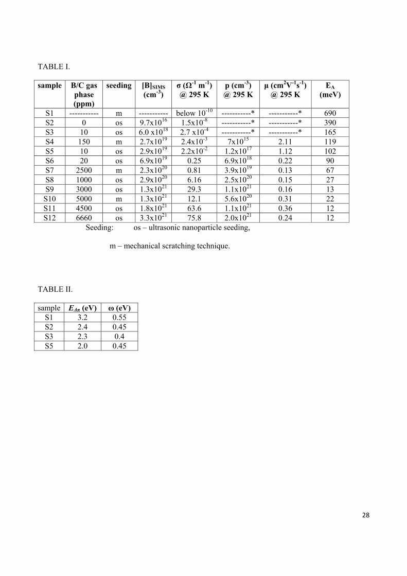
TABLE I.
sample B/C gas phase (ppm)
seeding [B]SIMS (cm-3)
σ (Ω-1 m-1) @ 295 K
p (cm-3) @ 295 K
μ (cm2V-1s-1) @ 295 K
EA (meV)
S1 ----------- m ----------- below 10-10 -----------* -----------* 690 S2 0 os 9.7x10¹⁶ 1.5x10⁻⁸ -----------* -----------* 390 S3 10 os 6.0 x10¹⁸ 2.7 x10⁻⁴ -----------* -----------* 165 S4 150 m 2.7x10¹⁹ 2.4x10⁻³ 7x10¹⁵ 2.11 119 S5 10 os 2.9x10¹⁹ 2.2x10⁻² 1.2x10¹⁷ 1.12 102 S6 20 os 6.9x10¹⁹ 0.25 6.9x10¹⁸ 0.22 90 S7 2500 m 2.3x10²⁰ 0.81 3.9x10¹⁹ 0.13 67 S8 1000 os 2.9x10²⁰ 6.16 2.5x10²⁰ 0.15 27 S9 3000 os 1.3x10²¹ 29.3 1.1x10²¹ 0.16 13
S10 5000 m 1.3x10²¹ 12.1 5.6x10²⁰ 0.31 22 S11 4500 os 1.8x10²¹ 63.6 1.1x10²¹ 0.36 12 S12 6660 os 3.3x10²¹ 75.8 2.0x10²¹ 0.24 12
Seeding: os – ultrasonic nanoparticle seeding,
m – mechanical scratching technique.
TABLE II.
sample EΔπ (eV) ω (eV) S1 3.2 0.55 S2 2.4 0.45 S3 2.3 0.4 S5 2.0 0.45
29
TABLE I. A summary of the main characteristics of NCD films. Samples S1,S2 and S3 -* did not show
the Hall effect.
TABLE II. Fitting parameters of the boron-doped NCD films absorption (Fig. 14).
30
0 50 100 150 200 250 300 3501016
1017
1018
1019
1020
1021
1022
S3
S12S9
S7S6
S5
S2
[B] S
IMS (c
m-3)
depth (nm)
FIGURE 1.
31
1000 1200 1400 1600 1800
S6
UNCD
SCD
Boron free
1021
1019
[B]SIMS
(cm-3)
S12S10
S7
S2
S1
λ=325 nm295 K D G
Inte
nsity
(arb
. uni
ts)
Wavenumber (cm-1)
FIGURE 2.
32
109 1017 1018 1019 1020 1021 10221290
1300
1310
1320
1330
S1 S2 S6 S7 S10
S12
vRaman
line
pos
ition
(cm
-1)
[B]SIMS (cm-3)
109 1017 1018 1019 1020 1021 1022
0.0
0.5
1.0
1.5
2.0
2.5
3.0xx
I diam
ond /
(I D +
I G)
FIGURE 3.
33
FIGURE 4.
34
1 2 3 4 5 6 7 8 9 1010-10
10-8
10-6
10-4
10-2
100
102
EA= 160 meV
,
1021
1016[B]SIMS
(cm-3)
S3
S2
EA= 680 meV
S1
S5S7S10S12 EA= 12 meV
ESCD,IIb= 370 meV
EA= 390 meV
EA= 120 meV
EA= 67 meV
EA= 22 meV
cond
uctiv
ity (S
cm
-1)
1000/T (K-1)
FIGURE 5.
35
1013 1015 1017 1019 10210.0
0.1
0.2
0.3
0.4
NCD films SCD, Ref. 17 SCD, Ref. 18 PCD, Ref. 19 PCD, Ref. 45 PCD, Ref. 46
Pearson-Bardeen model: α = 5.1x10⁻⁸ eV/cm α = 6.7x10⁻⁸ eV/cm
EA (e
V)
[B]SIMS (cm-3)
FIGURE 6.
36
1016 1017 1018 1019 1020 1021 102210-9
10-7
10-5
10-3
10-1
101
103
metal-insulatortransitionin SCD
(a)
metallictransport
hoppingtransport
activated valence-bandtransport
[B]SIMS (cm-3)
NCD, this work SCD, Ref. 19,20 SCD, Ref. 46 PCD, Ref. 47 Seto model Eqn. (4)
σ 300K
(Ω-1 c
m-1)
1016 1017 1018 1019 1020 1021 10221013
1014
1015
1016
1017
1018
1019
1020
1021
1022(b)
ND
Theoretical prediction ofcarrier concentration
Pearson-Bardeen p after Eqn. (3)
NCD, this work SCD, Ref. 46 PCD, Ref. 46 PCD, Ref. 47
p 300K
(cm
-3)
[B]SIMS (cm-3)
FIGURE 7.
37
300 400 500 600 700
10-1
100
(b)
S12μ ~ T -1.5
S4μ ~ T -1
1021
[B]SIMS
(cm-3)1019
S5μ ~ T -0.9
S8μ ~ T 0.5
S7μ ~ T 0.8
S9μ ~ T 2.9
mob
ility
(cm
2 V-1 s
-1)
T (K)
FIGURE 8.
1.5 2.0 2.5 3.0 3.5
1016
1017
1018
1019
1020
1021
1022(a)S11: [B]SIMS
S8: [B]SIMS
S7Ea=0.07 eV
ND=1x1018 cm-3
S6Ea=0.09 eV
ND=1x1018 cm-3
S5Ea=0.23 eV
ND=1x1018 cm-3S4Ea=0.32 eV
ND=1x1018 cm-3
p (c
m-3)
1000/T (K-1)
38
1013 1015 1017 1019 1021
10-3
10-2
10-1
100
101
102
103
104
μ ~ 1/p
NCD SCD, Ref. 46 PCD, Ref. 47 after Seto model
μ 300K
(cm
2 V-1 s
-1)
hole density (cm-3)
FIGURE 9.
39
1 10 100
10-4
10-3
10-2
10-1
100
101
102
S7 S8 S10 S11 S12
ρ/ρ 30
0K
T (K)
FIGURE 10.
40
0 50 100 150 200 250 300
0
100
200
300
400 S7 S11 S8 S12 S10
σ* = σ/σ300K
EA (T) < kBT
EA (T) > kBT
- dlnσ*
/d(1
/T)
T (K)
FIGURE 11.
41
0.50 0.75 1.00 1.25 1.50 1.75 2.00
S1, boron-free, 85K S2 n.i.d., 85K S2 n.i.d., 295K S4, 85K undoped UNCDN
orm
. pho
tocu
rren
t (ar
b.un
its)
Photon energy (eV)
FIGURE 12.
42
3.5 4.0 4.5 5.0 5.5 6.0
IIa SCD
undopedUNCD
S1
S2
295 K"as grown"
S6
Nor
m. p
hoto
curr
ent (
arb.
units
)
Photon energy (eV)
FIGURE 13.
43
1 2 3 4 5101
102
103
104
105saturation
π - π*1016
1021
[B]SIMS
(cm-3)
π - π*
undoped PCD
π - π* π - σ*Σ - Σ*
S12
S4
S2
S1
αP
DS (c
m-1)
Energy (eV)
FIGURE 14.
44
FIG. 1. Doping profiles of boron doped NCD films as measured by SIMS.
FIG. 2. Raman spectra of boron doped NCD films compared with Raman spectra of undoped SCD and
UNCD films. The main features in the spectra previously reported in NCD films34,35,36 are marked with
the dashed line. Spectra were recorded with 325 nm excitation line at ambient conditions. The spectra
are shifted vertically for clarity.
FIG. 3. Position of the diamond first order line estimated from Raman spectra and the ratio of diamond
first order line Idiamond intensity to the sum of D and G band insensitivities, ID and IG respectively, as a
function of boron concentration obtained by SIMS.
FIG. 4. AFM images of the non-intentionally doped NCD film S2 (a), intermediate boron-doped NCD
film S7 (2.3x1020 cm-3) (b) and heavily doped S10 (1.3x1021 cm-3) (c) and heavily doped NCD film S12
([B]SIMS = 3.3x1021 cm-3) (d). The measurements were performed at ambient conditions; 1x1 µm
images were recorded.
FIG. 5. Temperature dependence of the conductivity measured in NCD films. The boron concentration
change derived by SIMS experiments is marked on the right side of the graph. The activation energies
EA were calculated for the high temperature range of the conductivity dependence.
FIG. 6. Dependence of the conductivity activation energy, EA, on the boron doping in NCD films. The
activation energies were calculated for the high temperature range of the conductivity dependence (see
Fig. 4). A theoretical curve according to Eqn. 3 is given by the solid curve. Experimental data reported
for homoepitaxial diamond films20,21 and polycrystalline diamond films17,18 are plotted for comparison.
45
FIG. 7. Room temperature conductivity (a) and carrier concentration (b) as a function of boron doping
measured for NCD films. Values reported in the literature are plotted for comparison.20,21,22,46,47 The
position of the onsets for the changes from valence band conduction to hopping conduction as well as
from hopping conduction into metallic conduction as predicted by theoretical model20,42 are marked
with the dashed lines. The curve predicted by the Seto model of conductivity is plotted in (a) as a solid
line. A solid line in (b) represents the expected carrier concentration calculated using Eqn. (3) using the
activation energy obtained from temperature dependence of carrier concentration and a dashed line the
carrier concentration calculated within the Pearson-Bardeen model.44
FIG. 8. Temperature dependence of the carrier (hole) concentration (a) and carrier mobility (b)
measured in temperature range from 295K to 650K. The solid lines in (a) represent best fit according to
Eqn. (3). The fitting parameters are summarized in the graph. For heavily boron-doped NCD films
boron concentrations derived from SIMS experiments are marked by dashed lines. The lines in (b)
correspond to best fits of the temperature-dependent mobility using μ ~ Tγ, where the y parameters are
given in the graph for each NCD film.
FIG. 9. Hole mobility dependence on hole concentration in NCD films. The data for B-doped single
crystal46 and polycrystalline diamond films47 available in the literature were plotted for comparison.
The dashed line represents the expected mobility dependence µ ~ 1/p due to ionized acceptors. Dashed
line represents the mobility (Eqn. 4) curve predicted by the Seto model.
FIG. 10 Temperature dependence of the normalized resistance ρ/ ρ(300K) from 300K down to 50mK.
Highly doped samples with doping concentration above 1021 cm-3 show superconductivity with a
critical temperature of about 2K.
46
FIG. 11. Effective activation energy Eact as determined from the slope of the Arrhenius plot of the
temperature dependent conductivity normalized to its room temperature value. Only weakly doped
samples (S7) show thermally activated hopping conduction, whereas higher doped samples behave like
disordered metals.
FIG. 12. Normalized spectrally resolved photocurrent in “as grown” NCD films with different boron
concentration (boron-free, non-intentionally doped – 9.7x1016 cm-3, and low boron doped – 2.7x10¹⁹
cm-3) measured at 85K. The spectrum of non-intentionally doped NCD film S2 at 295K was plotted to
show a temperature dependence of the photocurrent signal observed as an onset at about 0.6 eV. The
spectrum of the UNCD film is presented to compare the influence of the amorphous carbon in the grain
boundaries on the photocurrent signal. The spectra were shifted vertically to emphasis the differences.
FIG. 13. Normalized spectrally resolved photocurrent in “as grown” NCD films with different boron
concentration (boron-free, non-intentionally doped – 9.7x1016 cm-3, and low boron doped – 6.9x10¹⁹
cm-3) in the high energy range. A difference in the expected band-to-band absorption onset is present
depending on the boron incorporation in the film. Shift to the lower energy is expected to originate
from the absorption in the band tails due to disorder.
FIG. 14. PDS absorption coefficient αopt calculated for NCD samples. The onset at about 0.8 eV is
attributed to transitions from the π to π* band.