Embed Size (px)
Citation preview
DATA SHEET
Product specificationSupersedes data of March 1992File under Integrated Circuits, IC11
June 1994
INTEGRATED CIRCUITS
Philips Semiconductors
TDA5145Brushless DC motor drive circuit

June 1994 2
Philips Semiconductors Product specification
Brushless DC motor drive circuit TDA5145
FEATURES
• Full-wave commutation (using push/pull drivers at theoutput stages) without position sensors
• Built-in start-up circuitry
• Three push-pull outputs:
– output current 2.0 A (typ.)
– built-in current limiter
– soft-switching outputs for low ElectromagneticInterference (EMI)
• Thermal protection
• Flyback diodes
• Tacho output without extra sensor
• Motor brake facility
• Direction control input
• Reset function
• Transconductance amplifier for an external controltransistor.
APPLICATIONS
• General purpose spindle driver e.g.:
– Hard disk drive
– Tape drive
– Optical disk drive.
GENERAL DESCRIPTION
The TDA5145 is a bipolar integrated circuit used to drive3-phase brushless DC motors in full-wave mode. Thedevice is sensorless (saving of 3 hall-sensors) using theback-EMF sensing technique to sense the rotor position.It includes bidirectional control, brake function and has aspecial circuit built-in to reduce the EMI (soft switchingoutput stages).
QUICK REFERENCE DATAMeasured over full voltage and temperature range.
Notes
1. An unstabilized supply can be used.
2. VVMOT = VP; +AMP IN = −AMP IN = 0 V; all outputs IO = 0 mA.
ORDERING INFORMATION
SYMBOL PARAMETER CONDITIONS MIN. TYP. MAX. UNIT
VP supply voltage note 1 4 − 18 V
VVMOT input voltage to the output driverstages
note 2 1.7 − 16 V
VDO drop-out output voltage IO = 100 mA − 0.90 1.05 V
ILIM current limiting VVMOT = 10 V; RO = 1.2 Ω 1.8 2.0 2.5 A
TYPE NUMBERPACKAGE
PINS PIN POSITION MATERIAL CODE
TDA5145 28 DIL plastic SOT117-1
TDA5145T 28 SOL plastic SOT136-1
June 1994 3
Philips Semiconductors Product specification
Brushless DC motor drive circuit TDA5145
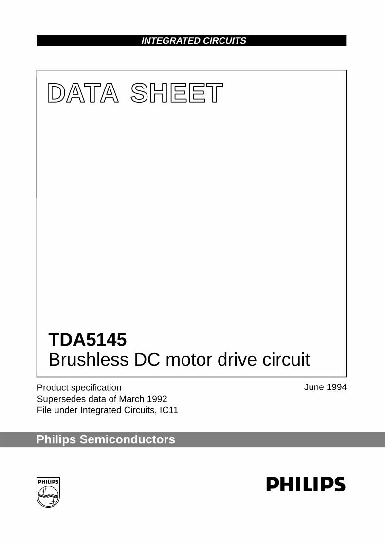
BLOCK DIAGRAM
BBBBBBBBBBBBBBBBBBBBBBBBBBBBBBBBBBBBBBBBBBBBBBBBBBBBBBBBBBBBBBBBBBBBBBBBBBBBBBBBBBBBBBBBBBBBBBBBBBBBBBBBBBBBBBBBBBBBBBBBBBBBBBBBBBBBBBBBBBBBBBBBBBBBBBBBBBBBBBBBBBBBBBBBBBBBBBBBBBBBBBBBBBBBBBBBBBBBBBBBBBBBBBBBBBBBBBBBBBBBBBBBBBBBBBBBBBBBBBBBBBBBBBBBBBBBBBBBBBBBBBBBBBBBBBBBBBBBBBBBBBBBBBBBBBBBBBBBBBBBBBBBBBBBBBBBBBBBBBBBBBBBBBBBBBBBBBBBBBBBBBBBBBBBBBBBBBBBBBBBBBBBBBBBBBBBBBBBBBBBBBBBBBBBBBBBBBBBBBBBBBBBBBBBBBBBBBBBBBBBBBBBBBBBBBBBBBBBBBBBBBBBBBBBBBBBBBBBBBBBBBBBBBBBBBBBBBBBBBBBBBBBBBBBBBBBBBBBBBBBBBBBBBBBBBBBBBBBBBBBBBBBBBBBBBBBBBBBBBBBBBBBBBBBBBBBBBBBBBBBBBBBBBBBBBBBBBBBBBBBBBBBBBBBBBBBBBBBBBBBBBBBBBBBBBBBBBBBBBBBBBBBBBBBBBBBBBBBBBBBBBBBBBBBBBBBBBBBBBBBBBBBBBBBBBBBBBBBBBBBBBBBBBBBBBBBBBBBBBBBBBBBBBBBBBBBBBBBBBBBBBBBBBBBBBBBBBBBBBBBBBBBBBBBBBBBBBBBBBBBBBBBBBBBBBBBBBBBBBBBBBBBBBBBBBBBBBBBBBBBBBBBBBBBBBBBBBBBBBBBBBBBBBBBBBBBBBBBBBBBBBBBBBBBBBBBBBBBBBBBBBBBBBBBBBBBBBBBBBBBBBBBBBBBBBBBBBBBBBBBBBBBBBBBBBBBBBBBBBBBBBBB
BBBBBBBBBBBBBBBBBBBBBBBBBBBBBBBBBBBBBBBBBBBBBBBBBBBBBBBBBBBBBBBBBBBBBBBB
BBBBBBBBBBBBBBBBBBBBBBBBBBBBBBBBBBBBBBBBBBBBBBBBBBBBBBBBBBBBBBBBBBBBBBBBBBBBBBBBBBBBBBBBBBBBBBBBBBBBBBBB
BBBBBBBBBBBBBBBBBBBBBBBBBBBBBBBBBBBB
BBBBBBBBBBBBBBBBBBBBBBBBBBBBBBBBBBBBBBBBBBBBBBBBBBBBBBBBBBBBBBBBBBBBBBBBBBBBBB
BBBBBBBBBBBBBBBBBBBBBBBBBBBBBBBBBBBBBBBBBBBBBBBBBBBBBBBBBBBBBBBBBBBBBBBBBBBBBBBBBBBBBBBBBBBBBBBBBBBBBBBBBBBBBBBBBBBBBBBBBBBBBBBBBBBBBBBBBBBBBBBBBBBBBBBBBBBBBBBBBBBBBBBBBBBBBBBBBBBBBBBBBBBBBBBBBBBBBBBBBBBBBBBBBBBBBBBBBBBBBBBBBBBBBBBBBBBBBBBBBBBBBBBBBBBBBBBBBBBBBBBBBBBBBBBBBBBBBBBBBBBBBBBBBBBBBBBBBBBBBBBBBBBBBBBBBBBBBBBB
BBBBBBBBBBBBBBBBBBBBBBBBBBBBBBBBBBBBBBBBBBBBBBBBBBBBBBBBBBBBBBBBBBBBBBBBBBBBBBBBBBBBBBBBBBBBBBBBBBBBBBBBBBBBBBBBBBBBBBBBBBBBBBBBBBBBBBBBBBBBBBBBBBBBBBBBBBBBBBBBBBBBBBBBBBBBBBBBBBBBBBBBBBBBBBBBBBBBBBBBBBBBBBBBBBBBBBBBBBBBBBBBBBBBBBBBBBBBBBBBBBBBBBBBBBBBBBBBBBBBBBBBBBBBBBBBBBBBBBBBBBBBBBBBBBBBBBBBBBBBBBBBBBBBBBBBBBBBBBBBBBBBBBBBBBBBBBBBBBBBBBBBBBBBBBBBBBBBBBBBBBBBBBBBBBBBBBBBBBBBBBBBBBBBBBBBBBBBBBBBBBBBBBBBBBBBBBBBBBBBBBBBBBBBBBBBBBBBBBBBBBBBBBBBBBBBBBBBBBBBBBBBBBBBBBBBBBBBBBBBBBBBBBBBBBBBBBBBBBBBBBBBBBBBBBBBBBBBBBBBBBBBBBBBBBBBBBBBBBBB
BBBBBBBBBBBBBBBBBBBBBBBBBBBBBBBBBBBBBBBBBBBBB
BBBBBBBBBBBBBBBBBBBBBBBBBBBBBBBBBBBBBBBBBBBBBBBBBBBBBBBBBBBBBBBBBBBBBBBBBBBBBBBBBBBBBBBBBBBBBBBBBBBBBBBBBBBBBBBBBBBBBBBBBBBBBBBBBBBBBBBBBBBBBBBBBBBBBBBBBBBBBBBBB
BBBBBBBBBBBBBBBBBBBBBBBBBBBBBBBBBBBBBBBBBBBBBBBBBBBBBBBBBBBBBBBBBBBBBBBBBBBBBBBBBBBBBBBBBBBBBBBBBBBBBBBBBBBBBBBBBBBBBBBBBBBBBBBBBBBBBBBBBBBBBBBBBBBBBBBBBBBBBBBBBBBBBBBBBBBBBBBBBBBBBBBB
BBBBBBBBBBBBBBBBBBBBBBBBBBBBBBBBBBBBBBBBBBBBBBBBBBBBBBBBBBBBBBBBBBBBBBBBBBBBBBBBBBBBBBBBBBBBBBBBBBBBBBBBBBBBBBBBBBBBBBBBBBBBBBBBBBBBBBBBBBBBBBBBBBBBBBBBBBBBBBBBBBBBBBBBBBBBBBBBBBBBBBBBBBBBBBBBBBBBBBBBBBBBBBBBBBBBBBBBBBBBBBBBBBBBBBBBBBBBBBBBBBBBBBBBBBBBBBBBBBBBBBBBBBBBBBBBBBBBBBBBBBBBBBBBBBBBBBBBBBBBBBBBBBBBBBBBBBBBBBBBBBBBBBBBBBBBBBBBBBBBBBBBBBBBBBBBBBBBBBBBBBBBBBBBBBBBBBBBBBBBBBBBBBBBBBBBBBBBBBBBBBBBBBBBBBBBBBBBBBBBBBBBBBBBBBBBBBBBBBBBBBBBBBBBBBBBBBBBBBBBBBBBBBBBBBBBBBBBBBBBBBBBBBBBBBBBBBBBBBBBBBBBBBBBBBBBBBBBBBBBBBBBBBBBBBBBBBBBBBBBBBBBBBBBBBBBBBBBBBBBBBBBBBBBBBBBBBBBBBBBBBBBBBBBBBBBBBBBBBBBBBBBBBBBBBBBBBBBBBBBB
Fig.1 Block diagram.
Pin numbers for both DIL and SOL packages are identical.
June 1994 4
Philips Semiconductors Product specification
Brushless DC motor drive circuit TDA5145
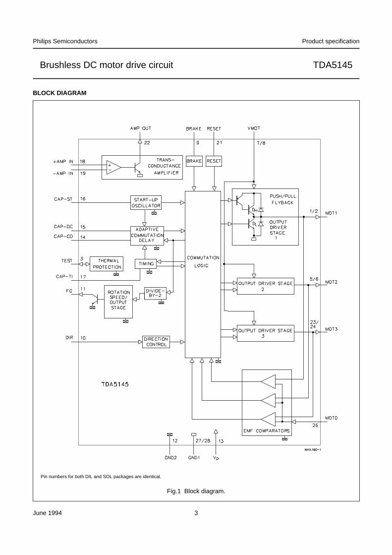
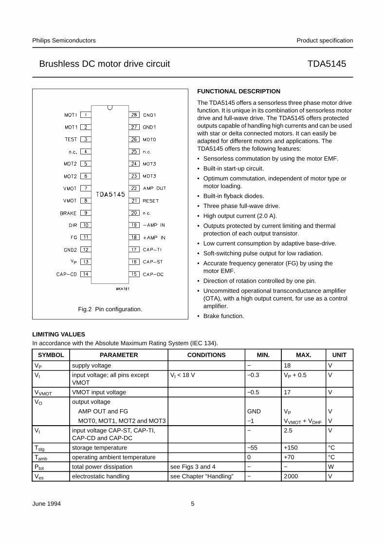
PINNING
Note
1. Pin numbers for both DIL and SOL packages are identical.
SYMBOL PIN(1) DESCRIPTION
MOT1 1 and 2 driver output 1
TEST 3 test input/output
n.c. 4 not connected
MOT2 5 and 6 driver output 2
VMOT 7 and 8 input voltage for the output driver stages
BRAKE 9 brake input; this pin may not be left floating, a LOW level voltage must be applied to disablethis function
DIR 10 direction control input; this pin may not be left floating
FG 11 frequency generator: output of the rotation speed (open collector digital output)
GND2 12 ground supply return for control circuits
VP 13 supply voltage
CAP-CD 14 external capacitor connection for adaptive communication delay timing
CAP-DC 15 external capacitor connection for adaptive communication delay timing copy
CAP-ST 16 external capacitor connection for start-up oscillator
CAP-TI 17 external capacitor connection for timing
+AMP IN 18 non-inverting input of the transconductance amplifier
−AMP IN 19 inverting input of the transconductance amplifier
n.c. 20 not connected
RESET 21 reset input; this pin may not be left floating, a LOW level voltage must be applied to disablethis function
AMP OUT 22 transconductance amplifier output (open collector)
MOT3 23 and 24 driver output 3
n.c. 25 not connected
MOT0 26 input from the star point of the motor coils
GND1 27 and 28 ground (0 V) motor supply return for output stages
June 1994 5
Philips Semiconductors Product specification
Brushless DC motor drive circuit TDA5145
Fig.2 Pin configuration.
FUNCTIONAL DESCRIPTION
The TDA5145 offers a sensorless three phase motor drivefunction. It is unique in its combination of sensorless motordrive and full-wave drive. The TDA5145 offers protectedoutputs capable of handling high currents and can be usedwith star or delta connected motors. It can easily beadapted for different motors and applications. TheTDA5145 offers the following features:
• Sensorless commutation by using the motor EMF.
• Built-in start-up circuit.
• Optimum commutation, independent of motor type ormotor loading.
• Built-in flyback diodes.
• Three phase full-wave drive.
• High output current (2.0 A).
• Outputs protected by current limiting and thermalprotection of each output transistor.
• Low current consumption by adaptive base-drive.
• Soft-switching pulse output for low radiation.
• Accurate frequency generator (FG) by using themotor EMF.
• Direction of rotation controlled by one pin.
• Uncommitted operational transconductance amplifier(OTA), with a high output current, for use as a controlamplifier.
• Brake function.
LIMITING VALUESIn accordance with the Absolute Maximum Rating System (IEC 134).
SYMBOL PARAMETER CONDITIONS MIN. MAX. UNIT
VP supply voltage − 18 V
VI input voltage; all pins exceptVMOT
VI < 18 V −0.3 VP + 0.5 V
VVMOT VMOT input voltage −0.5 17 V
VO output voltage
AMP OUT and FG GND VP V
MOT0, MOT1, MOT2 and MOT3 −1 VVMOT + VDHF V
VI input voltage CAP-ST, CAP-TI,CAP-CD and CAP-DC
− 2.5 V
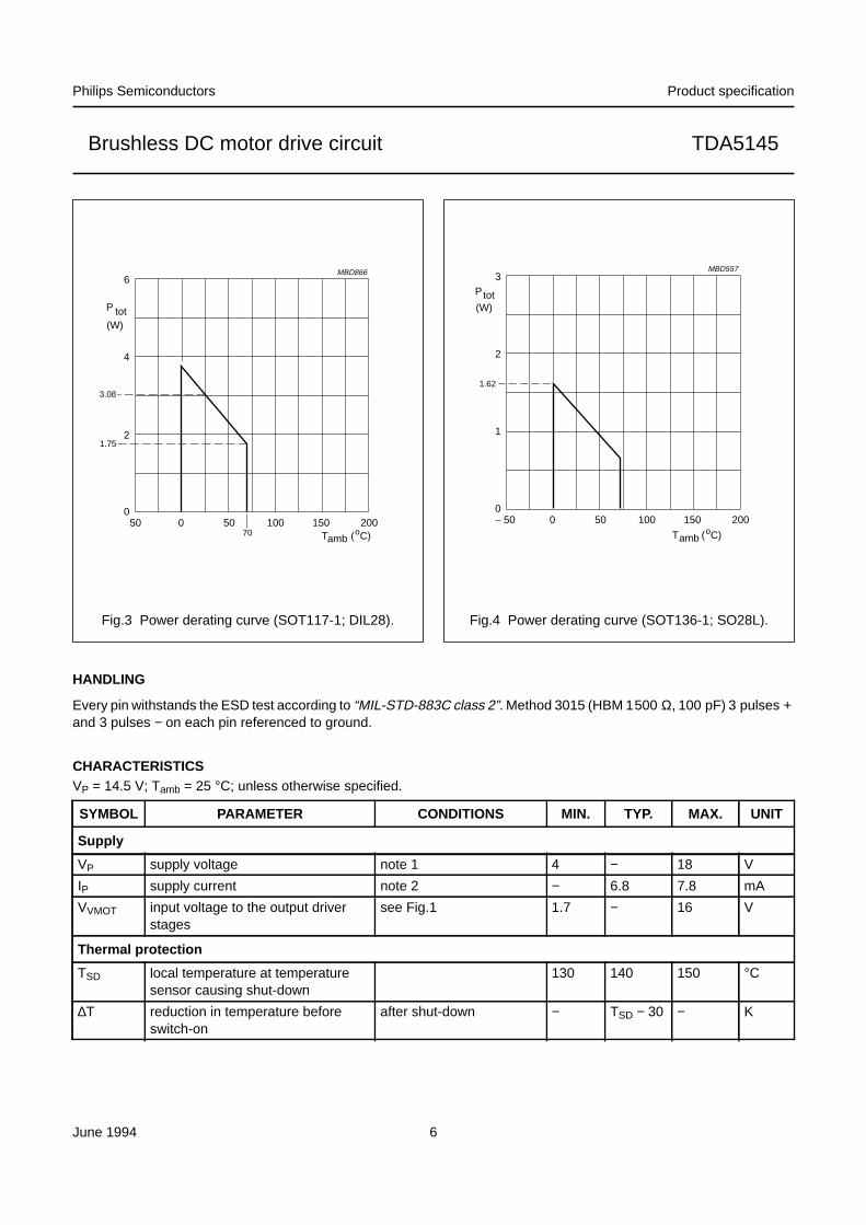
Tstg storage temperature −55 +150 °CTamb operating ambient temperature 0 +70 °CPtot total power dissipation see Figs 3 and 4 − − W
Ves electrostatic handling see Chapter “Handling” − 2000 V
June 1994 6
Philips Semiconductors Product specification
Brushless DC motor drive circuit TDA5145
handbook, halfpage
50
6
4
2
00 200
MBD866
50 100 150
P tot(W)
T ( C)ambo
3.08
1.75
70
Fig.3 Power derating curve (SOT117-1; DIL28).
Ptot(W)
50
3
2
00 200
MBD557
50 100 150
T ( C)ambo
1.62
1
Fig.4 Power derating curve (SOT136-1; SO28L).
HANDLING
Every pin withstands the ESD test according to “MIL-STD-883C class 2”. Method 3015 (HBM 1500 Ω, 100 pF) 3 pulses +and 3 pulses − on each pin referenced to ground.
CHARACTERISTICSVP = 14.5 V; Tamb = 25 °C; unless otherwise specified.
SYMBOL PARAMETER CONDITIONS MIN. TYP. MAX. UNIT
Supply
VP supply voltage note 1 4 − 18 V
IP supply current note 2 − 6.8 7.8 mA
VVMOT input voltage to the output driverstages
see Fig.1 1.7 − 16 V
Thermal protection
TSD local temperature at temperaturesensor causing shut-down
130 140 150 °C
∆T reduction in temperature beforeswitch-on
after shut-down − TSD − 30 − K
June 1994 7
Philips Semiconductors Product specification
Brushless DC motor drive circuit TDA5145
MOT0; centre tap
VI input voltage −0.5 − VVMOT V
II input bias current 0.5 V < VI < VVMOT − 1.5 V −10 − − µA
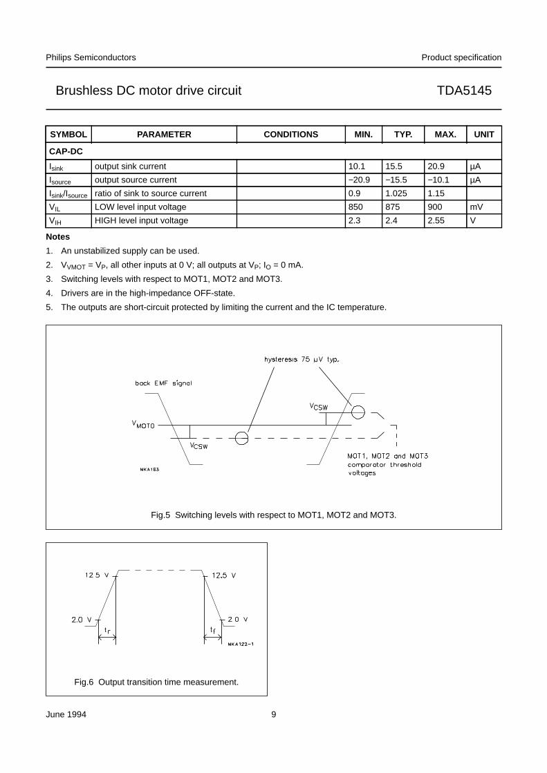
VCSW comparator switching level note 3 ±20 ±25 ±30 mV
∆VCSW variation in comparator switchinglevels
− − 3 mV
Vhys comparator input hysteresis − 75 − µV
MOT1, MOT2 and MOT3; see Fig.5
VDO drop-out output voltage IO = 100 mA − 0.9 1.05 V
IO = 1000 mA − 1.6 1.85 V
∆VOL variation in saturation voltagebetween lower transistors
IO = 100 mA − − 180 mV
∆VOH variation in saturation voltagebetween upper transistors
IO = −100 mA − − 180 mV
ILIM current limiting VVMOT = 10 V; RO = 1.2 Ω 1.8 2.0 2.5 A
tr rise time switching output VVMOT = 15 V; see Fig.6 5 10 15 µs
tf fall time switching output VVMOT = 15 V; see Fig.6 10 15 20 µs
VDHF diode forward voltage (diode DH) IO = −500 mA;notes 4 and 5; see Fig.1
− − 1.5 V
VDLF diode forward voltage (diode DL) IO = 500 mA;notes 4 and 5; see Fig.1
−1.5 − − V
IDM peak diode current note 5 − − 2.5 A
+AMP IN and −AMP IN
VI input voltage −0.3 − VP − 1.7 V
differential mode voltage without‘latch-up’
− − ±VP V
Ib input bias current − − 650 nA
CI input capacitance − 4 − pF
Voffset input offset voltage − − 10 mV
AMP OUT (open collector)
Isink output sink current 40 − − mA
Vsat saturation voltage II = 40 mA − 1.5 2.1 V
VO output voltage −0.5 − +18 V
SR slew rate RL = 330 Ω; CL = 50 pF − 60 − mA/µs
Gtr transfer gain 0.3 − − S
DIR
VIH HIGH level input voltage 4 V < VP < 18 V 2.0 − − V
VIL LOW level input voltage 4 V < VP < 18 V − − 0.8 V
IIL LOW level input current − −20 − µA
IIH HIGH level input current − 20 − µA
SYMBOL PARAMETER CONDITIONS MIN. TYP. MAX. UNIT
June 1994 8
Philips Semiconductors Product specification
Brushless DC motor drive circuit TDA5145
RESET
VIH HIGH level input voltage reset mode;4 V < VP < 18 V
2.0 − − V
VIL LOW level input voltage normal mode;4 V < VP < 18 V
− − 0.8 V
IIL LOW level input current VI = 2.0 V − −20 − µA
IIH HIGH level input current VI = 0.8 V − 20 − µA
BRAKE
VIH HIGH level input voltage brake mode;4 V < VP < 18 V
2.0 − − V
VIL LOW level input voltage normal mode;4 V < VP < 18 V
− − 0.8 V
IIL LOW level input current VI = 2.0 V − −20 − µA
IIH HIGH level input current VI = 0.8 V − 20 − µA
FG (open collector)
VOL LOW level output voltage IO = 1.6 mA − − 0.4 V
VOH(max) maximum HIGH level output voltage VP − − V
tTHL HIGH-to-LOW transition time CL = 50 pF; RL = 10 kΩ − 0.5 − µs
ratio of FG frequency andcommutation frequency
− 1 : 2 −
δ duty factor − 50 − %
CAP-ST
Isink output sink current 1.5 2.0 2.5 µA
Isource output source current −2.5 −2.0 −1.5 µA
VSWL LOW level switching voltage − 0.20 − V
VSWH HIGH level switching voltage − 2.20 − V
CAP-TI
Isink output sink current − 28 − µA
Isource output source current 0.2 V < VCAP-TI < 0.3 V − −57 − µA
0.3 V < VCAP-TI < 2.2 V − −5 − µA
VSWL LOW level switching voltage − 50 − mV
VSWM MIDDLE level switching voltage − 0.30 − V
VSWH HIGH level switching voltage − 2.20 − V
CAP-CD
Isink output sink current 10.6 16.2 22 µA
Isource output source current −5.3 −8.1 −11 µA
Isink/Isource ratio of sink to source current 1.85 2.05 2.25
VIL LOW level input voltage 850 875 900 mV
VIH HIGH level input voltage 2.3 2.4 2.55 V
SYMBOL PARAMETER CONDITIONS MIN. TYP. MAX. UNIT
June 1994 9
Philips Semiconductors Product specification
Brushless DC motor drive circuit TDA5145
Notes
1. An unstabilized supply can be used.
2. VVMOT = VP, all other inputs at 0 V; all outputs at VP; IO = 0 mA.
3. Switching levels with respect to MOT1, MOT2 and MOT3.
4. Drivers are in the high-impedance OFF-state.
5. The outputs are short-circuit protected by limiting the current and the IC temperature.
CAP-DC
Isink output sink current 10.1 15.5 20.9 µA
Isource output source current −20.9 −15.5 −10.1 µA
Isink/Isource ratio of sink to source current 0.9 1.025 1.15
VIL LOW level input voltage 850 875 900 mV
VIH HIGH level input voltage 2.3 2.4 2.55 V
SYMBOL PARAMETER CONDITIONS MIN. TYP. MAX. UNIT
Fig.5 Switching levels with respect to MOT1, MOT2 and MOT3.
Fig.6 Output transition time measurement.
June 1994 10
Philips Semiconductors Product specification
Brushless DC motor drive circuit TDA5145
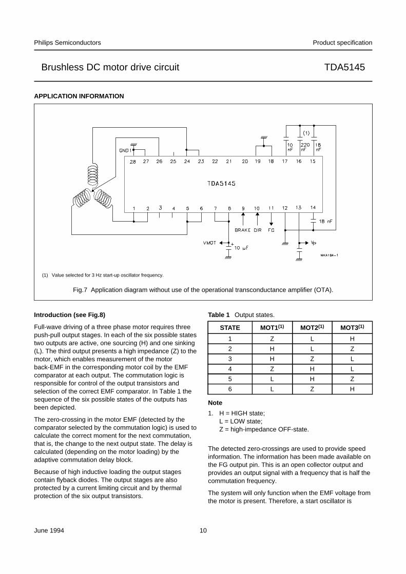
APPLICATION INFORMATION
(1) Value selected for 3 Hz start-up oscillator frequency.
Fig.7 Application diagram without use of the operational transconductance amplifier (OTA).
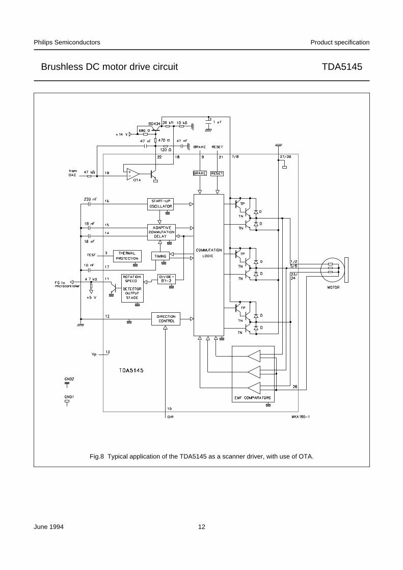
Introduction (see Fig.8)
Full-wave driving of a three phase motor requires threepush-pull output stages. In each of the six possible statestwo outputs are active, one sourcing (H) and one sinking(L). The third output presents a high impedance (Z) to themotor, which enables measurement of the motorback-EMF in the corresponding motor coil by the EMFcomparator at each output. The commutation logic isresponsible for control of the output transistors andselection of the correct EMF comparator. In Table 1 thesequence of the six possible states of the outputs hasbeen depicted.
The zero-crossing in the motor EMF (detected by thecomparator selected by the commutation logic) is used tocalculate the correct moment for the next commutation,that is, the change to the next output state. The delay iscalculated (depending on the motor loading) by theadaptive commutation delay block.
Because of high inductive loading the output stagescontain flyback diodes. The output stages are alsoprotected by a current limiting circuit and by thermalprotection of the six output transistors.
Table 1 Output states.
Note
1. H = HIGH state;L = LOW state;Z = high-impedance OFF-state.
The detected zero-crossings are used to provide speedinformation. The information has been made available onthe FG output pin. This is an open collector output andprovides an output signal with a frequency that is half thecommutation frequency.
The system will only function when the EMF voltage fromthe motor is present. Therefore, a start oscillator is
STATE MOT1(1) MOT2(1) MOT3(1)
1 Z L H
2 H L Z
3 H Z L
4 Z H L
5 L H Z
6 L Z H
June 1994 11
Philips Semiconductors Product specification
Brushless DC motor drive circuit TDA5145
provided that will generate commutation pulses when nozero-crossings in the motor voltage are available.
A timing function is incorporated into the device for internaltiming and for timing of the reverse rotation detection.
The TDA5145 also contains an uncommittedtransconductance amplifier (OTA) that can be used as acontrol amplifier. The output is capable of directly drivingan external power transistor.
The TDA5145 is designed for systems with low currentconsumption: use of I2L logic, adaptive base drive for theoutput transistors (patented).
Adjustments
The system has been designed in such a way that thetolerances of the application components are not critical.However, the approximate values of the followingcomponents must still be determined:
• The start capacitor; this determines the frequency of thestart oscillator.
• The two capacitors in the adaptive commutation delaycircuit; these are important in determining the optimummoment for commutation, depending on the type andloading of the motor.
• The timing capacitor; this provides the system with itstiming signals.
THE START CAPACITOR (CAP-ST)
This capacitor determines the frequency of the startoscillator. It is charged and discharged, with a current of2 µA, from 0.05 to 2.2 V and back to 0.05 V. The timetaken to complete one cycle is given by:tstart = (2.15 × C) s (with C in µF)
The start oscillator is reset by a commutation pulse and sois only active when the system is in the start-up mode. Apulse from the start oscillator will cause the outputs tochange to the next state (torque in the motor). If themovement of the motor generates enough EMF theTDA5145 will run the motor. If the amount of EMFgenerated is insufficient, then the motor will move one steponly and will oscillate in its new position. The amplitude ofthe oscillation must decrease sufficiently before the arrivalof the next start pulse, to prevent the pulse arriving duringthe wrong phase of the oscillation. The oscillation of themotor is given by:
where:
Kt = torque constant (N.m/A)
I = current (A)
p = number of magnetic pole-pairs
J = inertia J (kg.m2)
Example: J = 72 × 10−6 kg.m2, K = 25 × 10−3 N.m/A, p = 6and I = 0.5 A; this gives fosc = 5 Hz. If the damping is highthen a start frequency of 2 Hz can be chosen ort = 500 ms, thus C = 0.5/2 = 0.25 µF (choose 220 nF).
THE ADAPTIVE COMMUTATION DELAY (CAP-CD AND
CAP-DC)
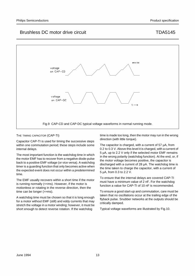
In this circuit capacitor CAP-CD is charged during onecommutation period, with an interruption of the chargingcurrent during the diode pulse. During the nextcommutation period this capacitor (CAP-CD) is dischargedat twice the charging current. The charging current is8.1 µA and the discharging current 16.2 µA; the voltagerange is from 0.9 to 2.2 V. The voltage must stay withinthis range at the lowest commutation frequency ofinterest, fC1:
(C in nF)
If the frequency is lower, then a constant commutationdelay after the zero-crossing is generated by the dischargefrom 2.2 to 0.9 V at 16.2 µA;maximum delay = (0.076 × C) ms (with C in nF)
Example: nominal commutation frequency = 900 Hz andthe lowest usable frequency = 400 Hz; so:
(choose 18 nF)
The other capacitor, CAP-DC, is used to repeat the samedelay by charging and discharging with 15.5 µA. The samevalue can be chosen as for CAP-CD. Figure 9 illustratestypical voltage waveforms.
fosc1
2πKt I× p×
J-----------------------
-----------------------------------=
C 8.1 106–×
f 1.3×--------------------------6231fC1
-------------= =
CAP-CD 6231400
------------- 15.6= =
June 1994 12
Philips Semiconductors Product specification
Brushless DC motor drive circuit TDA5145
Fig.8 Typical application of the TDA5145 as a scanner driver, with use of OTA.
BBBBBBBBBBBBBBBBBBBBBBBBBBBBBBBBBBBBBBBBBBBBBBBBBBBBBBBBBBBBBBBBBBBBBBBBBBBBBBBBBBBBBBBBBBBBBBBBBBBBBBBBBBBBBBBBBBBBBBBBBBBBBBBBBBBBBBBBBBBBBBBBBBBBBBBBBBBBBBBBBBBBBBBBBBBBBBBBBBBBBBBBBBBBBBBBBBBBBBBBBBBBBBBBBBBBBBBBBBBBBBBBBBBBBBBBBBBBBBBBBBBBBBBBBBBBBBBBBBBBBBBBBBBBBBBBBBBBBBBBBBBBBBBBBBBBBBBBBBBBBBBBBBBBBBBBBBBBBBBBBBBBBBBBBBBBBBBBBBBBBBBBBBBBBBBBBBBBBBBBBBBBBBBBBBBBBBBBBBBBBBBBBBBBBBBBBBBBBBBBBBBBBBBBBBBBBBBBBBBBBBBBBBBBBBBBBBBBBBBBBBBBBBBBBBBBBBBBBBBBBBBBBBBBBBBBBBBBBBBBBBBBBBBBBBBBBBBBBBBBBBBBBBBBBBBBBBBBBBBBBBBBBBBBBBBBBBBBBBBBBBBBBBBBBBBBBBBBBBBBBBBBBBBBBBBBBBBBBBBBBBBBBBBBBBBBBBBBBBBBBBBBBBBBBBBBBBBBBBBBBBBBBBBBBBBBBBBBBBBBBBBBBBBB
BBBBBBBBBBBBBBBBBBBBBBBBBBBBBBBBBBBBBBBBBBBBBBBBBB
BBBBBBBBBBBBBBBBBBBBBBBBBBBBBBBBBBBBBBBBBBBBBBBBBBBBBBBBBBBB
BBBBBBBBBBBBBBBBBBBBB
BBBBBBBBBBBBBBBBBBBBBBBBBBBBBBBBBBBBBBBBBBBBBBBBBB
BBBBBBBBBBBBBBBBBBBBBBBBBBBBBBBBBBBBBBBBBBBBBBBBBBBBBBBBBBBBBBBBBBBBBBBBBBBBBBBBBBBBBBBB
BBBBBBBBBBBBBBBBBBBBBBBBBBBBBBBBBBBBBBBBBBBBBBBBBBBBBBBBBBBBBBBBBBBBBBBBBBBBBBBBBBBBBBBBBBBBBBBBBBBBBBBBBBBBBBBBBBBBBBBBBBBBBBBBBBBBBBBBBBBBBBBBBBBBBBBBBBBBBBBBBBBBBBBBBBBBBBBBBBBBBBBBBBBBBBBBBBBBBBBBBBBBBBBBBBBBBBBBBBBBBBBBBBBBBBBBBBBBBBBBBBBBBBBBBBBBBBBBBBBBBBBBBBBBBBBBBBBBBBBBBBBBBBBBBBBBBBBBBBBBBBBBBBBBBBBBBBBBBBBBBBBBBBBBBBBBBBBBBBBBBBBBBBBBBBBBBBBBBBBBBBBBBBBBBBBBBBBBBBBBBBBBBBBBBBB
BBBBBBBBBBBBBBBBBBBBBBBB
June 1994 13
Philips Semiconductors Product specification
Brushless DC motor drive circuit TDA5145
Fig.9 CAP-CD and CAP-DC typical voltage waveforms in normal running mode.
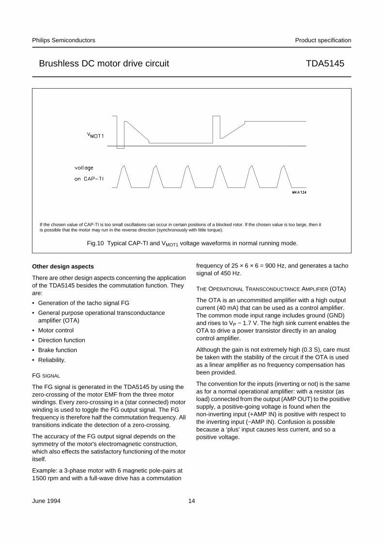
THE TIMING CAPACITOR (CAP-TI)
Capacitor CAP-TI is used for timing the successive stepswithin one commutation period; these steps include someinternal delays.
The most important function is the watchdog time in whichthe motor EMF has to recover from a negative diode-pulseback to a positive EMF voltage (or vice versa). A watchdogtimer is a guarding function that only becomes active whenthe expected event does not occur within a predeterminedtime.
The EMF usually recovers within a short time if the motoris running normally (<<ms). However, if the motor ismotionless or rotating in the reverse direction, then thetime can be longer (>>ms).
A watchdog time must be chosen so that it is long enoughfor a motor without EMF (still) and eddy currents that maystretch the voltage in a motor winding; however, it must beshort enough to detect reverse rotation. If the watchdog
time is made too long, then the motor may run in the wrongdirection (with little torque).
The capacitor is charged, with a current of 57 µA, from0.2 to 0.3 V. Above this level it is charged, with a current of5 µA, up to 2.2 V only if the selected motor EMF remainsin the wrong polarity (watchdog function). At the end, or, ifthe motor voltage becomes positive, the capacitor isdischarged with a current of 28 µA. The watchdog time isthe time taken to charge the capacitor, with a current of5 µA, from 0.3 to 2.2 V.
To ensure that the internal delays are covered CAP-TImust have a minimum value of 2 nF. For the watchdogfunction a value for CAP-TI of 10 nF is recommended.
To ensure a good start-up and commutation, care must betaken that no oscillations occur at the trailing edge of theflyback pulse. Snubber networks at the outputs should becritically damped.
Typical voltage waveforms are illustrated by Fig.10.
June 1994 14
Philips Semiconductors Product specification
Brushless DC motor drive circuit TDA5145
Fig.10 Typical CAP-TI and VMOT1 voltage waveforms in normal running mode.
If the chosen value of CAP-TI is too small oscillations can occur in certain positions of a blocked rotor. If the chosen value is too large, then itis possible that the motor may run in the reverse direction (synchronously with little torque).
Other design aspects
There are other design aspects concerning the applicationof the TDA5145 besides the commutation function. Theyare:
• Generation of the tacho signal FG
• General purpose operational transconductanceamplifier (OTA)
• Motor control
• Direction function
• Brake function
• Reliability.
FG SIGNAL
The FG signal is generated in the TDA5145 by using thezero-crossing of the motor EMF from the three motorwindings. Every zero-crossing in a (star connected) motorwinding is used to toggle the FG output signal. The FGfrequency is therefore half the commutation frequency. Alltransitions indicate the detection of a zero-crossing.
The accuracy of the FG output signal depends on thesymmetry of the motor's electromagnetic construction,which also effects the satisfactory functioning of the motoritself.
Example: a 3-phase motor with 6 magnetic pole-pairs at1500 rpm and with a full-wave drive has a commutation
frequency of 25 × 6 × 6 = 900 Hz, and generates a tachosignal of 450 Hz.
THE OPERATIONAL TRANSCONDUCTANCE AMPLIFIER (OTA)
The OTA is an uncommitted amplifier with a high outputcurrent (40 mA) that can be used as a control amplifier.The common mode input range includes ground (GND)and rises to VP − 1.7 V. The high sink current enables theOTA to drive a power transistor directly in an analogcontrol amplifier.
Although the gain is not extremely high (0.3 S), care mustbe taken with the stability of the circuit if the OTA is usedas a linear amplifier as no frequency compensation hasbeen provided.
The convention for the inputs (inverting or not) is the sameas for a normal operational amplifier: with a resistor (asload) connected from the output (AMP OUT) to the positivesupply, a positive-going voltage is found when thenon-inverting input (+AMP IN) is positive with respect tothe inverting input (−AMP IN). Confusion is possiblebecause a ‘plus’ input causes less current, and so apositive voltage.

June 1994 15
Philips Semiconductors Product specification
Brushless DC motor drive circuit TDA5145
MOTOR CONTROL
DC motors can be controlled in an analog manner usingthe OTA.
For the analog control an external transistor is required.The OTA can supply the base current for this transistorand act as a control amplifier (see Fig.8).
DIRECTION FUNCTION
If the voltage at pin 10 is <0.8 V, the motor is running inone direction (depending on the motor connections). If thevoltage at pin 10 >2.0 V, the motor is running in the otherdirection.
BRAKE FUNCTION
If the voltage at pin 9 is >2.0 V, the motor brakes. In thatcondition, the 3 outputs MOT1, MOT2 and MOT3 are
forced at a LOW voltage level and the current limitation isdone internally by the sink drivers.
RESET FUNCTION
If the voltage at pin 21 is >2.0 V, the output states areshown in Table 2.
Table 2 Output states if VRESET > 2.0 V.
Note
1. Z = high-impedance OFF-state; L = LOW state;H = HIGH state.
DRIVER OUTPUT STATE(1)
MOT1 Z
MOT2 L
MOT3 H
Table 3 Switching sequence after a reset pulse.
Note
1. Z = high-impedance OFF-state; L = LOW state; H = HIGH state.
DIR(1) RESET(1) MOT1(1) MOT2(1) DIR(1) FUNCTION
H H Z L H reset
H L Z L H normal direction modesequenceH L H L Z
H L H Z L
H L Z H L
H L L H Z
H L L Z H
L H H L Z reset
L L H L Z reverse direction modesequenceL L Z L H
L L L Z H
L L L H Z
L L Z H L
L L H Z L
June 1994 16
Philips Semiconductors Product specification
Brushless DC motor drive circuit TDA5145
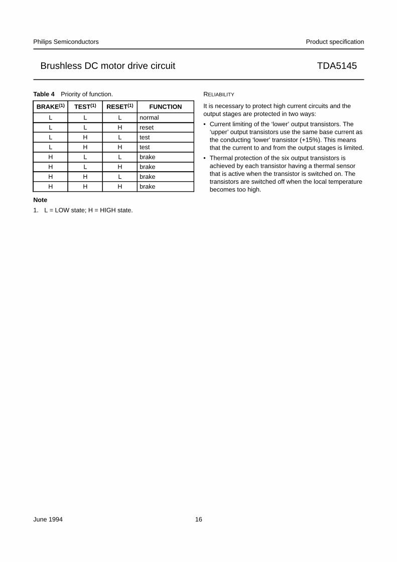
Table 4 Priority of function.
Note
1. L = LOW state; H = HIGH state.
BRAKE (1) TEST(1) RESET(1) FUNCTION
L L L normal
L L H reset
L H L test
L H H test
H L L brake
H L H brake
H H L brake
H H H brake
RELIABILITY
It is necessary to protect high current circuits and theoutput stages are protected in two ways:
• Current limiting of the ‘lower’ output transistors. The‘upper’ output transistors use the same base current asthe conducting ‘lower’ transistor (+15%). This meansthat the current to and from the output stages is limited.
• Thermal protection of the six output transistors isachieved by each transistor having a thermal sensorthat is active when the transistor is switched on. Thetransistors are switched off when the local temperaturebecomes too high.
June 1994 17
Philips Semiconductors Product specification
Brushless DC motor drive circuit TDA5145
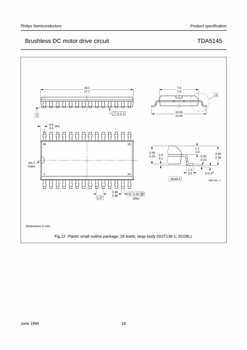
PACKAGE OUTLINES
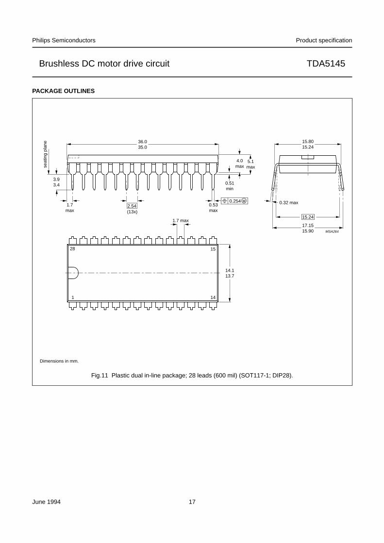
Fig.11 Plastic dual in-line package; 28 leads (600 mil) (SOT117-1; DIP28).
Dimensions in mm.
handbook, full pagewidth
28
1
15
14
1.7 max
14.113.7
36.035.0
4.0max
5.1max
0.51min
3.93.4
seat
ing
plan
e
0.254 M0.53max
2.54(13x)
1.7max
15.8015.24
0.32 max
15.24
17.1515.90 MSA264
June 1994 18
Philips Semiconductors Product specification
Brushless DC motor drive circuit TDA5145
handbook, full pagewidth7.67.4
10.6510.00
A
MBC236 - 1
0.30.1
2.452.25
1.10.5
0.320.23
1.11.0
0 to 8o
2.652.35
detail A
S
18.117.7
0.1 S
1 14
1528
pin 1index
0.90.4
(4x)
0.25 M
(28x)
0.490.36
1.27
Fig.12 Plastic small outline package; 28 leads; large body (SOT136-1; SO28L).
Dimensions in mm.
June 1994 19
Philips Semiconductors Product specification
Brushless DC motor drive circuit TDA5145
SOLDERING
Plastic small-outline packages
BY WAVE
During placement and before soldering, the componentmust be fixed with a droplet of adhesive. After curing theadhesive, the component can be soldered. The adhesivecan be applied by screen printing, pin transfer or syringedispensing.
Maximum permissible solder temperature is 260 °C, andmaximum duration of package immersion in solder bath is10 s, if allowed to cool to less than 150 °C within 6 s.Typical dwell time is 4 s at 250 °C.
A modified wave soldering technique is recommendedusing two solder waves (dual-wave), in which a turbulentwave with high upward pressure is followed by a smoothlaminar wave. Using a mildly-activated flux eliminates theneed for removal of corrosive residues in mostapplications.
BY SOLDER PASTE REFLOW
Reflow soldering requires the solder paste (a suspensionof fine solder particles, flux and binding agent) to beapplied to the substrate by screen printing, stencilling orpressure-syringe dispensing before device placement.
Several techniques exist for reflowing; for example,thermal conduction by heated belt, infrared, andvapour-phase reflow. Dwell times vary between 50 and300 s according to method. Typical reflow temperaturesrange from 215 to 250 °C.
Preheating is necessary to dry the paste and evaporatethe binding agent. Preheating duration: 45 min at 45 °C.
REPAIRING SOLDERED JOINTS (BY HAND-HELD SOLDERING
IRON OR PULSE-HEATED SOLDER TOOL)
Fix the component by first soldering two, diagonallyopposite, end pins. Apply the heating tool to the flat part ofthe pin only. Contact time must be limited to 10 s at up to300 °C. When using proper tools, all other pins can besoldered in one operation within 2 to 5 s at between 270and 320 °C. (Pulse-heated soldering is not recommendedfor SO packages.)
For pulse-heated solder tool (resistance) soldering of VSOpackages, solder is applied to the substrate by dipping orby an extra thick tin/lead plating before packageplacement.
Plastic dual in-line packages
BY DIP OR WAVE
The maximum permissible temperature of the solder is260 °C; this temperature must not be in contact with thejoint for more than 5 s. The total contact time of successivesolder waves must not exceed 5 s.
The device may be mounted up to the seating plane, butthe temperature of the plastic body must not exceed thespecified storage maximum. If the printed-circuit board hasbeen pre-heated, forced cooling may be necessaryimmediately after soldering to keep the temperature withinthe permissible limit.
REPAIRING SOLDERED JOINTS
Apply a low voltage soldering iron below the seating plane(or not more than 2 mm above it). If its temperature isbelow 300 °C, it must not be in contact for more than 10 s;if between 300 and 400 °C, for not more than 5 s.

June 1994 20
Philips Semiconductors Product specification
Brushless DC motor drive circuit TDA5145
DEFINITIONS
LIFE SUPPORT APPLICATIONS
These products are not designed for use in life support appliances, devices, or systems where malfunction of theseproducts can reasonably be expected to result in personal injury. Philips customers using or selling these products foruse in such applications do so at their own risk and agree to fully indemnify Philips for any damages resulting from suchimproper use or sale.
Data sheet status
Objective specification This data sheet contains target or goal specifications for product development.
Preliminary specification This data sheet contains preliminary data; supplementary data may be published later.
Product specification This data sheet contains final product specifications.
Limiting values
Limiting values given are in accordance with the Absolute Maximum Rating System (IEC 134). Stress above one ormore of the limiting values may cause permanent damage to the device. These are stress ratings only and operationof the device at these or at any other conditions above those given in the Characteristics sections of the specificationis not implied. Exposure to limiting values for extended periods may affect device reliability.
Application information
Where application information is given, it is advisory and does not form part of the specification.

June 1994 21
Philips Semiconductors Product specification
Brushless DC motor drive circuit TDA5145
NOTES

June 1994 22
Philips Semiconductors Product specification
Brushless DC motor drive circuit TDA5145
NOTES

June 1994 23
Philips Semiconductors Product specification
Brushless DC motor drive circuit TDA5145
NOTES
Philips Semiconductors
Philips Semiconductors – a worldwide companyArgentina: IEROD, Av. Juramento 1992 - 14.b, (1428)
BUENOS AIRES, Tel. (541)786 7633, Fax. (541)786 9367Australia: 34 Waterloo Road, NORTH RYDE, NSW 2113,
Tel. (02)805 4455, Fax. (02)805 4466Austria: Triester Str. 64, A-1101 WIEN, P.O. Box 213,
Tel. (01)60 101-1236, Fax. (01)60 101-1211Belgium: Postbus 90050, 5600 PB EINDHOVEN, The Netherlands,
Tel. (31)40 783 749, Fax. (31)40 788 399Brazil: Rua do Rocio 220 - 5th floor, Suite 51,
CEP: 04552-903-SÃO PAULO-SP, Brazil.P.O. Box 7383 (01064-970).Tel. (011)821-2327, Fax. (011)829-1849
Canada: INTEGRATED CIRCUITS:Tel. (800)234-7381, Fax. (708)296-8556DISCRETE SEMICONDUCTORS: 601 Milner Ave,SCARBOROUGH, ONTARIO, M1B 1M8,Tel. (0416)292 5161 ext. 2336, Fax. (0416)292 4477
Chile: Av. Santa Maria 0760, SANTIAGO,Tel. (02)773 816, Fax. (02)777 6730
Colombia: IPRELENSO LTDA, Carrera 21 No. 56-17,77621 BOGOTA, Tel. (571)249 7624/(571)217 4609,Fax. (571)217 4549
Denmark: Prags Boulevard 80, PB 1919, DK-2300 COPENHAGEN S,Tel. (032)88 2636, Fax. (031)57 1949
Finland: Sinikalliontie 3, FIN-02630 ESPOO,Tel. (9)0-50261, Fax. (9)0-520971
France: 4 Rue du Port-aux-Vins, BP317,92156 SURESNES Cedex,Tel. (01)4099 6161, Fax. (01)4099 6427
Germany: PHILIPS COMPONENTS UB der Philips G.m.b.H.,P.O. Box 10 63 23, 20043 HAMBURG,Tel. (040)3296-0, Fax. (040)3296 213.
Greece: No. 15, 25th March Street, GR 17778 TAVROS,Tel. (01)4894 339/4894 911, Fax. (01)4814 240
Hong Kong: PHILIPS HONG KONG Ltd., Components Div.,6/F Philips Ind. Bldg., 24-28 Kung Yip St., KWAI CHUNG, N.T.,Tel. (852)424 5121, Fax. (852)428 6729
India: Philips INDIA Ltd, Components Dept,Shivsagar Estate, A Block ,Dr. Annie Besant Rd. Worli, Bombay 400 018Tel. (022)4938 541, Fax. (022)4938 722
Indonesia: Philips House, Jalan H.R. Rasuna Said Kav. 3-4,P.O. Box 4252, JAKARTA 12950,Tel. (021)5201 122, Fax. (021)5205 189
Ireland: Newstead, Clonskeagh, DUBLIN 14,Tel. (01)640 000, Fax. (01)640 200
Italy: PHILIPS COMPONENTS S.r.l.,Viale F. Testi, 327, 20162 MILANO,Tel. (02)6752.3302, Fax. (02)6752 3300.
Japan: Philips Bldg 13-37, Kohnan 2 -chome, Minato-ku, TOKYO 108,Tel. (03)3740 5028, Fax. (03)3740 0580
Korea: (Republic of) Philips House, 260-199 Itaewon-dong,Yongsan-ku, SEOUL, Tel. (02)794-5011, Fax. (02)798-8022
Malaysia: No. 76 Jalan Universiti, 46200 PETALING JAYA,SELANGOR, Tel. (03)750 5214, Fax. (03)757 4880
Mexico: Philips Components, 5900 Gateway East, Suite 200,EL PASO, TX 79905, Tel. 9-5(800)234-7381, Fax. (708)296-8556
Netherlands: Postbus 90050, 5600 PB EINDHOVEN, Bldg. VBTel. (040)783749, Fax. (040)788399
New Zealand: 2 Wagener Place, C.P.O. Box 1041, AUCKLAND,Tel. (09)849-4160, Fax. (09)849-7811
Norway: Box 1, Manglerud 0612, OSLO,Tel. (022)74 8000, Fax. (022)74 8341
Pakistan: Philips Electrical Industries of Pakistan Ltd.,Exchange Bldg. ST-2/A, Block 9, KDA Scheme 5, Clifton,KARACHI 75600, Tel. (021)587 4641-49,Fax. (021)577035/5874546.
Philippines: PHILIPS SEMICONDUCTORS PHILIPPINES Inc,106 Valero St. Salcedo Village, P.O. Box 2108 MCC, MAKATI,Metro MANILA, Tel. (02)810 0161, Fax. (02)817 3474
Portugal: PHILIPS PORTUGUESA, S.A.,Rua dr. António Loureiro Borges 5, Arquiparque - Miraflores,Apartado 300, 2795 LINDA-A-VELHA,Tel. (01)14163160/4163333, Fax. (01)14163174/4163366.
Singapore: Lorong 1, Toa Payoh, SINGAPORE 1231,Tel. (65)350 2000, Fax. (65)251 6500
South Africa: S.A. PHILIPS Pty Ltd., Components Division,195-215 Main Road Martindale, 2092 JOHANNESBURG,P.O. Box 7430 Johannesburg 2000,Tel. (011)470-5911, Fax. (011)470-5494.
Spain: Balmes 22, 08007 BARCELONA,Tel. (03)301 6312, Fax. (03)301 42 43
Sweden: Kottbygatan 7, Akalla. S-164 85 STOCKHOLM,Tel. (0)8-632 2000, Fax. (0)8-632 2745
Switzerland: Allmendstrasse 140, CH-8027 ZÜRICH,Tel. (01)488 2211, Fax. (01)481 77 30
Taiwan: PHILIPS TAIWAN Ltd., 23-30F, 66, Chung Hsiao WestRoad, Sec. 1. Taipeh, Taiwan ROC, P.O. Box 22978,TAIPEI 100, Tel. (02)388 7666, Fax. (02)382 4382.
Thailand: PHILIPS ELECTRONICS (THAILAND) Ltd.,209/2 Sanpavuth-Bangna Road Prakanong,Bangkok 10260, THAILAND,Tel. (662)398-0141, Fax. (662)398-3319.
Turkey: Talatpasa Cad. No. 5, 80640 GÜLTEPE/ISTANBUL,Tel. (0212)279 2770, Fax. (0212)269 3094
United Kingdom: Philips Semiconductors Limited, P.O. Box 65,Philips House, Torrington Place, LONDON, WC1E 7HD,Tel. (071)436 41 44, Fax. (071)323 03 42
United States: INTEGRATED CIRCUITS:811 East Arques Avenue, SUNNYVALE, CA 94088-3409,Tel. (800)234-7381, Fax. (708)296-8556DISCRETE SEMICONDUCTORS: 2001 West Blue Heron Blvd.,P.O. Box 10330, RIVIERA BEACH, FLORIDA 33404,Tel. (800)447-3762 and (407)881-3200, Fax. (407)881-3300
Uruguay: Coronel Mora 433, MONTEVIDEO,Tel. (02)70-4044, Fax. (02)92 0601
For all other countries apply to: Philips Semiconductors,International Marketing and Sales, Building BAF-1,P.O. Box 218, 5600 MD, EINDHOVEN, The Netherlands,Telex 35000 phtcnl, Fax. +31-40-724825
SCD31 © Philips Electronics N.V. 1994
All rights are reserved. Reproduction in whole or in part is prohibited without theprior written consent of the copyright owner.
The information presented in this document does not form part of any quotationor contract, is believed to be accurate and reliable and may be changed withoutnotice. No liability will be accepted by the publisher for any consequence of itsuse. Publication thereof does not convey nor imply any license under patent- orother industrial or intellectual property rights.
Printed in The Netherlands
373061/1500/02/pp24 Date of release: June 1994Document order number: 9397 735 50011