Embed Size (px)
Citation preview
3606 IEEE TRANSACTIONS ON MICROWAVE THEORY AND TECHNIQUES, VOL. 53, NO. 11, NOVEMBER 2005
Broad-Band Power Amplifier With a NovelTunable Output Matching Network
Haitao Zhang, Student Member, IEEE, Huai Gao, Member, IEEE, and Guann-Pyng Li, Member, IEEE
Abstract—A multiband power amplifier module (PAM) com-prised of an InGaP/GaAs heterojunction bipolar transistor (HBT)monolithic microwave integrated circuit (MMIC) broad-bandpower amplifier (PA) and a tunable multiband output matchingcircuit is proposed and demonstrated. The three-stage MMICbroad-band PA is realized by using the novel HBT structureand layout, applying broad-band and compensating matchingtechnique in matching network design, adopting power gainpredistortion at the first stage, and optimizing the distribution ofpower gain among stages. The output matching circuit is imple-mented with parallel inductance–capacitance (LC) tank circuitsusing p-i-n diodes to control the inductor value. This multibandPAM offers advantages of tunable frequency band, low insertionloss, small size, and high linearity. The multiband PAM biased at3.5 V demonstrates 27-dB power gain, 30-dBm output power, andhigher than 40% power-added efficiency at frequencies coveringdual bands from 0.85 to 0.95 GHz and from 1.71 to 1.95 GHz.
Index Terms—Heterojunction bipolar transistors (HBTs),monolithic microwave integrated circuit (MMIC) power ampli-fiers (PAs), power bipolar transistor amplifiers, reconfigurablearchitectures, semiconductor diode switches, tunable circuits anddevices.
I. INTRODUCTION
I N THE past decade, InGaP/GaAs heterojunction bipolartransistors (HBTs) have been the key technology in de-
livering solutions for both high-efficiency and high-linearitymonolithic microwave integrated circuit (MMIC) power am-plifiers (PAs) in various wireless communication systems [1],[2] such as global system for mobile communications (GSM),distributed control system (DCS), personal communicationsservices (PCS), code division multiple access (CDMA), andwireless local area network (WLAN). Traditionally, theseMMIC PAs are designed for narrow-band operation and cannotbe used as a broad-band solution covering multiple bands inwireless communication systems. For decades, the realizationof broad-band high-power MMIC PAs has posed a signif-icant challenge to microwave design and system engineersowing to limitations imposed by the electrical and thermalproperties of GaAs transistor technology. Recently, multibandpower amplifier modules (PAMs) consisting of MMIC PAs,matching networks, and control circuits have emerged to meetthe demand of power amplification with multifrequency band
Manuscript received April 7, 2005; revised July 21, 2005. This work wassupported by the RF Integrated Corporation and by University of CaliforniaDISCOVERY.
The authors are with the Integrated Nanosystems Research Facility, Depart-ment of Electrical and Computer Engineering, University of California at Irvine,Irvine, CA 92697 USA.
Digital Object Identifier 10.1109/TMTT.2005.858374
coverage. The most noticeable is the single PAM implemen-tation by integrating multiple MMIC narrow-band PA chipswith corresponding matching circuits, which are controlled byswitches for frequency band tuning [3], [4]. However, suchan implementation requires multiple MMIC chips, makes thebiasing circuit more complicated, and does not decrease thenumber of components used in matching circuits. In orderto simplify the design of multiband PAM, alternative circuittopologies to incorporate broad-band amplifier designs havebeen proposed. They are, for example, balanced amplifiers,distributed amplifiers, and amplifiers with variety of matchingnetwork. However, each circuit topology and/or matchingnetwork has its pros and cons in implementation depending ona particular application being considered.
While a balanced amplifier [5] is a good candidate to meetbroad-band requirements, its use of quarter wavelength size ofthe couplers is usually not practical in MMICs especially at lowgigahertz currently used in handset wireless communications.On the other hand, although extremely broad-band and ease inmatching to the load, distributed amplifiers [6]–[8] suffer fromlow gain, low efficiency, and a relatively large chip size. Al-ternatively, traditional amplifiers (common source or commonemitter topology) with lossy matching networks as shown in [9]and [10] were used to tradeoff the power gain for better gainflatness in wider frequency range. It is also noted that in thelow-loss matching design, synthesizing the components with re-alistic values within a broad frequency band is extremely diffi-cult [11], [12].
Since the output matching network plays a significant role indetermining the performance of PAs such as power gain, power-added efficiency (PAE), bandwidth, and linearity, a lot of de-sign effort has been geared to its implementation with aforemen-tioned MMIC PA circuit topologies [13]. In order to make theoutput matching network reconfigurable for various operationfrequencies, it is often made off-chip with tunable components.Not only can the PAE of broad-band PAs be improved by tuningthe components value in the output matching network as illus-trated in [14]–[16], but also a broad-band matching can be real-ized by using two output matching routes [17]. Furthermore, themethod of harmonic tuning by using photonic bandgap (PBG)[18] and defected ground structure (DGS) [19] at the output ofthe PA has been proposed recently for broad-band matching aswell. However, most of them will suffer the low PAE, powergain, or large chip size in typical broad-band PAs.
It is very clear by now that a broad-band PA and its tunablematching circuits are not readily available for implementingdesirable multiband PAMs. Thus, it is essential to explorean alternative design of MMIC broad-band PA topology and
0018-9480/$20.00 © 2005 IEEE
ZHANG et al.: BROAD-BAND PA WITH NOVEL TUNABLE OUTPUT MATCHING NETWORK 3607
matching circuit approach to achieve multiband power ampli-fication with minimum adverse impact on circuit performance.In this paper, a novel InGaP/GaAs HBT MMIC broad-band PAis proposed. This three-stage PA is designed with incorporationof a novel emitter structure and layout, an input stage witha shunt-series feedback topology, and a built-in predistortionfunction, a broad-band and compensating matching at inputand interstages, and an optimum power gain distribution amongstages. This proposed MMIC broad-band PA achieves highgain, power, and efficiency without compromising the chiparea. For the output matching network, a novel reconfig-urable circuit using p-i-n diodes to adjust inductor values inthe inductance–capacitance (LC) tank without compromisingpower insertion loss and linearity is also proposed to selectthe frequency band of the multiband PAM. Although this is anexperimental design of broad-band PA and tunable matchingcircuit, more than 40% PAE, 27-dB power gain, and 30-dBmoutput power at frequency bands from 0.85 to 0.95 GHz andfrom 1.71 to 1.95 GHz have been achieved in the multibandPAM biased at 3.5 V.
This paper is organized to present the novel HBT emitterstructure and layout in Section II, the proposed multiband PAMdesign in Section III, the experimental results in Section IV, andthe conclusion in Section V.
II. HBT TECHNOLOGY FOR MMIC PA IMPLEMENTATION
A standard 2- m InGaP HBT technology is used for imple-mentation of MMIC PAs, working in the frequency range from0.5 to 2 GHz. The HBT process offers advantages of circuitsoperating with a single low-voltage power supply, high powerdensity, and high efficiency. Since InGaP/GaAs HBT is used asthe active device for power amplification in the PA, the accuracyof its model will affect the power gain, matching performance,efficiency, and linearity significantly. In this study, the VerticalBipolar Inter-Company (VBIC) model is chosen to achieve ex-cellent fitting with the measurement results in various biasingconditions.
For InGaP/GaAs HBT, an emitter-ballasting resistor (seriesfeedback) is used widely for improving the thermal stability.However, the power gain, P1dB, and PAE will degrade due tothe additional power loss from this ballasting resistor. In orderto overcome this shortcoming, an external discrete bypass ca-pacitor is connected in parallel with the ballasting resistor. Butthis implementation suffers from an increase in the total chiparea and from that bypass effect is not evenly distributed amongeach power cell due to an uneven temperature distribution in thepower cell. In this paper, a novel emitter layout is proposed torealize the distributed bypass capacitor in each power cell, as il-lustrated in Fig. 1(a) and implemented with a three-metal layerprocess. The equivalent circuit for this novel transistor layout isshown in Fig. 1(b), which is extracted from EM simulation usingMicrowave Office (MWO) from Applied Wave Research, El Se-gundo, CA. This novel HBT power cell design will be used inthe MMIC broad-band PA as discussed in the following sectionThe novel distributed bypass capacitors will improve the max-imum available gain/maximum stable gain (MAG/MSG) of the
Fig. 1. (a) Layout and (b) equivalent model of the novel emitter structure ofInGaP/GaAs HBT.
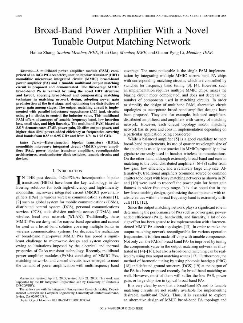
Fig. 2. Schematic of the MMIC broad-band PA.
transistor at high frequencies while maintaining the thermal sta-bility of the transistor.
III. PROPOSED PAM CONSISTING OF MMIC BROAD-BAND
PA AND TUNABLE OUTPUT MATCHING CIRCUIT
A. MMIC Broad-Band PA Design
Considering the high gain requirement of approximately30 dB at full output power levels, this MMIC broad-band PAis composed of three amplification stages and two interstagematching circuits, shown in Fig. 2. The input and interstagematching circuits are synthesized and realized on-chip. Toreduce power loss and chip area, the output matching circuit isimplemented outside of the GaAs MMIC on a module substrateto take advantages of available high- ceramic components.
3608 IEEE TRANSACTIONS ON MICROWAVE THEORY AND TECHNIQUES, VOL. 53, NO. 11, NOVEMBER 2005
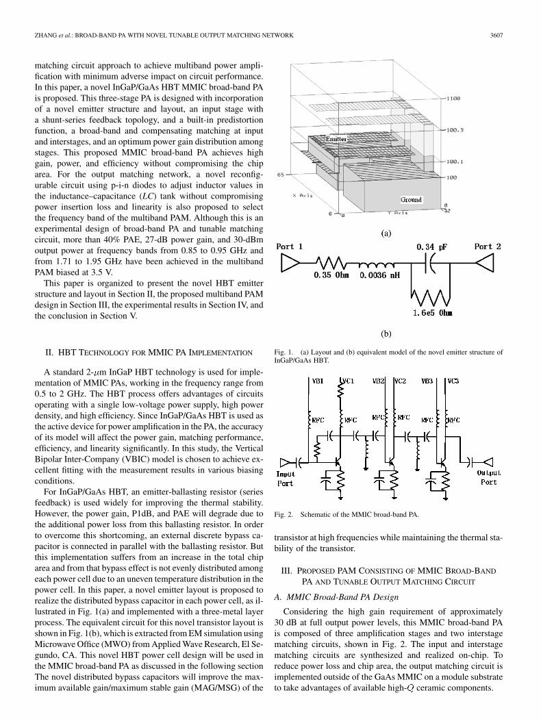
Fig. 3. Equivalent HBT nonlinear circuit for Volterra series analyses.
The distribution of the power gain among the three stages iscritical for the overall broad-band PA performance. The powergain of the first stage is compressed to get better linearity of thethree-stage PA. The second stage of the PA is designed to op-erate with high power gain and at a reasonable linearity sincethis stage is followed by an additional gain of the last stage. Toachieve better linearity, both first and second stages work in theClass A mode. Since the last stage usually dictates the overallPA efficiency, it is operated in Class AB mode to get better effi-ciency and its output matching circuit is designed to obtain max-imum power and efficiency. To achieve MMIC PA with broad-band performance, several innovative techniques have been usedin this design.
1) First Stage Design With Programmable Predistor-tion: The design of the first stage in the PA chip deservesspecial attention since this stage is critical to the perfor-mance of the entire PA. In this stage, a common emitter withresistance–capacitance (RC) shunt feedback and se-ries feedback configurations is chosen to realize broad-bandmatching at its input and output nodes and to improve circuitand thermal stability. Moreover, it is well known that owing totransistor nonlinearity the output power gain of the last stagePA decreases as its input power increases, attributing to thetypical gain compression in PAs. To overcome this problem,the first stage PA can be designed with an added predistortionfunction to compensate for the last stage gain loss at high powerlevel. This can be done by including a programmable resistorR1 in series with the inductor to adjust the biasing conditionof the first stage series and shunt feedback amplifier. As theinput power increases, the transistor initial biasing point willbe pushed from the saturation region toward the low outputcurrent and high output voltage direction [20]. Under sucha biasing arrangement, the power gain will increase under alarge input power, while it does not change under small inputpower levels. Consequently, the P1dB of the entire PA willincrease accordingly. To properly design the first stage with adesirable and controllable predistortion function, a nonlinearcircuit model at large signal conditions for the transistor needsto be used.
Volterra series is used to analyze the nonlinear effect ofthe first stage transistor. The equivalent HBT nonlinear circuitfor Volterra series analyses is shown in Fig. 3. Most reportedbipolar junction transistor (BJT)/HBT Volterra series analyses
consider the collector current only as a function of basevoltage and assume the output conductance being constant. ForInGaP/GaAs HBTs used in this paper, since the base dopinglevel 4 10 cm is much higher than the subcollectorregion 1 10 cm , the early effect is insignificant andcan be neglected in the Volterra series analysis. A third-degreeTaylor expansion of IC_VBE can be written as
(1)
where , , and are polynomial coefficients forthe transconductance. Since the nonlinear function of IC_VCEis neglected as discussed before, the equation above does nothave the polynomial coefficients for .
In HBTs, the IB_VBE nonlinearity caused by exponentialshould be considered. In theory, the IB-VBE equation should beroughly collector current divided by the current gain, but somesimplifications can be made. Since the base current does not de-pend strongly on the collector voltage, we can use a two-dimen-sional (2-D) model of , i.e.,
(2)
Here, the coefficients have similar meanings as before. Thelinear term is modeled by , and and modelits exponential curvature.
To model the capacitances, the charges at each node areextracted first and then differentiated with respect to the nodalvoltage. The extracted charge differentiated with respect totime determines the displacement current, and thus the non-linear current source. The equation shown below represents thebase-to-emitter charge as functions of base-to-emitter voltageand base-to-collector charge as functions of base-to-collectorvoltage, i.e.,
(3)
As seen from the equations, a linear C–V term is representedby and and the terms and causequadratic charge nonlinearity. Similarly, a capacitance propor-tional to ( and ) causes cubic nonlinearity.
When the InGaP/GaAs HBT technology is used here, (3) canbe further simplified. Since the base region of InGaP/GaAs HBTis heavily doped and since the thickness of the emitter region isonly tens of nanometers, the emitter layer of the HBT is alwaysdepleted even under a large signal swing. As a result, the non-linearity coming from the Cpi will not affect the performanceof the circuit greatly and is neglected when the input power isless than 0 dBm in this research. From this equation, the corre-sponding measurable capacitance and the nonlinear cur-rent source are obtained simply by differentiating thecharge equation with respect to and time, respectively, i.e.,
(4)
is simply the frequency of the distortion tone; hence, capac-itances do not cause dc distortion currents but contribute mostheavily at harmonic frequencies.
ZHANG et al.: BROAD-BAND PA WITH NOVEL TUNABLE OUTPUT MATCHING NETWORK 3609
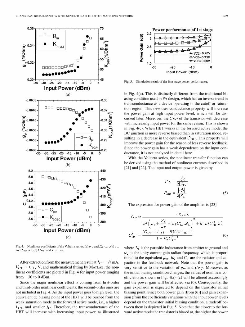
Fig. 4. Nonlinear coefficients of the Volterra series: (a) g andK , (b) gand K , (c) C and K .
After extraction from the measurement result at mA,V, and mathematical fitting by MATLAB, the non-
linear coefficients are plotted in Fig. 4 for input power rangingfrom 30 to 0 dBm.
Since the major nonlinear effect is coming from first-orderand third-order nonlinear coefficients, the second-order ones arenot included in Fig. 4. As the input power goes to high level, theequivalent dc biasing point of the HBT will be pushed from theweak saturation mode to the forward active mode, i.e., a higher
and smaller . Therefore, the transconductance of theHBT will increase with increasing input power, as illustrated
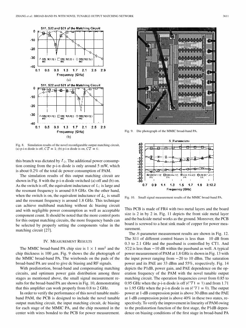
Fig. 5. Simulation result of the first stage power performance.
in Fig. 4(a). This is distinctly different from the traditional bi-asing condition used in PA design, which has an inverse trend intransconductance as a device operating in the cutoff or satura-tion region. This new trasnconductance property will increasethe power gain at high input power level, which will be dis-cussed later. Moreover, the of the transistor will decreasewith increasing input power for the same reason. This is shownin Fig. 4(c). When HBT works in the forward active mode, theBC junction is more reverse biased than in saturation mode, re-sulting in a decrease in the equivalent . This property willimprove the power gain for the reason of less reverse feedback.Since the power gain has a weak dependence on the input con-ductance, it is not analyzed in detail here.
With the Volterra series, the nonlinear transfer function canbe derived using the method of nonlinear currents described in[21] and [22]. The input and output power is given by
(5)
The expression for power gain of the amplifier is [23]
(6)
where is the parasitic inductance from emitter to ground andis the unity current gain radian frequency, which is propor-
tional to the equivalent . and are the resistor and ca-pacitor in the feedback network. Note that the power gain isvery sensitive to the variation of and . Moreover, asthe initial biasing condition changes, the values of nonlinear co-efficients as shown in Fig. 4(a)–(c) will be altered accordinglyand the power gain will be affected via (6). Consequently, thegain expansion is expected to depend on the transistor initialbiasing point. Since both power gain [from (6)] and gain expan-sion (from the coefficients variations with the input power level)depend on the transistor initial biasing condition, a tradeoff be-tween them is depicted in Fig. 5. Note that the closer to the for-ward active mode the transistor is biased at, the higher the power

3610 IEEE TRANSACTIONS ON MICROWAVE THEORY AND TECHNIQUES, VOL. 53, NO. 11, NOVEMBER 2005
Fig. 6. Schematic of the novel reconfigurable output matching circuit.
gain and the less the gain expansion can be achieved in the firststage PA.
2) Input and Interstage Matching Circuits Design: As theinput power increases, the input impedance of the first stage PAwill vary as results of the self-biasing effect. Since the shuntand series feedback topology of the amplifier is used, the inputimpedance under different power levels remains unchanged.For the input and interstage matching circuits of MMIC PA,a low-pass or high-pass filter is chosen for implementation toachieve broad-band performance. Furthermore, the reactiveelements are primarily used here to lower the power insertionloss as an alternative to the lossy matching technique generallyused in broad-band amplifier design. Note that the frequencyresponse of these matching circuits is also designed to tailortheir characteristics for complementing that of the active de-vices, leading to further gain flatness in a broad frequencyrange, known as the compensating matching technique. Forthe last stage of the MMIC PA, its transistor layout and inputnetwork are realized in the distributed fashion, which is suitablefor broad-band matching, evenly distributing RF power andstabilizing its dc biasing condition.
B. Tunable Output Matching Network
The proposed PAM is composed of an MMIC broad-band PAand a tunable output matching circuit with a voltage control port.Since the input impedance of the MMIC PA can be designedclose to 50 , the input matching circuit is easy to be designedin broad-band with a fixing value of its components.
It is noted that the output matching circuit is typically re-alized by either a low-pass or a high-pass filter, and that theoutput impedance of the MMIC broad-band PA is generallymuch lower than 50 . To optimize the power transfer, oneneeds to adjust the component values in the output matchingcircuit of the multiband PAM to satisfy the impedance transfor-mation ratio requirement at various frequencies. The schematicof the novel tunable output matching circuit is realized by a low-pass filter with the control port (CT1), as illustrated in Fig. 6.This -match network decouples requirement from the trans-formation ratio by introducing an intermediate resistance valueto transform to, allowing us to achieve a much higher than isgenerally available from the simple L-match. The values of ,
Fig. 7. Frequency tuning range with normalized C1 and C2.
, and determine the resonant frequency, value, and theimpedance transform ratio.
A typical implementation of the -match network circuit is tochoose a fixed value of inductor while adjusting the capacitancevalue by using varactors. However, such an implementationlimits the tunable frequency range, impedance transformationratio, optimum output power, and power efficiency matching.To achieve the specific design of frequency tuning range of0.8 to 2.0 GHz, the capacitance ratios of maxim to minimum
and are determined to be 7.5 and 100, respectively, asshown in Fig. 7. The values of normalized and are set at0.9-GHz resonant frequency. Such a high value of capacitanceratio is beyond the achievable capacitive tuning of any varac-tors. On the other hand, such a frequency tuning requirementcan be implemented with tunable inductors, demanding its ratioof maximum to minimum of only 5. In this case, the values ofthe capacitors in the output matching circuit are preselected fora specific design. For the adjustable inductor, a p-i-n diode isused in this paper to control the equivalent inductance between
and , consequently changing the resonant frequency andthe impedance transformation ratio.
To achieve dual-band applications, there are four capacitors,four inductors, and one p-i-n diode included in this novel recon-figurable output matching circuit, while the conventional oneneeds at least six capacitors and four inductors [4]. Comparedto the traditional implementation of adjustable inductors, ourcircuit topology neither suffers from power and frequency limi-tations [24], [25] nor requires a big chip area [26]. As comparedto the conventional implementation of tunable matching circuitsusing switches to rout the signal paths at different frequencybands, this novel output matching circuit uses only about half ofthe component counts for dual-band applications and one fourthof that for quad-band applications. Consequently, it reduces themodule size, weight, and cost. Moreover, since the p-i-n diodeis in one branch of the output matching circuit, only part of thesignal will pass through the p-i-n diode, thus resulting in lesspower insertion loss and degradation in linearity in the matchingcircuit than the conventional one. It is worth mentioning that the
value of is much lower than that of the p-i-n diode and(a bypassing capacitor), suggesting the equivalent value of
ZHANG et al.: BROAD-BAND PA WITH NOVEL TUNABLE OUTPUT MATCHING NETWORK 3611
Fig. 8. Simulation results of the novel reconfigurable output matching circuit,(a) p-i-n diode is off, CT = 1; (b) p-i-n diode is on, CT = 0.
this branch was dictated by . The additional power consump-tion coming from the p-i-n diode is only around 5 mW, whichis about 0.2% of the total dc power consumption of PAM.
The simulation results of this output matching circuit areshown in Fig. 8 with the p-i-n diode switched (a) off and (b) on.As the switch is off, the equivalent inductance of is large andthe resonant frequency is around 0.9 GHz. On the other hand,when the switch is on, the equivalent inductance of is smalland the resonant frequency is around 1.8 GHz. This techniquecan achieve multiband matching without dc biasing circuitand with negligible power consumption as well as acceptablecomponent count. It should be noted that the more control portsfor this output matching circuits, the more frequency bands canbe selected by properly setting the components value in thematching circuit [27].
IV. MEASUREMENT RESULTS
The MMIC broad-band PA chip size is 1 1 mm and thechip thickness is 100 m. Fig. 9 shows the die photograph ofthe MMIC broad-band PA. The wirebonds on the pads of thebroad-band PA are used to give dc biasing and RF signals.
With predistortion, broad-band and compensating matchingcircuits, and optimum power gain distribution among threestages as mentioned above, the small signal measurement re-sults for the broad-band PA are shown in Fig. 10, demonstratingthat this amplifier can work properly from 0.8 to 2 GHz.
In order to verify the performance of this novel tunable multi-band PAM, the PCB is designed to include the novel tunableoutput matching circuit, the input matching circuit, dc biasingfor each stage of the MMIC PA, and the chip mounted in thecenter with wires bonded to the PCB for power measurement.
Fig. 9. Die photograph of the MMIC broad-band PA.
Fig. 10. Small signal measurement results of the MMIC broad-band PA.
This PCB is made of FR4 with two metal layers and the boardsize is 2 in by 2 in. Fig. 11 depicts the front side metal layerand the backside metal works as the ground. Moreover, the PCBboard is screwed to a heat sink made of copper for power mea-surement.
The -parameter measurement results are shown in Fig. 12.The S11 of different control biases is less than 10 dB from0.3 to 2.1 GHz and the passband is controlled by CT1. And
is less than 10 dB within the passband as well. A typicalpower measurement of PAM at 1.8 GHz is shown in Fig. 13 withthe input power ranging from 20 to 10 dBm. The saturationpower and its PAE are 33 dBm and 55%, respectively. Fig. 14depicts the P1dB, power gain, and PAE dependence on the op-eration frequency of the PAM with the novel tunable outputmatching circuit. The operation frequencies cover from 0.85 to0.95 GHz when the p-i-n diode is off ( ) and from 1.71to 1.95 GHz when the p-i-n diode is on ( ). The outputpower at 1-dB compression point is above 30 dBm and the PAEat 1-dB compression point is above 40% in these two states, re-spectively. To verify the improvement in linearity of PAM owingto the predistortion function of the first stage, the P1dB depen-dence on biasing conditions of the first stage in broad-band PA

3612 IEEE TRANSACTIONS ON MICROWAVE THEORY AND TECHNIQUES, VOL. 53, NO. 11, NOVEMBER 2005
Fig. 11. PCB board for power measurement of multiband PAM.
Fig. 12. S-parameter measurement results of the multiband PAM with thenovel tunable output matching circuit.
is measured and compared in Table I. By adjusting the resistorvalue of the first stage, is gradually reduced implying HBToperating closer to weak saturation and leading to improvementin P1dB as predicated in Fig. 5. It is noted that 3–4 dB of im-provement is measured as the result of the predistortion functionprovided by the first stage series-shunt feedback amplifier. Themeasurement results demonstrate that the tunable PAM func-tions well and that multiband operation can be achieved with a
Fig. 13. Power measurement results of the multiband PAM at 1.8 GHz.
Fig. 14. Power measurement results of the multiband PAM with the noveltunable output matching circuit.
TABLE IP1dB COMPARISON OF PAM WITH DIFFERENT BIASING
CONDITIONS IN THE FIRST STAGE
single MMIC PA chip and a single matching circuit. Comparedwith conventional multiband PA solutions [4], [28], which usedtwo narrow-band PA chips and two matching circuits to achievemultiband performance, our design realized it with a smallerchip area and one external matching circuit. However, our tun-able PAM requires an additional control circuit for frequencyselection. Furthermore, the power insertion loss from the output
ZHANG et al.: BROAD-BAND PA WITH NOVEL TUNABLE OUTPUT MATCHING NETWORK 3613
matching circuit is about 0.1 dB larger than that from the con-ventional narrow-band matching ones. Lastly, while the nonlin-earity attributed to the p-i-n diode in the output matching circuitis expected to affect performance of the PAM, it is not as badas one may think as evident by the measurement results. It isworthwhile mentioning that if conventional varactors were usedin the output matching circuit to adjust the capacitance value forfrequency tuning, it results in an even worse performance thanours owing to additional phase modulation.
V. CONCLUSION
An InGaP/GaAs HBT MMIC broad-band PA is developed byusing the novel HBT structure and layout, predistortion at theinput stage, broad-band and compensating matching circuits,and optimum power gain distribution. A novel tunable outputmatching circuit for multiband PAM operating at dual frequencybands by using adjustable inductors controlled by p-i-n diode isdemonstrated. The working frequency of the multiband PAMcan be programmed by this novel matching circuit, thus real-izing a single MMIC PA with a single matching circuit to covermultiband wireless communications.
REFERENCES
[1] P. Asbeck, G. Hanington, P. F. Chen, and L. Larson, “Efficiency and lin-earity improvement in power amplifiers for wireless communications,”in IEEE Gallium Arsenide Integrated Circuit Symp., Atlanta, GA, Nov.1998, pp. 15–18.
[2] W. Kim, S. Kang, K. Lee, M. Chung, J. Kang, and B. Kim, “Analysis ofnonlinear behavior of power HBTs,” IEEE Trans. Microw. Theory Tech.,vol. 50, no. 7, pp. 1714–1722, Jul. 2002.
[3] K. Yamamoto, T. Shimura, T. Asada, T. Okuda, K. Mori, K. Choumei,S. Suzuki, T. Miura, S. Fujimoto, R. Hattori, H. Nakano, K. Hosogi, J.Otsuji, A. Inoue, K. Yajima, T. Ogata, Y. Mijazaki, and M. Yamanouchi,“A 3.2-V operation single-chip AlGaAs/GaAs HBT MMIC power am-plifier for GSM900/1800 dual-band applications,” in IEEE MTT-S Int.Microwave Symp. Dig., vol. 4, Anaheim, CA, Jun. 1999, pp. 1397–1400.
[4] S. Zhang, P. Betchko, J. Mokoro, and R. McMorrow, “A novel poweramplifier module for quad-band wireless handset applications,” in IEEERadio Frequency Integrated Circuits Symp., Philadelphia, PA, Jun. 2003,pp. 129–132.
[5] T. Cegielski and R. Matuszewski, “The design of medium powerC-bandbalanced amplifiers,” in 15th Int. Conf. Radar Wireless Communications,vol. 1, Warsaw, Poland, May 2004, pp. 107–110.
[6] W. S. Percival, “Thermionic valve circuits,” British Patent 460 562, Jul.24, 1936.
[7] E. W. Strid and K. R. Gleeson, “A DC–12 GHz monolithic GaAs FETdistributed amplifier,” IEEE Trans. Microw. Theory Tech., vol. MTT-30,no. 7, pp. 969–975, Jul. 1982.
[8] K. W. Eccleston, “Compact dual-fed distributed power amplifier,” IEEETrans. Microw. Theory Tech., vol. 53, no. 3, pp. 825–831, Mar. 2005.
[9] T. Arell and T. Hongsmatip, “A unique MMIC broad-band poweramplifier approach,” IEEE J. Solid-State Circuits, vol. 28, no. 10, pp.1005–1010, Oct. 1993.
[10] X. Zhu, X. Chen, and J. Ling, “2–6 GHz GaAs MMIC power amplifier,”in Proc. Int. Microwave and Millimeter Wave Technology Conf., Beijing,China, Sep. 2000, pp. 134–137.
[11] I. J. Bahl, “Low loss matching (LLM) design technique for power am-plifiers,” IEEE Micro, vol. 5, no. 4, pp. 66–71, Dec. 2004.
[12] S. Nam, S. Miya, M. Ozaki, and I. D. Robertson, “A comparison oftopologies for single-ended millimeter-wave monolithic amplifier de-sign,” in IEEE MTT-S Int. Microwave Symp. Dig., vol. 2, Baltimore, MD,Jun. 1998, pp. 677–680.
[13] J. J. Komiak, “Power amplifier for broad band operation at frequenciesabove one GHz and at decade watt power levels,” U.S. Patent 5 111 157,May 1, 1991.
[14] S. Kim, J. Lee, J. Shin, and B. Kim, “CDMA handset power amplifierwith a switched output matching circuit for low/high power mode oper-ations,” in IEEE MTT-S Int. Microwave Symp. Dig., vol. 3, Fort Worth,TX, Jun. 2004, pp. 1523–1526.
[15] A. C. Cotler and E. R. Brown, “The feasibility of a variable outputmatching circuit in a high-power SSPA,” in IEEE Radio Wireless Conf.,Boston, MA, Aug. 2002, pp. 189–191.
[16] J. J. Yao, C. W. Seabury, D. R. Pehlke, J. L. Bartlett, J. L. Julian, M.C. F. Chang, H. O. Marcy, K. D. Pedrotti, and D. Mehrotra, “Integratedtunable high efficiency power amplifier,” U.S. Patent 6 232 841, May 15,2001.
[17] R. D. Boesch and K. P. Conroy, “Impedance matching for power ampli-fier,” U.S. Patent 5 969 582, Oct. 19, 1999.
[18] M. L. Her, Y. C. Chiou, Y. Z. Wang, Y. L. Wang, P. T. Sun, K. Y. Lin, C. A.Wang, and Q. M. Lin, “Broad-band power amplifier with an improveddoubly tapered periodic bandgap PBG structure for harmonic tuning,”in 8th Int. Communication Systems Conf., Singapore, Nov. 2002, pp.21–24.
[19] S. G. Jeong, D. K. Hwang, Y. C. Jeong, and C. D. Kim, “Amplifier de-sign using �=4 high impedance bias line with defect ground structure(DGS),” in IEEE MTT-S Int. Microwave Symp. Dig., vol. 2, Seattle, WA,Jun. 2002, pp. 1161–1164.
[20] M. Shigaki and T. Sasaki, “Linearizer for power amplifier,” U.S. Patent6 377 118, Apr. 23, 2002.
[21] S. A. Maas, Nonlinear Microwave Circuits. Norwood, MA: ArtechHouse, 1988.
[22] P. Wambacq and W. Sansen, Distortion Analysis of Analog IntegratedCircuits. Norwell, MA: Kluwer, 1998.
[23] J. Deng, P. S. Gudem, L. Larson, and P. M. Asbeck, “A high average-effi-ciency SiGe HBT power amplifier for WCDMA handset applications,”IEEE Trans. Microw. Theory Tech., vol. 53, no. 2, pp. 529–537, Feb.2005.
[24] K. W. Kobayashi, A. K. Oki, D. K. Umemoto, T. R. Block, and D. C.Streit, “A novel self-oscillating HEMT-HBT cascode VCO-mixer usingan active tunable inductor,” IEEE J. Solid-State Circuits, vol. 33, no. 6,pp. 870–876, Jun. 1998.
[25] R. L. Brandt, “Orthogonal-electrically variable magnetic device,” U.S.Patent 5 534 837, Jul. 9, 1996.
[26] S. Zhou, X. Q. Sun, and W. N. Carr, “A micro variable inductor chipusing MEMS relays,” in Int. Solid State Sensors and Actuators Conf.,Chicago, IL, Jun. 1997, pp. 1137–1140.
[27] H. Zhang, H. Gao, and G. P. Li, “A novel tunable broad-band poweramplifier module operating from 0.8 GHz to 2.0 GHz,” in IEEE MTT-SInt. Microwave Symp. Dig., Long Beach, CA, Jun. 2005. [CD ROM].
[28] P. Savary, A. Girardot, G. Montoriol, F. Dupis, B. Thibaud, R. Jaoui,L. Chapoux, V. Esnault, L. Cornibert, O. Izumi, D. Hill, M. Sadaka,H. Henry, E. Yu, M. Tutt, M. Majerus, R. Uscola, F. Clayton, C. Ram-pley, S. Klingbeil, K. Rajagopalan, A. Mitra, and A. Reyes, “Dual-bandmulti-mode power amplifier module using a third generation HBT tech-nology,” in IEEE Gallium Arsenide Integrated Circuit Symp., Baltimore,MD, Oct. 2001, pp. 71–74.
Haitao Zhang (S’04) received the B.S. and M.S. de-grees in electrical engineering from Tsinghua Uni-versity, Beijing, China, in 1999 and 2002, and is cur-rently working toward the Ph.D. degree at the Univer-sity of California at Irvine (UCI). His doctoral disser-tation concerns device modeling, thermal and distor-tion characteristics of HBTs, and their applicationsto high-linearity, high-efficiency, and broad-band PAdesign.
Huai Gao (M’02) received the B.S., M.S., and Ph.D. degrees in electronic en-gineering from Nanjing University, Nanjing, China, in 1983, 1993, and 2001,respectively.
Since 2002, he has been with the Integrated Nanosystems Research Facility,University of California at Irvine. His research interest is on RF integrated cir-cuit (RFIC) and MMIC design.
3614 IEEE TRANSACTIONS ON MICROWAVE THEORY AND TECHNIQUES, VOL. 53, NO. 11, NOVEMBER 2005
Guann-Pyng Li (M’83) was previously involvedwith the development of a silicon silicide molecularbeam epitaxy (MBE) system while with the Uni-versity of California at Los Angeles (UCLA), andthen in the areas of silicon bipolar very large scaleintegration (VLSI) technology and process-relateddevice physics while with the IBM T. J. Watson Re-search Center. From 1983 to 1988, during his tenureas a Staff Member and Manger of the TechnologyGroup with IBM, he coordinated and conductedresearch efforts in technology development of
high-performance and scaled-dimension (0.5 and 0.25 �m) bipolar/bipolarcomplementary metal–oxide–semiconductor (BiCMOS) devices and integratedcircuits (ICs), as well as research into optical switches and opto-electronicsfor ultra-high-speed IC measurements. In 1987, he also chaired the committeefor defining IBM semiconductor technology roadmap for beyond year 2000.He also led a research/development team to transfer the semiconductor chiptechnology to manufacturing in IBM. He is currently a Professor with theUniversity of California at Irvine (UCI), with appointments with the De-partment of Electrical Engineering and Computer Science, Department ofChemical Engineering and Materials Science, and Department of BiomedicalEngineering. He is also the Director of the Integrated Nanosystems ResearchFacility, Henry Samueli School of Engineering, UCI. He heads major researchprograms in microelectromechanical system (MEMS), microelectronics, andBioMEMS. He has authored or coauthored over 200 research papers involvingsemiconductor materials/devices/technologies, polymer-based BioMEMSsystems, bionanotechnology, RF-MEMS communication systems, and mixeddigital/analog/microwave circuit systems. His current research interests includemicrofluidic lab-on-a-chip design/fabrication for nanomedicine and biosensingapplications and high-speed electronic/opto-electronic devices and circuits fornetwork and wireless communication applications.
Prof. Li was the recipient of a 1987 Outstanding Research ContributionAward presented by IBM and a 1997 and 2001 Outstanding EngineeringProfessor Award presented by UCI.


![RF circuits design 6ue.pwr.wroc.pl/.../lecture/RF_circuits_design_6.pdfAmplifier block diagram RF transistor [S] Output matching circuit Input matching circuit BIAS circuit ZG ZL Amplifier](https://img.pdfslide.us/doc/110x75/5e41026cfd4507719c31d8c5/rf-circuits-design-6uepwrwrocpllecturerfcircuitsdesign6pdf-amplifier.jpg)