Embed Size (px)
Citation preview
Use of Bridgetek devices in life support and/or safety applications is entirely at the user’s risk, and the user agrees to defend, indemnify and hold Bridgetek harmless from any and all damages,
claims, suits or expense resulting from such use.
Bridgetek Pte Ltd (BRTChip) 178 Paya Lebar Road, #07-03, Singapore 409030
Tel: +65 6547 4827 Fax: +65 6841 6071
Web Site: http://www.brtchip.com Copyright © Bridgetek Pte Ltd
Technical Note
BRT_TN_004
Bridgetek Example IC PCB
Footprints
Version 1.0
Issue Date: 2019-06-14
This Technical Note shows examples of Bridgetek IC PCB footprints which can be used as a guide for creating your own IC PCB footprints.
2 Product Page
Document Feedback Copyright © Bridgetek Pte Ltd
Technical Note
BRT_TN_004 Bridgetek Example IC PCB Footprints Version 1.0
Document No.: BRT_000259 Clearance No.: BRT#138
Table of Contents
1 Introduction .............................................................. 4
1.1 Scope .................................................................................. 4
1.1.1 Unavailable Footprints ......................................................................... 4
2 All Scaled Footprints .................................................. 5
2.1 QFP Packages ...................................................................... 5
2.2 QFN Packages...................................................................... 5
3 Packages by Product ................................................. 6
3.1 QFP Packages ...................................................................... 6
3.2 QFN Packages...................................................................... 6
4 48-pin VQFN (7mm x 7mm) ....................................... 7
4.1 Scaled Footprint .................................................................. 7
4.2 Annotated Footprint ............................................................ 7
5 48-pin QFN (7mm x 7mm) ......................................... 8
5.1 Scaled Footprint .................................................................. 8
5.2 Annotated Footprint ............................................................ 8
6 56-pin VQFN (8mm x 8mm) ....................................... 9
6.1 Scaled Footprint .................................................................. 9
6.2 Annotated Footprint ............................................................ 9
7 64-pin VQFN (9mm x 9mm) ..................................... 10
7.1 Scaled Footprint ................................................................ 10
7.2 Annotated Footprint .......................................................... 10
8 68-pin QFN (8mm x 8mm) ....................................... 11
8.1 Scaled Footprint ................................................................ 11
8.2 Annotated Footprint .......................................................... 11
9 76-pin QFN .............................................................. 12
9.1 Scaled Footprint ................................................................ 12
9.2 Annotated Footprint .......................................................... 12
10 80-pin LQFP ........................................................... 13

3 Product Page
Document Feedback Copyright © Bridgetek Pte Ltd
Technical Note
BRT_TN_004 Bridgetek Example IC PCB Footprints Version 1.0
Document No.: BRT_000259 Clearance No.: BRT#138
10.1 Scaled Footprint .............................................................. 13
10.2 Annotated Footprint ........................................................ 13
11 100-pin LQFP ......................................................... 14
11.1 Scaled Footprint .............................................................. 14
11.2 Annotated Footprint ........................................................ 14
12 100-pin QFN .......................................................... 15
12.1 Scaled Footprint .............................................................. 15
12.2 Annotated Footprint ........................................................ 15
13 Contact Information .............................................. 16
Appendix A– References .............................................. 17
Document References ............................................................... 17
Acronyms and Abbreviations ..................................................... 17
Appendix B – List of Tables & Figures .......................... 18
List of Tables ............................................................................. 18
List of Figures ........................................................................... 18
Appendix C– Revision History ...................................... 19
4 Product Page
Document Feedback Copyright © Bridgetek Pte Ltd
Technical Note
BRT_TN_004 Bridgetek Example IC PCB Footprints Version 1.0
Document No.: BRT_000259 Clearance No.: BRT#138
1 Introduction
This Technical Note shows examples of Bridgetek IC PCB footprints which can be used as a guide for creating your own PCB footprints. The IC footprints in this document are sourced from various Bridgetek hardware such as development modules and demo hardware, using the most common and cost effective package types.
Most Bridgetek IC footprints are included in this document; however some are missing when a package type has not been used for specific Bridgetek hardware. See Table 1.1 for unavailable footprints. The IC footprints in this document provide:
A 1:1 scaled IC footprint An annotated IC footprint showing some key measurements
All dimensions shown are in millimetres (mm). Additionally, a range of IC solutions from Bridgetek are available through AltiumLive.
To view Altium files, you need either the full version of ‘Altium Designer’, or ‘Altium Viewer’ which can be downloaded for free from Altium’s web site. Note that all IC footprints may not be available through AltiumLive. Please contact Bridgetek in this case.
1.1 Scope
These IC PCB footprints can be used as a guide to create your own IC PCB footprints with particular PCB design tools other than Altium.
Please refer to the IC datasheet for full IC package parameters.
Note: No guarantees can be provided in this document. These can be used as a guide only. Note: Bridgetek modules are recommended for product test and development prior to custom hardware development.
1.1.1 Unavailable Footprints
Table 1.1 shows that there is one footprint not included in this document as, for example, it has never been used for specific hardware developments within Bridgetek. Other package options are available for this product family and are included in this document.
Note: This is correct at the time of writing and newer products may not be included.
Package Part Numbers
QFN-56 FT931Q
Table 1.1 Unavailable Footprints
5 Product Page
Document Feedback Copyright © Bridgetek Pte Ltd
Technical Note
BRT_TN_004 Bridgetek Example IC PCB Footprints Version 1.0
Document No.: BRT_000259 Clearance No.: BRT#138
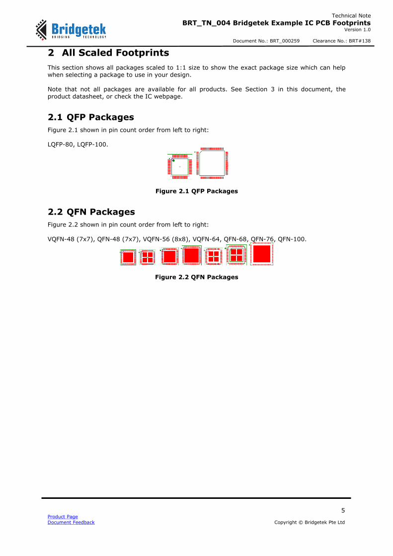
2 All Scaled Footprints
This section shows all packages scaled to 1:1 size to show the exact package size which can help when selecting a package to use in your design. Note that not all packages are available for all products. See Section 3 in this document, the product datasheet, or check the IC webpage.
2.1 QFP Packages
Figure 2.1 shown in pin count order from left to right: LQFP-80, LQFP-100.
Figure 2.1 QFP Packages
2.2 QFN Packages
Figure 2.2 shown in pin count order from left to right:
VQFN-48 (7x7), QFN-48 (7x7), VQFN-56 (8x8), VQFN-64, QFN-68, QFN-76, QFN-100.
Figure 2.2 QFN Packages
6 Product Page
Document Feedback Copyright © Bridgetek Pte Ltd
Technical Note
BRT_TN_004 Bridgetek Example IC PCB Footprints Version 1.0
Document No.: BRT_000259 Clearance No.: BRT#138
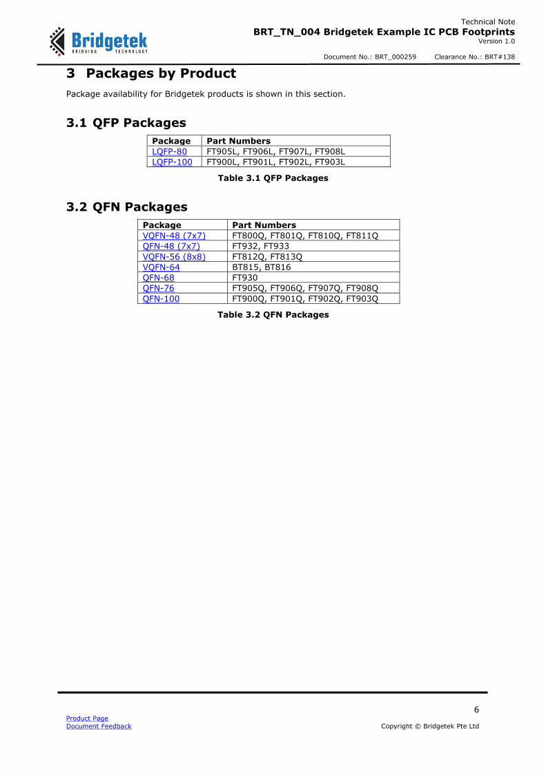
3 Packages by Product
Package availability for Bridgetek products is shown in this section.
3.1 QFP Packages
Package Part Numbers
LQFP-80 FT905L, FT906L, FT907L, FT908L
LQFP-100 FT900L, FT901L, FT902L, FT903L
Table 3.1 QFP Packages
3.2 QFN Packages
Package Part Numbers
VQFN-48 (7x7) FT800Q, FT801Q, FT810Q, FT811Q
QFN-48 (7x7) FT932, FT933
VQFN-56 (8x8) FT812Q, FT813Q
VQFN-64 BT815, BT816
QFN-68 FT930
QFN-76 FT905Q, FT906Q, FT907Q, FT908Q
QFN-100 FT900Q, FT901Q, FT902Q, FT903Q
Table 3.2 QFN Packages
7 Product Page
Document Feedback Copyright © Bridgetek Pte Ltd
Technical Note
BRT_TN_004 Bridgetek Example IC PCB Footprints Version 1.0
Document No.: BRT_000259 Clearance No.: BRT#138
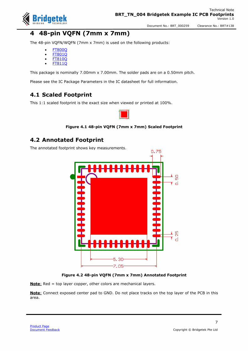
4 48-pin VQFN (7mm x 7mm)
The 48-pin VQFN/WQFN (7mm x 7mm) is used on the following products:
FT800Q FT801Q FT810Q FT811Q
This package is nominally 7.00mm x 7.00mm. The solder pads are on a 0.50mm pitch. Please see the IC Package Parameters in the IC datasheet for full information.
4.1 Scaled Footprint
This 1:1 scaled footprint is the exact size when viewed or printed at 100%.
Figure 4.1 48-pin VQFN (7mm x 7mm) Scaled Footprint
4.2 Annotated Footprint
The annotated footprint shows key measurements.
Figure 4.2 48-pin VQFN (7mm x 7mm) Annotated Footprint
Note: Red = top layer copper, other colors are mechanical layers.
Note: Connect exposed center pad to GND. Do not place tracks on the top layer of the PCB in this area.
8 Product Page
Document Feedback Copyright © Bridgetek Pte Ltd
Technical Note
BRT_TN_004 Bridgetek Example IC PCB Footprints Version 1.0
Document No.: BRT_000259 Clearance No.: BRT#138
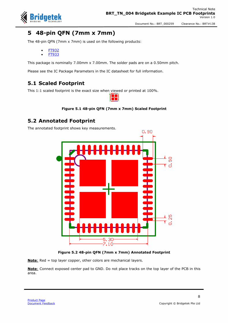
5 48-pin QFN (7mm x 7mm)
The 48-pin QFN (7mm x 7mm) is used on the following products:
FT932 FT933
This package is nominally 7.00mm x 7.00mm. The solder pads are on a 0.50mm pitch.
Please see the IC Package Parameters in the IC datasheet for full information.
5.1 Scaled Footprint
This 1:1 scaled footprint is the exact size when viewed or printed at 100%.
Figure 5.1 48-pin QFN (7mm x 7mm) Scaled Footprint
5.2 Annotated Footprint
The annotated footprint shows key measurements.
Figure 5.2 48-pin QFN (7mm x 7mm) Annotated Footprint
Note: Red = top layer copper, other colors are mechanical layers. Note: Connect exposed center pad to GND. Do not place tracks on the top layer of the PCB in this area.
9 Product Page
Document Feedback Copyright © Bridgetek Pte Ltd
Technical Note
BRT_TN_004 Bridgetek Example IC PCB Footprints Version 1.0
Document No.: BRT_000259 Clearance No.: BRT#138
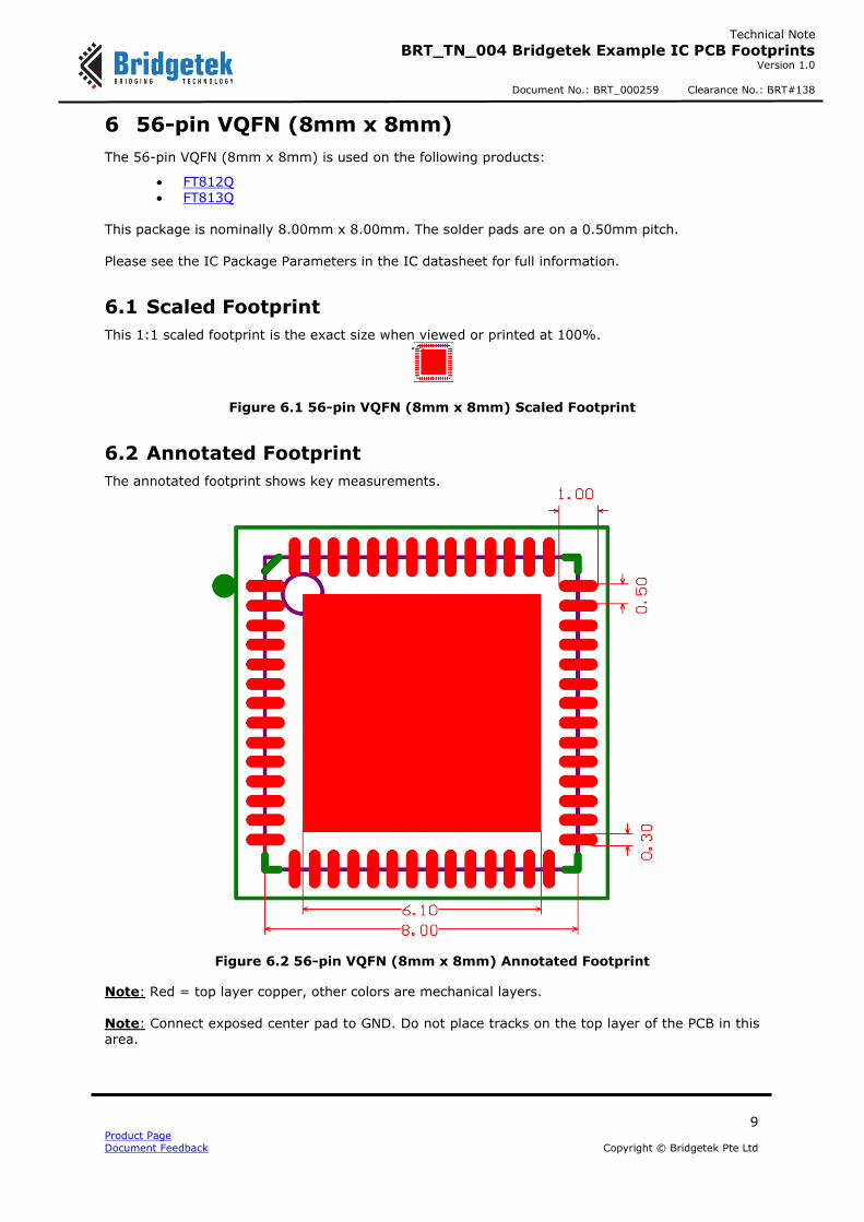
6 56-pin VQFN (8mm x 8mm)
The 56-pin VQFN (8mm x 8mm) is used on the following products:
FT812Q FT813Q
This package is nominally 8.00mm x 8.00mm. The solder pads are on a 0.50mm pitch.
Please see the IC Package Parameters in the IC datasheet for full information.
6.1 Scaled Footprint
This 1:1 scaled footprint is the exact size when viewed or printed at 100%.
Figure 6.1 56-pin VQFN (8mm x 8mm) Scaled Footprint
6.2 Annotated Footprint
The annotated footprint shows key measurements.
Figure 6.2 56-pin VQFN (8mm x 8mm) Annotated Footprint
Note: Red = top layer copper, other colors are mechanical layers. Note: Connect exposed center pad to GND. Do not place tracks on the top layer of the PCB in this area.
10 Product Page
Document Feedback Copyright © Bridgetek Pte Ltd
Technical Note
BRT_TN_004 Bridgetek Example IC PCB Footprints Version 1.0
Document No.: BRT_000259 Clearance No.: BRT#138
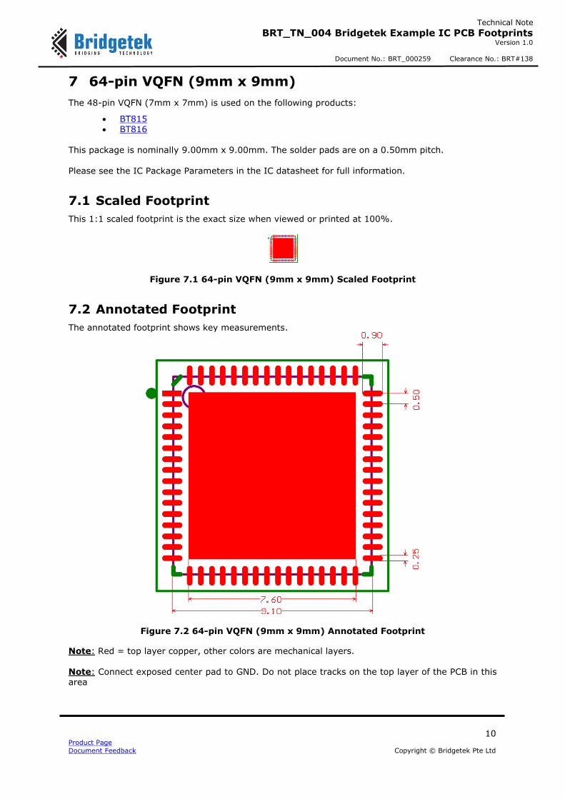
7 64-pin VQFN (9mm x 9mm)
The 48-pin VQFN (7mm x 7mm) is used on the following products:
BT815 BT816
This package is nominally 9.00mm x 9.00mm. The solder pads are on a 0.50mm pitch.
Please see the IC Package Parameters in the IC datasheet for full information.
7.1 Scaled Footprint
This 1:1 scaled footprint is the exact size when viewed or printed at 100%.
Figure 7.1 64-pin VQFN (9mm x 9mm) Scaled Footprint
7.2 Annotated Footprint
The annotated footprint shows key measurements.
Figure 7.2 64-pin VQFN (9mm x 9mm) Annotated Footprint
Note: Red = top layer copper, other colors are mechanical layers. Note: Connect exposed center pad to GND. Do not place tracks on the top layer of the PCB in this area
11 Product Page
Document Feedback Copyright © Bridgetek Pte Ltd
Technical Note
BRT_TN_004 Bridgetek Example IC PCB Footprints Version 1.0
Document No.: BRT_000259 Clearance No.: BRT#138
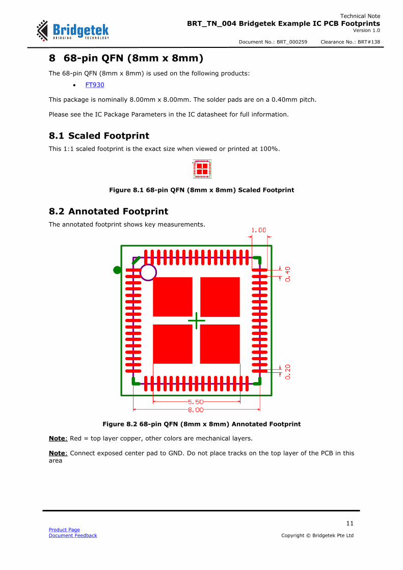
8 68-pin QFN (8mm x 8mm)
The 68-pin QFN (8mm x 8mm) is used on the following products:
FT930
This package is nominally 8.00mm x 8.00mm. The solder pads are on a 0.40mm pitch. Please see the IC Package Parameters in the IC datasheet for full information.
8.1 Scaled Footprint
This 1:1 scaled footprint is the exact size when viewed or printed at 100%.
Figure 8.1 68-pin QFN (8mm x 8mm) Scaled Footprint
8.2 Annotated Footprint
The annotated footprint shows key measurements.
Figure 8.2 68-pin QFN (8mm x 8mm) Annotated Footprint
Note: Red = top layer copper, other colors are mechanical layers. Note: Connect exposed center pad to GND. Do not place tracks on the top layer of the PCB in this area
12 Product Page
Document Feedback Copyright © Bridgetek Pte Ltd
Technical Note
BRT_TN_004 Bridgetek Example IC PCB Footprints Version 1.0
Document No.: BRT_000259 Clearance No.: BRT#138
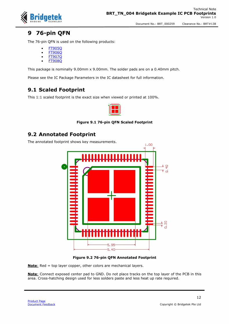
9 76-pin QFN
The 76-pin QFN is used on the following products:
FT905Q FT906Q FT907Q FT908Q
This package is nominally 9.00mm x 9.00mm. The solder pads are on a 0.40mm pitch. Please see the IC Package Parameters in the IC datasheet for full information.
9.1 Scaled Footprint
This 1:1 scaled footprint is the exact size when viewed or printed at 100%.
Figure 9.1 76-pin QFN Scaled Footprint
9.2 Annotated Footprint
The annotated footprint shows key measurements.
Figure 9.2 76-pin QFN Annotated Footprint
Note: Red = top layer copper, other colors are mechanical layers. Note: Connect exposed center pad to GND. Do not place tracks on the top layer of the PCB in this area. Cross-hatching design used for less solders paste and less heat up rate required.
13 Product Page
Document Feedback Copyright © Bridgetek Pte Ltd
Technical Note
BRT_TN_004 Bridgetek Example IC PCB Footprints Version 1.0
Document No.: BRT_000259 Clearance No.: BRT#138
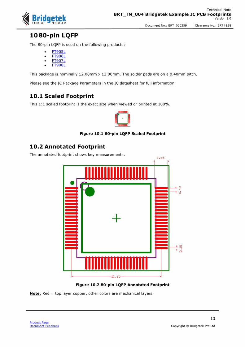
10 80-pin LQFP
The 80-pin LQFP is used on the following products:
FT905L FT906L FT907L FT908L
This package is nominally 12.00mm x 12.00mm. The solder pads are on a 0.40mm pitch. Please see the IC Package Parameters in the IC datasheet for full information.
10.1 Scaled Footprint
This 1:1 scaled footprint is the exact size when viewed or printed at 100%.
Figure 10.1 80-pin LQFP Scaled Footprint
10.2 Annotated Footprint
The annotated footprint shows key measurements.
Figure 10.2 80-pin LQFP Annotated Footprint
Note: Red = top layer copper, other colors are mechanical layers.
14 Product Page
Document Feedback Copyright © Bridgetek Pte Ltd
Technical Note
BRT_TN_004 Bridgetek Example IC PCB Footprints Version 1.0
Document No.: BRT_000259 Clearance No.: BRT#138
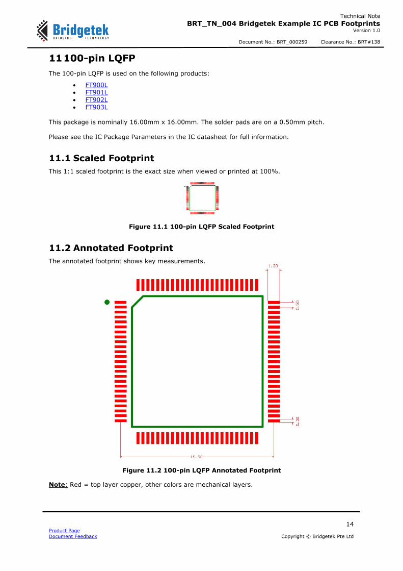
11 100-pin LQFP
The 100-pin LQFP is used on the following products:
FT900L FT901L FT902L FT903L
This package is nominally 16.00mm x 16.00mm. The solder pads are on a 0.50mm pitch. Please see the IC Package Parameters in the IC datasheet for full information.
11.1 Scaled Footprint
This 1:1 scaled footprint is the exact size when viewed or printed at 100%.
Figure 11.1 100-pin LQFP Scaled Footprint
11.2 Annotated Footprint
The annotated footprint shows key measurements.
Figure 11.2 100-pin LQFP Annotated Footprint
Note: Red = top layer copper, other colors are mechanical layers.
15 Product Page
Document Feedback Copyright © Bridgetek Pte Ltd
Technical Note
BRT_TN_004 Bridgetek Example IC PCB Footprints Version 1.0
Document No.: BRT_000259 Clearance No.: BRT#138
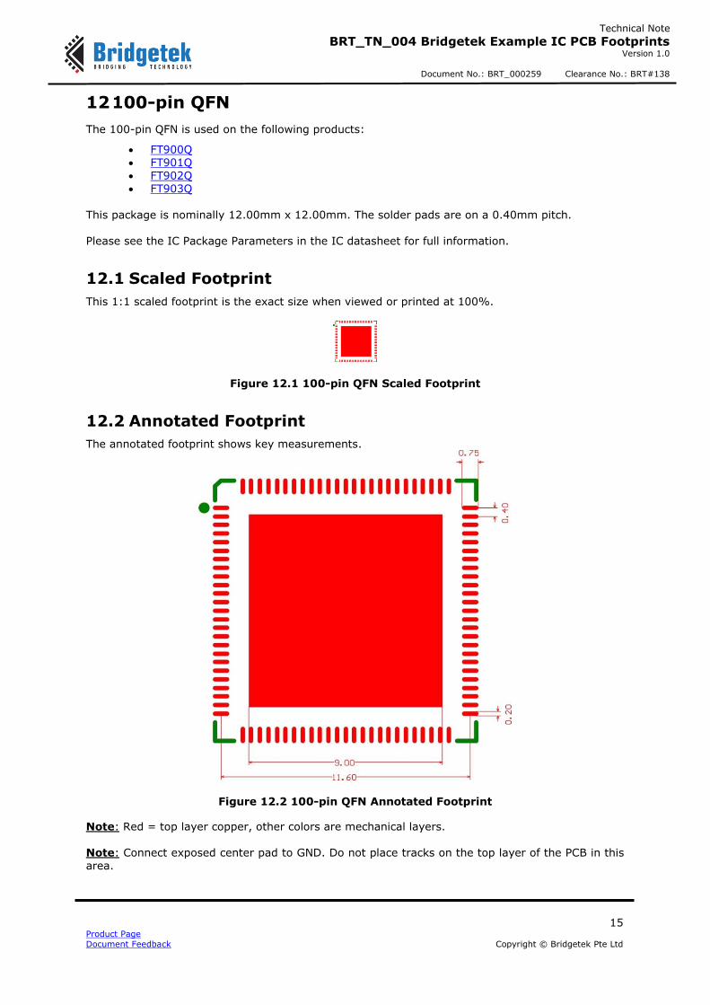
12 100-pin QFN
The 100-pin QFN is used on the following products:
FT900Q FT901Q FT902Q FT903Q
This package is nominally 12.00mm x 12.00mm. The solder pads are on a 0.40mm pitch. Please see the IC Package Parameters in the IC datasheet for full information.
12.1 Scaled Footprint
This 1:1 scaled footprint is the exact size when viewed or printed at 100%.
Figure 12.1 100-pin QFN Scaled Footprint
12.2 Annotated Footprint
The annotated footprint shows key measurements.
Figure 12.2 100-pin QFN Annotated Footprint
Note: Red = top layer copper, other colors are mechanical layers. Note: Connect exposed center pad to GND. Do not place tracks on the top layer of the PCB in this area.

16 Product Page
Document Feedback Copyright © Bridgetek Pte Ltd
Technical Note
BRT_TN_004 Bridgetek Example IC PCB Footprints Version 1.0
Document No.: BRT_000259 Clearance No.: BRT#138
13 Contact Information
Head Quarters – Singapore Branch Office – Taipei, Taiwan Bridgetek Pte Ltd 178 Paya Lebar Road, #07-03 Singapore 409030 Tel: +65 6547 4827 Fax: +65 6841 6071
Bridgetek Pte Ltd, Taiwan Branch 2 Floor, No. 516, Sec. 1, Nei Hu Road, Nei Hu District Taipei 114 Taiwan, R.O.C. Tel: +886 (2) 8797 1330 Fax: +886 (2) 8751 9737
E-mail (Sales) [email protected] E-mail (Sales) [email protected] E-mail (Support) [email protected] E-mail (Support) [email protected]
Branch Office - Glasgow, United Kingdom Branch Office – Vietnam Bridgetek Pte. Ltd. Unit 1, 2 Seaward Place, Centurion Business Park Glasgow G41 1HH United Kingdom Tel: +44 (0) 141 429 2777 Fax: +44 (0) 141 429 2758
Bridgetek VietNam Company Limited Lutaco Tower Building, 5th Floor, 173A Nguyen Van Troi, Ward 11, Phu Nhuan District, Ho Chi Minh City, Vietnam Tel : 08 38453222 Fax : 08 38455222
E-mail (Sales) [email protected] E-mail (Sales) [email protected] E-mail (Support) [email protected] E-mail (Support) [email protected]
Web Site
http://brtchip.com/
Distributor and Sales Representatives
Please visit the Sales Network page of the Bridgetek Web site for the contact details of our distributor(s) and
sales representative(s) in your country.
System and equipment manufacturers and designers are responsible to ensure that their systems, and any Bridgetek Pte Ltd
(BRTChip) devices incorporated in their systems, meet all applicable safety, regulatory and system-level performance
requirements. All application-related information in this document (including application descriptions, suggested Bridgetek
devices and other materials) is provided for reference only. While Bridgetek has taken care to assure it is accurate, this
information is subject to customer confirmation, and Bridgetek disclaims all liability for system designs and for any applications
assistance provided by Bridgetek. Use of Bridgetek devices in life support and/or safety applications is entirely at the user ’s
risk, and the user agrees to defend, indemnify and hold harmless Bridgetek from any and all damages, claims, suits or expense
resulting from such use. This document is subject to change without notice. No freedom to use patents or other intellectual
property rights is implied by the publication of this document. Neither the whole nor any part of the information contained in,
or the product described in this document, may be adapted or reproduced in any material or electronic form without the prior
written consent of the copyright holder. Bridgetek Pte Ltd, 178 Paya Lebar Road, #07-03, Singapore 409030. Singapore
Registered Company Number: 201542387H.
17 Product Page
Document Feedback Copyright © Bridgetek Pte Ltd
Technical Note
BRT_TN_004 Bridgetek Example IC PCB Footprints Version 1.0
Document No.: BRT_000259 Clearance No.: BRT#138
Appendix A– References
Document References
FT80x http://brtchip.com/i-ft80x/
FT81x http://brtchip.com/ft81x/
BT81x http://brtchip.com/bt81x/
FT90x http://brtchip.com/ft900/
FT93x http://brtchip.com/ft93x/
Altium
Acronyms and Abbreviations
Terms Description
IC Integrated Circuit
LQFP Low Profile Quad Flat Package
PCB Printed Circuit Board
QFN Quad Flat No-Leads Package
VQFN / WQFN Very Thin Quad Flat No-Lead Package
18 Product Page
Document Feedback Copyright © Bridgetek Pte Ltd
Technical Note
BRT_TN_004 Bridgetek Example IC PCB Footprints Version 1.0
Document No.: BRT_000259 Clearance No.: BRT#138
Appendix B – List of Tables & Figures
List of Tables
Table 1.1 Unavailable Footprints ..................................................................................................... 4
Table 3.1 QFP Packages ................................................................................................................. 6
Table 3.2 QFN Packages ................................................................................................................ 6
List of Figures
Figure 2.1 QFP Packages ................................................................................................................ 5
Figure 2.2 QFN Packages ............................................................................................................... 5
Figure 4.1 48-pin VQFN (7mm x 7mm) Scaled Footprint .................................................................... 7
Figure 4.2 48-pin VQFN (7mm x 7mm) Annotated Footprint ............................................................... 7
Figure 5.1 48-pin QFN (7mm x 7mm) Scaled Footprint ...................................................................... 8
Figure 5.2 48-pin QFN (7mm x 7mm) Annotated Footprint ................................................................. 8
Figure 6.1 56-pin VQFN (8mm x 8mm) Scaled Footprint .................................................................... 9
Figure 6.2 56-pin VQFN (8mm x 8mm) Annotated Footprint ............................................................... 9
Figure 7.1 64-pin VQFN (9mm x 9mm) Scaled Footprint .................................................................. 10
Figure 7.2 64-pin VQFN (9mm x 9mm) Annotated Footprint ............................................................. 10
Figure 8.1 68-pin QFN (8mm x 8mm) Scaled Footprint .................................................................... 11
Figure 8.2 68-pin QFN (8mm x 8mm) Annotated Footprint ............................................................... 11
Figure 9.1 76-pin QFN Scaled Footprint.......................................................................................... 12
Figure 9.2 76-pin QFN Annotated Footprint .................................................................................... 12
Figure 10.1 80-pin LQFP Scaled Footprint ....................................................................................... 13
Figure 10.2 80-pin LQFP Annotated Footprint ................................................................................. 13
Figure 11.1 100-pin LQFP Scaled Footprint ..................................................................................... 14
Figure 11.2 100-pin LQFP Annotated Footprint ................................................................................ 14
Figure 12.1 100-pin QFN Scaled Footprint ...................................................................................... 15
Figure 12.2 100-pin QFN Annotated Footprint ................................................................................. 15

19 Product Page
Document Feedback Copyright © Bridgetek Pte Ltd
Technical Note
BRT_TN_004 Bridgetek Example IC PCB Footprints Version 1.0
Document No.: BRT_000259 Clearance No.: BRT#138
Appendix C– Revision History
Document Title: Bridgetek Example IC PCB Footprints
Document Reference No.: BRT_000259
Clearance No.: BRT#138
Product Page: http://brtchip.com/
Document Feedback: Send Feedback
Revision Changes Date
1.0 Initial Release 2019-06-14