Embed Size (px)
Citation preview

COIL
SystemLoad
bq51025
OUT
SCL
AD
AD-EN
WPG
C4
SDA
C1
C2
CBOOT1
AC1
AC2
COIL
BOOT1RECT
C3
NTC
TS/CTRL
CLAMP1CCLAMP1
CCOMM1
COMM1
HOST
PGNDILIM
RFOD
FOD
R1
PD_DET
PMODE
BOOT2CBOOT2
COMM2CCOMM2
CLAMP2CCLAMP2
VO_REG
R6
R7
TMEMC5
CM_ILIM
R9
R8
VIREG
RECT
RMEM
Output Power (W)
Effi
cien
cy
0 1 2 3 4 5 6 7 8 9 100
10%
20%
30%
40%
50%
60%
70%
80%
90%
100%
D001
VOUT = 10V VOUT = 7V VOUT = 5V
Product
Folder
Sample &Buy
Technical
Documents
Tools &
Software
Support &Community
bq51025SLUSBX7B –SEPTEMBER 2014–REVISED MARCH 2015
bq51025 WPC v1.1 Compliant Single Chip Wireless Power ReceiverWith Proprietary 10-W Power Delivery
1 Features 3 DescriptionThe bq51025 device is a fully-contained wireless
1• Robust 10-W Receiver Solution Using Proprietarypower receiver capable of operating in the WirelessProtocol With TI's 10-W bq500215 TransmitterPower Consortium (WPC) Qi protocol, which allows a
– Post-Regulation LDO to Protect External wireless power system to deliver 5 W to the systemCharger Input from Rectifier Output Transients; with Qi inductive transmitters and up to 10 W whenInductorless Solution for Lowest Height operating with the bq500215 primary-side controller.
The bq51025 device provides a single device power– Adjustable Output Voltage (4.5 to 10 V) forconversion (rectification and regulation) as well as theCoil and Thermal Optimizationdigital control and communication as per WPC v1.1– Supports 2S Battery Configuration (Non-WPC specification. With market-leading 84% system
compliant) efficiency and adjustable output voltage, the bq51025– Fully Synchronous Rectifier With 96% device allows for unparalleled system optimization.
With a maximum output voltage of 10 V, the bq51025Efficiencyoffers a flexible solution that offers a wireless power– 97% Efficient Post Regulatorsolution for 2S battery application and allows optimal
– 84% System Efficiency at 10 W thermal performance of the system. The I2C interface• WPC v1.1 Compliant Communication and Control allows system designers to implement new features
such as aligning a receiver on the transmitter surfacefor Compatibility With Current TX Solutionsor detecting foreign objects on the receiver. The• Patented Transmitter Pad Detect Functionbq51025 device complies with the WPC v1.1Improves User Experience communication protocol making it compatible with all
• Power Signal Frequency Measurement Allows WPC transmitter solutions. The receiver allows forHost to Determine Optimal Placement on TX synchronous rectification, regulation and control, andSurface communication to all exist in a market-leading form
factor, efficiency, and solution size.• I2C Communication With Host
Device Information(1)2 ApplicationsPART NUMBER PACKAGE BODY SIZE (NOM)
• Smart Phones, Tablets, and Headsetsbq51025 DSBGA (42) 3.60 mm × 2.89 mm
• Point-of-Sale Devices(1) For all available packages, see the orderable addendum at
• 2S Battery Applications the end of the data sheet.• Power Banks• Other Portable Devices
4 Simplified Schematic
bq51025 System Efficiency With bq500215 TXController
1
An IMPORTANT NOTICE at the end of this data sheet addresses availability, warranty, changes, use in safety-critical applications,intellectual property matters and other important disclaimers. PRODUCTION DATA.

bq51025SLUSBX7B –SEPTEMBER 2014–REVISED MARCH 2015 www.ti.com
Table of Contents9.2 Functional Block Diagram ....................................... 111 Features .................................................................. 19.3 Feature Description................................................. 122 Applications ........................................................... 19.4 Device Functional Modes........................................ 183 Description ............................................................. 19.5 Register Maps ......................................................... 214 Simplified Schematic............................................. 1
10 Application and Implementation........................ 275 Revision History..................................................... 210.1 Application Information.......................................... 276 Device Comparison Table ..................................... 310.2 Typical Applications .............................................. 277 Pin Configuration and Functions ......................... 3 11 Power Supply Recommendations ..................... 398 Specifications......................................................... 5 12 Layout................................................................... 408.1 Absolute Maximum Ratings ...................................... 512.1 Layout Guidelines ................................................. 408.2 ESD Ratings.............................................................. 512.2 Layout Example .................................................... 408.3 Recommended Operating Conditions....................... 5
13 Device and Documentation Support ................. 418.4 Thermal Information .................................................. 513.1 Trademarks ........................................................... 418.5 Electrical Characteristics........................................... 613.2 Electrostatic Discharge Caution............................ 418.6 Typical Characteristics .............................................. 813.3 Glossary ................................................................ 419 Detailed Description .............................................. 9
14 Mechanical, Packaging, and Orderable9.1 Overview ................................................................... 9 Information ........................................................... 41
5 Revision HistoryNOTE: Page numbers for previous revisions may differ from page numbers in the current version.
Changes from Revision A (September 2014) to Revision B Page
• Updated Features and Description to include 2S support ..................................................................................................... 1• Added 2S Battery Application to Applications ....................................................................................................................... 1• Corrected RILIM threshold for EPT 0x02 to match Electrical Characteristics ........................................................................ 15• Corrected section numbering for TMEM ............................................................................................................................. 29• Added design example section for Standalone 10-V Power Supply for 2S Charging System............................................. 35
Changes from Original (September 2014) to Revision A Page
• Updated device status from product preview to production .................................................................................................. 1
2 Submit Documentation Feedback Copyright © 2014–2015, Texas Instruments Incorporated
Product Folder Links: bq51025
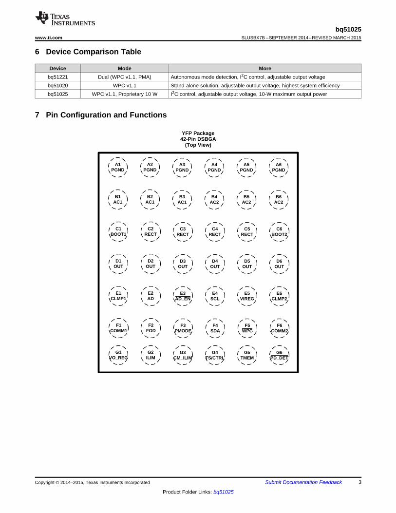
A1PGND
A2PGND
A3PGND
A4PGND
A5PGND
A6PGND
B1AC1
B2AC1
B3AC1
B4AC2
B5AC2
B6AC2
C1BOOT1
C2RECT
C3RECT
C4RECT
C5RECT
C6BOOT2
D1OUT
D2OUT
D3OUT
D4OUT
D5OUT
D6OUT
E1CLMP1
E2AD
E3AD_EN
E4SCL
E5VIREG
E6CLMP2
F1COMM1
F2FOD
F3PMODE
F4SDA
F5WPG
F6COMM2
G1VO_REG
G2ILIM
G3CM_ILIM
G4TS/CTRL
G5TMEM
G6PD_DET
bq51025www.ti.com SLUSBX7B –SEPTEMBER 2014–REVISED MARCH 2015
6 Device Comparison Table
Device Mode Morebq51221 Dual (WPC v1.1, PMA) Autonomous mode detection, I2C control, adjustable output voltagebq51020 WPC v1.1 Stand-alone solution, adjustable output voltage, highest system efficiencybq51025 WPC v1.1, Proprietary 10 W I2C control, adjustable output voltage, 10-W maximum output power
7 Pin Configuration and Functions
YFP Package42-Pin DSBGA
(Top View)
Copyright © 2014–2015, Texas Instruments Incorporated Submit Documentation Feedback 3
Product Folder Links: bq51025

bq51025SLUSBX7B –SEPTEMBER 2014–REVISED MARCH 2015 www.ti.com
Pin FunctionsPIN
TYPE DESCRIPTIONNAME NO.
B1AC1 B2 I
B3AC input power from receiver resonant tank
B4AC2 B5 I
B6AD E2 I Adapter sense pinAD-EN E3 O Push-pull driver for dual PFET circuit that can pass AD input to the OUT pin; used for adapter MUX controlBOOT1 C1 O
Bootstrap capacitors for driving the high-side FETs of the synchronous rectifierBOOT2 C6 OCLAMP1 E1 O
Open-drain FETs used to clamp the secondary voltage by providing low impedance across secondaryCLAMP2 E6 OCOMM1 F1 O
Open-drain FETs used to communicate with primary by varying reflected impedanceCOMM2 F6 OCM_ILIM G3 I Enables communication current limit when pulled low or left floating.FOD F2 I Input that is used for scaling the received power messageILIM G2 I/O Output current or overcurrent level programming pin
D1D2D3
OUT O Output pin, used to deliver power to the loadD4D5D6
PD_DET G6 O Open-drain output that allows user to sense when receiver is on transmitterA1A2A3
PGND — Power and logic groundA4A5A6C2C3
RECT O Filter capacitor for the internal synchronous rectifierC4C5
SCL E4 ISCL and SDA are used for I2C communication. Connect to ground if not needed.
SDA F4 I/OIndicates receiver mode of operation: Low = Proprietary 10-W mode, High = Low-power mode. Gate drivePMODE F3 O output for external current limit switch. Connect 5-MΩ resistor to ground. Leave floating if unused.TMEM allows the capacitor to be connected to GND so energy from transmitter ping can be stored to retainTMEM G5 O memory of state.Temperature sense. Can be pulled high to send end power transfer (EPT) – charge complete to TX. Can beTS/CTRL G4 I pulled low to send EPT – over temperature
VO_REG G1 I Sets the regulation voltage for output. Default value is 0.5 V.VIREG E5 I Rectifier voltage feedbackWPG F5 O Open-drain output that allows user to sense when power is transferred to load
4 Submit Documentation Feedback Copyright © 2014–2015, Texas Instruments Incorporated
Product Folder Links: bq51025
bq51025www.ti.com SLUSBX7B –SEPTEMBER 2014–REVISED MARCH 2015
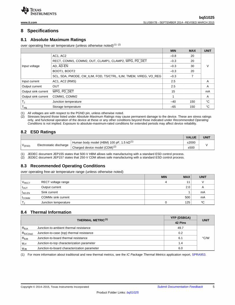
8 Specifications
8.1 Absolute Maximum Ratingsover operating free-air temperature (unless otherwise noted) (1) (2)
MIN MAX UNITAC1, AC2 –0.8 20RECT, COMM1, COMM2, OUT, CLAMP1, CLAMP2, WPG, PD_DET –0.3 20
Input voltage AD, AD-EN –0.3 30 VBOOT1, BOOT2 –0.3 20SCL, SDA, PMODE, CM_ILIM, FOD, TS/CTRL, ILIM, TMEM, VIREG, VO_REG –0.3 7
Input current AC1, AC2 (RMS) 2.5 AOutput current OUT 2.5 AOutput sink current WPG, PD_DET 15 mAOutput sink current COMM1, COMM2 1 ATJ Junction temperature –40 150 °CTstg Storage temperature –65 150 °C
(1) All voltages are with respect to the PGND pin, unless otherwise noted.(2) Stresses beyond those listed under Absolute Maximum Ratings may cause permanent damage to the device. These are stress ratings
only, and functional operation of the device at these or any other conditions beyond those indicated under Recommended OperatingConditions is not implied. Exposure to absolute-maximum-rated conditions for extended periods may affect device reliability.
8.2 ESD RatingsVALUE UNIT
Human body model (HBM) 100 pF, 1.5 kΩ (1) ±2000V(ESD) Electrostatic discharge V
Charged device model (CDM) (2) ±500
(1) JEDEC document JEP155 states that 500-V HBM allows safe manufacturing with a standard ESD control process.(2) JEDEC document JEP157 states that 250-V CDM allows safe manufacturing with a standard ESD control process.
8.3 Recommended Operating Conditionsover operating free-air temperature range (unless otherwise noted)
MIN MAX UNITVRECT RECT voltage range 4 11 VIOUT Output current 2.0 AIAD-EN Sink current 1 mAICOMM COMMx sink current 500 mATJ Junction temperature 0 125 ºC
8.4 Thermal InformationYFP (DSBGA)
THERMAL METRIC (1) UNIT42 Pins
RθJA Junction-to-ambient thermal resistance 49.7RθJC(top) Junction-to-case (top) thermal resistance 0.2RθJB Junction-to-board thermal resistance 6.1 °C/WψJT Junction-to-top characterization parameter 1.4ψJB Junction-to-board characterization parameter 6.0
(1) For more information about traditional and new thermal metrics, see the IC Package Thermal Metrics application report, SPRA953.
Copyright © 2014–2015, Texas Instruments Incorporated Submit Documentation Feedback 5
Product Folder Links: bq51025

bq51025SLUSBX7B –SEPTEMBER 2014–REVISED MARCH 2015 www.ti.com
8.5 Electrical Characteristicsover operating free-air temperature range (unless otherwise noted) , ILOAD = IOUT
PARAMETER TEST CONDITIONS MIN TYP MAX UNITVUVLO Undervoltage lockout VRECT: 0 to 3 V 2.8 2.9 VVHYS-UVLO Hysteresis on UVLO VRECT: 3 to 2 V 393 mVVRECT-OVP Input overvoltage threshold VRECT: 5 to 16 V 14.6 15.1 15.6 VVHYS-OVP Hysteresis on OVP VRECT: 16 to 5 V 1.5 V
Voltage at RECT pin set by Lower of VOUT +VRECT(REG) VOUT + 0.120 Vcommunication with primary 0.2 or 11.0VRECT(TRACK) VRECT regulation above VOUT VILIM = 1.2 V 140 mV
ILOAD hysteresis for dynamicILOAD-HYS ILOAD falling 4%VRECT thresholds as a % of IILIM
Rectifier undervoltageVRECT-DPM protection, restricts IOUT at 3 3.1 3.2 V
VRECT-DPM
Rectifier reverse voltage VRECT-REV = VOUT – VRECT,VRECT-REV protection with a supply at the 8.8 9.2 VVOUT = 10 VoutputQUIESCENT CURRENT
Quiescent current at the outputIOUT(standby) when wireless power is VOUT ≤ 5 V, 0°C ≤ TJ ≤ 85°C 20 35 µA
disabledILIM SHORT CIRCUIT
Highest value of RILIM resistor RILIM: 200 to 50 Ω. IOUT latchesRILIM-SHORT considered a fault (short). 215 230 Ωoff, cycle power to resetMonitored for IOUT > 100 mADeglitch time transition fromtDGL-Short 1 msILIM short to IOUT disableILIM-SHORT,OK enables the ILIM
ILIM_SC short comparator when IOUT is ILOAD: 0 to 200 mA 110 125 140 mAgreater than this value
ILIM-SHORT,OK Hysteresis for ILIM-SHORT,OK ILOAD: 200 to 0 mA 20 mAHYSTERESIS comparator
Maximum ILOAD that can beIOUT-CL Maximum output current limit delivered for 1 ms when ILIM is 3.7 A
shortedOUTPUT
ILOAD = 2000 mA, VO_REG resistor 0.4968 0.5019 0.5077divider ratio = 9:1ILOAD = 1 mA, VO_REG resistor 0.4971 0.5017 0.5079divider ratio = 9:1
VO_REG Feedback voltage set point VILOAD = 1000 mA, VO_REG resistor 0.4977 0.5027 0.5091divider ratio = 19:1ILOAD = 1 mA, VO_REG resistor 0.4978 0.5029 0.5098divider ratio = 19:1
Current programming factor for RILIM = KILIM / IILIM, where IILIM isKILIM hardware short circuit the hardware current limit 842 AΩ
protection IOUT = 900 mACurrent limit programmingIOUT_RANGE 2300 mArange
IOUT ≥ 400 mA IOUT – 50Output current limit duringICOMM 100 mA ≤ IOUT < 400 mA IOUT + 50 mAcommunication
IOUT < 100 mA 200Hold off time for the
tHOLD-OFF communication current limit 1 sduring startup
6 Submit Documentation Feedback Copyright © 2014–2015, Texas Instruments Incorporated
Product Folder Links: bq51025

bq51025www.ti.com SLUSBX7B –SEPTEMBER 2014–REVISED MARCH 2015
Electrical Characteristics (continued)over operating free-air temperature range (unless otherwise noted) , ILOAD = IOUT
PARAMETER TEST CONDITIONS MIN TYP MAX UNITTS/CTRL
ITS-Bias < 100 µA andcommunication is activeVTS-Bias TS bias voltage (internal) 1.8 V(periodically driven, see tTS/CTRL-Meas)
VCTRL-HI CTRL pin threshold for a high VTS/CTRL: 50 to 150 mV 90 105 120 mVTime period of TS/CTRL TS bias voltage is only drivenTTS/CTRL-Meas measurements, when TS is 1700 mswhen power packets are sentbeing driven
VTS-HOT Voltage at TS pin when device 0.38 Vshuts down
THERMAL PROTECTIONTJ(OFF) Thermal shutdown temperature 155 °CTJ(OFF-HYS) Thermal shutdown hysteresis 20 °COUTPUT LOGIC LEVELS ON WPGVOL Open-drain WPG pin ISINK = 5 mA 550 mV
WPG leakage current whenIOFF,STAT VWPG = 20 V 1 µAdisabledCOMM PINRDS-ON(COMM) COMM1 and COMM2 VRECT = 2.6 V 1 Ω
Signaling frequency on COMMxƒCOMM 2.00 Kb/spin for WPCIOFF,COMM COMMx pin leakage current VCOMM1 = 20 V, VCOMM2 = 20 V 1 µACLAMP PINRDS- CLAMP1 and CLAMP2 0.5 ΩON(CLAMP)
ADAPTER ENABLEVAD-EN VAD rising threshold voltage VAD 0 V to 5 V 3.5 3.6 3.8 VVAD-EN-HYS VAD-EN hysteresis VAD 5 V to 0 V 450 mVIAD Input leakage current VRECT = 0 V, VAD = 5 V 50 μA
Pullup resistance from AD-ENRAD_EN-OUT to OUT when adapter mode is VAD = 0 V, VOUT = 5 V 230 350 Ω
disabled and VOUT > VAD
Voltage difference between VAD VAD = 5 V, 0°C ≤ TJ ≤ 85°C 4 4.5 5 VVAD_EN-ON and VAD-EN when adapter mode
VAD = 9 V, 0°C ≤ TJ ≤ 85°C 3 6 7 Vis enabledSYNCHRONOUS RECTIFIER
IOUT at which the synchronousISYNC-EN rectifier enters half IOUT: 200 to 0 mA 100 mA
synchronous modeHysteresis for IOUT,RECT-EN (full-ISYNC-EN-HYST IOUT: 0 to 200 mA 40 mAsynchronous mode enabled)High-side diode drop when the IAC-VRECT = 250 mA, andVHS-DIODE rectifier is in half synchronous 0.7 VTJ = 25°Cmode
I2CVIL Input low threshold level SDA V(PULLUP) = 1.8 V, SDA 0.4 VVIH Input high threshold level SDA V(PULLUP) = 1.8 V, SDA 1.4 VVIL Input low threshold level SCL V(PULLUP) = 1.8 V, SCL 0.4 VVIH Input high threshold level SCL V(PULLUP) = 1.8 V, SCL 1.4 V
I2C speed Typical 100 kHz
Copyright © 2014–2015, Texas Instruments Incorporated Submit Documentation Feedback 7
Product Folder Links: bq51025

I2C Code
VO
_RE
G (
V)
0 10.45
0.455
0.46
0.465
0.47
0.475
0.48
0.485
0.49
0.495
0.5
0.505
D006
IOUT = 1mAIOUT = 1A
Temperature (qC)
VU
VLO
(V
)
-40 -20 0 20 40 60 80 100 1202.785
2.7875
2.79
2.7925
2.795
2.7975
2.8
2.8025
2.805
2.8075
2.81
2.8125
2.815
D004 I2C Code
VO
_RE
G (
V)
0 1 2 3 4 5 6 70.45
0.5
0.55
0.6
0.65
0.7
0.75
0.8
0.85
D005
IOUT = 1mAIOUT = 1A
IOUT (A)
VO
_RE
G (
V
0 0.2 0.4 0.6 0.8 1 1.2 1.4 1.6 1.8 20.498
0.499
0.5
0.501
0.502
0.503
0.504
0.505
0.506
D002 ILOAD (mA)
KIL
IM (
A:
)
0 200 400 600 800 1000 1200 1400 1600 1800 2000830
832.5
835
837.5
840
842.5
845
847.5
850
852.5
855
D003
bq51025SLUSBX7B –SEPTEMBER 2014–REVISED MARCH 2015 www.ti.com
8.6 Typical Characteristics
Temperature =25°C
Figure 2. KILIM as a Function of Load CurrentFigure 1. Output Regulation as a Function of Load
Figure 3. UVLO as a Function of Junction Temperature Figure 4. VO_REG by Different I2C Codes, Resistor DividerRatio = 9:1
Figure 5. VO_REG by Different I2C Codes, Resistor Divider Ratio = 19:1
8 Submit Documentation Feedback Copyright © 2014–2015, Texas Instruments Incorporated
Product Folder Links: bq51025

bq51025www.ti.com SLUSBX7B –SEPTEMBER 2014–REVISED MARCH 2015
9 Detailed Description
9.1 OverviewWPC-based wireless power systems consist of a charging pad (primary, transmitter) and the secondary-sideequipment (receiver). The coils in the charging pad and secondary equipment magnetically couple to each otherwhen the receiver is placed on the transmitter. Power is transferred from the primary to the secondary bytransformer action between the coils. The receiver can achieve control over the amount of power transferred bygetting the transmitter to change the field strength by changing the frequency, duty cycle, or voltage railenergizing the primary coil.
The receiver equipment communicates with the primary by modulating the load seen by the primary. This loadmodulation results in a change in the primary coil current or primary coil voltage, or both, which is measured anddemodulated by the transmitter.
In WPC, the system communication is digital (packets that are transferred from the secondary to the primary).Differential biphase encoding is used for the packets. The bit rate is 2 kb/s. Various types of communicationpackets are defined. These include identification and authentication packets, error packets, control packets,power usage packets, and end power transfer packets, among others.
The bq51025 incorporates a two-way proprietary authentication with the bq500215 primary controller that allowsoptimal power transfer and system performance up to 10-W output power while still complying with WPC v1.1specifications.
Figure 6. Wireless Power System Indicating the Functional Integration of the bq51025
The bq51025 device integrates fully-compliant WPC v1.1 communication protocol to streamline the wirelesspower receiver designs (no extra software development required). Other unique algorithms such as DynamicRectifier Control are integrated to provide best-in-class system efficiency while keeping the smallest solution sizeof the industry.
Copyright © 2014–2015, Texas Instruments Incorporated Submit Documentation Feedback 9
Product Folder Links: bq51025

bq51025SLUSBX7B –SEPTEMBER 2014–REVISED MARCH 2015 www.ti.com
Overview (continued)As a WPC system, when the receiver (shown in Figure 6) is placed on the charging pad, the secondary coilcouples to the magnetic flux generated by the coil in the transmitter, which consequently induces a voltage in thesecondary coil. The internal synchronous rectifier feeds this voltage to the RECT pin, which in turn feeds theLDO which feeds the output.
The bq51025 device identifies and authenticates itself to the primary using the COMMx pins, switching on and offthe COMM FETs, and hence, switching in and out COMM capacitors. If the authentication is successful, theprimary remains powered-up. Using a proprietary authentication protocol, the bq51025 determines if the 10-Wbq500215 primary controller is powering the device, in which case the bq51025 device allows operation up to 10-W. If the bq51025 determines that a standard WPC-compliant transmitter is powering it, it allows operation up to5-W. The bq51025 device measures the voltage at the RECT pin, calculates the difference between the actualvoltage and the desired voltage VRECT(REG) and sends back error packets to the transmitter. This process goes onuntil the input voltage settles at VRECT(REG) MAX. During a load change, the dynamic rectifier algorithm sets thetarget voltage between VRECT(REG) MAX and VRECT(REG) MIN, as shown in Table 1. This algorithm enhances thetransient response of the power supply.
After the voltage at the RECT pin is at the desired value, the pass FET is enabled. The voltage control loopensures that the output voltage is maintained at VOUT(REG), powering the downstream charger. The bq51025device meanwhile continues to monitor the input voltage, and keeps sending control error packets (CEP) to theprimary, on average, every 250 ms. If a large transient occurs, the feedback to the primary speeds up to 32-mscommunication periods to converge on an operating point in less time.
10 Submit Documentation Feedback Copyright © 2014–2015, Texas Instruments Incorporated
Product Folder Links: bq51025

ILIM
+_
+_
+_
+_
OUT
AD
+_
VREFAD,OVP
VREFAD,UVLO
+_
/AD-EN
FOD
TS/CTRL
ADC
VREF,IABS
VIN,DPM
VOUT,REG
VOUT,FB
VILIM
VREF,ILIM
VIABS,FB
VIN,FB
VBG,REF
VIN,FB
VOUT,FB
VILIM
VIABS,FB
VIC,TEMP
VIABS,REF
Sync Rectifier Control
AC1AC2
BOOT1
BOOT2
RECT
Digital Control
DATA_OUT
COMM1
COMM2
+_
VRECTVOVP,REF
OVP
PGND
,
CLAMP1
CLAMP2
SCL
SDA
/WPG
VFOD
VFOD
VIREG
VOREG
PMODE
50uA
PMODE
CM_ILIM
TMEM
SCL
SDA
/PD_DET
TS
5W_MODE
bq51025www.ti.com SLUSBX7B –SEPTEMBER 2014–REVISED MARCH 2015
9.2 Functional Block Diagram
Copyright © 2014–2015, Texas Instruments Incorporated Submit Documentation Feedback 11
Product Folder Links: bq51025

DIS RECT OUT OUTP V V I
bq51025SLUSBX7B –SEPTEMBER 2014–REVISED MARCH 2015 www.ti.com
9.3 Feature Description
9.3.1 Dynamic Rectifier ControlThe Dynamic Rectifier Control algorithm offers the end-system designer optimal transient response for a givenmaximum output current setting. This is achieved by providing enough voltage headroom across the internalregulator (LDO) at light loads in order to maintain regulation during a load transient. The WPC system has arelatively slow global feedback loop where it can take up to 150 ms to converge on a new rectifier voltage target.Therefore, a transient response depends on the loosely-coupled transformer's output-impedance profile. TheDynamic Rectifier Control allows for a 1.5-V change in rectified voltage before the transient response is observedat the output of the internal regulator (output of the bq51025 device). A 1-A application allows up to a 2-Ω outputimpedance. Figure 13 shows the Dynamic Rectifier Control behavior during active power transfer.
9.3.2 Dynamic Power ScalingThe Dynamic Power Scaling feature allows for the loss characteristics of the bq51025 device to be scaled basedon the maximum expected output power in the end application. This effectively optimizes the efficiency for eachapplication. This feature is achieved by scaling the loss of the internal LDO based on a percentage of themaximum output current. Note that the maximum output current is set by the KILIM term and the RILIM resistance(where RILIM = KILIM / IILIM). The flow diagram in Figure 13 shows how the rectifier is dynamically controlled(Dynamic Rectifier Control) based on the voltage level at the ILIM pin (VILIM). This voltage represents a fixedpercentage of the IILIM setting. Table 1 summarizes how the rectifier behavior is dynamically adjusted based ontwo different RILIM settings. Table 1 is shown for IMAX, which is the maximum operating output current and istypically lower than IILIM (about 20% lower). See RILIM Calculations for more details on how to set IILIM.
Table 1. Dynamic Rectifier Regulation (1)
Low Power (5-W) Low Power (5-W) Proprietary 10-WOutput Current Output Current Mode Mode Mode
Percentage Percentage RILIM = 700 Ω RILIM = 700 Ω RILIM = 495 Ω VRECT(2)
(Low-Power Mode) (Proprietary Mode) IILIM = 0.6 A IILIM = 1.2 A IILIM = 1.7 A(IMAX = 0.5 A) (IMAX = 1 A) (IMAX = 1.4 A)
0 to 10% 0 to 5% 0 to 0.05 A 0 to 0.05 A 0 to 0.070 A VOUT + 2.010 to 20% 5 to 10% 0.05 to 0.1 A 0.05 to 0.1 A 0.070 to 0.14 A VOUT + 1.620 to 40% 10 to 20% 0.1 to 0.2 A 0.1 to 0.2 A 0.14 to 0.28 A VOUT + 0.6
>40% >20% >0.2 A >0.2 A >0.28 A VOUT + 0.12
(1) ROS = Open. The relation between VILIM and ILIM has some dependency on the ROS value.(2) VRECT is regulated to a maximum of 11 V.
Table 1 shows the shift in the Dynamic Rectifier Control behavior based on the two different RILIM settings. Withthe rectifier voltage (VRECT) as the input to the internal LDO, this adjustment in the Dynamic Rectifier Controlthresholds dynamically adjusts the power dissipation across the LDO where,
(1)
Figure 22 shows how the Dynamic Power Scaling feature reduces the VRECT with increased load, allowing thepost-regulation LDO to have maximum headroom at low load conditions for better load transient performanceand minimal power dissipation at high loads. Note that this feature balances efficiency with optimal systemtransient response.
9.3.3 VO_REG CalculationsThe bq51025 device allows the designer to set the output voltage by setting a feedback resistor divider networkfrom the OUT pin to the VO_REG pin, as seen in Figure 7. Select the resistor divider network so that the voltageat the VO_REG pin is 0.5 V (default setting) at the desired output voltage. The target VO_REG voltage can bechanged through I2C by changing Table 4
12 Submit Documentation Feedback Copyright © 2014–2015, Texas Instruments Incorporated
Product Folder Links: bq51025

LP-ILIM
ILIM
LP-ILIMI2
KR
u
1 ILIM FOD5 5 ± 5
ILIMILIM
ILIM
KR
I
VO 76
VO
K RR
1 K
u
VOOUT
0.5 VK
V
R6
R7
OUT
VO_REG
bq51025www.ti.com SLUSBX7B –SEPTEMBER 2014–REVISED MARCH 2015
Figure 7. VO_REG Network
Choose the desired output voltage VOUT and R6:
(2)
(3)
9.3.4 RILIM CalculationsThe bq51025 device includes a means of providing hardware overcurrent protection (IILIM) through an analogcurrent regulation loop. The hardware current limit provides an extra level of safety by clamping the maximumallowable output current (for example, current compliance). The RILIM resistor size also sets the thresholds for thedynamic rectifier levels providing efficiency tuning per each application’s maximum system current. Thecalculation for the total RILIM resistance is as follows:
(4)
(5)
The RILIM allows for the ILIM pin to reach 1.2 V when operating in proprietary mode (up to 10-W output power)when the output current is equal to IILIM. When the receiver operates in standard WPC low-power mode, the ILIMpin voltage threshold is changed from 1.2 to 0.6 V, setting the low-power mode current limit to half of that at theproprietary mode setting.
In the case where having the current limit change by a factor of two between modes is not desired, the twocurrent limit levels may be independently controlled in two ways:• By programming the IO_REG level through I2C• By changing the effective RILIM value for each mode by using an external switch controlled by the PMODE pin
To adjust the current limit for each mode through I2C, RILIM is chosen using Equation 4 where IILIM is the currentlimit for proprietary mode (that is, higher current setting). The host should first set the desired current limit valuefor low-power mode as a percentage of IILIM through the IO_REG bits and then disable the 2X current scaling bysetting the I2C_ILIM bit in Table 5 and Table 6 respectively to enable programmability. By default, IO_REG is setto the highest current setting allowed by RILIM (that is, 100% of IILIM).
If I2C control is not available, the current limit for low power and proprietary modes can be set independently byshorting a portion of the R1 resistance using an external switch as shown in Figure 8. RILIM is calculated usingEquation 4, where IILIM is the desired current limit for proprietary mode. The resistance to set the current limit inlow-power mode, RILIM_LP is calculated by Equation 6.
where IILIM_LP is the desired current limit value in low-power mode (6)
Copyright © 2014–2015, Texas Instruments Incorporated Submit Documentation Feedback 13
Product Folder Links: bq51025

1 ILIM FOD5 5 ± 5
ILIMILIM
ILIM
KR
1.1 I
u
R1_A R1_B
RFOD
ROS
RECT
PMODE
ILIM
FOD
bq51025SLUSBX7B –SEPTEMBER 2014–REVISED MARCH 2015 www.ti.com
The value for R1_A is given by RILIM_LP – RFOD. The value of R1_B is then RILIM – R1_A – RFOD. Note that with thismethod IILIM must be less than 2 × IILIM_LP
Figure 8. Current Limit Setting for bq51025 Using External Switch
When choosing IILIM, consider the following two possible operating conditions:• If the user's application requires an output current equal to or greater than the external IILIM that the circuit is
designed for (input current limit on the charger where the receiver device is tied higher than the external IILIM),ensure that the downstream charger is capable of regulating the voltage of the input into which the receiverdevice output is tied to by lowering the amount of current being drawn. This ensures that the receiver outputdoes not drop to zero. Such behavior is referred to as VIN DPM in TI chargers. Unless such behavior isenabled on the charger, the charger pulls the output of the receiver device to ground when the receiverdevice enters current regulation.
• If the user's applications are designed to extract less than the IILIM, typical designs should leave a designmargin of at least 10%, so that the voltage at ILIM pin reaches 1.2 V when 10% more than maximum currentis drawn from the output. Such a design would have input current limit on the charger lower than the externalILIM of the receiver device.
However, in both cases, the charger must be capable of regulating the current drawn from the device to allow theoutput voltage to stay at a reasonable value. This same behavior is also necessary during the WPCcommunication. The following calculations show how such a design is achieved:
(7)
where ILIM is the hardware current limit (8)
When referring to the application diagram shown in Typical Applications, RILIM is the sum of the R1 and RFODresistance (that is, the total resistance from the ILIM pin to GND). RFOD is chosen according to the application. Toobtain the tool for calculating RFOD, contact your TI representative. Use RFOD to allow the receiver implementationto comply with WPC v1.1 requirements related to received power accuracy.
9.3.5 Adapter Enable FunctionalityThe bq51025 device can also help manage the multiplexing of adapter power to the output and can shut off theTX when the adapter is plugged in and is above the VAD-EN. After the adapter is plugged in and the output turnsoff, the RX device sends an EPT to the TX. In this case, the AD_EN pins are then pulled to approximately 4 Vbelow AD, which allows the device to turn on the back-to-back PMOS connected between AD and OUT (seeFigure 32).
Both the AD and AD-EN pins are rated at 30 V, while the OUT pin is rated at 20 V. Note that it is required toconnect a back-to-back PMOS between AD and OUT so that voltage is blocked in both directions. Also, whenAD mode is enabled, no load can be pulled from the RECT pin because this could cause an internal deviceovervoltage in the bq51025 device.
14 Submit Documentation Feedback Copyright © 2014–2015, Texas Instruments Incorporated
Product Folder Links: bq51025

bq51025www.ti.com SLUSBX7B –SEPTEMBER 2014–REVISED MARCH 2015
9.3.6 Turning Off the TransmitterThe WPC v1.1 specification allows the receiver to turn off the transmitter and put the system in a low-powerstandby mode. There are two different ways to accomplish this with the bq51025 device. The EPT chargecomplete (WPC) can be sent to the TX by pulling the TS pin high (above 1.4 V). The bq51025 device will thensense this and send the appropriate signal to the TX, thus putting the TX in a low-power standby mode.
9.3.6.1 WPC v1.1 EPTThe WPC allows for a special command to terminate power transfer from the TX-termed EPT packet. The WPCv1.1 specifies the following reasons and their corresponding data field value in Table 2.
Table 2. EPT Codes in WPCReason Value Condition (1)
Unknown 0x00 AD > 3.6 VCharge complete 0x01 TS/CTRL > 1.4 V
Internal fault 0x02 TJ > 150°C or RILIM < 215 ΩOver temperature 0x03 TS < VHOT, or TS/CTRL < 100 mV (2)
Over voltage 0x04 VRECT voltage does not converge and stays higher than targetBattery failure 0x06 Not sentReconfigure 0x07 Not sentNo response 0x08 Not sent
(1) The Condition column corresponds to the case where the bq51025 device sends the WPC EPTcommand.
(2) The TS < VTS-HOT condition refers to using an external thermistor for temperature control. TheTS/CTRL <100-mV condition refers to driving the TS/CTRL pin from external GPIO.
9.3.7 Communication Current LimitCommunication current limit is a feature that allows for error-free communication to happen between the RX andTX in the WPC mode. This is done by decoupling the coil from the load transients by limiting the output currentduring communication with the TX. The communication current limit is set according to Table 3. Thecommunication current limit can be enabled by pulling CM_ILIM pin low or disabled by pulling the CM_ILIM pinhigh (>1.4 V) . An internal pulldown enables communication current limit when the CM_ILIM pin is left floating.
Table 3. Communication Current LimitIOUT Communication Current Limit
0 mA < IOUT < 100 mA None100 mA < IOUT < 400 mA IOUT + 50 mA
400 mA < IOUT < Max current IOUT – 50 mA
When the communication current limit is enabled, the amount of current that the load can draw is limited. If thecharger in the system does not have a VIN-DPM feature, the output of the receiver collapses if communicationcurrent limit is enabled. Please note that power dissipation within the device will increase during current limiting,lowering overall system efficiency. To disable communication current limit, pull CM_ILIM pin high.
9.3.8 PD_DET and TMEMPD_DET is an open-drain pin that goes low based on the voltage of the TMEM pin. When the voltage of TMEMis higher than 1.6 V, PD_DET is low. The voltage on the TMEM pin depends on capturing the energy from thedigital ping from the transmitter and storing it on the C5 capacitor in Figure 9. After the receiver sends an EPT(charge complete), the transmitter shuts down and goes into a low-power mode. However, it continues to check ifthe receiver would like to renegotiate a power transfer by periodically performing the digital ping. The energyfrom the digital ping can be stored on the TMEM pin until the next digital ping refreshes the capacitor. Thedesigner can choose a bleedoff resistor, RMEM, in parallel with C5 that sets the time constant so that the TMEMpin will fall below 1.6 V once the next ping timer expires. The duration between digital pings is indeterminate anddepends on each transmitter manufacturer.
Copyright © 2014–2015, Texas Instruments Incorporated Submit Documentation Feedback 15
Product Folder Links: bq51025

NTCHOT 1 3
NTCHOT 1 3TS HOT
NTCHOT 1 32
NTCHOT 1 3
R R R
R R RV 1.8 V
R R RR
R R R
u
u
u
20 k
NTC
VTSB
(1.8 V)
TS/CTRLR3
R2
R1
5
ping
MEMC4
tR
u
TMEMC5 RMEM
bq51025SLUSBX7B –SEPTEMBER 2014–REVISED MARCH 2015 www.ti.com
Figure 9. TMEM Configuration
Set capacitor on C5 = TMEM to 2.2 µF. Resistor RMEM across C5 can be set by understanding the durationbetween digital pings (tping). Set the resistor such that:
(9)
PD_DET typically requires a pullup resistor to an external source. A higher current through the PD_DET pin mayaffect the output regulation of the device. To improve regulation, TI recommends pullup resistor values in therange of 15 to 100 kΩ.
9.3.9 TS/CTRLThe bq51025 device includes a ratiometric external temperature sense function. The temperature sense functionhas a low ratiometric threshold which represents a hot condition. TI recommends an external temperature sensorto provide safe operating conditions for the receiver product. This pin is best used for monitoring the surface thatcan be exposed to the end user (for example, place the negative temperature coefficient (NTC) resistor closest tothe user touch point on the back cover). A resistor in series or parallel can be inserted to adjust the NTC tomatch the trip point of the device. The implementation in Figure 10 shows the series-parallel resistorimplementation for setting the threshold at which VTS-HOT is reached. When the VTS-HOT threshold is reached, thedevice will send an EPT – overtemperature signal for a WPC transmitter.
Figure 10. NTC Resistor Setup
Figure 10 shows a parallel resistor setup that can be used to adjust the trip point of VTS-HOT. After the NTC ischosen and RNTCHOT at VTS-HOT is determined from the data sheet of the NTC, use Equation 10 to calculate R1and R3. In many cases, depending on the NTC resistor, R1 or R3 can be omitted. To omit R1, set R1 to 0, and toomit R3, set R3 to 10 MΩ in the calculation.
(10)
16 Submit Documentation Feedback Copyright © 2014–2015, Texas Instruments Incorporated
Product Folder Links: bq51025

Frequency (kHz)
I2 C C
ode
(Dec
imal
)
100 105 110 115 120 125 130 135 140 145 150 155 160 165 170 175 180 185 190 195 200 205 21030
40
50
60
70
80
D014
u
0.982
ACT &RGH
bq51025www.ti.com SLUSBX7B –SEPTEMBER 2014–REVISED MARCH 2015
9.3.10 PMODE PinConnect a 5-MΩ resistor to ground in order to use PMODE to indicate the receiver mode of operation. PMODE ishigh when in low-power mode and low in proprietary mode. This pin may be used to control the gate of anNMOS switch to change the RILIM, and hence, the current limit based on the maximum power allowed by thetransmitter (10 W for bq500215, 5 W or less otherwise). This pin may be left floating if not used. and show thePMODE behavior during startup.
9.3.11 I2C CommunicationThe bq51025 device allows for I2C communication with the internal CPU. The I2C address for the device is 0x6C.In case the I2C is not used, ground SCL and SDA. See Register Maps for more information.
9.3.12 Input OvervoltageIf the input voltage suddenly increases in potential for some condition (for example, a change in position of theequipment on the charging pad), the voltage-control loop inside the bq51025 device becomes active, andprevents the output from going beyond VOUT(REG). The receiver then starts sending back error packets every 32ms until the input voltage comes back to an acceptable level, and then maintains the error communication every250 ms.
If the input voltage increases in potential beyond VRECT_OVP, the device switches off the LDO and informs theprimary to terminate power. In addition, a proprietary voltage protection circuit is activated by means of CCLAMP1and CCLAMP2 that protects the device from voltages beyond the maximum rating of the device.
9.3.13 Alignment Aid Using Frequency InformationThe bq51025 device provides the host through I2C with power signal frequency information that would enable itto determine the optimal alignment position on the charging surface of a frequency-controlled transmitter. Forthese WPC transmitters, the power signal frequency increases as the coupling between the primary andsecondary coils increases. By finding the position in the charging pad that has the highest frequency, the hostcan determine that the best possible alignment with the transmitter coil has been achieved.
The bq51025 continuously stores a measurement of the power signal frequency in I2C register 0xFB to providethe host the information it needs to determine optimal placement. The power signal frequency is given by:
where ƒAC is the power signal frequency measured at the AC pins in kHz and code is the decimal value inthe 0xFB register (11)
Figure 11 shows the expected register values across the frequency range.
Figure 11. I2C Code vs Power Signal Frequency
Copyright © 2014–2015, Texas Instruments Incorporated Submit Documentation Feedback 17
Product Folder Links: bq51025

bq51025SLUSBX7B –SEPTEMBER 2014–REVISED MARCH 2015 www.ti.com
9.4 Device Functional ModesAt startup operation, the bq51025 device must comply with proper handshaking to be granted a power contractfrom the WPC transmitter. The transmitter initiates the handshake by providing an extended digital ping afteranalog ping detects an object on the transmitter surface. If a receiver is present on the transmitter surface, thereceiver then provides the signal strength, configuration, and identification packets to the transmitter (see volume1 of the WPC specification for details on each packet). These are the first three packets sent to the transmitter.The only exception is if there is a true shutdown condition on the AD or TS/CTRL pins where the receiver shutsdown the transmitter immediately. See Table 2 for details. After the transmitter has successfully received thesignal strength, configuration, and identification packets, the receiver is granted a power contract and is thenallowed to control the operating point of the power transfer. With the use of the bq51025 device DynamicRectifier Control algorithm, the receiver informs the transmitter to adjust the rectifier voltage to approximately 8 Vprior to enabling the output supply. For startup flow diagram details, see Figure 12.
To operate in 10-W mode, the bq51025 device performs a proprietary handshaking procedure with thetransmitter. If the transmitter (bq500215) responds to the bq51025 handshake, a 10-W power contract is grantedand the bq51025 operates in 10-W mode, setting the proper output current limit and control. If there is noresponse from the transmitter, the bq51025 device defaults to 5-W mode operation.
18 Submit Documentation Feedback Copyright © 2014–2015, Texas Instruments Incorporated
Product Folder Links: bq51025

Tx Powered without Rx
Active
Signal Stength, Identification & Configuration
Received by Tx?
No
Yes
Tx Extended Digital Ping
WPC Power Contract Established. All
proceeding control is dictated by the Rx.
VRECT < 8 V?Send control error packet
to increase VRECT
Yes
No
Startup operating point established. Enable the
Rx output.
AD/TS-CTRL EPT Condition?
Send EPT packet with reason value
Yes
No
Rx Active Power Transfer
Stage
Is Transmitter bq500215?
10-W Power Contract Established. All
proceeding control is dictated by the Rx.
No Yes
bq51025www.ti.com SLUSBX7B –SEPTEMBER 2014–REVISED MARCH 2015
Device Functional Modes (continued)
Figure 12. Wireless Power Startup Flow Diagram on WPC TX
Copyright © 2014–2015, Texas Instruments Incorporated Submit Documentation Feedback 19
Product Folder Links: bq51025

Rx Shutdown conditions per the EPT
Table?
Send EPT packet with reason value
Is VILIM < 0.05 V?
VRECT target = Minimum of (VOUT + 2 V) or 11V. Send
control error packets to converge.
Yes
No
Is VILIM < 0.1 V?
VRECT target = VOUT + 1.6 V. Send control error packets
to converge.
Yes
No
Is VILIM < 0.2 V?
VRECT target = VOUT + 0.6 V. Send control error packets
to converge.
Yes
No
VRECT target = VOUT + 0.12 V. Send control error packets to
converge.
Yes
No
Rx Active Power Transfer
Stage
Tx Powered without Rx
Active
Measure Received Power and Send Value to Tx
bq51025SLUSBX7B –SEPTEMBER 2014–REVISED MARCH 2015 www.ti.com
Device Functional Modes (continued)After the startup procedure is established, the receiver enters the active-power transfer stage (considered themain loop of operation). The Dynamic Rectifier Control algorithm determines the rectifier voltage target based ona percentage of the maximum output current level setting (set by KILIM and RILIM). The receiver sends controlerror packets to converge on these targets. As the output current changes, the rectifier voltage target dynamicallychanges. As a note, the feedback loop of the WPC system is relatively slow, it can take up to 150 ms toconverge on a new rectifier voltage target. It should be understood that the instantaneous transient response ofthe system is open loop and dependent on the receiver coil output impedance at that operating point. The mainloop also determines if any conditions in Table 2 are true in order to discontinue power transfer. Figure 13 showsthe active-power transfer loop.
Figure 13. Active Power Transfer Flow Diagram on WPC TX
20 Submit Documentation Feedback Copyright © 2014–2015, Texas Instruments Incorporated
Product Folder Links: bq51025

bq51025www.ti.com SLUSBX7B –SEPTEMBER 2014–REVISED MARCH 2015
9.5 Register MapsLocations 0x01 and 0x02 can be written at any time. Locations 0xE0 to 0xFF are only functional when VRECT >VUVLO. When VRECT goes below VUVLO, locations 0xE0 to 0xFF are reset.
9.5.1 Wireless Power Supply Current Register 1
Table 4. Wireless Power Supply Current Register 1 (READ / WRITE)Memory Location: 0x01, Default State: 00000001
BIT NAME READ / WRITE FUNCTIONB7 (MSB) Read / Write Not used
B6 Read / Write Not usedB5 Read / Write Not usedB4 Read / Write Not usedB3 Read / Write Not usedB2 VOREG2 Read / Write 450, 500, 550, 600, 650, 700, 750, or 800 mV (1)
B1 VOREG1 Read / Write Changes VO_REG targetDefault value 001B0 VOREG0 Read / Write
(1) Maximum output voltage is limited to 10 V. Maximum VO_REG setting is 0.5 V when default output voltage is set to 10 V with externalresistor divider (19:1 ratio)
9.5.2 Wireless Power Supply Current Register 2
Table 5. Wireless Power Supply Current Register 2 (READ / WRITE)Memory Location: 0x02, Default State: 00000111
BIT NAME READ / WRITE FUNCTIONB7 (MSB) JEITA Read / Write Not used
B6 Read / Write Not usedB5 ITERM2 Read / WriteB4 ITERM1 Read / Write Not used.B3 ITERM0 Read / WriteB2 IOREG2 Read / Write 10%, 20%, 30%, 40%, 50%, 60%, 80%, and 100% of IILIM currentB1 IOREG1 Read / Write based on configuration
000, 001, ….111B0 IOREG0 Read / Write
9.5.3 Wireless Power Supply Current Register 3
Table 6. Wireless Power Supply Current Register 3 (READ / WRITE)Memory Location: 0xF0, Reset State: 00000000
BIT NAME READ / WRITE FUNCTIONB7 Reserved Read/WriteB6 Reserved Read / WriteB5 Reserved Read / WriteB4 Reserved Read / WriteB3 Reserved Read / WriteB2 Reserved Read / Write
Set bit to 1 to disable 2× current limit scaling between low-power andB1 I2C_ILIM Read / Write proprietary modes. Must be set to 1 to correctly adjust the current limit
for each mode through I2CB0 Reserved Read / Write
Copyright © 2014–2015, Texas Instruments Incorporated Submit Documentation Feedback 21
Product Folder Links: bq51025

bq51025SLUSBX7B –SEPTEMBER 2014–REVISED MARCH 2015 www.ti.com
9.5.4 I2C Mailbox Register
Table 7. I2C Mailbox Register (READ / WRITE)Memory Location: 0xE0, Reset State: 10000000
BIT NAME READ / WRITE FUNCTIONSet bit to 0 to send proprietary packet with header in 0xE2.CPU checks header to pick relevant payload from 0xF1 to 0xF4B7 USER_PKT_DONE Read/Write This bit will be set to 1 after the user packet with the header in register0xE2 is sent.
B6 00 = No error in sending packet01 = Error: No transmitter presentUSER_PKT_ERR Read 10 = Illegal header found: packet will not be sentB511 = Error: Not defined yet
B4 FOD Mailer Read / Write Not usedSetting this bit to 1 enables alignment aid mode where the CEP = 0 isB3 ALIGN Mailer Read / Write sent until this bit is set to 0 (or CPU reset occurs)
B2 FOD Scaler Read / Write Not used, write to 0 if register is writtenB1 Reserved Read / WriteB0 Reserved Read / Write
9.5.5 I2C Mailbox Register 2
Table 8. I2C Mailbox Register 2 (READ / WRITE)Memory Location: 0xEF, Reset State: 00000000
BIT NAME READ / WRITE FUNCTIONPower mode
B7 PMODE Read 0 = Low-power mode 5 W1 = Proprietary 10 W
B6 Reserved Read / WriteB5 Reserved Read / WriteB4 Reserved Read / WriteB3 Reserved Read / WriteB2 Reserved Read / WriteB1 Reserved Read / WriteB0 Reserved Read / Write
9.5.6 I2C Mailbox Register 3
Table 9. I2C Mailbox Register 3 (READ)Memory Location: 0xFB, Reset State: 00000000
BIT NAME READ / WRITE FUNCTIONB7 FREQ7 Read Power signal frequency. See Equation 11 for calculation.B6 FREQ6 ReadB5 FREQ5 ReadB4 FREQ4 ReadB3 FREQ3 ReadB2 FREQ2 ReadB1 FREQ1 ReadB0 FREQ0 Read
22 Submit Documentation Feedback Copyright © 2014–2015, Texas Instruments Incorporated
Product Folder Links: bq51025

bq51025www.ti.com SLUSBX7B –SEPTEMBER 2014–REVISED MARCH 2015
9.5.7 Wireless Power Supply FOD RAM
Table 10. Wireless Power Supply FOD RAM (READ / WRITE)Memory Location: 0xE1, Reset State: 00000000 (1)
BIT NAME READ / WRITE FUNCTIONB7 (MSB) ESR_ENABLE Read / Write Enables I2C based ESR in received power, Enable = 1, Disable = 0
B6 OFF_ENABLE Read / Write Enables I2C based offset power, Enable = 1, Disable = 0B5 RoFOD5 Read / Write 000 = 0 mW 101 = 390 mW
001 = 78 mW 110 = 468 mWB4 RoFOD4 Read / Write 010 = 156 mW 111 = 546 mW011 = 234 mW The value is added to received powerB3 RoFOD3 Read / Write 100 = 312 mW message
B2 RsFOD2 Read / Write 000 = ESR 101 = ESR001 = ESR 110 = ESRB1 RsFOD1 Read / Write 010 = ESR × 2 111 = ESR x 0.5011 = ESR × 3B0 RsFOD0 Read / Write 100 = ESR × 4
(1) A non-zero value changes the I2R calculation resistor and offset in the received power calculation by a factor shown in the table.
9.5.8 Wireless Power User Header RAM
Table 11. Wireless Power User Header RAM (WRITE)Memory Location: 0xE2, Reset State: 00000000 (1)
BIT READ / WRITEB7 (MSB) Read / Write
B6 Read / WriteB5 Read / WriteB4 Read / WriteB3 Read / WriteB2 Read / WriteB1 Read / WriteB0 Read / Write
(1) Must write a valid WPC v1.1 Proprietary Packet Header to enable proprietary package. Reserved headers (Control Error Packet,Received Power Packet, and so forth) may not be used. As soon as mailer (0xE0) is written, payload bytes are sent on the nextavailable communication slot as determined by CPU. When payload is sent, the mailer (USER_PKT_DONE) is set to 1.
9.5.9 Wireless Power USER VRECT Status RAM
Table 12. Wireless Power USER VRECT Status RAM (READ)Memory Location: 0xE3, Reset State: 00000000
Range – 0 to 12 VThis register reads back the VRECT voltage with LSB = 46 mV
BIT NAME READ / WRITE FUNCTIONB7 (MSB) VRECT7 Read
B6 VRECT6 ReadB5 VRECT5 ReadB4 VRECT4 Read
LSB = 46 mVB3 VRECT3 ReadB2 VRECT2 ReadB1 VRECT1 ReadB0 VRECT0 Read
Copyright © 2014–2015, Texas Instruments Incorporated Submit Documentation Feedback 23
Product Folder Links: bq51025

bq51025SLUSBX7B –SEPTEMBER 2014–REVISED MARCH 2015 www.ti.com
9.5.10 Wireless Power VOUT Status RAM
Table 13. Wireless Power VOUT Status RAM (READ)Memory Location: 0xE4, Reset State: 00000000
This register reads back the VOUT voltage with LSB = 46 mVBIT NAME Read / Write FUNCTION
B7 (MSB) VOUT7 Read / WriteB6 VOUT6 Read / WriteB5 VOUT5 Read / WriteB4 VOUT4 Read / Write
LSB = 46 mVB3 VOUT3 Read / WriteB2 VOUT2 Read / WriteB1 VOUT1 Read / WriteB0 VOUT0 Read / Write
9.5.11 Wireless Power Proprietary Mode REC PWR MSByte Status RAM
Table 14. Wireless Power Proprietary Mode REC PWR MSByte Status RAM (READ) (1)
Memory Location: 0xE7, Reset State: 00000000This register reads back the MSByte for received power in Proprietary 10-W Mode only
BIT Read / WriteB7 (MSB) Read / Write
B6 Read / WriteB5 Read / WriteB4 Read / WriteB3 Read / WriteB2 Read / WriteB1 Read / WriteB0 Read / Write
(1) For proprietary mode, Received power (mW) = (10000/128) × REC PWR MSByte + (10000 / (256 × 128)) × REC PWR LSByte
9.5.12 Wireless Power REC PWR LSByte Status RAM
Table 15. Wireless Power REC PWR LSByte Status RAM (READ) (1)
Memory Location: 0xE8, Reset State: 00000000BIT Read / Write
B7 (MSB) Read / WriteB6 Read / WriteB5 Read / WriteB4 Read / WriteB3 Read / WriteB2 Read / WriteB1 Read / WriteB0 Read / Write
(1) This register reads back the received power in low-power mode with LSB = 39 mW. In proprietary mode, this register reads back theLSByte for received power.
24 Submit Documentation Feedback Copyright © 2014–2015, Texas Instruments Incorporated
Product Folder Links: bq51025

bq51025www.ti.com SLUSBX7B –SEPTEMBER 2014–REVISED MARCH 2015
9.5.13 Wireless Power Prop Packet Payload RAM Byte 0
Table 16. Wireless Power Prop Packet Payload RAM Byte 0 (WRITE)Memory Location: 0xF1, Reset State: 00000000
BIT Read / WriteB7 (MSB) Read / Write
B6 Read / WriteB5 Read / WriteB4 Read / WriteB3 Read / WriteB2 Read / WriteB1 Read / WriteB0 Read / Write
9.5.14 Wireless Power Prop Packet Payload RAM Byte 1
Table 17. Wireless Power Prop Packet Payload RAM Byte 1 (WRITE)Memory Location: 0xF2, Reset State: 00000000
BIT Read / WriteB7 (MSB) Read / Write
B6 Read / WriteB5 Read / WriteB4 Read / WriteB3 Read / WriteB2 Read / WriteB1 Read / WriteB0 Read / Write
9.5.15 Wireless Power Prop Packet Payload RAM Byte 2
Table 18. Wireless Power Prop Packet Payload RAM Byte 2 (WRITE)Memory Location: 0xF3, Reset State: 00000000
BIT Read / WriteB7 (MSB) Read / Write
B6 Read / WriteB5 Read / WriteB4 Read / WriteB3 Read / WriteB2 Read / WriteB1 Read / WriteB0 Read / Write
Copyright © 2014–2015, Texas Instruments Incorporated Submit Documentation Feedback 25
Product Folder Links: bq51025

bq51025SLUSBX7B –SEPTEMBER 2014–REVISED MARCH 2015 www.ti.com
9.5.16 Wireless Power Prop Packet Payload RAM Byte 3
Table 19. Wireless Power Prop Packet Payload RAM Byte 3 (WRITE)Memory Location: 0xF4, Reset State: 00000000
BIT Read / WriteB7 (MSB) Read / Write
B6 Read / WriteB5 Read / WriteB4 Read / WriteB3 Read / WriteB2 Read / WriteB1 Read / WriteB0 Read / Write
26 Submit Documentation Feedback Copyright © 2014–2015, Texas Instruments Incorporated
Product Folder Links: bq51025
COIL
SystemLoad
bq51025
OUT
SCL
AD
AD-EN
WPG
C4
SDA
C1
C2
CBOOT1
AC1
AC2
COIL
BOOT1RECT
C3
NTC
TS/CTRL
CLAMP1CCLAMP1
CCOMM1
COMM1
HOST
PGNDILIM
RFOD
FOD
R1
PD_DET
PMODE
BOOT2CBOOT2
COMM2CCOMM2
CLAMP2CCLAMP2
VO_REG
R6
R7
TMEMC5
CM_ILIM
R9
R8
VIREG
RECT
Q1
RECTROS
RMEM
bq51025www.ti.com SLUSBX7B –SEPTEMBER 2014–REVISED MARCH 2015
10 Application and Implementation
NOTEInformation in the following applications sections is not part of the TI componentspecification, and TI does not warrant its accuracy or completeness. TI’s customers areresponsible for determining suitability of components for their purposes. Customers shouldvalidate and test their design implementation to confirm system functionality.
10.1 Application InformationThe bq51025 device complies with WPC v1.1 standard. There are several tools available for the design of thesystem. Obtain these tools by checking the product page at www.ti.com. The following sections detail how todesign a WPC v1.1 mode RX system.
10.2 Typical Applications
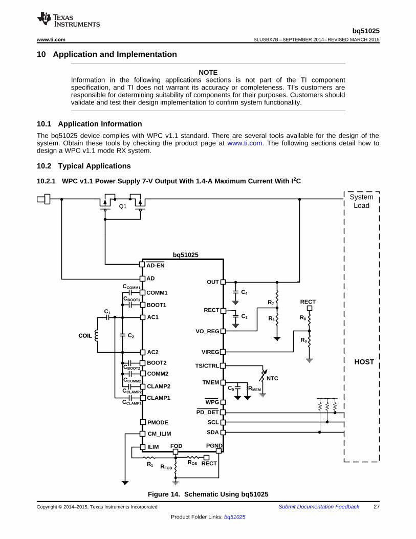
10.2.1 WPC v1.1 Power Supply 7-V Output With 1.4-A Maximum Current With I2C
Figure 14. Schematic Using bq51025
Copyright © 2014–2015, Texas Instruments Incorporated Submit Documentation Feedback 27
Product Folder Links: bq51025

VO 76
VO
K RR
1 K
u
VOOUT
0.5 VK
V
OUT
C4
VO_REG
R7
R6
bq51025SLUSBX7B –SEPTEMBER 2014–REVISED MARCH 2015 www.ti.com
Typical Applications (continued)10.2.1.1 Design Requirements
Table 20. Design ParametersDESIGN PARAMETER EXAMPLE VALUE
VOUT 7 VIOUT MAXIMUM 1.4 A
10.2.1.2 Detailed Design ProcedureTo start the design procedure, determine the following:• Output voltage• Maximum output current
10.2.1.3 Output Voltage Set PointThe output voltage of the bq51025 device can be set by adjusting a feedback resistor divider network. Theresistor divider network is used to set the voltage gain at the VO_REG pin. The device is intended to operatewhere the voltage at the VO_REG pin is set to 0.5 V. This value is the default setting and can be changedthrough I2C. In Figure 15, R6 and R7 are the feedback network for the output voltage sense.
Figure 15. Voltage Gain for Feedback
(12)
(13)
Choose R7 to be a standard value. In this case, take care to choose R6 and R7 to be fairly large values so as tonot dissipate an excessive amount of power in the resistors and thereby lower efficiency.
KVO is set to be 0.5 / 7 = 1/14, choose R7 to be 130 kΩ, and thus R6 to be 10 kΩ.
After R6 and R7 are chosen, the same values should be used on the VI_REG resistor divider (R9 and R8). Thisallows the device to regulate the rectifier voltage properly and accurately track the output voltage.
10.2.1.4 Output and Rectifier CapacitorsSet C4 between 1 and 4.7 µF. This example uses 3.3 µF.
Set C3 between 22 and 44 µF. This example uses 44 µF to minimize output ripple.
28 Submit Documentation Feedback Copyright © 2014–2015, Texas Instruments Incorporated
Product Folder Links: bq51025

1 ILIM FOD5 5 ± 5
ILIMILIM
ILIM
KR
1.2 I
u
1 ILIM FOD5 5 ± 5
ILIMILIM
ILIM
KR
I
ILIM
RFOD
FOD1
R1
RECTROS
bq51025www.ti.com SLUSBX7B –SEPTEMBER 2014–REVISED MARCH 2015
10.2.1.5 TMEMSet C5 to 2.2 µF. To determine the bleedoff resistor, the WPC transmitters (for which the PD_DET is being setfor) needs to be determined. After the ping timing (time between two consecutive digital pings after EPT chargecomplete is sent) is determined, the bleedoff resistor RMEM can be determined. This example uses TI transmitterEVMs as the use case. In this case, the time between pings is 5 s. To set the time constant using Equation 9,RMEM is set to 560 kΩ.
10.2.1.6 Maximum Output Current Set Point
Figure 16. Current Limit Setting for bq51025
The bq51025 device includes a means of providing hardware overcurrent protection by means of an analogcurrent regulation loop. The hardware current limit provides a level of safety by clamping the maximum allowableoutput current (for example, a current compliance). The RILIM resistor size also sets the thresholds for thedynamic rectifier levels, and thus providing efficiency tuning per each application’s maximum system current. Thecalculation for the total RILIM resistance is as follows:
(14)
(15)
The RILIM allows for the ILIM pin to reach 1.2 V at an output current equal to IILIM in 10-W mode and reach 0.6 Vin 5-W mode. When choosing IILIM, consider two possible operating conditions:• If the application requires an output current equal to or greater than external ILIM that the circuit is designed
for (input current limit on the charger where the RX is delivering power to is higher than the external ILIM),ensure that the downstream charger is capable of regulating the voltage of the input into which the RX deviceoutput is tied to by lowering the amount of current being drawn. This ensures that the RX output does notcollapse. Such behavior is referred to as VIN DPM in TI chargers. Unless such behavior is enabled on thecharger, the charger pulls the output of the RX device to ground when the RX device enters currentregulation.
• If the applications are designed to extract less than the IMAX, typical designs should leave a design margin ofat least 20% so that the voltage at ILIM pin reaches 1.2 V when 20% more than maximum current of thesystem (IMAX) is drawn from the output of the RX. Such a design would have input current limit on the chargerlower than the external current limit of the RX device.
In both cases, however, the charger must be capable of regulating the current drawn from the device to allow theoutput voltage to stay at a reasonable value. This same behavior is also necessary during the WPC v1.1Communication. See Communication Current Limit for more details. The following calculations show how such adesign is achieved:
(16)
(17)
Copyright © 2014–2015, Texas Instruments Incorporated Submit Documentation Feedback 29
Product Folder Links: bq51025

( )
( )
12 '
C 2 L1 S S
12 1
C 2 L2 D S C
1
-é ù
= ´ p ´ê úë û
-é ù
= ´ p ´ -ê úê úë û
f
f
495Ö1.7A
842RILIM
bq51025SLUSBX7B –SEPTEMBER 2014–REVISED MARCH 2015 www.ti.com
When referring to the application diagram shown in Figure 16, RILIM is the sum of the R1 and RFOD resistance(that is, the total resistance from the ILIM pin to GND). RFOD is chosen according to the FOD application note thatcan be obtained by contacting your TI representative. This is used to allow the RX implementation to comply withWPC v1.1 requirements related to received power accuracy.
Also note that in many applications, the resistor ROS is necessary to comply with WPC V1.1 requirements. Insuch a case, the offset on the FOD pin from the voltage on RFOD can cause a shift in the calculation that canreduce the expected current limit. Therefore, it is always a good idea to check the output current limit after FODcalibration is performed according to the FOD section. Unfortunately, because the RECT voltage is notdeterministic, and depends on transmitter operation to a certain degree, it is not possible to determine R1 withROS present in a deterministic manner.
In this example, set maximum current for the example to be 1.4 A at 10 W and 700 mA at 5-W mode. Set IILIM =1.7 A to allow for the 20% margin.
(18)
10.2.1.7 I2CThe I2C lines are used to communicate with the device. To enable the I2C, they can be pulled up to an internalhost bus. The device address is 0x6C.
10.2.1.8 Communication Current LimitCommunication current limit allows the device to communicate with the transmitter in an error-free manner bydecoupling the coil from load transients on the OUT pin during WPC communication. In some cases, thiscommunication current limit feature is not desirable. In this design, the user enables the communication currentlimit by tying the CM_ILIM pin to GND. If this is not needed, the CM_ILIM pin can be tied to the OUT pin todisable the communication current limit. In this case, take care that the voltage on the CM_ILIM pin does notexceed the maximum rating of the pin.
10.2.1.9 Receiver CoilThe receiver coil design is the most open part of the system design. The choice of the receiver inductance,shape, and materials all intimately influence the parameters themselves in an intertwined manner. This designcan be complicated and involves optimizing many different aspects; refer to the EVM user's guide (SLUUBSS).
The typical choice of the inductance of the receiver coil for a 10-W, 7-V solution is between 15 and 16 µH.
10.2.1.10 Series and Parallel Resonant CapacitorsResonant capacitors, C1 and C2, are set according to WPC specification.
The equations for calculating the values of the resonant capacitors are shown:
(19)
Because the bq51025 can provide up to 10 W of output power, TI highly recommends that the resonantcapacitors have very-low ESR and dissipate as little power as possible for better thermal performance. TI highlyrecommends NP0/C0G ceramic material capacitors.
10.2.1.11 Communication, Boot, and Clamp CapacitorsSet CCOMMx to a value ranging from C1 / 8 to C1 / 3. The higher the value of the communication capacitors, theeasier it is to comply with the WPC specification. However, higher capacitors do lower the overall efficiency ofthe system. Make sure these are X7R ceramic material and have a minimum voltage rating of 25 V.
Set CBOOTx as 15 nF. Make sure these are X7R ceramic material and have a minimum voltage rating of 25 V.
Set CCLAMPx as 470 nF. Make sure these are X7R ceramic material and have a minimum voltage rating of 25 V.
30 Submit Documentation Feedback Copyright © 2014–2015, Texas Instruments Incorporated
Product Folder Links: bq51025

IOUT (A)
VIL
IM (
V)
0 0.2 0.4 0.6 0.8 1 1.2 1.4 1.6 1.80
0.2
0.4
0.6
0.8
1
1.2
D007
VOUT = 7VROS = Open
RILIM = 495:RILIM = 700:
IOUT (A)
VR
EC
T (
V)
0 0.2 0.4 0.6 0.8 1 1.2 1.46
6.256.5
6.757
7.257.5
7.758
8.258.5
8.759
9.259.5
D008
RILIM = 495:RILIM = 700:
bq51025www.ti.com SLUSBX7B –SEPTEMBER 2014–REVISED MARCH 2015
10.2.1.12 Application Curves
CM_ILIM = High CH1 = VRECT CH2 = VOUT CM_ILIM = High CH1 = VRECT CH2 = VOUTCH3 = PMODE CH4 = ILOAD CH3 = PMODE CH4 = ILOAD
Figure 17. 7-V RX Start-Up With 9-Ω Load on a 5-W WPC Figure 18. 7-V RX Start-Up With 5-Ω Load on a bq500215TX TX
CM_ILIM = High CH1 = VRECT CH2 = VOUT CM_ILIM = High CH1 = VRECT CH2 = VOUTCH4 = ILOAD CH4 = ILOAD
Figure 19. 0- to 1450-mA Step with 7-V RX on bq500215 TX Figure 20. 1450- to 0-mA Load Dump with 7-V RX onbq500215 TX
Figure 22. Rectifier Regulation as a Function of RILIM onFigure 21. ILIM Voltage as a Function of Load Currentbq500215 TX, 7-V RX
Copyright © 2014–2015, Texas Instruments Incorporated Submit Documentation Feedback 31
Product Folder Links: bq51025

VOUT (V)
VR
EC
T (
V)
0 1 2 3 4 5 6 7 8 9 101
2
3
4
5
6
7
8
9
10
D013
IOUT (A)
Fre
quen
cy (
kHz)
0 0.08 0.16 0.24 0.32 0.4 0.48 0.56 0.64 0.72 0.8110
120
130
140
150
160
170
180
190
200
D010
bq500412 (A6)bq500212A (A11)
IOUT (A)
VO
UT (
V)
0 0.2 0.4 0.6 0.8 1 1.2 1.4 1.66.9
6.92
6.94
6.96
6.98
7
7.02
7.04
7.06
7.08
7.1
D009
IOUT (A)
Effi
cien
cy
0 0.08 0.16 0.24 0.32 0.4 0.48 0.56 0.64 0.72 0.80
10%
20%
30%
40%
50%
60%
70%
80%
90%
100%
D011
bq500210 bq500211 bq500412
POUT (W)
Effi
cien
cy
0 1 2 3 4 5 6 7 8 9 100
10%
20%
30%
40%
50%
60%
70%
80%
90%
100%
D0012
VOUT = 5V Wurth 760 308 201 coil VOUT = 7V Vishay IWAS4832FEEB150J50 VOUT= 10V Vishay IWAS4832FEEB150J50
bq51025SLUSBX7B –SEPTEMBER 2014–REVISED MARCH 2015 www.ti.com
CM_ILIM = High CM_ILIM = High
Figure 23. Efficiency on Various 5-W WPC TX, 7-V RX Figure 24. Efficiency on 10-W bq500215 TX
Figure 25. Frequency Range of 7-V, 5-W Mode on a WPC Figure 26. Output Regulation on bq500215 TXTX
CH1 = VRECT CH2 = VOUTCH3 = AD_EN CH4 = AD
Figure 28. AD_EN Functionality upon 5-V USB Connection,Figure 27. VRECT Foldback in Current Limit on a WPC TX10-V RX, No Load
32 Submit Documentation Feedback Copyright © 2014–2015, Texas Instruments Incorporated
Product Folder Links: bq51025

ILOAD(A)
Rep
orte
d R
ecei
ved
Pow
er (
mW
)
Diff
eren
ce b
etw
een
Max
and
Min
Val
ue (
mW
)
0 0.2 0.4 0.6 0.8 1 1.2 1.40 -36
2000 -30
4000 -24
6000 -18
8000 -12
10000 -6
12000 0
D015
MinMaxDifference
bq51025www.ti.com SLUSBX7B –SEPTEMBER 2014–REVISED MARCH 2015
CH1 = VRECT CH2 = VOUTCH3 = AD_EN CH4 = AD
Figure 29. AD_EN Functionality upon 5-V USB Removal, Figure 30. Received Power Variation (mW) vs IOUT (mA) on10-V RX, 1-A Load a WPC TX
CH2 = VTS
Figure 31. TS Voltage Bias Without TS Resistor
Copyright © 2014–2015, Texas Instruments Incorporated Submit Documentation Feedback 33
Product Folder Links: bq51025

COIL
SystemLoad
bq51025
OUT
SCL
AD
AD-EN
WPG
C4
SDA
C1
C2
CBOOT1
AC1
AC2
COIL
BOOT1RECT
C3
NTC
TS/CTRL
CLAMP1CCLAMP1
CCOMM1
COMM1
HOST
PGNDILIM
RFOD
FOD
R1
PD_DET
PMODE
BOOT2CBOOT2
COMM2CCOMM2
CLAMP2CCLAMP2
VO_REG
R6
R7
TMEMC5
CM_ILIM
ROS
R9
R8
VIREG
RECT
R10
Q1
RECT
RMEM
bq51025SLUSBX7B –SEPTEMBER 2014–REVISED MARCH 2015 www.ti.com
10.2.2 Standalone 10-V WPC v1.1 Power Supply With 1-A Maximum Output Current in System BoardWhen the bq5102x device is implemented as an embedded device on the system board, the same designprocedure as for an I2C system should be used, but the I2C pins are to be connected to ground.The VO_REGand VIREG resistor dividers are chosen to achieve 10-V output and RILIM is chosen to allow a maximum currentof 1 A (IILIM = 1.2 A for 20% margin). Refer to WPC v1.1 Power Supply 7-V Output With 1.4-A Maximum CurrentWith I2C for details on how these resistor values are calculated.
A typical coil inductance for 10-V is between 15 and 17 µH. It is important to note that even if the same receivercoil and tuning as for a 7-V RX solution are used (see Receiver Coil and Series and Parallel ResonantCapacitors), the RFOD and ROS values need to be updated to accurately determine the received power.
Figure 32. bq51025 Embedded in a System Board
34 Submit Documentation Feedback Copyright © 2014–2015, Texas Instruments Incorporated
Product Folder Links: bq51025

COIL
SystemLoad
bq51025
OUT
SCL
AD
AD-EN
WPG
C4
SDA
C1
CBOOT1
AC1
AC2
COIL
BOOT1RECT
C3
NTC
TS/CTRL
CLAMP1
CCOMM1
COMM1
HOST
PGNDILIM
RFOD
FOD
R1
PD_DET
PMODE
BOOT2CBOOT2
COMM2CCOMM2
CLAMP2
VO_REG
R6
R7
TMEMC5
CM_ILIM
ROS
R9
R8
VIREG
RECT
RECT
RMEM
DCLAMP
OUT
D1
bq51025www.ti.com SLUSBX7B –SEPTEMBER 2014–REVISED MARCH 2015
10.2.3 Standalone 10-V Power Supply With 1-A Maximum Output Current for 2S Charging SystemFor the bq51025 to work properly as a supply to a 2S charger, the bq51025 output voltage must not drop belowthe minimum input charging voltage of the charger, which may be around 9 V depending on the charger IC. In aWPC tuned Rx/TX system, the power delivered to the load may change during Rx/Tx communication due to thecapacitive modulation when CCOMM1 and CCOMM2 are connected form AC1 and AC2 pins to ground. If the powerdelivered to the load decreases, the VRECT voltage will drop and so may VOUT. if the charger IC does not haveinput DPM. If the power delivered to the load does not change or increases for a given current, the VRECTvoltage will increase and the bq51025 will regulate the voltage.
NOTEThe following design example is for a 2S charging system where the charger IC does nothave input DPM feature.
Figure 33. bq51025 Embedded in a 2S Battery System Board
Copyright © 2014–2015, Texas Instruments Incorporated Submit Documentation Feedback 35
Product Folder Links: bq51025
bq51025SLUSBX7B –SEPTEMBER 2014–REVISED MARCH 2015 www.ti.com
10.2.3.1 Design Requirements
Table 21. Design ParametersDESIGN PARAMETER EXAMPLE VALUE
VOUT 10 VIOUT MAXIMUM 1 A
10.2.3.2 Detailed Design ProcedureTo start the design procedure, determine the following:• Output voltage• Maximum output current
10.2.3.3 Output Voltage Set PointThe output voltage of the bq51025 device can be set by adjusting a feedback resistor divider network asdescribed in Output Voltage Set Point. The ratio of VO_REG and VIREG resistor dividers are chosen to achieve10-V based on the 0.5-V feedback voltage. Following Equation 12 and Equation 13, R6 and R7 are selected tobe 11.3KΩ- and 215-kΩ, respectively. The same values are used on R9 and R8 in the VIREG divider.
10.2.3.4 Output and Rectifier CapacitorsSet C4 to at least 3.3 µF.
Set C3 to at least 44 µF to minimize output ripple. Use capacitors rated for 25 V or higher.
10.2.3.5 TMEMFollow procedure described in TMEM.
10.2.3.6 Maximum Output Current Set PointFollow the procedure described in Maximum Output Current Set Point.
10.2.3.7 I2CConnect I2C lines to ground.
10.2.3.8 Communication Current LimitCommunication current limit must be disabled. Connect CM_ILIM pin to voltage supply making sure it does notexceed maximum absolute rating for the pin. If only the battery voltage is available, use a 5-V Zener diode (D1)to clamp the voltage.
10.2.3.9 Receiver CoilThe receiver coil design is the most open part of the system design. The choice of the receiver inductance,shape, and materials all intimately influence the parameters themselves in an intertwined manner. This designcan be complicated and involves optimizing many different aspects. The typical choice of the inductance of thereceiver coil for a 10-W, 10-V solution is between 15 and 16 µH.
10.2.3.10 Series Resonant CapacitorsIn order for the bq51025 to work properly as a supply to a 2S charger, the bq51025 output voltage must not dropbelow the minimum input charging voltage of the charger, which may be around 9 V depending on the chargerIC. In a WPC tuned Rx/Tx system, the power delivered to the load may change during Rx/Tx communication dueto the capacitive modulation when CCOMM1 and CCOMM2 are connected from AC1 and AC2 pins to ground. If thepower delivered to the load decreases, the VRECT voltage will drop and so may VOUT if the charger IC does nothave VIN-DPM function. If the power delivered to the load does not change or increases for a given current, theVRECT voltage will increase and the bq51025 will regulate the voltage to a fixed value. The following sectiondiscusses the tuning procedure to ensure that the output voltage level is maintained during communication whenoperating with a bq51025 based transmitter.
36 Submit Documentation Feedback Copyright © 2014–2015, Texas Instruments Incorporated
Product Folder Links: bq51025

fLCLk
kLfC
PP
SS SS 4
''
)1(')2(
12
221
'' PS
M
LL
Lk
bq51025www.ti.com SLUSBX7B –SEPTEMBER 2014–REVISED MARCH 2015
10.2.3.10.1 Tuning Procedure
NOTEThe following tuning procedure results in a system that is not compliant with WPCspecification and is only designed to operate with a given bq500215 based transmitter.
1. Measure the effective self-inductance of the bq500215 based transmitter (primary) coil, LP' , and receiver(secondary) coil, LS'. The measurements must be done on the final charging system setup (that is, batteryand any other friendly metal of the device is included as well as any cover material that determines thedistance between the coil and charging surface). Make the measurement at the optimal alignment position.
2. Measure the mutual inductance, LM and calculate the coupling factor given by:
(20)3. A first-order approximation of the series capacitance is given by:
(21)
Where f is the operating frequency of the transmitter, which is 130 kHz and CP is the transmitter resonantcapacitance which is 247 nF.
4. Make sure C1 as well as CCOMM1 and CCOMM2 are populated and place the receiver with best possiblealignment on the transmitter and start power transfer. Using an oscilloscope, monitor the VRECT voltageduring communication at maximum load. If VRECT decreases during communication, increase C1 until thevoltage remains flat. Note that the larger the VRECT voltage increase is during communication at maximumload, the larger the losses on the device. The voltage increase in VRECT is larger with lower load and lowercoupling, so it is important to keep the VRECT voltage as low as possible during communication at maximumload and coupling to maximize efficiency across charging area and load range. Figure 35 and Figure 36show how the VRECT voltage behavior after tuning
10.2.3.11 Communication, Boot, and Clamp CapacitorsSet CCOMMx to a value ranging from C1 / 8 to C1 / 3. Make sure these are X7R ceramic material and have aminimum voltage rating of 25 V. For this example 56-nF capacitors are chosen.
Set CBOOTx as 15 nF. Make sure these are X7R ceramic material and have a minimum voltage rating of 25 V.
CCLAMPx is not populated since a external clamping diode is used.
10.2.3.12 VRECT ClampConnect a 12-V Zener diode (DCLAMP) from VRECT to ground. This diode prevents the rectifier voltage fromovershoot above VRECT-OVP level, preventing unwanted resets during large load transients during communication.
Copyright © 2014–2015, Texas Instruments Incorporated Submit Documentation Feedback 37
Product Folder Links: bq51025

IOUT (A)
Effi
cien
cy
0 0.1 0.2 0.3 0.4 0.5 0.6 0.7 0.8 0.9 10
10%
20%
30%
40%
50%
60%
70%
80%
90%
100%
D016
bq51025SLUSBX7B –SEPTEMBER 2014–REVISED MARCH 2015 www.ti.com
10.2.3.13 Application Curves
CH1 = VRECT CH2 = VOUTCH1 = VRECT CH2 = VOUTCH4 = ILOADCH4 = ILOAD
Figure 35. 10-V Tuned RX VOUT at Center PositionFigure 34. 10-V Tuned RX Start-Up With 1-A LoadWith 1-A Load
CH1 = VRECT CH2 = VOUT CH1 = VRECT CH2 = VOUTCH4 = ILOAD CH4 = ILOAD
Figure 36. 10-V Tuned RX VOUT at Center Position With Figure 37. 1-A to 0-mA Load DumpNo load With 10-V Tuned RX
CH1 = VRECT CH2 = VOUTCH4 = ILOAD
Figure 38. 100-mA to 1-A Load Transient With 10-V Tuned Figure 39. Efficiency With 10-V Tuned RXRX
38 Submit Documentation Feedback Copyright © 2014–2015, Texas Instruments Incorporated
Product Folder Links: bq51025

bq51025www.ti.com SLUSBX7B –SEPTEMBER 2014–REVISED MARCH 2015
11 Power Supply Recommendations
These devices are intended to be operated within the ranges shown in the Recommended Operating Conditions.Because the system involves a loosely coupled inductor setup, the voltages produced on the receiver are afunction of the inductances and the available magnetic field. Ensure that the design in the worst case keeps thevoltages within the Absolute Maximum Ratings.
Copyright © 2014–2015, Texas Instruments Incorporated Submit Documentation Feedback 39
Product Folder Links: bq51025
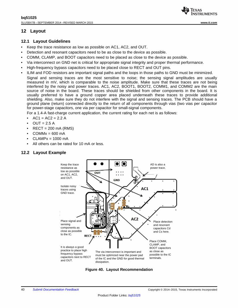
Keep the trace resistance as low as possible on AC1, AC2, and OUT.
Isolate noisy traces using GND trace.
It is always a good practice to place high frequency bypass capacitors next to RECT and OUT.
The via interconnect is important and must be optimized near the power pad of the IC and the GND for good thermal dissipation.
Place COMM, CLAMP, and BOOT capacitors as close as possible to the IC terminals.
Place detection and resonant capacitors Cd and Cs here.
Place signal and sensing components as close as possible to the IC.
AD is also a power trace.
bq51025SLUSBX7B –SEPTEMBER 2014–REVISED MARCH 2015 www.ti.com
12 Layout
12.1 Layout Guidelines• Keep the trace resistance as low as possible on AC1, AC2, and OUT.• Detection and resonant capacitors need to be as close to the device as possible.• COMM, CLAMP, and BOOT capacitors need to be placed as close to the device as possible.• Via interconnect on GND net is critical for appropriate signal integrity and proper thermal performance.• High-frequency bypass capacitors need to be placed close to RECT and OUT pins.• ILIM and FOD resistors are important signal paths and the loops in those paths to GND must be minimized.
Signal and sensing traces are the most sensitive to noise; the sensing signal amplitudes are usuallymeasured in mV, which is comparable to the noise amplitude. Make sure that these traces are not beinginterfered by the noisy and power traces. AC1, AC2, BOOT1, BOOT2, COMM1, and COMM2 are the mainsource of noise in the board. These traces should be shielded from other components in the board. It isusually preferred to have a ground copper area placed underneath these traces to provide additionalshielding. Also, make sure they do not interfere with the signal and sensing traces. The PCB should have aground plane (return) connected directly to the return of all components through vias (two vias per capacitorfor power-stage capacitors, one via per capacitor for small-signal components.For a 1.4-A fast-charge current application, the current rating for each net is as follows:• AC1 = AC2 = 2.2 A• OUT = 2.5 A• RECT = 200 mA (RMS)• COMMx = 600 mA• CLAMPx = 1000 mA• All others can be rated for 10 mA or less.
12.2 Layout Example
Figure 40. Layout Recommendation
40 Submit Documentation Feedback Copyright © 2014–2015, Texas Instruments Incorporated
Product Folder Links: bq51025

bq51025www.ti.com SLUSBX7B –SEPTEMBER 2014–REVISED MARCH 2015
13 Device and Documentation Support
13.1 TrademarksAll trademarks are the property of their respective owners.
13.2 Electrostatic Discharge CautionThese devices have limited built-in ESD protection. The leads should be shorted together or the device placed in conductive foamduring storage or handling to prevent electrostatic damage to the MOS gates.
13.3 GlossarySLYZ022 — TI Glossary.
This glossary lists and explains terms, acronyms, and definitions.
14 Mechanical, Packaging, and Orderable InformationThe following pages include mechanical, packaging, and orderable information. This information is the mostcurrent data available for the designated devices. This data is subject to change without notice and revision ofthis document. For browser-based versions of this data sheet, refer to the left-hand navigation.
Copyright © 2014–2015, Texas Instruments Incorporated Submit Documentation Feedback 41
Product Folder Links: bq51025
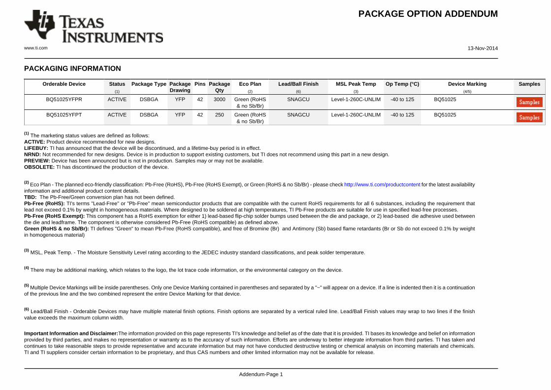
PACKAGE OPTION ADDENDUM
www.ti.com 13-Nov-2014
Addendum-Page 1
PACKAGING INFORMATION
Orderable Device Status(1)
Package Type PackageDrawing
Pins PackageQty
Eco Plan(2)
Lead/Ball Finish(6)
MSL Peak Temp(3)
Op Temp (°C) Device Marking(4/5)
Samples
BQ51025YFPR ACTIVE DSBGA YFP 42 3000 Green (RoHS& no Sb/Br)
SNAGCU Level-1-260C-UNLIM -40 to 125 BQ51025
BQ51025YFPT ACTIVE DSBGA YFP 42 250 Green (RoHS& no Sb/Br)
SNAGCU Level-1-260C-UNLIM -40 to 125 BQ51025
(1) The marketing status values are defined as follows:ACTIVE: Product device recommended for new designs.LIFEBUY: TI has announced that the device will be discontinued, and a lifetime-buy period is in effect.NRND: Not recommended for new designs. Device is in production to support existing customers, but TI does not recommend using this part in a new design.PREVIEW: Device has been announced but is not in production. Samples may or may not be available.OBSOLETE: TI has discontinued the production of the device.
(2) Eco Plan - The planned eco-friendly classification: Pb-Free (RoHS), Pb-Free (RoHS Exempt), or Green (RoHS & no Sb/Br) - please check http://www.ti.com/productcontent for the latest availabilityinformation and additional product content details.TBD: The Pb-Free/Green conversion plan has not been defined.Pb-Free (RoHS): TI's terms "Lead-Free" or "Pb-Free" mean semiconductor products that are compatible with the current RoHS requirements for all 6 substances, including the requirement thatlead not exceed 0.1% by weight in homogeneous materials. Where designed to be soldered at high temperatures, TI Pb-Free products are suitable for use in specified lead-free processes.Pb-Free (RoHS Exempt): This component has a RoHS exemption for either 1) lead-based flip-chip solder bumps used between the die and package, or 2) lead-based die adhesive used betweenthe die and leadframe. The component is otherwise considered Pb-Free (RoHS compatible) as defined above.Green (RoHS & no Sb/Br): TI defines "Green" to mean Pb-Free (RoHS compatible), and free of Bromine (Br) and Antimony (Sb) based flame retardants (Br or Sb do not exceed 0.1% by weightin homogeneous material)
(3) MSL, Peak Temp. - The Moisture Sensitivity Level rating according to the JEDEC industry standard classifications, and peak solder temperature.
(4) There may be additional marking, which relates to the logo, the lot trace code information, or the environmental category on the device.
(5) Multiple Device Markings will be inside parentheses. Only one Device Marking contained in parentheses and separated by a "~" will appear on a device. If a line is indented then it is a continuationof the previous line and the two combined represent the entire Device Marking for that device.
(6) Lead/Ball Finish - Orderable Devices may have multiple material finish options. Finish options are separated by a vertical ruled line. Lead/Ball Finish values may wrap to two lines if the finishvalue exceeds the maximum column width.
Important Information and Disclaimer:The information provided on this page represents TI's knowledge and belief as of the date that it is provided. TI bases its knowledge and belief on informationprovided by third parties, and makes no representation or warranty as to the accuracy of such information. Efforts are underway to better integrate information from third parties. TI has taken andcontinues to take reasonable steps to provide representative and accurate information but may not have conducted destructive testing or chemical analysis on incoming materials and chemicals.TI and TI suppliers consider certain information to be proprietary, and thus CAS numbers and other limited information may not be available for release.

PACKAGE OPTION ADDENDUM
www.ti.com 13-Nov-2014
Addendum-Page 2
In no event shall TI's liability arising out of such information exceed the total purchase price of the TI part(s) at issue in this document sold by TI to Customer on an annual basis.

TAPE AND REEL INFORMATION
*All dimensions are nominal
Device PackageType
PackageDrawing
Pins SPQ ReelDiameter
(mm)
ReelWidth
W1 (mm)
A0(mm)
B0(mm)
K0(mm)
P1(mm)
W(mm)
Pin1Quadrant
BQ51025YFPR DSBGA YFP 42 3000 330.0 12.4 2.99 3.71 0.81 8.0 12.0 Q1
BQ51025YFPT DSBGA YFP 42 250 330.0 12.4 2.99 3.71 0.81 8.0 12.0 Q1
PACKAGE MATERIALS INFORMATION
www.ti.com 13-Nov-2014
Pack Materials-Page 1

*All dimensions are nominal
Device Package Type Package Drawing Pins SPQ Length (mm) Width (mm) Height (mm)
BQ51025YFPR DSBGA YFP 42 3000 367.0 367.0 35.0
BQ51025YFPT DSBGA YFP 42 250 367.0 367.0 35.0
PACKAGE MATERIALS INFORMATION
www.ti.com 13-Nov-2014
Pack Materials-Page 2
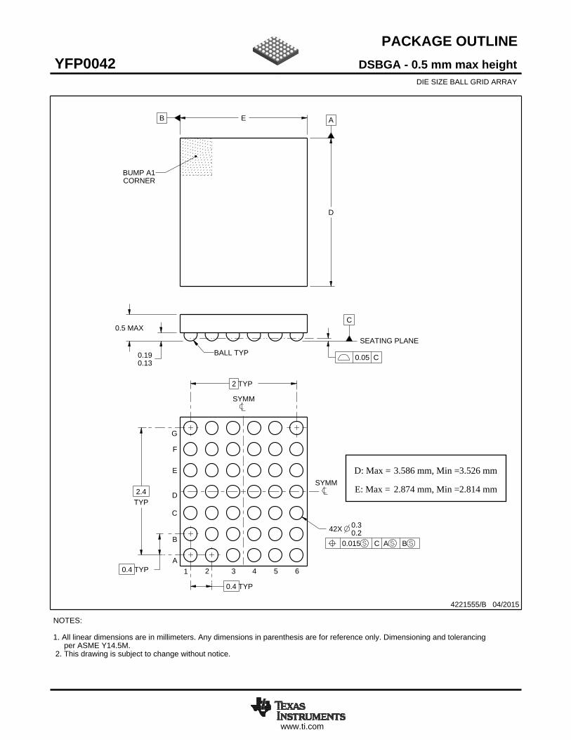
www.ti.com
PACKAGE OUTLINE
C0.5 MAX
0.190.13
2.4TYP
2 TYP
0.4 TYP
0.4 TYP
42X 0.30.2
B E A
D
4221555/B 04/2015
DSBGA - 0.5 mm max heightYFP0042DIE SIZE BALL GRID ARRAY
NOTES: 1. All linear dimensions are in millimeters. Any dimensions in parenthesis are for reference only. Dimensioning and tolerancing per ASME Y14.5M. 2. This drawing is subject to change without notice.
BUMP A1CORNER
SEATING PLANEBALL TYP 0.05 C
A
B
C
D
1 2 3
0.015 C A B
E
54
F
G
6
SYMM
SYMM
SCALE 4.700
D: Max =
E: Max =
3.586 mm, Min =
2.874 mm, Min =
3.526 mm
2.814 mm

www.ti.com
EXAMPLE BOARD LAYOUT
42X ( )0.23(0.4) TYP
(0.4) TYP
( )METAL
0.23 0.05 MAX
SOLDER MASKOPENING
METALUNDERSOLDER MASK
( )SOLDER MASKOPENING
0.23
0.05 MIN
4221555/B 04/2015
DSBGA - 0.5 mm max heightYFP0042DIE SIZE BALL GRID ARRAY
NOTES: (continued) 3. Final dimensions may vary due to manufacturing tolerance considerations and also routing constraints. For more information, see Texas Instruments literature number SNVA009 (www.ti.com/lit/snva009).
SOLDER MASK DETAILSNOT TO SCALE
SYMM
SYMM
LAND PATTERN EXAMPLESCALE:25X
A
B
C
D
1 2 3 4 5
E
F
G
6
NON-SOLDER MASKDEFINED
(PREFERRED)
SOLDER MASKDEFINED

www.ti.com
EXAMPLE STENCIL DESIGN
(0.4)TYP
(0.4) TYP
42X ( 0.25) (R ) TYP0.05
METALTYP
4221555/B 04/2015
DSBGA - 0.5 mm max heightYFP0042DIE SIZE BALL GRID ARRAY
NOTES: (continued) 4. Laser cutting apertures with trapezoidal walls and rounded corners may offer better paste release.
SYMM
SYMM
SOLDER PASTE EXAMPLEBASED ON 0.1 mm THICK STENCIL
SCALE:30X
A
B
C
D
1 2 3
E
4 5 6
F
G

IMPORTANT NOTICE
Texas Instruments Incorporated and its subsidiaries (TI) reserve the right to make corrections, enhancements, improvements and otherchanges to its semiconductor products and services per JESD46, latest issue, and to discontinue any product or service per JESD48, latestissue. Buyers should obtain the latest relevant information before placing orders and should verify that such information is current andcomplete. All semiconductor products (also referred to herein as “components”) are sold subject to TI’s terms and conditions of salesupplied at the time of order acknowledgment.TI warrants performance of its components to the specifications applicable at the time of sale, in accordance with the warranty in TI’s termsand conditions of sale of semiconductor products. Testing and other quality control techniques are used to the extent TI deems necessaryto support this warranty. Except where mandated by applicable law, testing of all parameters of each component is not necessarilyperformed.TI assumes no liability for applications assistance or the design of Buyers’ products. Buyers are responsible for their products andapplications using TI components. To minimize the risks associated with Buyers’ products and applications, Buyers should provideadequate design and operating safeguards.TI does not warrant or represent that any license, either express or implied, is granted under any patent right, copyright, mask work right, orother intellectual property right relating to any combination, machine, or process in which TI components or services are used. Informationpublished by TI regarding third-party products or services does not constitute a license to use such products or services or a warranty orendorsement thereof. Use of such information may require a license from a third party under the patents or other intellectual property of thethird party, or a license from TI under the patents or other intellectual property of TI.Reproduction of significant portions of TI information in TI data books or data sheets is permissible only if reproduction is without alterationand is accompanied by all associated warranties, conditions, limitations, and notices. TI is not responsible or liable for such altereddocumentation. Information of third parties may be subject to additional restrictions.Resale of TI components or services with statements different from or beyond the parameters stated by TI for that component or servicevoids all express and any implied warranties for the associated TI component or service and is an unfair and deceptive business practice.TI is not responsible or liable for any such statements.Buyer acknowledges and agrees that it is solely responsible for compliance with all legal, regulatory and safety-related requirementsconcerning its products, and any use of TI components in its applications, notwithstanding any applications-related information or supportthat may be provided by TI. Buyer represents and agrees that it has all the necessary expertise to create and implement safeguards whichanticipate dangerous consequences of failures, monitor failures and their consequences, lessen the likelihood of failures that might causeharm and take appropriate remedial actions. Buyer will fully indemnify TI and its representatives against any damages arising out of the useof any TI components in safety-critical applications.In some cases, TI components may be promoted specifically to facilitate safety-related applications. With such components, TI’s goal is tohelp enable customers to design and create their own end-product solutions that meet applicable functional safety standards andrequirements. Nonetheless, such components are subject to these terms.No TI components are authorized for use in FDA Class III (or similar life-critical medical equipment) unless authorized officers of the partieshave executed a special agreement specifically governing such use.Only those TI components which TI has specifically designated as military grade or “enhanced plastic” are designed and intended for use inmilitary/aerospace applications or environments. Buyer acknowledges and agrees that any military or aerospace use of TI componentswhich have not been so designated is solely at the Buyer's risk, and that Buyer is solely responsible for compliance with all legal andregulatory requirements in connection with such use.TI has specifically designated certain components as meeting ISO/TS16949 requirements, mainly for automotive use. In any case of use ofnon-designated products, TI will not be responsible for any failure to meet ISO/TS16949.
Products ApplicationsAudio www.ti.com/audio Automotive and Transportation www.ti.com/automotiveAmplifiers amplifier.ti.com Communications and Telecom www.ti.com/communicationsData Converters dataconverter.ti.com Computers and Peripherals www.ti.com/computersDLP® Products www.dlp.com Consumer Electronics www.ti.com/consumer-appsDSP dsp.ti.com Energy and Lighting www.ti.com/energyClocks and Timers www.ti.com/clocks Industrial www.ti.com/industrialInterface interface.ti.com Medical www.ti.com/medicalLogic logic.ti.com Security www.ti.com/securityPower Mgmt power.ti.com Space, Avionics and Defense www.ti.com/space-avionics-defenseMicrocontrollers microcontroller.ti.com Video and Imaging www.ti.com/videoRFID www.ti-rfid.comOMAP Applications Processors www.ti.com/omap TI E2E Community e2e.ti.comWireless Connectivity www.ti.com/wirelessconnectivity
Mailing Address: Texas Instruments, Post Office Box 655303, Dallas, Texas 75265Copyright © 2015, Texas Instruments Incorporated


![HCL Analyst And advisor's day-US V1.1 in attrition ... COPC SAS 70 Compliant OE ... Microsoft PowerPoint - HCL Analyst And advisor's day-US V1.1 [Compatibility Mode] Author: rohankv](https://img.pdfslide.us/doc/110x75/5aeba8067f8b9ad73f8ebcf4/hcl-analyst-and-advisors-day-us-v11-in-attrition-copc-sas-70-compliant-oe.jpg)