Embed Size (px)
Citation preview
Dif
f.In
pu
t
PROG
1.0 MΩ
Coulomb
Counter
SRPSDA
SCL
I2C Bus
1.0 MΩ
SDA
SCL
TEST
CPU
1.8V
LDO
SRN
VDD
1% shunt
Cell
Protection IC
BAT VSS 0.47 µF
FET FET
1 µF
PACKP
PACKN
OTP
Data
Current
ADC
I-Wake
Voltage
ADC
Die TempSensor
10 mΩ,
BAT
Li- Ion
Battery Pack
Copyright © 2017, Texas Instruments Incorporated
Product
Folder
Order
Now
Technical
Documents
Tools &
Software
Support &Community
An IMPORTANT NOTICE at the end of this data sheet addresses availability, warranty, changes, use in safety-critical applications,intellectual property matters and other important disclaimers. PRODUCTION DATA.
bq27411-G1SLUSBN7D –JANUARY 2014–REVISED APRIL 2017
bq27411-G1 Single-Cell Li-Ion Battery Fuel Gauge for Battery Pack Integration
1
1 Features1• Single-Cell Li-Ion Battery Fuel Gauge
– Resides in Battery Pack– Low-Value External Sense Resistor
(10 mΩ Typical)– One Time Programmable (OTP) Configuration
Non-Volatile Memory (NVM)– Powered Directly from Battery with Integrated
LDO– 400-kHz I2C™ Serial Interface– Internal Temperature Sensor or
Host-reported Temperature• Battery Fuel Gauging Based on Patented
Impedance Track™ Technology– Reports Remaining Capacity and State of
Charge (SOC) with Smoothing Filter– Automatically Adjusts for Battery Aging, Self-
discharge, Temperature, and Rate Changes– Battery State of Health (Aging) Estimation
2 Applications• Smartphones, Feature Phones, and Tablets• Digital Still and Video Cameras• Handheld Terminals• MP3 or Multimedia Players
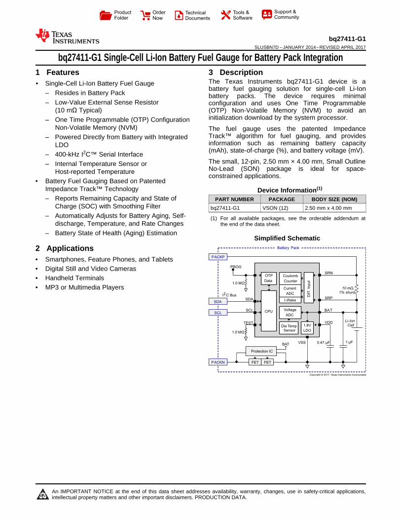
3 DescriptionThe Texas Instruments bq27411-G1 device is abattery fuel gauging solution for single-cell Li-Ionbattery packs. The device requires minimalconfiguration and uses One Time Programmable(OTP) Non-Volatile Memory (NVM) to avoid aninitialization download by the system processor.
The fuel gauge uses the patented ImpedanceTrack™ algorithm for fuel gauging, and providesinformation such as remaining battery capacity(mAh), state-of-charge (%), and battery voltage (mV).
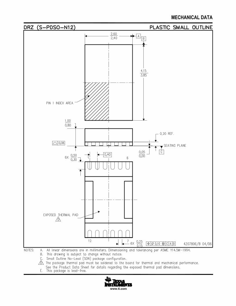
The small, 12-pin, 2.50 mm × 4.00 mm, Small OutlineNo-Lead (SON) package is ideal for space-constrained applications.
Device Information(1)
PART NUMBER PACKAGE BODY SIZE (NOM)bq27411-G1 VSON (12) 2.50 mm x 4.00 mm
(1) For all available packages, see the orderable addendum atthe end of the data sheet.
Simplified Schematic
2
bq27411-G1SLUSBN7D –JANUARY 2014–REVISED APRIL 2017 www.ti.com
Product Folder Links: bq27411-G1
Submit Documentation Feedback Copyright © 2014–2017, Texas Instruments Incorporated
Table of Contents1 Features .................................................................. 12 Applications ........................................................... 13 Description ............................................................. 14 Revision History..................................................... 25 Device Comparison Table ..................................... 36 Pin Configuration and Functions ......................... 37 Specifications......................................................... 4
7.1 Absolute Maximum Ratings ...................................... 47.2 ESD Ratings ............................................................ 47.3 Recommended Operating Conditions....................... 47.4 Thermal Information .................................................. 47.5 Supply Current .......................................................... 57.6 Digital Input and Output DC Characteristics ............. 57.7 LDO Regulator, Wake-Up, and Auto-Shutdown DC
Characteristics ........................................................... 57.8 ADC (Temperature and Cell Measurement)
Characteristics ........................................................... 57.9 Integrating ADC (Coulomb Counter) Characteristics 67.10 I2C-Compatible Interface Communication Timing
Characteristics ........................................................... 67.11 Typical Characteristics ............................................ 7
8 Detailed Description .............................................. 88.1 Overview ................................................................... 88.2 Functional Block Diagram ......................................... 88.3 Feature Description................................................... 88.4 Device Functional Modes.......................................... 98.5 Programming............................................................. 9
9 Applications and Implementation ...................... 139.1 Application Information............................................ 139.2 Typical Applications ................................................ 13
10 Power Supply Recommendation ....................... 1610.1 Power Supply Decoupling..................................... 16
11 Layout................................................................... 1711.1 Layout Guidelines ................................................. 1711.2 Layout Example .................................................... 18
12 Device and Documentation Support ................. 1912.1 Documentation Support ........................................ 1912.2 Trademarks ........................................................... 1912.3 Electrostatic Discharge Caution............................ 1912.4 Glossary ................................................................ 19
13 Mechanical, Packaging, and OrderableInformation ........................................................... 19
4 Revision HistoryNOTE: Page numbers for previous revisions may differ from page numbers in the current version.
Changes from Revision C (September 2015) to Revision D Page
• Changed Simplified Schematic .............................................................................................................................................. 1• Changed Pin Functions PROG description ........................................................................................................................... 3• Changed Figure 5 ................................................................................................................................................................ 13• Changed Figure 6 ................................................................................................................................................................ 14• Changed Power Supply Decoupling .................................................................................................................................... 16• Changed Layout Guidelines ................................................................................................................................................ 17• Changed Figure 10 .............................................................................................................................................................. 18
1SDA 12 PROG
2SCL 11 NC
3VSS
10 TEST
4NC 9 NC
5VDD
8 SRP
6BAT 7 SRN
Not to scale
3
bq27411-G1www.ti.com SLUSBN7D –JANUARY 2014–REVISED APRIL 2017
Product Folder Links: bq27411-G1
Submit Documentation FeedbackCopyright © 2014–2017, Texas Instruments Incorporated
(1) Refer to the CHEM_ID subcommand to confirm the battery chemistry type.(2) Refer to the DM_CODE subcommand to confirm the Data Memory code.(3) Refer to the FW_VERSION subcommand to confirm the firmware version.
5 Device Comparison Table
PART NUMBER BATTERY TYPE CHEM_ID (1) DM_CODE (2) FIRMWAREVERSION (3)
bq27411DRZR-G1A LiCoO2(4.2-V maximum charge) 0x0128 0x80
1.09(0x0109)
bq27411DRZT-G1Abq27411DRZR-G1B LiCoO2
(4.3-V maximum charge) 0x0312 0x90bq27411DRZT-G1Bbq27411DRZR-G1C LiCoO2
(4.35-V maximum charge) 0x0354 0xA0bq27411DRZT-G1C
(1) DIO = Digital input-output, AI = Analog input, P = Power connection
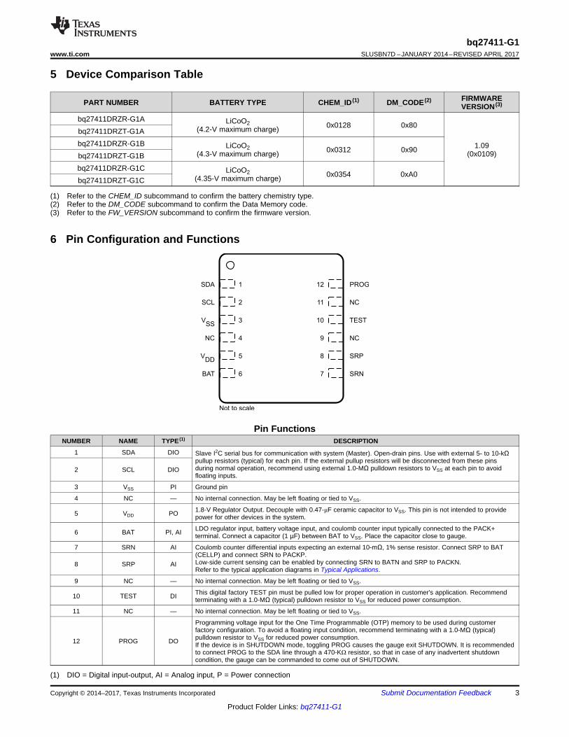
6 Pin Configuration and Functions
Pin FunctionsNUMBER NAME TYPE (1) DESCRIPTION
1 SDA DIO Slave I2C serial bus for communication with system (Master). Open-drain pins. Use with external 5- to 10-kΩpullup resistors (typical) for each pin. If the external pullup resistors will be disconnected from these pinsduring normal operation, recommend using external 1.0-MΩ pulldown resistors to VSS at each pin to avoidfloating inputs.
2 SCL DIO
3 VSS PI Ground pin
4 NC — No internal connection. May be left floating or tied to VSS.
5 VDD PO 1.8-V Regulator Output. Decouple with 0.47-μF ceramic capacitor to VSS. This pin is not intended to providepower for other devices in the system.
6 BAT PI, AI LDO regulator input, battery voltage input, and coulomb counter input typically connected to the PACK+terminal. Connect a capacitor (1 µF) between BAT to VSS. Place the capacitor close to gauge.
7 SRN AI Coulomb counter differential inputs expecting an external 10-mΩ, 1% sense resistor. Connect SRP to BAT(CELLP) and connect SRN to PACKP.Low-side current sensing can be enabled by connecting SRN to BATN and SRP to PACKN.Refer to the typical application diagrams in Typical Applications.
8 SRP AI
9 NC — No internal connection. May be left floating or tied to VSS.
10 TEST DI This digital factory TEST pin must be pulled low for proper operation in customer's application. Recommendterminating with a 1.0-MΩ (typical) pulldown resistor to VSS for reduced power consumption.
11 NC — No internal connection. May be left floating or tied to VSS.
12 PROG DO
Programming voltage input for the One Time Programmable (OTP) memory to be used during customerfactory configuration. To avoid a floating input condition, recommend terminating with a 1.0-MΩ (typical)pulldown resistor to VSS for reduced power consumption.If the device is in SHUTDOWN mode, toggling PROG causes the gauge exit SHUTDOWN. It is recommendedto connect PROG to the SDA line through a 470-KΩ resistor, so that in case of any inadvertent shutdowncondition, the gauge can be commanded to come out of SHUTDOWN.
4
bq27411-G1SLUSBN7D –JANUARY 2014–REVISED APRIL 2017 www.ti.com
Product Folder Links: bq27411-G1
Submit Documentation Feedback Copyright © 2014–2017, Texas Instruments Incorporated
(1) Stresses beyond those listed under "absolute maximum ratings" may cause permanent damage to the device. These are stress ratingsonly, and functional operation of the device at these or any other conditions beyond those indicated under "recommended operatingconditions" is not implied. Exposure to absolute-maximum-rated conditions for extended periods may affect device reliability.
7 Specifications
7.1 Absolute Maximum Ratingsover operating free-air temperature range (unless otherwise noted) (1)
MIN MAX UNITVBAT BAT pin input voltage range –0.3 6 V
VSRSRP and SRN pins input voltage range –0.3 VBAT + 0.3 VDifferential voltage across SRP and SRN. ABS(SRP–SRN) 2 V
VDD VDD pin supply voltage range (LDO output) –0.3 2 VVIOD Open-drain IO pins (SDA, SCL) –0.3 6 VVPROG PROG (pin 12) –0.3 7.8 VVIOPP Push-pull IO pins (TEST, pin 10) –0.3 VDD + 0.3 VTA Operating free-air temperature range –40 85 °CTstg Storage temperature –65 150 °C
(1) JEDEC document JEP155 states that 500-V HBM allows safe manufacturing with a standard ESD control process.(2) JEDEC document JEP157 states that 250-V CDM allows safe manufacturing with a standard ESD control process.
7.2 ESD RatingsVALUE UNIT
V(ESD) Electrostatic dischargeHuman-body model (HBM), per ANSI/ESDA/JEDEC JS-001 (1) ±1500
VCharged-device model (CDM), per JEDEC specification JESD22-C101 (2) ±250
(1) Specified by design. Not production tested.
7.3 Recommended Operating ConditionsTA = 30°C and VREGIN = VBAT = 3.6 V (unless otherwise noted)
MIN NOM MAX UNIT
CBAT(1) External input capacitor for internal
LDO between BAT and VSSNominal capacitor values specified.Recommend a 5% ceramic X5Rtype capacitor located close to thedevice.
0.1 μF
CLDO18(1) External output capacitor for internal
LDO between VDD and VSS0.47 μF
VPU(1) External pull-up voltage for open-
drain pins (SDA, SCL, PROG) 1.62 3.6 V
VPV PROG Programming Voltage [RA0] TA = 15°C to 35°C. OTPProgramming mode only.
7.3 7.4 7.5 VIPV PROG Programming Current [RA0] 4 5 mA
(1) For more information about traditional and new thermal metrics, see the IC Package Thermal Metrics Application Report, SPRA953.
7.4 Thermal Information
THERMAL METRIC (1) bq27411-G1UNIT
DRZ (12 PINS)RθJA Junction-to-ambient thermal resistance 64.1
°C/W
RθJC(top) Junction-to-case (top) thermal resistance 59.8RθJB Junction-to-board thermal resistance 52.7ψJT Junction-to-top characterization parameter 0.3ψJB Junction-to-board characterization parameter 28.3RθJC(bot) Junction-to-case (bottom) thermal resistance 2.4
5
bq27411-G1www.ti.com SLUSBN7D –JANUARY 2014–REVISED APRIL 2017
Product Folder Links: bq27411-G1
Submit Documentation FeedbackCopyright © 2014–2017, Texas Instruments Incorporated
(1) Specified by design. Not production tested.(2) Wake Comparator Disabled
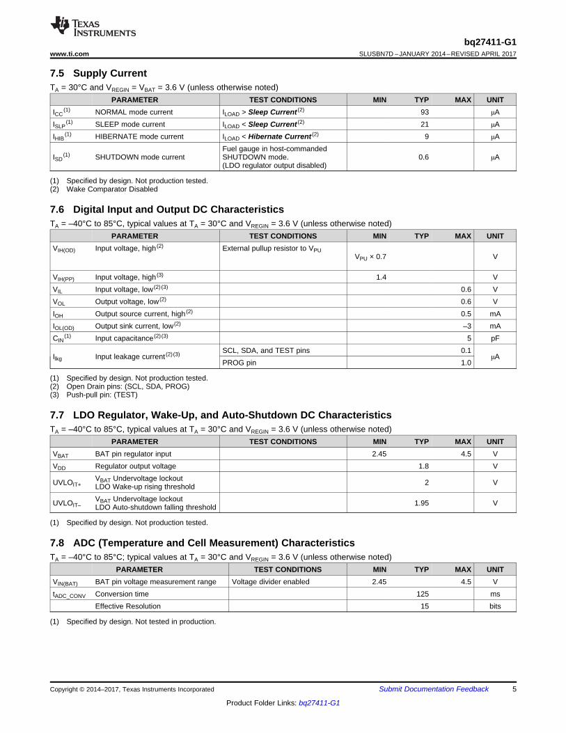
7.5 Supply CurrentTA = 30°C and VREGIN = VBAT = 3.6 V (unless otherwise noted)
PARAMETER TEST CONDITIONS MIN TYP MAX UNITICC
(1) NORMAL mode current ILOAD > Sleep Current (2) 93 μAISLP
(1) SLEEP mode current ILOAD < Sleep Current (2) 21 μAIHIB
(1) HIBERNATE mode current ILOAD < Hibernate Current (2) 9 μA
ISD(1) SHUTDOWN mode current
Fuel gauge in host-commandedSHUTDOWN mode.(LDO regulator output disabled)
0.6 μA
(1) Specified by design. Not production tested.(2) Open Drain pins: (SCL, SDA, PROG)(3) Push-pull pin: (TEST)
7.6 Digital Input and Output DC CharacteristicsTA = –40°C to 85°C, typical values at TA = 30°C and VREGIN = 3.6 V (unless otherwise noted)
PARAMETER TEST CONDITIONS MIN TYP MAX UNITVIH(OD)(ForceNote1) (1)
Input voltage, high (2) External pullup resistor to VPUVPU × 0.7 V
VIH(PP) Input voltage, high (3) 1.4 VVIL Input voltage, low (2) (3) 0.6 VVOL Output voltage, low (2) 0.6 VIOH Output source current, high (2) 0.5 mAIOL(OD) Output sink current, low (2) –3 mACIN
(1) Input capacitance (2) (3) 5 pF
Ilkg Input leakage current (2) (3) SCL, SDA, and TEST pins 0.1μA
PROG pin 1.0
(1) Specified by design. Not production tested.
7.7 LDO Regulator, Wake-Up, and Auto-Shutdown DC CharacteristicsTA = –40°C to 85°C, typical values at TA = 30°C and VREGIN = 3.6 V (unless otherwise noted)(Force Note1) (1)
PARAMETER TEST CONDITIONS MIN TYP MAX UNITVBAT BAT pin regulator input 2.45 4.5 VVDD Regulator output voltage 1.8 V
UVLOIT+VBAT Undervoltage lockoutLDO Wake-up rising threshold 2 V
UVLOIT–VBAT Undervoltage lockoutLDO Auto-shutdown falling threshold 1.95 V
(1) Specified by design. Not tested in production.
7.8 ADC (Temperature and Cell Measurement) CharacteristicsTA = –40°C to 85°C; typical values at TA = 30°C and VREGIN = 3.6 V (unless otherwise noted) (Force Note1) (1)
PARAMETER TEST CONDITIONS MIN TYP MAX UNITVIN(BAT) BAT pin voltage measurement range Voltage divider enabled 2.45 4.5 VtADC_CONV Conversion time 125 ms
Effective Resolution 15 bits
6
bq27411-G1SLUSBN7D –JANUARY 2014–REVISED APRIL 2017 www.ti.com
Product Folder Links: bq27411-G1
Submit Documentation Feedback Copyright © 2014–2017, Texas Instruments Incorporated
(1) Specified by design. Not tested in production.
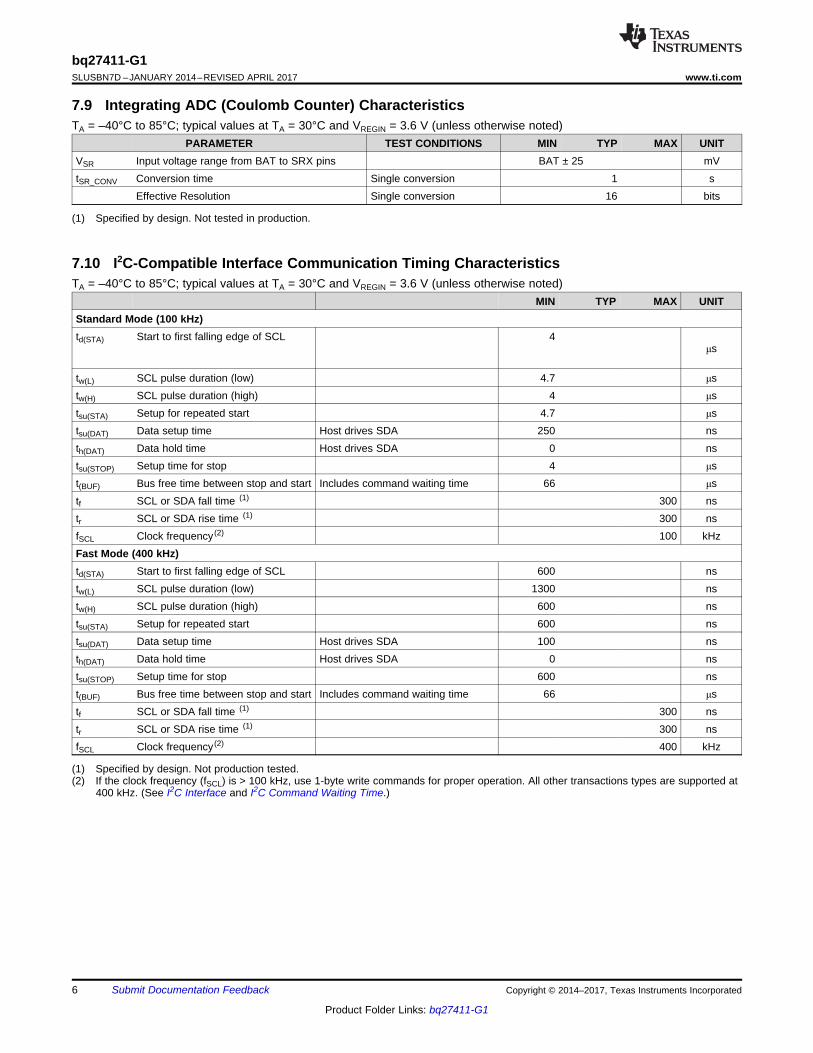
7.9 Integrating ADC (Coulomb Counter) CharacteristicsTA = –40°C to 85°C; typical values at TA = 30°C and VREGIN = 3.6 V (unless otherwise noted)(Force Note1) (1)
PARAMETER TEST CONDITIONS MIN TYP MAX UNITVSR Input voltage range from BAT to SRX pins BAT ± 25 mVtSR_CONV Conversion time Single conversion 1 s
Effective Resolution Single conversion 16 bits
(1) Specified by design. Not production tested.(2) If the clock frequency (fSCL) is > 100 kHz, use 1-byte write commands for proper operation. All other transactions types are supported at
400 kHz. (See I2C Interface and I2C Command Waiting Time.)
7.10 I2C-Compatible Interface Communication Timing CharacteristicsTA = –40°C to 85°C; typical values at TA = 30°C and VREGIN = 3.6 V (unless otherwise noted)
MIN TYP MAX UNITStandard Mode (100 kHz)td(STA)(ForceNote1) (1)
Start to first falling edge of SCL 4μs
tw(L) SCL pulse duration (low) 4.7 μstw(H) SCL pulse duration (high) 4 μstsu(STA) Setup for repeated start 4.7 μstsu(DAT) Data setup time Host drives SDA 250 nsth(DAT) Data hold time Host drives SDA 0 nstsu(STOP) Setup time for stop 4 μst(BUF) Bus free time between stop and start Includes command waiting time 66 μstf SCL or SDA fall time (1) 300 nstr SCL or SDA rise time (1) 300 nsfSCL Clock frequency (2) 100 kHzFast Mode (400 kHz)td(STA) Start to first falling edge of SCL 600 nstw(L) SCL pulse duration (low) 1300 nstw(H) SCL pulse duration (high) 600 nstsu(STA) Setup for repeated start 600 nstsu(DAT) Data setup time Host drives SDA 100 nsth(DAT) Data hold time Host drives SDA 0 nstsu(STOP) Setup time for stop 600 nst(BUF) Bus free time between stop and start Includes command waiting time 66 μstf SCL or SDA fall time (1) 300 nstr SCL or SDA rise time (1) 300 nsfSCL Clock frequency (2) 400 kHz
Temperature (°C)
Cur
rent
Acc
urac
y E
rror
(%
)
-40 -20 0 20 40 60 80 100-0.6
-0.5
-0.4
-0.3
-0.2
-0.1
0
Temperature (°C)
Vol
tage
Acc
urac
y E
rror
(%
)
-40 -20 0 20 40 60 80 1000.02
0.04
0.06
0.08
0.1
0.12
0.14
Temperature (°C)
Tem
pera
ture
Acc
urac
y E
rror
(%)
-40 -20 0 20 40 60 80 100-15
-10
-5
0
5
10
tSU(STA)
SCL
SDA
tw(H) tw(L)tf tr t(BUF)
tr
td(STA)
REPEATEDSTART
th(DAT) tsu(DAT)
tf tsu(STOP)
STOP START
7
bq27411-G1www.ti.com SLUSBN7D –JANUARY 2014–REVISED APRIL 2017
Product Folder Links: bq27411-G1
Submit Documentation FeedbackCopyright © 2014–2017, Texas Instruments Incorporated
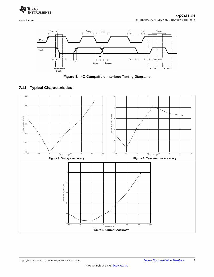
Figure 1. I2C-Compatible Interface Timing Diagrams
7.11 Typical Characteristics
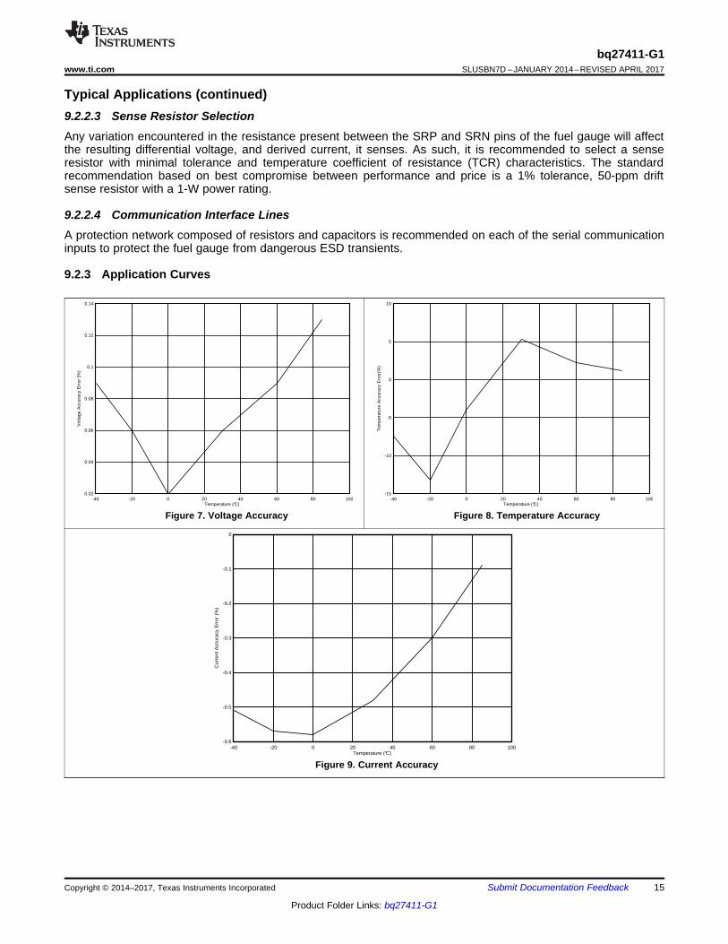
Figure 2. Voltage Accuracy Figure 3. Temperature Accuracy
Figure 4. Current Accuracy
Dif
f.In
pu
t
PROG
1.0 MΩ
Coulomb
Counter
SRPSDA
SCL
I2C Bus
1.0 MΩ
SDA
SCL
TEST
CPU
1.8V
LDO
SRN
VDD
1% shunt
Cell
Protection IC
BAT VSS 0.47 µF
FET FET
1 µF
PACKP
PACKN
OTP
Data
Current
ADC
I-Wake
Voltage
ADC
Die TempSensor
10 mΩ,
BAT
Li- Ion
Battery Pack
Copyright © 2017, Texas Instruments Incorporated
8
bq27411-G1SLUSBN7D –JANUARY 2014–REVISED APRIL 2017 www.ti.com
Product Folder Links: bq27411-G1
Submit Documentation Feedback Copyright © 2014–2017, Texas Instruments Incorporated
8 Detailed Description
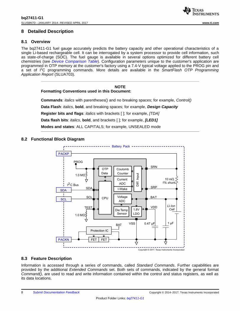
8.1 OverviewThe bq27411-G1 fuel gauge accurately predicts the battery capacity and other operational characteristics of asingle Li-based rechargeable cell. It can be interrogated by a system processor to provide cell information, suchas state-of-charge (SOC). The fuel gauge is available in several options optimized for different battery cellchemistries (see Device Comparison Table). Configuration parameters unique to the customer's application areprogrammed in OTP memory at the customer's factory using a 7.4-V typical voltage applied to the PROG pin anda set of I2C programming commands. More details are available in the SmartFlash OTP ProgrammingApplication Report (SLUA703).
NOTEFormatting Conventions used in this Document:
Commands: italics with parentheses() and no breaking spaces; for example, Control()
Data Flash: italics, bold, and breaking spaces; for example, Design CapacityRegister bits and flags: italics with brackets [ ]; for example, [TDA]
Data flash bits: italics, bold, and brackets [ ]; for example, [LED1]Modes and states: ALL CAPITALS; for example, UNSEALED mode
8.2 Functional Block Diagram
8.3 Feature DescriptionInformation is accessed through a series of commands, called Standard Commands. Further capabilities areprovided by the additional Extended Commands set. Both sets of commands, indicated by the general formatCommand(), are used to read and write information contained within the control and status registers, as well asits data locations.
9
bq27411-G1www.ti.com SLUSBN7D –JANUARY 2014–REVISED APRIL 2017
Product Folder Links: bq27411-G1
Submit Documentation FeedbackCopyright © 2014–2017, Texas Instruments Incorporated
Feature Description (continued)The key to the high-accuracy gas gauging prediction is Texas Instruments proprietary Impedance Trackalgorithm. This algorithm uses cell measurements, characteristics, and properties to create state-of-chargepredictions that can achieve high accuracy across a wide variety of operating conditions and over the lifetime ofthe battery.
The fuel gauge measures the charging or discharging of the battery by monitoring the voltage across a small-value sense resistor. When a cell is attached to the fuel gauge, cell impedance is computed, based on cellcurrent, cell open-circuit voltage (OCV), and cell voltage under loading conditions.
The fuel gauge uses an integrated temperature sensor for estimating cell temperature. Alternatively, the hostprocessor can provide temperature data for the fuel gauge.
For more details, see the bq27411-G1 Technical Reference Manual (SLUUAS7).
8.4 Device Functional ModesTo minimize power consumption, the fuel gauge has several power modes: INITIALIZATION, NORMAL, SLEEP,and HIBERNATE. The fuel gauge passes automatically between these modes, depending upon the occurrenceof specific events, though a system processor can initiate some of these modes directly.
For more details, see the bq27411-G1 Technical Reference Manual (SLUUAS7).
8.5 Programming
8.5.1 Standard Data CommandsThe bq27411-G1 fuel gauge uses a series of 2-byte standard commands to enable system reading and writing ofbattery information. Each standard command has an associated command-code pair, as indicated in Table 1.Because each command consists of two bytes of data, two consecutive I2C transmissions must be executed bothto initiate the command function, and to read or write the corresponding two bytes of data. For more details, seethe bq27411-G1 Technical Reference Manual (SLUUAS7).
Table 1. Standard CommandsNAME COMMAND
CODEUNIT SEALED
ACCESSControl() CNTL 0x00 and 0x01 NA R/WTemperature() TEMP 0x02 and 0x03 0.1°K R/WVoltage() VOLT 0x04 and 0x05 mV RFlags() FLAGS 0x06 and 0x07 NA RNominalAvailableCapacity() 0x08 and 0x09 mAh RFullAvailableCapacity() 0x0A and 0x0B mAh RRemainingCapacity() RM 0x0C and 0x0D mAh RFullChargeCapacity() FCC 0x0E and 0x0F mAh RAverageCurrent() 0x10 and 0x11 mA RStandbyCurrent() 0x12 and 0x13 mA RMaxLoadCurrent() 0x14 and 0x15 mA RAveragePower() 0x18 and 0x19 mW RStateOfCharge() SOC 0x1C and 0x1D % RInternalTemperature() 0x1E and 0x1F 0.1°K RStateOfHealth() SOH 0x20 and 0x21 num / % RRemainingCapacityUnfiltered() 0x28 and 0x29 mAh RRemainingCapacityFiltered() 0x2A and 0x2B mAh RFullChargeCapacityUnfiltered() 0x2C and 0x2D mAh RFullChargeCapacityFiltered() 0x2E and 0x2F mAh RStateOfChargeUnfiltered() 0x30 and 0x31 % R
10
bq27411-G1SLUSBN7D –JANUARY 2014–REVISED APRIL 2017 www.ti.com
Product Folder Links: bq27411-G1
Submit Documentation Feedback Copyright © 2014–2017, Texas Instruments Incorporated
8.5.2 Control(): 0x00 and 0x01Issuing a Control() command requires a subsequent 2-byte subcommand. These additional bytes specify theparticular control function desired. The Control() command allows the system to control specific features of thefuel gauge during normal operation and additional features when the device is in different access modes, asdescribed in Table 2. For additional details, see the bq27411-G1 Technical Reference Manual (SLUUAS7).
Table 2. Control() Subcommands
CONTROL FUNCTION CONTROLDATA SEALED ACCESS DESCRIPTION
CONTROL_STATUS 0x0000 Yes Reports the status of deviceDEVICE_TYPE 0x0001 Yes Reports the device type (0x0421)FW_VERSION 0x0002 Yes Reports the firmware version of the deviceDM_CODE 0x0004 Yes Reports the Data Memory Code number stored in OTP memoryPREV_MACWRITE 0x0007 Yes Returns previous MAC command codeCHEM_ID 0x0008 Yes Reports the chemical identifier of the battery profile currently
used by the Impedance Track configurationSET_HIBERNATE 0x0011 Yes Forces CONTROL_STATUS [HIBERNATE] to 1CLEAR_HIBERNATE 0x0012 Yes Forces CONTROL_STATUS [HIBERNATE] to 0SET_CFGUPDATE 0x0013 No Forces CONTROL_STATUS [CFGUPMODE] to 1 and gauge
enters CONFIG UPDATE modeSEALED 0x0020 No Places the device in SEALED access modeRESET 0x0041 No Performs a full device resetSOFT_RESET 0x0042 No Gauge exits CONFIG UPDATE mode
(1) SEALED and UNSEALED states are entered via commands to Control() 0x00 and 0x01(2) In SEALED mode, data cannot be accessed through commands 0x3E and 0x3F.
8.5.3 Extended Data CommandsExtended data commands offer additional functionality beyond the standard set of commands. They are used inthe same manner; however, unlike standard commands, extended commands are not limited to 2-byte words.The number of command bytes for a given extended command ranges in size from single to multiple bytes, asspecified in Table 3.
Table 3. Extended Commands
Name Command Code Unit SEALEDAccess (1) (2)
UNSEALEDAccess (1) (2)
OpConfig() 0x3A and 0x3B NA R RDesignCapacity() 0x3C and 0x3D mAh R RDataClass() (2) 0x3E NA NA RWDataBlock() (2) 0x3F NA RW RWBlockData() 0x40 through 0x5F NA R RWBlockDataCheckSum() 0x60 NA RW RWBlockDataControl() 0x61 NA NA RWReserved 0x62 through 0x7F NA R R
8.5.4 Communications
8.5.4.1 I2C InterfaceThe bq27411-G1 fuel gauge supports the standard I2C read, incremental read, quick read, one-byte write, andincremental write functions. The 7-bit device address (ADDR) is the most significant 7 bits of the hex addressand is fixed as 1010101. The first 8 bits of the I2C protocol are, therefore, 0xAA or 0xAB for write or read,respectively.

Host generated
A AS 0ADDR[6:0] CMD[7:0] Sr 1ADDR[6:0] A DATA [7:0] A DATA [7:0] PN. . .
(d) incremental read
A AS 0ADDR[6:0] CMD[7:0] Sr 1ADDR[6:0] A DATA [7:0] PN
(c) 1- byte read
A AS A0 PADDR[6:0] CMD[7:0] DATA [7:0]
(a) 1-byte write (b) quick read
S 1ADDR[6:0] A DATA [7:0] PN
Gauge generated
. . .A AS A0 PADDR[6:0] CMD[7:0] DATA [7:0] DATA [7:0] A A
(e) incremental write
(S = Start , Sr = Repeated Start , A = Acknowledge , N = No Acknowledge , and P = Stop).
11
bq27411-G1www.ti.com SLUSBN7D –JANUARY 2014–REVISED APRIL 2017
Product Folder Links: bq27411-G1
Submit Documentation FeedbackCopyright © 2014–2017, Texas Instruments Incorporated
The quick read returns data at the address indicated by the address pointer. The address pointer, a registerinternal to the I2C communication engine, increments whenever data is acknowledged by the fuel gauge or theI2C master. “Quick writes” function in the same manner and are a convenient means of sending multiple bytes toconsecutive command locations (such as two-byte commands that require two bytes of data).
The following command sequences are not supported:Attempt to write a read-only address (NACK after data sent by master):
Attempt to read an address above 0x6B (NACK command):
8.5.4.2 I2C Time OutThe I2C engine releases both SDA and SCL if the I2C bus is held low for 2 seconds. If the fuel gauge is holdingthe lines, releasing them frees them for the master to drive the lines. If an external condition is holding either ofthe lines low, the I2C engine enters the low-power SLEEP mode.
8.5.4.3 I2C Command Waiting TimeTo ensure proper operation at 400 kHz, a t(BUF) ≥ 66-μs bus-free waiting time must be inserted between allpackets addressed to the fuel gauge. In addition, if the SCL clock frequency (fSCL) is > 100 kHz, use individual 1-byte write commands for proper data flow control. The following diagram shows the standard waiting timerequired between issuing the control subcommand the reading the status result. For read-write standardcommand, a minimum of 2 seconds is required to get the result updated. For read-only standard commands,there is no waiting time required, but the host must not issue any standard command more than two times persecond. Otherwise, the gauge could result in a reset issue due to the expiration of the watchdog timer.
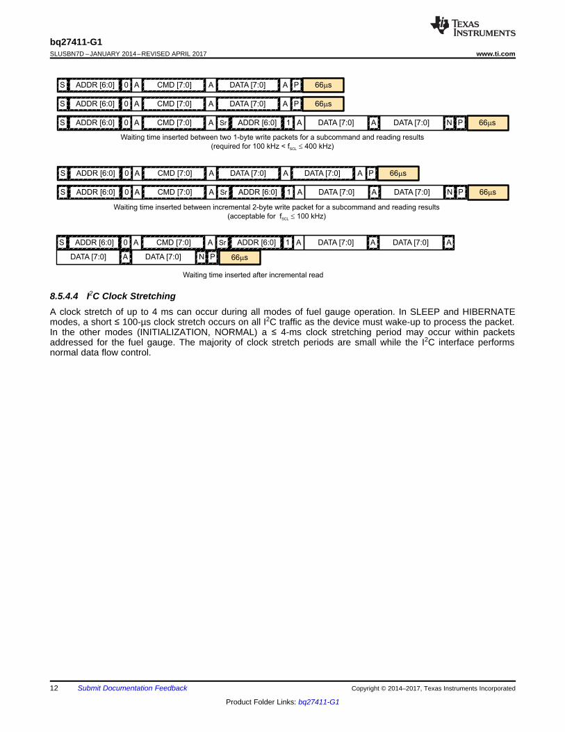
A AS 0ADDR [6:0] CMD [7:0] Sr 1ADDR [6:0] A DATA [7:0] A DATA [7:0] PN
A AS A0 PADDR [6:0] CMD [7:0] DATA [7:0] DATA [7:0] A 66 sm
A AS 0ADDR [6:0] CMD [7:0] Sr 1ADDR [6:0] A DATA [7:0] A DATA [7:0] A
DATA [7:0] A DATA [7:0] PN
Waiting time inserted between incremental 2-byte write packet for a subcommand and reading results
(acceptable for 100 kHz)fSCL £
Waiting time inserted after incremental read
66 sm
66 sm
A AS 0ADDR [6:0] CMD [7:0] Sr 1ADDR [6:0] A DATA [7:0] A DATA [7:0] PN
A AS A0 PADDR [6:0] CMD [7:0] DATA [7:0] 66 sm
Waiting time inserted between two 1-byte write packets for a subcommand and reading results
(required for 100 kHz < f 400 kHz)SCL £
66 sm
A AS A0 PADDR [6:0] CMD [7:0] DATA [7:0] 66 sm
12
bq27411-G1SLUSBN7D –JANUARY 2014–REVISED APRIL 2017 www.ti.com
Product Folder Links: bq27411-G1
Submit Documentation Feedback Copyright © 2014–2017, Texas Instruments Incorporated
8.5.4.4 I2C Clock StretchingA clock stretch of up to 4 ms can occur during all modes of fuel gauge operation. In SLEEP and HIBERNATEmodes, a short ≤ 100-µs clock stretch occurs on all I2C traffic as the device must wake-up to process the packet.In the other modes (INITIALIZATION, NORMAL) a ≤ 4-ms clock stretching period may occur within packetsaddressed for the fuel gauge. The majority of clock stretch periods are small while the I2C interface performsnormal data flow control.
13
PW
PD
C2
R10100 100
C4
150 pF
R6 R71 M 300
R8 R9300 1 M
C5
150 pF
PGND PGND
PROG
TP1
PGND
C1
0.47 µF
1SDA
2SCL
3VSS
4NC
5VDD
6BAT
U1
PROG 12
NC11
TEST 10
NC 9
SRP8
SRN 7
R5
1.0 M
R41.0 M
PGND PGND
J1
CELLP 1 1
J2
1
2 Note: SDA and SCL
Require 5 Kohm
CELLN 22 1.0 µF 3 pullups provided by
system
PGND
R1
0. 010
4
Optional ESD Filter
SCL
SDA
SCL
SDAt :No e 1% Tolerance
PGND
PGND
R11
SCL
PACKP
SDA
PACKN
13
bq27411-G1www.ti.com SLUSBN7D –JANUARY 2014–REVISED APRIL 2017
Product Folder Links: bq27411-G1
Submit Documentation FeedbackCopyright © 2014–2017, Texas Instruments Incorporated
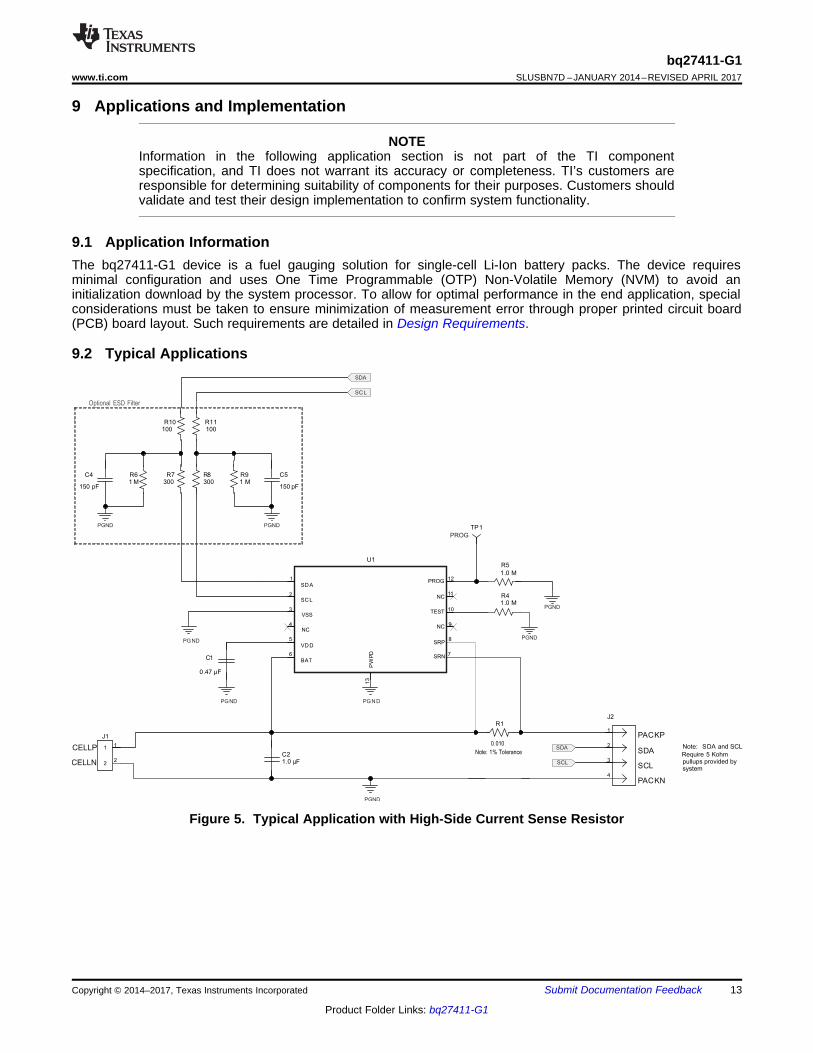
9 Applications and Implementation
NOTEInformation in the following application section is not part of the TI componentspecification, and TI does not warrant its accuracy or completeness. TI’s customers areresponsible for determining suitability of components for their purposes. Customers shouldvalidate and test their design implementation to confirm system functionality.
9.1 Application InformationThe bq27411-G1 device is a fuel gauging solution for single-cell Li-Ion battery packs. The device requiresminimal configuration and uses One Time Programmable (OTP) Non-Volatile Memory (NVM) to avoid aninitialization download by the system processor. To allow for optimal performance in the end application, specialconsiderations must be taken to ensure minimization of measurement error through proper printed circuit board(PCB) board layout. Such requirements are detailed in Design Requirements.
9.2 Typical Applications
Figure 5. Typical Application with High-Side Current Sense Resistor
13
PW
PD
C2
R10100 100
C4
150 pF
R6 R71 M 300
R8 R9300 1 M
C5
150 pF
PGND PGND
PROG
TP1
PGND
C1
0.47 µF
1SDA
2SCL
3VSS
4NC
5VDD
6BAT
U1
PROG12
NC11
TEST10
NC9
SRP8
SRN7
R5
1.0 M
R41.0 M
PGND PGND
J1
CELLP 1 1
J2
1
2 Note: SDA and SCL
Require 5-KΩ
CELLN 22 1.0 µF 3 pullups provided by
the system
PGND
R1
0. 010
4
Optional ESD Filter
SCL
SDA
SCL
SDA
t :No e 1% Tolerance
PGND
PGND
R11
SCL
PACKP
SDA
PACKN
14
bq27411-G1SLUSBN7D –JANUARY 2014–REVISED APRIL 2017 www.ti.com
Product Folder Links: bq27411-G1
Submit Documentation Feedback Copyright © 2014–2017, Texas Instruments Incorporated
Typical Applications (continued)
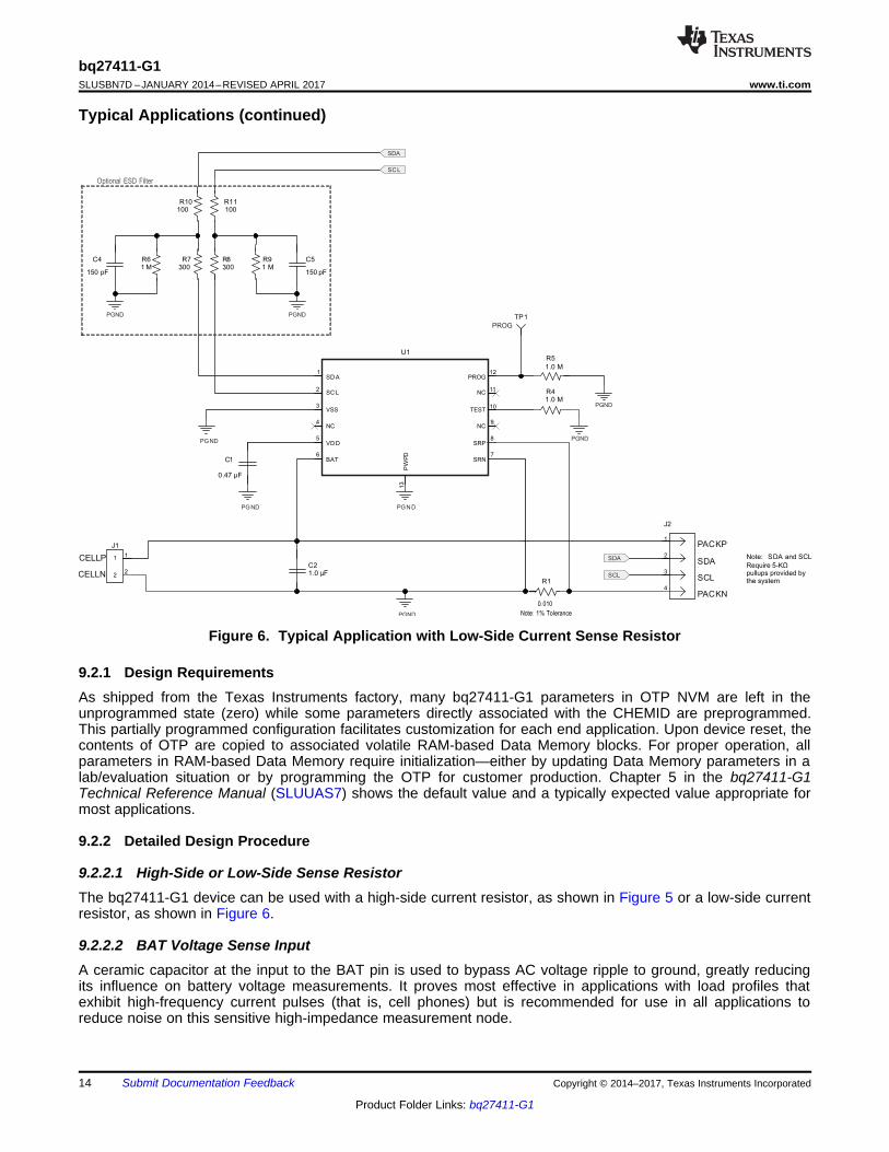
Figure 6. Typical Application with Low-Side Current Sense Resistor
9.2.1 Design RequirementsAs shipped from the Texas Instruments factory, many bq27411-G1 parameters in OTP NVM are left in theunprogrammed state (zero) while some parameters directly associated with the CHEMID are preprogrammed.This partially programmed configuration facilitates customization for each end application. Upon device reset, thecontents of OTP are copied to associated volatile RAM-based Data Memory blocks. For proper operation, allparameters in RAM-based Data Memory require initialization—either by updating Data Memory parameters in alab/evaluation situation or by programming the OTP for customer production. Chapter 5 in the bq27411-G1Technical Reference Manual (SLUUAS7) shows the default value and a typically expected value appropriate formost applications.
9.2.2 Detailed Design Procedure
9.2.2.1 High-Side or Low-Side Sense ResistorThe bq27411-G1 device can be used with a high-side current resistor, as shown in Figure 5 or a low-side currentresistor, as shown in Figure 6.
9.2.2.2 BAT Voltage Sense InputA ceramic capacitor at the input to the BAT pin is used to bypass AC voltage ripple to ground, greatly reducingits influence on battery voltage measurements. It proves most effective in applications with load profiles thatexhibit high-frequency current pulses (that is, cell phones) but is recommended for use in all applications toreduce noise on this sensitive high-impedance measurement node.
Temperature (°C)
Cur
rent
Acc
urac
y E
rror
(%
)
-40 -20 0 20 40 60 80 100-0.6
-0.5
-0.4
-0.3
-0.2
-0.1
0
Temperature (°C)
Vol
tage
Acc
urac
y E
rror
(%
)
-40 -20 0 20 40 60 80 1000.02
0.04
0.06
0.08
0.1
0.12
0.14
Temperature (°C)
Tem
pera
ture
Acc
urac
y E
rror
(%)
-40 -20 0 20 40 60 80 100-15
-10
-5
0
5
10
15
bq27411-G1www.ti.com SLUSBN7D –JANUARY 2014–REVISED APRIL 2017
Product Folder Links: bq27411-G1
Submit Documentation FeedbackCopyright © 2014–2017, Texas Instruments Incorporated
Typical Applications (continued)9.2.2.3 Sense Resistor SelectionAny variation encountered in the resistance present between the SRP and SRN pins of the fuel gauge will affectthe resulting differential voltage, and derived current, it senses. As such, it is recommended to select a senseresistor with minimal tolerance and temperature coefficient of resistance (TCR) characteristics. The standardrecommendation based on best compromise between performance and price is a 1% tolerance, 50-ppm driftsense resistor with a 1-W power rating.
9.2.2.4 Communication Interface LinesA protection network composed of resistors and capacitors is recommended on each of the serial communicationinputs to protect the fuel gauge from dangerous ESD transients.
9.2.3 Application Curves
Figure 7. Voltage Accuracy Figure 8. Temperature Accuracy
Figure 9. Current Accuracy
16
bq27411-G1SLUSBN7D –JANUARY 2014–REVISED APRIL 2017 www.ti.com
Product Folder Links: bq27411-G1
Submit Documentation Feedback Copyright © 2014–2017, Texas Instruments Incorporated
10 Power Supply Recommendation
10.1 Power Supply DecouplingThe battery connection on the BAT pin is used for two purposes:• To supply power to the fuel gauge• As an input for voltage measurement of the battery
A capacitor of value of at least 1 µF should be connected between BAT and VSS. The capacitor should be placedclose to the gauge IC and have short traces to both the VDD pin and VSS.
The fuel gauge has an integrated LDO with an output on the VDD pin of approximately 1.8 V. A capacitor of valueat least 0.47 μF should be connected between the VDD pin and VSS. The capacitor should be placed close to thegauge IC and have short traces to both the VDD pin and VSS.
17
bq27411-G1www.ti.com SLUSBN7D –JANUARY 2014–REVISED APRIL 2017
Product Folder Links: bq27411-G1
Submit Documentation FeedbackCopyright © 2014–2017, Texas Instruments Incorporated
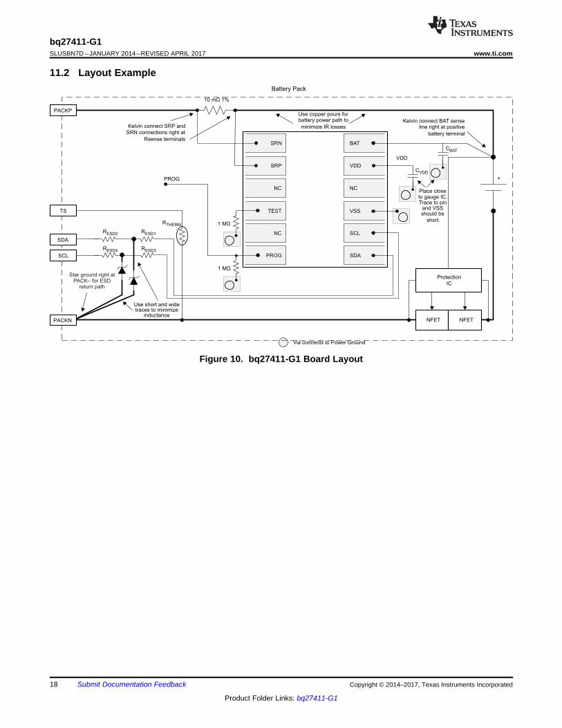
11 Layout
11.1 Layout Guidelines• A capacitor, of value at least 0.47 µF, is connected between the VDD pin and VSS. The capacitor should be
placed close to the gauge IC and have short traces to both the VDD pin and VSS.• It is required to have a capacitor, at least 1.0 µF, connect between the BAT pin and VSS if the connection
between the battery pack and the gauge BAT pin has the potential to pick up noise. The capacitor should beplaced close to the gauge IC and have short traces to both the VDD pin and VSS.
• If the external pullup resistors on the SCL and SDA lines will be disconnected from the host during low-poweroperation, it is recommended to use external 1-MΩ pulldown resistors to VSS to avoid floating inputs to the I2Cengine.
• The value of the SCL and SDA pullup resistors should take into consideration the pullup voltage and the buscapacitance. Some recommended values, assuming a bus capacitance of 10 pF, can be seen in Table 4.
Table 4. Recommended Values for SCL and SDA Pullup ResistorsVPU 1.8 V 3.3 V
RPURange Typical Range Typical
400 Ω ≤ RPU ≤ 37.6 kΩ 10 kΩ 900 Ω ≤ RPU ≤ 29.2 kΩ 5.1 kΩ
• If the GPOUT pin is not used by the host, the pin should still be pulled up to VDD with a 4.7-kΩ or 10-kΩresistor. After the OTP has been programmed, it is recommended that PROG be connected to the SDA linewith a 470-KΩ resistor so that in cases where the device is in SHUTDOWN, toggling PROG can wake thegauge up from the SHUTDOWN state.
• If the battery pack thermistor is not connected to the BIN pin, the BIN pin should be pulled down to VSS with a10-kΩ resistor.
• The BIN pin should not be shorted directly to VDD or VSS.• The actual device ground is the center pin (B2). The C1 pin is floating internally and can be used as a bridge
to connect the board ground plane to the device ground (B2).
BAT
SDA
VDD
NC
VSS
SCL
SRN
SRP
TEST
NC
PROG
NC
CVDD
VDD
Use copper pours forbattery power path to
minimize IR losses
Place closeto gauge IC.Trace to pin
and VSSshould be
short.
NFET
Protection
IC
+
Via connects to Power Ground
1 MΩ
Kelvin connect BAT senseline right at positive
battery terminal
Kelvin connect SRP and
SRN connections right at
Rsense terminals
RESD2
Use short and widetraces to minimize
inductance
10 m 1%Ω
RTHERM
NFET
1 MΩ
PROG
PACKN
SCL
SDA
TS
PACKP
Battery Pack
Star ground right atPACK– for ESD
return path
RESD1
RESD4 RESD3
CBAT
18
bq27411-G1SLUSBN7D –JANUARY 2014–REVISED APRIL 2017 www.ti.com
Product Folder Links: bq27411-G1
Submit Documentation Feedback Copyright © 2014–2017, Texas Instruments Incorporated
11.2 Layout Example
Figure 10. bq27411-G1 Board Layout
19
bq27411-G1www.ti.com SLUSBN7D –JANUARY 2014–REVISED APRIL 2017
Product Folder Links: bq27411-G1
Submit Documentation FeedbackCopyright © 2014–2017, Texas Instruments Incorporated
12 Device and Documentation Support
12.1 Documentation Support
12.1.1 Related Documentation• bq27411-G1 Technical Reference Manual (SLUUAS7)• bq27411 EVM: Single-Cell Technology User's Guide (SLUUAP3)• SmartFlash OTP Programming (SLUA703)• Quickstart Guide for bq27411-G1 (SLUUAP6)• Single Cell Gas Gauge Circuit Design (SLUA456)• Key Design Considerations for the bq27500 and bq27501 (SLUA439)• Single Cell Impedance Track Printed-Circuit Board Layout Guide (SLUA457)• ESD and RF Mitigation in Handheld Battery Electronics (SLUA460)
12.1.2 Community ResourcesThe following links connect to TI community resources. Linked contents are provided "AS IS" by the respectivecontributors. They do not constitute TI specifications and do not necessarily reflect TI's views; see TI's Terms ofUse.
TI E2E™ Online Community TI's Engineer-to-Engineer (E2E) Community. Created to foster collaborationamong engineers. At e2e.ti.com, you can ask questions, share knowledge, explore ideas and helpsolve problems with fellow engineers.
Design Support TI's Design Support Quickly find helpful E2E forums along with design support tools andcontact information for technical support.
12.2 TrademarksImpedance Track, E2E are trademarks of Texas Instruments.I2C is a trademark of NXP B.V. Corporation.All other trademarks are the property of their respective owners.
12.3 Electrostatic Discharge CautionThis integrated circuit can be damaged by ESD. Texas Instruments recommends that all integrated circuits be handled withappropriate precautions. Failure to observe proper handling and installation procedures can cause damage.
ESD damage can range from subtle performance degradation to complete device failure. Precision integrated circuits may be moresusceptible to damage because very small parametric changes could cause the device not to meet its published specifications.
12.4 GlossarySLYZ022 — TI Glossary.
This glossary lists and explains terms, acronyms, and definitions.
13 Mechanical, Packaging, and Orderable InformationThe following pages include mechanical, packaging, and orderable information. This information is the mostcurrent data available for the designated devices. This data is subject to change without notice and revision ofthis document. For browser-based versions of this data sheet, refer to the left-hand navigation.
PACKAGE OPTION ADDENDUM
www.ti.com 15-Apr-2017
Addendum-Page 1
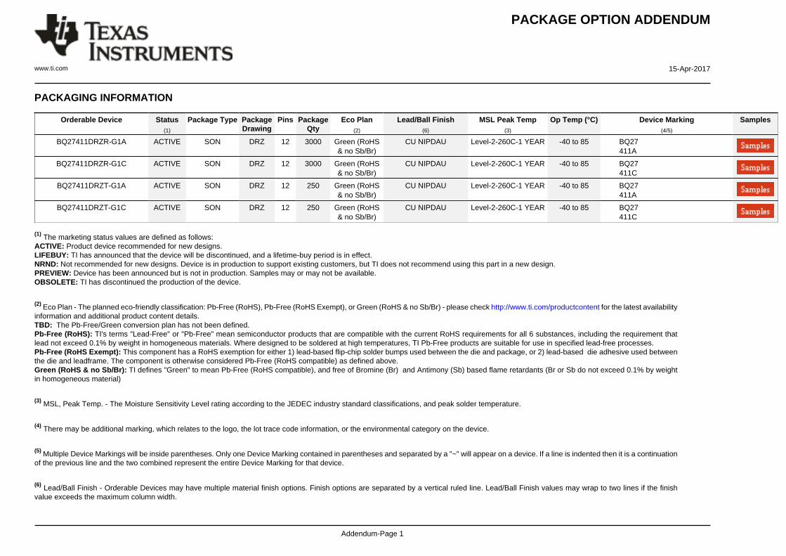
PACKAGING INFORMATION
Orderable Device Status(1)
Package Type PackageDrawing
Pins PackageQty
Eco Plan(2)
Lead/Ball Finish(6)
MSL Peak Temp(3)
Op Temp (°C) Device Marking(4/5)
Samples
BQ27411DRZR-G1A ACTIVE SON DRZ 12 3000 Green (RoHS& no Sb/Br)
CU NIPDAU Level-2-260C-1 YEAR -40 to 85 BQ27411A
BQ27411DRZR-G1C ACTIVE SON DRZ 12 3000 Green (RoHS& no Sb/Br)
CU NIPDAU Level-2-260C-1 YEAR -40 to 85 BQ27411C
BQ27411DRZT-G1A ACTIVE SON DRZ 12 250 Green (RoHS& no Sb/Br)
CU NIPDAU Level-2-260C-1 YEAR -40 to 85 BQ27411A
BQ27411DRZT-G1C ACTIVE SON DRZ 12 250 Green (RoHS& no Sb/Br)
CU NIPDAU Level-2-260C-1 YEAR -40 to 85 BQ27411C
(1) The marketing status values are defined as follows:ACTIVE: Product device recommended for new designs.LIFEBUY: TI has announced that the device will be discontinued, and a lifetime-buy period is in effect.NRND: Not recommended for new designs. Device is in production to support existing customers, but TI does not recommend using this part in a new design.PREVIEW: Device has been announced but is not in production. Samples may or may not be available.OBSOLETE: TI has discontinued the production of the device.
(2) Eco Plan - The planned eco-friendly classification: Pb-Free (RoHS), Pb-Free (RoHS Exempt), or Green (RoHS & no Sb/Br) - please check http://www.ti.com/productcontent for the latest availabilityinformation and additional product content details.TBD: The Pb-Free/Green conversion plan has not been defined.Pb-Free (RoHS): TI's terms "Lead-Free" or "Pb-Free" mean semiconductor products that are compatible with the current RoHS requirements for all 6 substances, including the requirement thatlead not exceed 0.1% by weight in homogeneous materials. Where designed to be soldered at high temperatures, TI Pb-Free products are suitable for use in specified lead-free processes.Pb-Free (RoHS Exempt): This component has a RoHS exemption for either 1) lead-based flip-chip solder bumps used between the die and package, or 2) lead-based die adhesive used betweenthe die and leadframe. The component is otherwise considered Pb-Free (RoHS compatible) as defined above.Green (RoHS & no Sb/Br): TI defines "Green" to mean Pb-Free (RoHS compatible), and free of Bromine (Br) and Antimony (Sb) based flame retardants (Br or Sb do not exceed 0.1% by weightin homogeneous material)
(3) MSL, Peak Temp. - The Moisture Sensitivity Level rating according to the JEDEC industry standard classifications, and peak solder temperature.
(4) There may be additional marking, which relates to the logo, the lot trace code information, or the environmental category on the device.
(5) Multiple Device Markings will be inside parentheses. Only one Device Marking contained in parentheses and separated by a "~" will appear on a device. If a line is indented then it is a continuationof the previous line and the two combined represent the entire Device Marking for that device.
(6) Lead/Ball Finish - Orderable Devices may have multiple material finish options. Finish options are separated by a vertical ruled line. Lead/Ball Finish values may wrap to two lines if the finishvalue exceeds the maximum column width.
PACKAGE OPTION ADDENDUM
www.ti.com 15-Apr-2017
Addendum-Page 2
Important Information and Disclaimer:The information provided on this page represents TI's knowledge and belief as of the date that it is provided. TI bases its knowledge and belief on informationprovided by third parties, and makes no representation or warranty as to the accuracy of such information. Efforts are underway to better integrate information from third parties. TI has taken andcontinues to take reasonable steps to provide representative and accurate information but may not have conducted destructive testing or chemical analysis on incoming materials and chemicals.TI and TI suppliers consider certain information to be proprietary, and thus CAS numbers and other limited information may not be available for release.
In no event shall TI's liability arising out of such information exceed the total purchase price of the TI part(s) at issue in this document sold by TI to Customer on an annual basis.
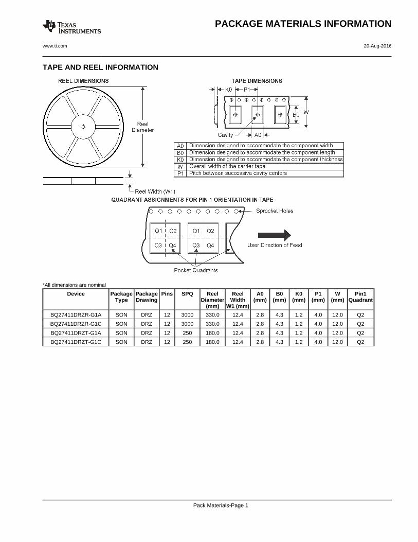
TAPE AND REEL INFORMATION
*All dimensions are nominal
Device PackageType
PackageDrawing
Pins SPQ ReelDiameter
(mm)
ReelWidth
W1 (mm)
A0(mm)
B0(mm)
K0(mm)
P1(mm)
W(mm)
Pin1Quadrant
BQ27411DRZR-G1A SON DRZ 12 3000 330.0 12.4 2.8 4.3 1.2 4.0 12.0 Q2
BQ27411DRZR-G1C SON DRZ 12 3000 330.0 12.4 2.8 4.3 1.2 4.0 12.0 Q2
BQ27411DRZT-G1A SON DRZ 12 250 180.0 12.4 2.8 4.3 1.2 4.0 12.0 Q2
BQ27411DRZT-G1C SON DRZ 12 250 180.0 12.4 2.8 4.3 1.2 4.0 12.0 Q2
PACKAGE MATERIALS INFORMATION
www.ti.com 20-Aug-2016
Pack Materials-Page 1
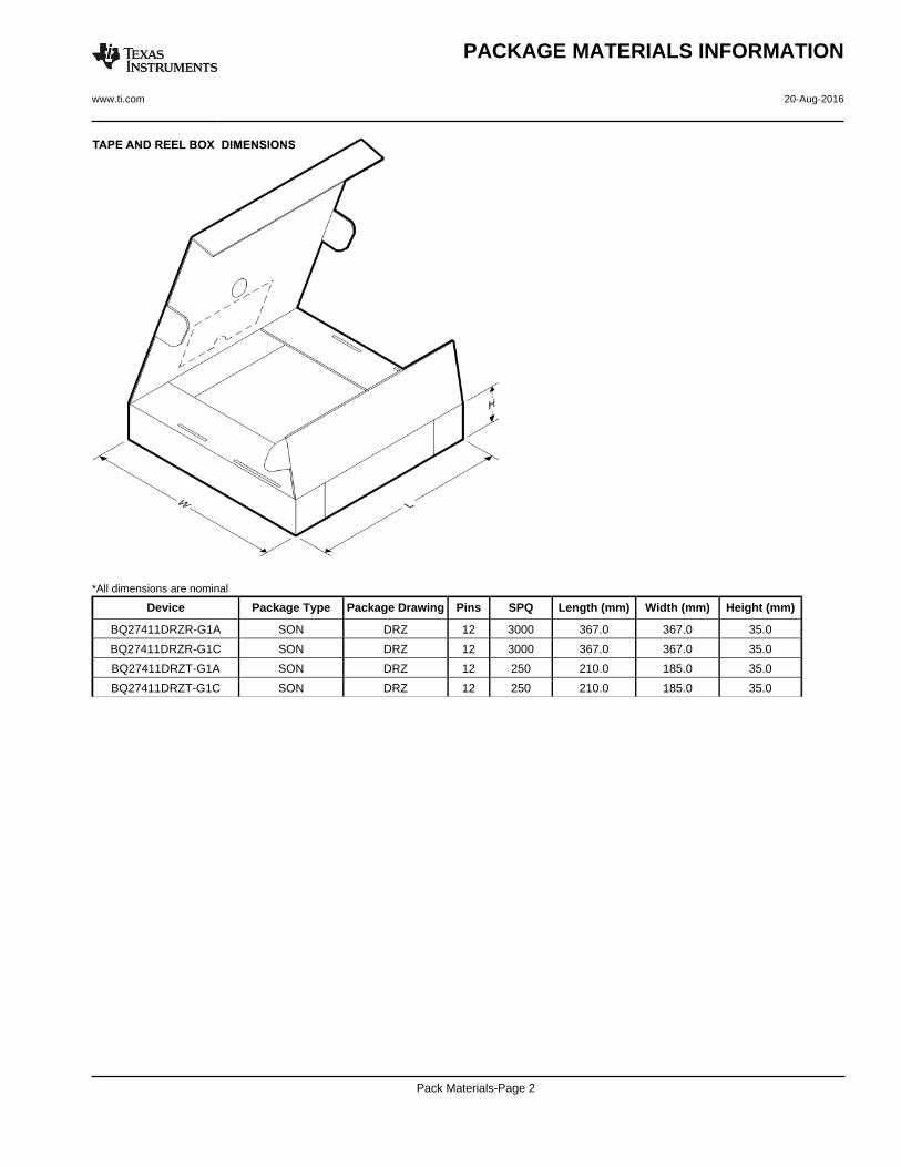
*All dimensions are nominal
Device Package Type Package Drawing Pins SPQ Length (mm) Width (mm) Height (mm)
BQ27411DRZR-G1A SON DRZ 12 3000 367.0 367.0 35.0
BQ27411DRZR-G1C SON DRZ 12 3000 367.0 367.0 35.0
BQ27411DRZT-G1A SON DRZ 12 250 210.0 185.0 35.0
BQ27411DRZT-G1C SON DRZ 12 250 210.0 185.0 35.0
PACKAGE MATERIALS INFORMATION
www.ti.com 20-Aug-2016
Pack Materials-Page 2

IMPORTANT NOTICE
Texas Instruments Incorporated (TI) reserves the right to make corrections, enhancements, improvements and other changes to itssemiconductor products and services per JESD46, latest issue, and to discontinue any product or service per JESD48, latest issue. Buyersshould obtain the latest relevant information before placing orders and should verify that such information is current and complete.TI’s published terms of sale for semiconductor products (http://www.ti.com/sc/docs/stdterms.htm) apply to the sale of packaged integratedcircuit products that TI has qualified and released to market. Additional terms may apply to the use or sale of other types of TI products andservices.Reproduction of significant portions of TI information in TI data sheets is permissible only if reproduction is without alteration and isaccompanied by all associated warranties, conditions, limitations, and notices. TI is not responsible or liable for such reproduceddocumentation. Information of third parties may be subject to additional restrictions. Resale of TI products or services with statementsdifferent from or beyond the parameters stated by TI for that product or service voids all express and any implied warranties for theassociated TI product or service and is an unfair and deceptive business practice. TI is not responsible or liable for any such statements.Buyers and others who are developing systems that incorporate TI products (collectively, “Designers”) understand and agree that Designersremain responsible for using their independent analysis, evaluation and judgment in designing their applications and that Designers havefull and exclusive responsibility to assure the safety of Designers' applications and compliance of their applications (and of all TI productsused in or for Designers’ applications) with all applicable regulations, laws and other applicable requirements. Designer represents that, withrespect to their applications, Designer has all the necessary expertise to create and implement safeguards that (1) anticipate dangerousconsequences of failures, (2) monitor failures and their consequences, and (3) lessen the likelihood of failures that might cause harm andtake appropriate actions. Designer agrees that prior to using or distributing any applications that include TI products, Designer willthoroughly test such applications and the functionality of such TI products as used in such applications.TI’s provision of technical, application or other design advice, quality characterization, reliability data or other services or information,including, but not limited to, reference designs and materials relating to evaluation modules, (collectively, “TI Resources”) are intended toassist designers who are developing applications that incorporate TI products; by downloading, accessing or using TI Resources in anyway, Designer (individually or, if Designer is acting on behalf of a company, Designer’s company) agrees to use any particular TI Resourcesolely for this purpose and subject to the terms of this Notice.TI’s provision of TI Resources does not expand or otherwise alter TI’s applicable published warranties or warranty disclaimers for TIproducts, and no additional obligations or liabilities arise from TI providing such TI Resources. TI reserves the right to make corrections,enhancements, improvements and other changes to its TI Resources. TI has not conducted any testing other than that specificallydescribed in the published documentation for a particular TI Resource.Designer is authorized to use, copy and modify any individual TI Resource only in connection with the development of applications thatinclude the TI product(s) identified in such TI Resource. NO OTHER LICENSE, EXPRESS OR IMPLIED, BY ESTOPPEL OR OTHERWISETO ANY OTHER TI INTELLECTUAL PROPERTY RIGHT, AND NO LICENSE TO ANY TECHNOLOGY OR INTELLECTUAL PROPERTYRIGHT OF TI OR ANY THIRD PARTY IS GRANTED HEREIN, including but not limited to any patent right, copyright, mask work right, orother intellectual property right relating to any combination, machine, or process in which TI products or services are used. Informationregarding or referencing third-party products or services does not constitute a license to use such products or services, or a warranty orendorsement thereof. Use of TI Resources may require a license from a third party under the patents or other intellectual property of thethird party, or a license from TI under the patents or other intellectual property of TI.TI RESOURCES ARE PROVIDED “AS IS” AND WITH ALL FAULTS. TI DISCLAIMS ALL OTHER WARRANTIES ORREPRESENTATIONS, EXPRESS OR IMPLIED, REGARDING RESOURCES OR USE THEREOF, INCLUDING BUT NOT LIMITED TOACCURACY OR COMPLETENESS, TITLE, ANY EPIDEMIC FAILURE WARRANTY AND ANY IMPLIED WARRANTIES OFMERCHANTABILITY, FITNESS FOR A PARTICULAR PURPOSE, AND NON-INFRINGEMENT OF ANY THIRD PARTY INTELLECTUALPROPERTY RIGHTS. TI SHALL NOT BE LIABLE FOR AND SHALL NOT DEFEND OR INDEMNIFY DESIGNER AGAINST ANY CLAIM,INCLUDING BUT NOT LIMITED TO ANY INFRINGEMENT CLAIM THAT RELATES TO OR IS BASED ON ANY COMBINATION OFPRODUCTS EVEN IF DESCRIBED IN TI RESOURCES OR OTHERWISE. IN NO EVENT SHALL TI BE LIABLE FOR ANY ACTUAL,DIRECT, SPECIAL, COLLATERAL, INDIRECT, PUNITIVE, INCIDENTAL, CONSEQUENTIAL OR EXEMPLARY DAMAGES INCONNECTION WITH OR ARISING OUT OF TI RESOURCES OR USE THEREOF, AND REGARDLESS OF WHETHER TI HAS BEENADVISED OF THE POSSIBILITY OF SUCH DAMAGES.Unless TI has explicitly designated an individual product as meeting the requirements of a particular industry standard (e.g., ISO/TS 16949and ISO 26262), TI is not responsible for any failure to meet such industry standard requirements.Where TI specifically promotes products as facilitating functional safety or as compliant with industry functional safety standards, suchproducts are intended to help enable customers to design and create their own applications that meet applicable functional safety standardsand requirements. Using products in an application does not by itself establish any safety features in the application. Designers mustensure compliance with safety-related requirements and standards applicable to their applications. Designer may not use any TI products inlife-critical medical equipment unless authorized officers of the parties have executed a special contract specifically governing such use.Life-critical medical equipment is medical equipment where failure of such equipment would cause serious bodily injury or death (e.g., lifesupport, pacemakers, defibrillators, heart pumps, neurostimulators, and implantables). Such equipment includes, without limitation, allmedical devices identified by the U.S. Food and Drug Administration as Class III devices and equivalent classifications outside the U.S.TI may expressly designate certain products as completing a particular qualification (e.g., Q100, Military Grade, or Enhanced Product).Designers agree that it has the necessary expertise to select the product with the appropriate qualification designation for their applicationsand that proper product selection is at Designers’ own risk. Designers are solely responsible for compliance with all legal and regulatoryrequirements in connection with such selection.Designer will fully indemnify TI and its representatives against any damages, costs, losses, and/or liabilities arising out of Designer’s non-compliance with the terms and provisions of this Notice.
Mailing Address: Texas Instruments, Post Office Box 655303, Dallas, Texas 75265Copyright © 2017, Texas Instruments Incorporated