Embed Size (px)
Citation preview
1SLUUBK9–September 2017Submit Documentation Feedback
Copyright © 2017, Texas Instruments Incorporated
bq25600, bq25600D PWR771 Evaluation Module
User's GuideSLUUBK9–September 2017
bq25600, bq25600D PWR771 Evaluation Module
This user's guide provides detailed testing instructions for the bq25600 and bq25600D evaluation modules(EVM). Also included are descriptions of the necessary equipment, equipment setup, and procedures. Thereference documentation contains the printed-circuit board layouts, schematics, and the bill of materials(BOM).
Contents1 Introduction ................................................................................................................... 2
1.1 EVM Features ....................................................................................................... 21.2 I/O Descriptions ..................................................................................................... 2
2 Test Summary................................................................................................................ 42.1 Equipment ........................................................................................................... 42.2 Equipment Setup.................................................................................................... 42.3 Test Procedure...................................................................................................... 6
3 PCB Layout Guideline....................................................................................................... 74 Board Layout, Schematic, and Bill of Materials.......................................................................... 7
4.1 Schematic............................................................................................................ 74.2 Bill of Materials .................................................................................................... 10
List of Figures
1 Connections of the EV2300/2400 Kit ..................................................................................... 42 Original Test Setup for bq25600xEVM.................................................................................... 53 Selection Window of bqStudio Evaluation Software .................................................................... 54 Schematic for bq25600 EVM............................................................................................... 85 Schematic for bq25600D EVM ............................................................................................. 9
List of Tables
1 Device Data Sheets ......................................................................................................... 22 PWR771 EVM Connections ................................................................................................ 23 EVM Jumper Connections and Shunt Installation ....................................................................... 34 Recommended Operating Conditions..................................................................................... 35 bq25600EVM-771 Bill of Materials....................................................................................... 106 bq25600DEVM-771 Bill of Materials ..................................................................................... 14
TrademarksAll trademarks are the property of their respective owners.
Introduction www.ti.com
2 SLUUBK9–September 2017Submit Documentation Feedback
Copyright © 2017, Texas Instruments Incorporated
bq25600, bq25600D PWR771 Evaluation Module
1 Introduction
1.1 EVM FeaturesFor detailed features and operation, see Table 1 for a list of devices and their data sheets.
Table 1. Device Data Sheets
Device Data Sheet EVM Label Variantbq25600 SLUSCJ4 bq25600EVM-771 003
bq25600D SLUSCJ4 bq25600DEVM-771 004
The bq25600(D) evaluation module (EVM) is a complete charger module for evaluating an I2C-controlledsingle NVDC-1 charge using the bq25600(D) device.
This EVM does not include the USB-to-GPIO or EV2300/EV2400 interface board. To evaluate the EVM, aUSB-to-GPIO interface board must be ordered separately.
1.2 I/O DescriptionsTable 2 lists the jumper connections available on this EVM.
Table 2. PWR771 EVM Connections
Jack DescriptionJ1-VAC Input: positive terminalJ1-GND Input: negative terminal (ground terminal)J2-PMID PMID pin connection, power bank outputJ2-GND Ground and power bank output negative terminal
J3 Output mini-USB portJ4-SYS Connected to systemJ4-GND GroundJ5-BAT Connected to battery pack
J5-BATSNS Connected to battery pack for voltage sensingJ5-GND Ground
J6 I2C 4-pin connectorJ7 USB-TO-GPIO connector
www.ti.com Introduction
3SLUUBK9–September 2017Submit Documentation Feedback
Copyright © 2017, Texas Instruments Incorporated
bq25600, bq25600D PWR771 Evaluation Module
Table 3 lists the EVM jumper connections.
Table 3. EVM Jumper Connections and Shunt Installation
Jack Description bq25600 Setting bq25600D SettingJP1 D+ and PSEL pin selection Short PSEL to low Not installedJP2 CE pin setting: pull low to enable the charge Installed InstalledJP3 SCL and OTG pin setting Not installed Not installedJP4 STAT, PG, CE, INT, OTG pins internal pullup source (VSYS
or BAT)Short to VSYS Short to VSYS
JP5 TS pin to GND Not installed Not installedJP6 TS resistor divider pullup source (REGN) connection Installed InstalledJP7 Internal 10 k to GND to TS pin Installed InstalledJP8 BATSNS selection Short to BAT Short to BATJP9 QON and VSET pin setting Not installed Not installedJP10 STAT pin setting Installed InstalledJP12 SDA and PG pin setting Installed Not installedJP13 D+ and PSEL to J3 Not installed InstalledJP14 D- and PG to J3 Not installed InstalledJP15 D- and PG pin setting Installed Not installedJP100 Add 1-µF (C100) VBUS capacitor Not installed Not installedJP101 Add 10-µF (C101) PMID capacitor Not installed Not installedJP103 Add 10-µF (C103) SYS capacitor Not installed Not installedJP104 Add 4.7-µF (C104) BAT capacitor Not installed Not installed
S1 QON control Default off Default offS2 Switch to short indicator LEDs Default off Default off
Table 4 lists the recommended operating conditions for this EVM.
Table 4. Recommended Operating Conditions
Symbol Description MIN TYP MAX UNITSupply voltage, VVBUS Input voltage from AC adapter 3.9 5 14 VBattery voltage, VBAT Voltage applied at VBAT terminal 0 4.208 4.624 VIBAT Fast charging current 0 2.5 AIBATOP Discharging current through
internal MOSFET0 6 A
Supply current, IIN Maximum input current from ACadapter input
0 3.25 A
To Computer USB Port
4-PinCable to
EVM
I 2C
EV
2300/2400
Texas Instrum
ents
US
B
Test Summary www.ti.com
4 SLUUBK9–September 2017Submit Documentation Feedback
Copyright © 2017, Texas Instruments Incorporated
bq25600, bq25600D PWR771 Evaluation Module
2 Test Summary
2.1 EquipmentThis section includes a list of supplies required for testing this EVM.• Power supply: Power supply #1 (PS#1): A power supply capable of supplying 5 V at 1 A is required.
While this part can handle larger voltage and current, it is not necessary for this procedure.• Load #1:
– 4-quadrant supply, constant voltage < 4.5 V, A 0 – 20 V, 0 – 5 A, > 30-W system, DC electronicload and setting as constant voltage load modeor
– Kepco load: BOP 20 – 5M, DC 0 to ±20 V, 0 to ±5 A (or higher).• Load #2: Use with Boost Mode, PMID to GND load, 10 Ω, 5 W or greater.• Meters:
– Six Fluke 75 multimeters, (equivalent or better)or
– Four equivalent voltage meters and two equivalent current meters. The current meters must becapable of measuring 5-A current.
• Computer: A computer with at least one USB port and a USB cable. The bq25600DEVM evaluationsoftware must be properly installed.
• USB-to-GPIO Communication Kit: EV2300/EV2400 USB-based PC interface board.• Software: Download bqStudio from www.ti.com.
1. Double click the Battery Management Studio-1.3.20_Build2-Setup installation file, follow theinstallation steps. The software supports the Microsoft® Windows® XP and Windows 7 operatingsystems.
2. Copy the bq25600 bqz file to C:\ti\BatteryManagementStudio\config
2.2 Equipment SetupUse the following instructions to set up the equipment:1. Set PS#1 for 5-V DC, 1-A current limit and then turn off the supply.2. Connect the output of PS#1 in series with a current meter (multimeter) to J1 (VBUS and GND).3. Connect a voltage meter across TP1 (VBUS) and TP18 (GND).4. Turn on the load, set it to constant voltage mode and set the output to 2.5 V.5. Turn off (disable) the load.6. Connect the load to J5 (BAT and GND), as shown in Figure 2.7. Connect one voltage meter across TP9 (BAT) and TP20 (GND) to measure the battery voltage and
another voltage meter across TP28 and TP29 to measure the battery current sensing resistor voltage.The sensing resistor is 10 mΩ. It is also OK to use the optional current meter in series to measure thebattery current.
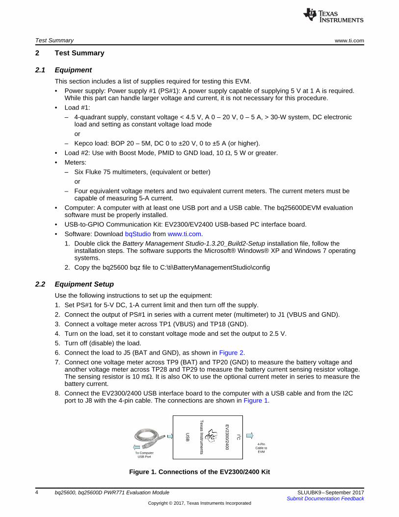
8. Connect the EV2300/2400 USB interface board to the computer with a USB cable and from the I2Cport to J8 with the 4-pin cable. The connections are shown in Figure 1.
Figure 1. Connections of the EV2300/2400 Kit
Copyright © 2017, Texas Instruments Incorporated
www.ti.com Test Summary
5SLUUBK9–September 2017Submit Documentation Feedback
Copyright © 2017, Texas Instruments Incorporated
bq25600, bq25600D PWR771 Evaluation Module
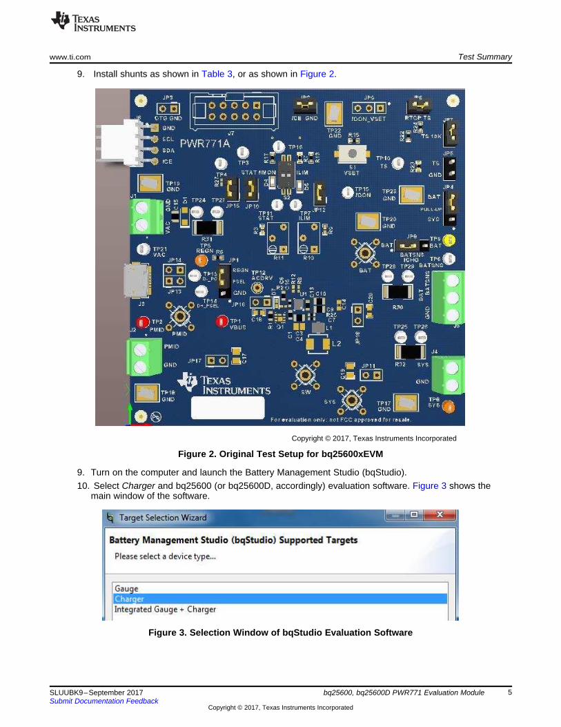
9. Install shunts as shown in Table 3, or as shown in Figure 2.
Figure 2. Original Test Setup for bq25600xEVM
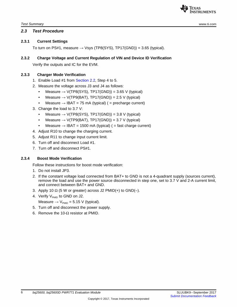
9. Turn on the computer and launch the Battery Management Studio (bqStudio).10. Select Charger and bq25600 (or bq25600D, accordingly) evaluation software. Figure 3 shows the
main window of the software.
Figure 3. Selection Window of bqStudio Evaluation Software
Test Summary www.ti.com
6 SLUUBK9–September 2017Submit Documentation Feedback
Copyright © 2017, Texas Instruments Incorporated
bq25600, bq25600D PWR771 Evaluation Module
2.3 Test Procedure
2.3.1 Current SettingsTo turn on PS#1, measure → Vsys (TP8(SYS), TP17(GND)) = 3.65 (typical).
2.3.2 Charge Voltage and Current Regulation of VIN and Device ID VerificationVerify the outputs and IC for the EVM.
2.3.3 Charger Mode Verification1. Enable Load #1 from Section 2.2, Step 4 to 5.2. Measure the voltage across J3 and J4 as follows:
• Measure → V(TP8(SYS), TP17(GND)) = 3.65 V (typical)• Measure → V(TP9(BAT), TP17(GND)) = 2.5 V (typical)• Measure → IBAT = 75 mA (typical) ( = precharge current)
3. Change the load to 3.7 V:• Measure → V(TP8(SYS), TP17(GND)) = 3.8 V (typical)• Measure → V(TP9(BAT), TP17(GND)) = 3.7 V (typical)• Measure → IBAT = 1500 mA (typical) ( = fast charge current)
4. Adjust R10 to change the charging current.5. Adjust R11 to change input current limit.6. Turn off and disconnect Load #1.7. Turn off and disconnect PS#1.
2.3.4 Boost Mode VerificationFollow these instructions for boost mode verification:1. Do not install JP3.2. If the constant voltage load connected from BAT+ to GND is not a 4-quadrant supply (sources current),
remove the load and use the power source disconnected in step one, set to 3.7 V and 2-A current limit,and connect between BAT+ and GND.
3. Apply 10 Ω (5 W or greater) across J2 PMID(+) to GND(–).4. Verify VPMID to GND on J2.
Measure → VPMID = 5.15 V (typical).5. Turn off and disconnect the power supply.6. Remove the 10-Ω resistor at PMID.

www.ti.com PCB Layout Guideline
7SLUUBK9–September 2017Submit Documentation Feedback
Copyright © 2017, Texas Instruments Incorporated
bq25600, bq25600D PWR771 Evaluation Module
2.3.5 Helpful Tips• The leads and cables to the various power supplies, batteries and loads have resistance. The current
meters also have series resistance. The charger dynamically reduces charge current depending on thevoltage sensed at its VBUS pin (using the VINDPM feature), BAT pin (as part of normal termination),and TS pin (through its battery temperature monitoring feature via battery thermistor). Therefore,voltmeters must be used to measure the voltage as close to the IC pins as possible instead of relyingon the digital readouts of the power supply. If a battery thermistor is not available, make sure shuntsJP9 and JP10 are in place.
• When using a source meter that can source and sink current as your battery simulator, TI highlyrecommends adding a large (1000+ μF) capacitor at the EVM BAT and GND connectors in order toprevent oscillations at the BAT pin due to mismatched impedances of the charger output and sourcemeter input within their respective regulation loop bandwidths. Configuring the source meter for 4-wiresensing eliminates the need for a separate voltmeter to measure the voltage at the BAT pin. Whenusing 4-wire sensing, always ensure that the sensing leads are connected in order to preventaccidental overvoltage by the power leads.
• For precise measurements of charge current and battery regulation near termination, the current meterin series with the battery or battery simulator should not be set to auto-range and may need beremoved entirely. An alternate method for measuring charge current is to either use an oscilloscopewith hall effect current probe or place a 1% or better, thermally capable (for example, 0.010 Ω in 1210or larger footprint) resistor in series between the BAT pin and battery and measure the voltage acrossthat resistor.
3 PCB Layout GuidelineMinimize the switching node rise and fall times for minimum switching loss. Proper layout of thecomponents minimizing high-frequency current path loop is important to prevent electrical and magneticfield radiation and high-frequency resonant problems. This PCB layout priority list must be followed in theorder presented for proper layout:1. Place the input capacitor as close as possible to the PMID pin and GND pin connections and use the
shortest copper trace connection or GND plane.2. Put an output capacitor near to the inductor and the IC.3. Decoupling capacitors should be placed next to the IC pins and make the trace connection as short as
possible.4. Place the inductor input terminal and SW pin as close as possible. Minimize the copper area of this
trace to lower electrical and magnetic field radiation but make the trace is wide enough to carry thecharging current. Do not use multiple layers in parallel for this connection. Minimize parasiticcapacitance from this area to any other trace or plane.
5. It is OK to connect all grounds together to reduce PCB size and improve thermal dissipation.6. Try to avoid ground planes in parallel with high frequency traces in other layers
See the EVM design for the recommended component placement with trace and via locations.
4 Board Layout, Schematic, and Bill of Materials
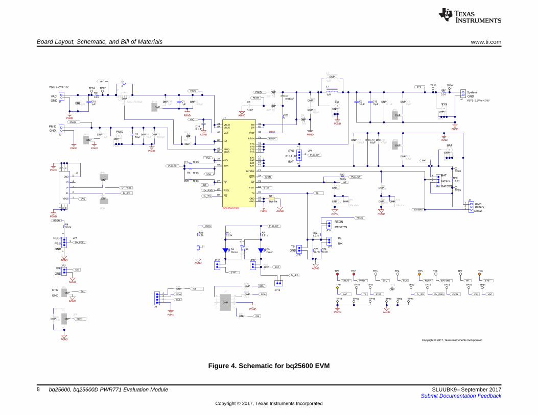
4.1 SchematicFigure 4 shows the schematic for the bq25600 EVM.
1 2
3 4
5 6
7 8
9 10
J7
DNP
0
R21DNP
200
R19DNP
200
R20DNP SDA
SCL
PGND
VBUS1
D-2
D+3
ID4
GND5
678
11
109
J3
VAC
PGND
PGND
4
1
2
3
J6
PGND
SCL
SDA
/CE
D-_/PG
D+_PSEL
PGND
VBUS
VAC
GND
PMID
GND
Vbus: 3.9V to 14V
1000pFC2DNP
PGND
10.0kR4
10.0kR5
JP3
DNP
/CE
AGND
AGND
TP2TP1
1µFC1
TP3 TP4 TP7
J113VD1
DNP
2.21kR17
30.1kR23
10R26
DNP
0.1µFC11DNP
System
GND
GND
PGND
Battery
PGND
PULL-UP
TS
GND
10µFC9
10µFC10
10µFC19DNP
20V D3
DNP
VSYS: 3.5V to 4.75V
AGND
40V D2
DNP
0.047µFC7
0R25
1
2
3
J5
TP6
PGND
1µH
L1
4.7kR15
AGND
S1
STAT
REGN
3
5,6,8 4,71,2,
Q1
CSD17313Q2
DNP
0R2
DNP
PGND
JP16
DNP
JP17
DNP
PGNDPGND
1µFC18DNP
SCL
SDA
VBUS PMID
VAC
VAC
SDA
D+_PSEL
D-_/PG
10k ohm
R10DNP
221R8
DNP
2.80kR9
DNP
PGND
/CE
10K
TS
20V
D6
DNP
J2
1
2
3
JP1
AGND
10.0kR6
REGN
D+_PSEL
JP2
/CE
AGND
PMID
10µFC3
10µFC17DNP
10µFC4DNP
1000pFC5DNP
4.7µF
C6
AGND
PMID
/QON
/QON
JP5
10.0kR24
5.23kR22
JP6
REGN
JP7
REGN
110pFC8DNP
INT
AGND
SW
DNP
PGND
1
2
3
JP4
PULL-UP
JP18
DNP
JP11
DNP
1000pFC12DNP
10µFC13
4.7µFC20DNP
4.7µFC14DNP
1
2
3
JP8
NT1
Net-Tie
0
R16DNP
GreenD4
REGN
RTOP TS
BATSNS
BAT
PSEL
GND
REGN
/CE
GND
GND
OTG
TP9
TP8
SYS
BAT
BAT
SYS
TP5
REGN BATSNS INTSCL
TP10 TP11
TS
TS
TP12
DNP
TP13
D-_/PG
TP14 TP15
/QOND+_PSEL
TP16
/CE
TP17 TP18 TP19 TP20
AGNDPGND
BAT
SYS
PULLUP
158R12
DNP
AGND
10k ohm
R11DNP1.00k
R3DNP
PULL-UP
SYS
DNP
BAT
DNP
PMID
DNP
BAT
SYSSW
PMID
JP13
DNP
SCL
1
2
3
JP9
DNP
AGND
/QON
1µFC15
0.1µFC16
AGND
0
R1
STAT
STAT
BATSNS
J4
BTST
JP10
2.21kR7
GreenD5
JP12
SDA
TP21
VAC
0
R27DNP
D-_/PG
10.0kR29
DNP
12
JP14
DNP
JP15
10.0k
R13PULL-UP
GNDA1
GNDB1
REGNC4
SYSC2
BATC1
SWA2
SWB2
BTSTC3
SYSD2
BATD1
PMIDB3
PMIDA3
STATE5
SYSE2
BATE1
VBUSA4
VBUSB4
INTF4
SYSF2
BATF1
NCB5
SCLF5
SDAE4
PSELC5
BATSNSF3
VACA5
TSD3
QOND4
PGD5
CEE3
U1
BQ25600YFFR
1 2
4 3
S2
10.0kR28
TP22 TP23
0.01
R30
0.01
R31
D7
DNP
BATCON
0.01
R32TP24 TP27
TP25 TP26
TP28
TP29
1µH
L2
DNP
BATSNS
Copyright © 2017, Texas Instruments Incorporated
Board Layout, Schematic, and Bill of Materials www.ti.com
8 SLUUBK9–September 2017Submit Documentation Feedback
Copyright © 2017, Texas Instruments Incorporated
bq25600, bq25600D PWR771 Evaluation Module
Figure 4. Schematic for bq25600 EVM
1 2
3 4
5 6
7 8
9 10
J7
DNP
0
R21DNP
200
R19DNP
200
R20DNP SDA
SCL
PGND
VBUS1
D-2
D+3
ID4
GND5
678
11
109
J3
VAC
PGND
PGND
4
1
2
3
J6
PGND
SCL
SDA
/CE
D-_/PG
D+_PSEL
PGND
VBUS
VAC
GND
PMID
GND
Vbus: 3.9V to 14V
1000pFC2DNP
PGND
10.0kR4
10.0kR5
JP3
DNP
/CE
AGND
AGND
TP2TP1
1µFC1
TP3 TP4 TP7
J113VD1
DNP
2.21kR17
30.1kR23
10R26
DNP
0.1µFC11DNP
System
GND
GND
PGND
Battery
PGND
PULL-UP
TS
GND
10µFC9
10µFC10
10µFC19DNP
20V D3
DNP
VSYS: 3.5V to 4.75V
AGND
40V D2
DNP
0.047µFC7
0R25
1
2
3
J5
TP6
PGND
1µH
L1
4.7kR15
AGND
S1
STAT
REGN
3
5,6,8 4,71,2,
Q1
CSD17313Q2
DNP
0R2
DNP
PGND
JP16
DNP
JP17
DNP
PGNDPGND
1µFC18DNP
SCL
SDA
VBUS PMID
VAC
VAC
SDA
D+_PSEL
D-_/PG
10k ohm
R10DNP
221R8
DNP
2.80kR9
DNP
PGND
/CE
10K
TS
20V
D6
DNP
J2
1
2
3
JP1
DNP
AGND
10.0kR6
REGN
D+_PSEL
JP2
/CE
AGND
PMID
10µFC3
10µFC17DNP
10µFC4DNP
1000pFC5DNP
4.7µF
C6
AGND
PMID
/QON
/QON
JP5
10.0kR24
5.23kR22
JP6
REGN
JP7
REGN
110pFC8DNP
INT
AGND
SW
DNP
PGND
1
2
3
JP4
PULL-UP
JP18
DNP
JP11
DNP
1000pFC12DNP
10µFC13
4.7µFC20DNP
4.7µFC14DNP
1
2
3
JP8
NT1
Net-Tie
0
R16DNP
GreenD4
REGN
RTOP TS
BATSNS
BAT
PSEL
GND
REGN
/CE
GND
GND
OTG
TP9
TP8
SYS
BAT
BAT
SYS
TP5
REGN BATSNS INTSCL
TP10 TP11
TS
TS
TP12
DNP
TP13
D-_/PG
TP14 TP15
/QOND+_PSEL
TP16
/CE
TP17 TP18 TP19 TP20
AGNDPGND
BAT
SYS
PULLUP
158R12
DNP
AGND
10k ohm
R11DNP1.00k
R3DNP
PULL-UP
SYS
DNP
BAT
DNP
PMID
DNP
BAT
SYSSW
PMID
JP13
SCL
1
2
3
JP9
DNP
AGND
/QON
1µFC15
0.1µFC16
AGND
0
R1
STAT
STAT
BATSNS
J4
BTST
JP10
2.21kR7
GreenD5
JP12
SDA
TP21
VAC
0
R27DNP
D-_/PG
10.0kR29
12
JP14
JP15
DNP
10.0k
R13PULL-UP
GNDA1
GNDB1
REGNC4
SYSC2
BATC1
SWA2
SWB2
BTSTC3
SYSD2
BATD1
PMIDB3
PMIDA3
STATE5
SYSE2
BATE1
VBUSA4
VBUSB4
INTF4
SYSF2
BATF1
NCB5
SCLF5
SDAE4
D+C5
BATSNSF3
VACA5
TSD3
QOND4
D-D5
CEE3
U1
BQ25600DYFFR
1 2
4 3
S2
10.0kR28
TP22 TP23
0.01
R30
0.01
R31
D7
DNP
BATCON
0.01
R32TP24 TP27
TP25 TP26
TP28
TP29
1µH
L2
DNP
BATSNS
Copyright © 2017, Texas Instruments Incorporated
www.ti.com Board Layout, Schematic, and Bill of Materials
9SLUUBK9–September 2017Submit Documentation Feedback
Copyright © 2017, Texas Instruments Incorporated
bq25600, bq25600D PWR771 Evaluation Module
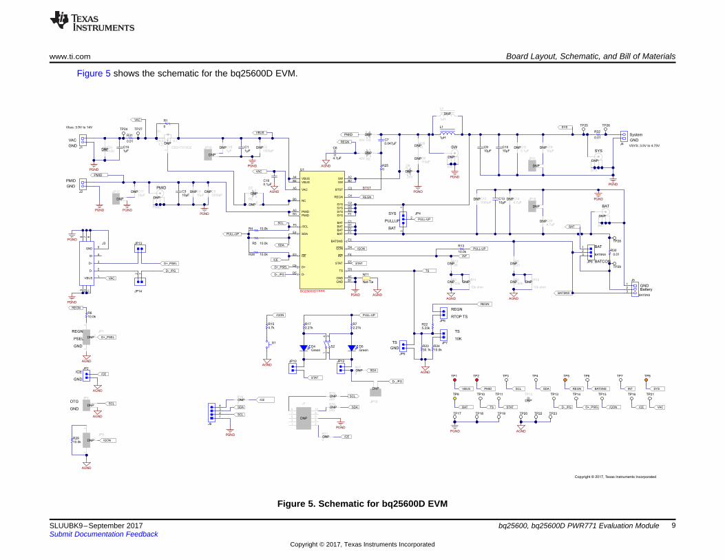
Figure 5 shows the schematic for the bq25600D EVM.
Figure 5. Schematic for bq25600D EVM
Board Layout, Schematic, and Bill of Materials www.ti.com
10 SLUUBK9–September 2017Submit Documentation Feedback
Copyright © 2017, Texas Instruments Incorporated
bq25600, bq25600D PWR771 Evaluation Module
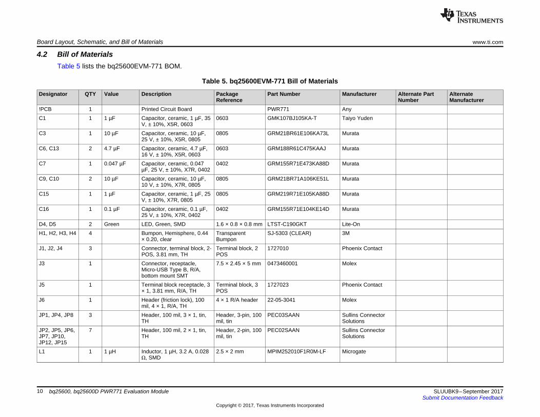
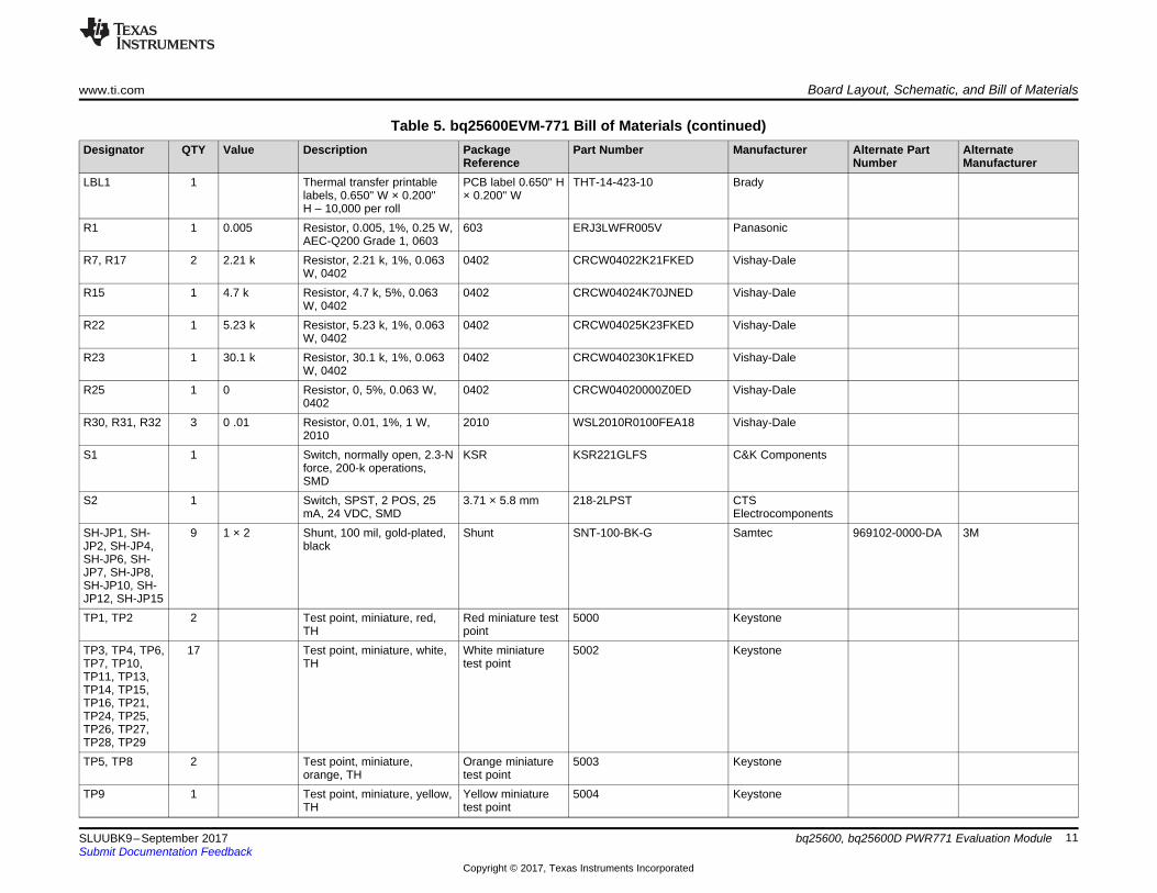
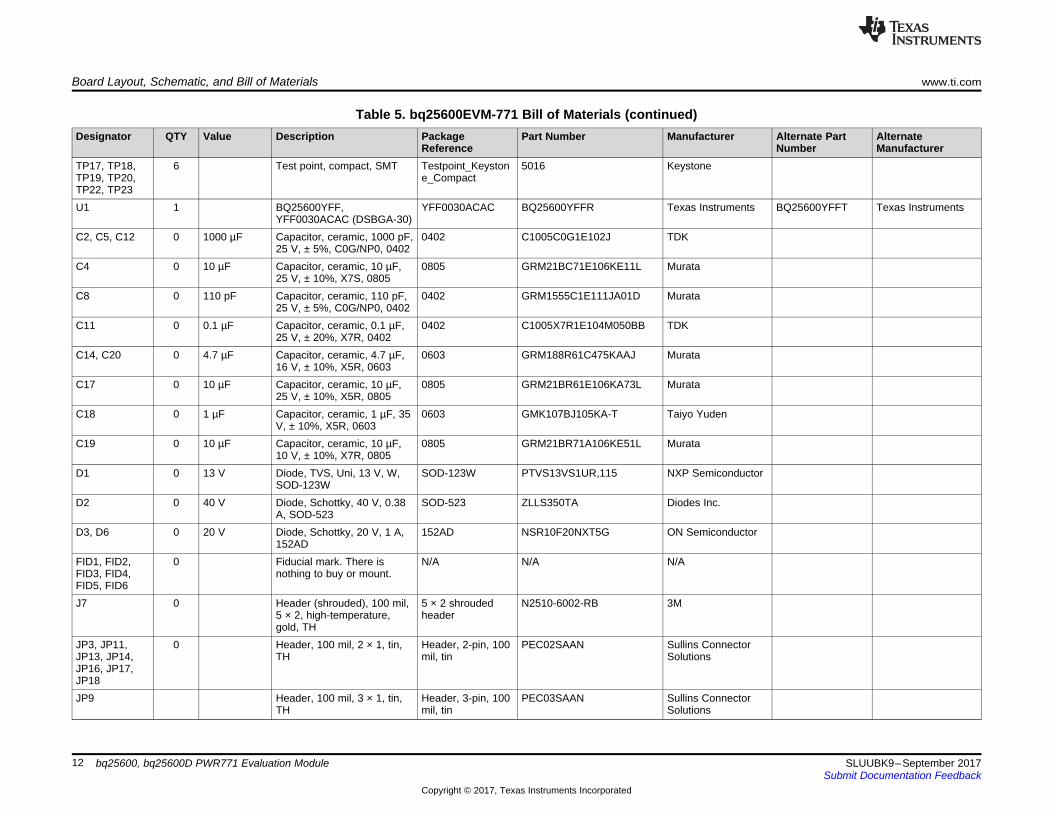
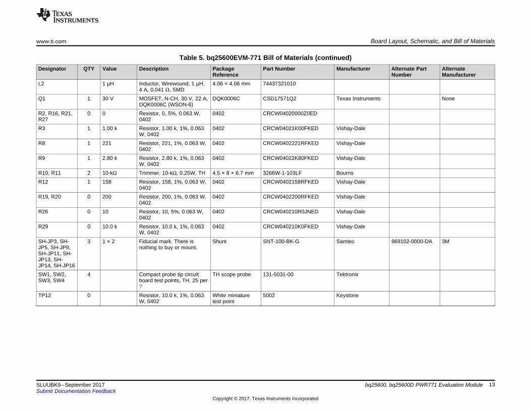
4.2 Bill of MaterialsTable 5 lists the bq25600EVM-771 BOM.
Table 5. bq25600EVM-771 Bill of Materials
Designator QTY Value Description PackageReference
Part Number Manufacturer Alternate PartNumber
AlternateManufacturer
!PCB 1 Printed Circuit Board PWR771 AnyC1 1 1 µF Capacitor, ceramic, 1 µF, 35
V, ± 10%, X5R, 06030603 GMK107BJ105KA-T Taiyo Yuden
C3 1 10 µF Capacitor, ceramic, 10 µF,25 V, ± 10%, X5R, 0805
0805 GRM21BR61E106KA73L Murata
C6, C13 2 4.7 µF Capacitor, ceramic, 4.7 µF,16 V, ± 10%, X5R, 0603
0603 GRM188R61C475KAAJ Murata
C7 1 0.047 µF Capacitor, ceramic, 0.047µF, 25 V, ± 10%, X7R, 0402
0402 GRM155R71E473KA88D Murata
C9, C10 2 10 µF Capacitor, ceramic, 10 µF,10 V, ± 10%, X7R, 0805
0805 GRM21BR71A106KE51L Murata
C15 1 1 µF Capacitor, ceramic, 1 µF, 25V, ± 10%, X7R, 0805
0805 GRM219R71E105KA88D Murata
C16 1 0.1 µF Capacitor, ceramic, 0.1 µF,25 V, ± 10%, X7R, 0402
0402 GRM155R71E104KE14D Murata
D4, D5 2 Green LED, Green, SMD 1.6 × 0.8 × 0.8 mm LTST-C190GKT Lite-OnH1, H2, H3, H4 4 Bumpon, Hemisphere, 0.44
× 0.20, clearTransparentBumpon
SJ-5303 (CLEAR) 3M
J1, J2, J4 3 Connector, terminal block, 2-POS, 3.81 mm, TH
Terminal block, 2POS
1727010 Phoenix Contact
J3 1 Connector, receptacle,Micro-USB Type B, R/A,bottom mount SMT
7.5 × 2.45 × 5 mm 0473460001 Molex
J5 1 Terminal block receptacle, 3× 1, 3.81 mm, R/A, TH
Terminal block, 3POS
1727023 Phoenix Contact
J6 1 Header (friction lock), 100mil, 4 × 1, R/A, TH
4 × 1 R/A header 22-05-3041 Molex
JP1, JP4, JP8 3 Header, 100 mil, 3 × 1, tin,TH
Header, 3-pin, 100mil, tin
PEC03SAAN Sullins ConnectorSolutions
JP2, JP5, JP6,JP7, JP10,JP12, JP15
7 Header, 100 mil, 2 × 1, tin,TH
Header, 2-pin, 100mil, tin
PEC02SAAN Sullins ConnectorSolutions
L1 1 1 µH Inductor, 1 µH, 3.2 A, 0.028Ω, SMD
2.5 × 2 mm MPIM252010F1R0M-LF Microgate
www.ti.com Board Layout, Schematic, and Bill of Materials
11SLUUBK9–September 2017Submit Documentation Feedback
Copyright © 2017, Texas Instruments Incorporated
bq25600, bq25600D PWR771 Evaluation Module
Table 5. bq25600EVM-771 Bill of Materials (continued)Designator QTY Value Description Package
ReferencePart Number Manufacturer Alternate Part
NumberAlternateManufacturer
LBL1 1 Thermal transfer printablelabels, 0.650" W × 0.200"H – 10,000 per roll
PCB label 0.650" H× 0.200" W
THT-14-423-10 Brady
R1 1 0.005 Resistor, 0.005, 1%, 0.25 W,AEC-Q200 Grade 1, 0603
603 ERJ3LWFR005V Panasonic
R7, R17 2 2.21 k Resistor, 2.21 k, 1%, 0.063W, 0402
0402 CRCW04022K21FKED Vishay-Dale
R15 1 4.7 k Resistor, 4.7 k, 5%, 0.063W, 0402
0402 CRCW04024K70JNED Vishay-Dale
R22 1 5.23 k Resistor, 5.23 k, 1%, 0.063W, 0402
0402 CRCW04025K23FKED Vishay-Dale
R23 1 30.1 k Resistor, 30.1 k, 1%, 0.063W, 0402
0402 CRCW040230K1FKED Vishay-Dale
R25 1 0 Resistor, 0, 5%, 0.063 W,0402
0402 CRCW04020000Z0ED Vishay-Dale
R30, R31, R32 3 0 .01 Resistor, 0.01, 1%, 1 W,2010
2010 WSL2010R0100FEA18 Vishay-Dale
S1 1 Switch, normally open, 2.3-Nforce, 200-k operations,SMD
KSR KSR221GLFS C&K Components
S2 1 Switch, SPST, 2 POS, 25mA, 24 VDC, SMD
3.71 × 5.8 mm 218-2LPST CTSElectrocomponents
SH-JP1, SH-JP2, SH-JP4,SH-JP6, SH-JP7, SH-JP8,SH-JP10, SH-JP12, SH-JP15
9 1 × 2 Shunt, 100 mil, gold-plated,black
Shunt SNT-100-BK-G Samtec 969102-0000-DA 3M
TP1, TP2 2 Test point, miniature, red,TH
Red miniature testpoint
5000 Keystone
TP3, TP4, TP6,TP7, TP10,TP11, TP13,TP14, TP15,TP16, TP21,TP24, TP25,TP26, TP27,TP28, TP29
17 Test point, miniature, white,TH
White miniaturetest point
5002 Keystone
TP5, TP8 2 Test point, miniature,orange, TH
Orange miniaturetest point
5003 Keystone
TP9 1 Test point, miniature, yellow,TH
Yellow miniaturetest point
5004 Keystone
Board Layout, Schematic, and Bill of Materials www.ti.com
12 SLUUBK9–September 2017Submit Documentation Feedback
Copyright © 2017, Texas Instruments Incorporated
bq25600, bq25600D PWR771 Evaluation Module
Table 5. bq25600EVM-771 Bill of Materials (continued)Designator QTY Value Description Package
ReferencePart Number Manufacturer Alternate Part
NumberAlternateManufacturer
TP17, TP18,TP19, TP20,TP22, TP23
6 Test point, compact, SMT Testpoint_Keystone_Compact
5016 Keystone
U1 1 BQ25600YFF,YFF0030ACAC (DSBGA-30)
YFF0030ACAC BQ25600YFFR Texas Instruments BQ25600YFFT Texas Instruments
C2, C5, C12 0 1000 µF Capacitor, ceramic, 1000 pF,25 V, ± 5%, C0G/NP0, 0402
0402 C1005C0G1E102J TDK
C4 0 10 µF Capacitor, ceramic, 10 µF,25 V, ± 10%, X7S, 0805
0805 GRM21BC71E106KE11L Murata
C8 0 110 pF Capacitor, ceramic, 110 pF,25 V, ± 5%, C0G/NP0, 0402
0402 GRM1555C1E111JA01D Murata
C11 0 0.1 µF Capacitor, ceramic, 0.1 µF,25 V, ± 20%, X7R, 0402
0402 C1005X7R1E104M050BB TDK
C14, C20 0 4.7 µF Capacitor, ceramic, 4.7 µF,16 V, ± 10%, X5R, 0603
0603 GRM188R61C475KAAJ Murata
C17 0 10 µF Capacitor, ceramic, 10 µF,25 V, ± 10%, X5R, 0805
0805 GRM21BR61E106KA73L Murata
C18 0 1 µF Capacitor, ceramic, 1 µF, 35V, ± 10%, X5R, 0603
0603 GMK107BJ105KA-T Taiyo Yuden
C19 0 10 µF Capacitor, ceramic, 10 µF,10 V, ± 10%, X7R, 0805
0805 GRM21BR71A106KE51L Murata
D1 0 13 V Diode, TVS, Uni, 13 V, W,SOD-123W
SOD-123W PTVS13VS1UR,115 NXP Semiconductor
D2 0 40 V Diode, Schottky, 40 V, 0.38A, SOD-523
SOD-523 ZLLS350TA Diodes Inc.
D3, D6 0 20 V Diode, Schottky, 20 V, 1 A,152AD
152AD NSR10F20NXT5G ON Semiconductor
FID1, FID2,FID3, FID4,FID5, FID6
0 Fiducial mark. There isnothing to buy or mount.
N/A N/A N/A
J7 0 Header (shrouded), 100 mil,5 × 2, high-temperature,gold, TH
5 × 2 shroudedheader
N2510-6002-RB 3M
JP3, JP11,JP13, JP14,JP16, JP17,JP18
0 Header, 100 mil, 2 × 1, tin,TH
Header, 2-pin, 100mil, tin
PEC02SAAN Sullins ConnectorSolutions
JP9 Header, 100 mil, 3 × 1, tin,TH
Header, 3-pin, 100mil, tin
PEC03SAAN Sullins ConnectorSolutions
www.ti.com Board Layout, Schematic, and Bill of Materials
13SLUUBK9–September 2017Submit Documentation Feedback
Copyright © 2017, Texas Instruments Incorporated
bq25600, bq25600D PWR771 Evaluation Module
Table 5. bq25600EVM-771 Bill of Materials (continued)Designator QTY Value Description Package
ReferencePart Number Manufacturer Alternate Part
NumberAlternateManufacturer
L2 1 µH Inductor, Wirewound, 1 µH,4 A, 0.041 Ω, SMD
4.06 × 4.06 mm 74437321010
Q1 1 30 V MOSFET, N-CH, 30 V, 22 A,DQK0006C (WSON-6)
DQK0006C CSD17571Q2 Texas Instruments None
R2, R16, R21,R27
0 0 Resistor, 0, 5%, 0.063 W,0402
0402 CRCW04020000Z0ED
R3 1 1.00 k Resistor, 1.00 k, 1%, 0.063W, 0402
0402 CRCW04021K00FKED Vishay-Dale
R8 1 221 Resistor, 221, 1%, 0.063 W,0402
0402 CRCW0402221RFKED Vishay-Dale
R9 1 2.80 k Resistor, 2.80 k, 1%, 0.063W, 0402
0402 CRCW04022K80FKED Vishay-Dale
R10, R11 2 10-kΩ Trimmer, 10-kΩ, 0.25W, TH 4.5 × 8 × 6.7 mm 3266W-1-103LF BournsR12 1 158 Resistor, 158, 1%, 0.063 W,
04020402 CRCW0402158RFKED Vishay-Dale
R19, R20 0 200 Resistor, 200, 1%, 0.063 W,0402
0402 CRCW0402200RFKED Vishay-Dale
R26 0 10 Resistor, 10, 5%, 0.063 W,0402
0402 CRCW040210R0JNED Vishay-Dale
R29 0 10.0 k Resistor, 10.0 k, 1%, 0.063W, 0402
0402 CRCW040210K0FKED Vishay-Dale
SH-JP3, SH-JP5, SH-JP9,SH-JP11, SH-JP13, SH-JP14, SH-JP16
3 1 × 2 Fiducial mark. There isnothing to buy or mount.
Shunt SNT-100-BK-G Samtec 969102-0000-DA 3M
SW1, SW2,SW3, SW4
4 Compact probe tip circuitboard test points, TH, 25 per?
TH scope probe 131-5031-00 Tektronix
TP12 0 Resistor, 10.0 k, 1%, 0.063W, 0402
White miniaturetest point
5002 Keystone
Board Layout, Schematic, and Bill of Materials www.ti.com
14 SLUUBK9–September 2017Submit Documentation Feedback
Copyright © 2017, Texas Instruments Incorporated
bq25600, bq25600D PWR771 Evaluation Module
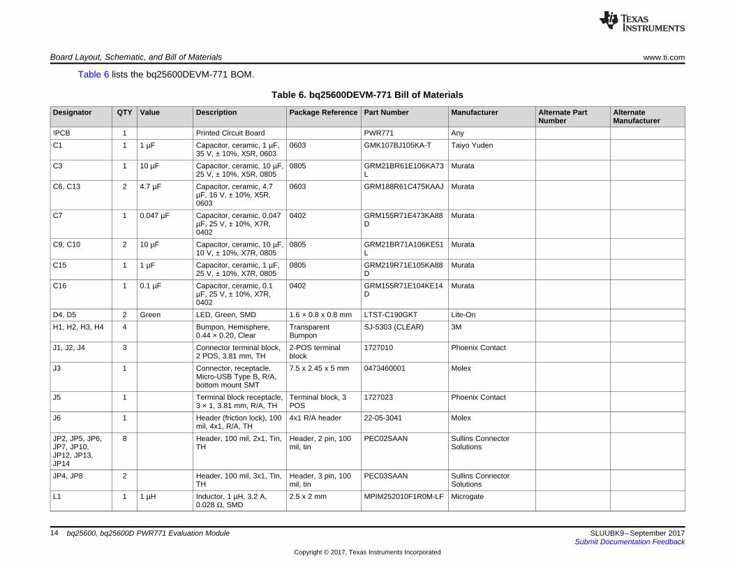
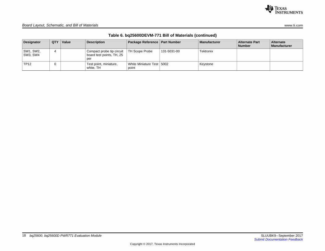
Table 6 lists the bq25600DEVM-771 BOM.
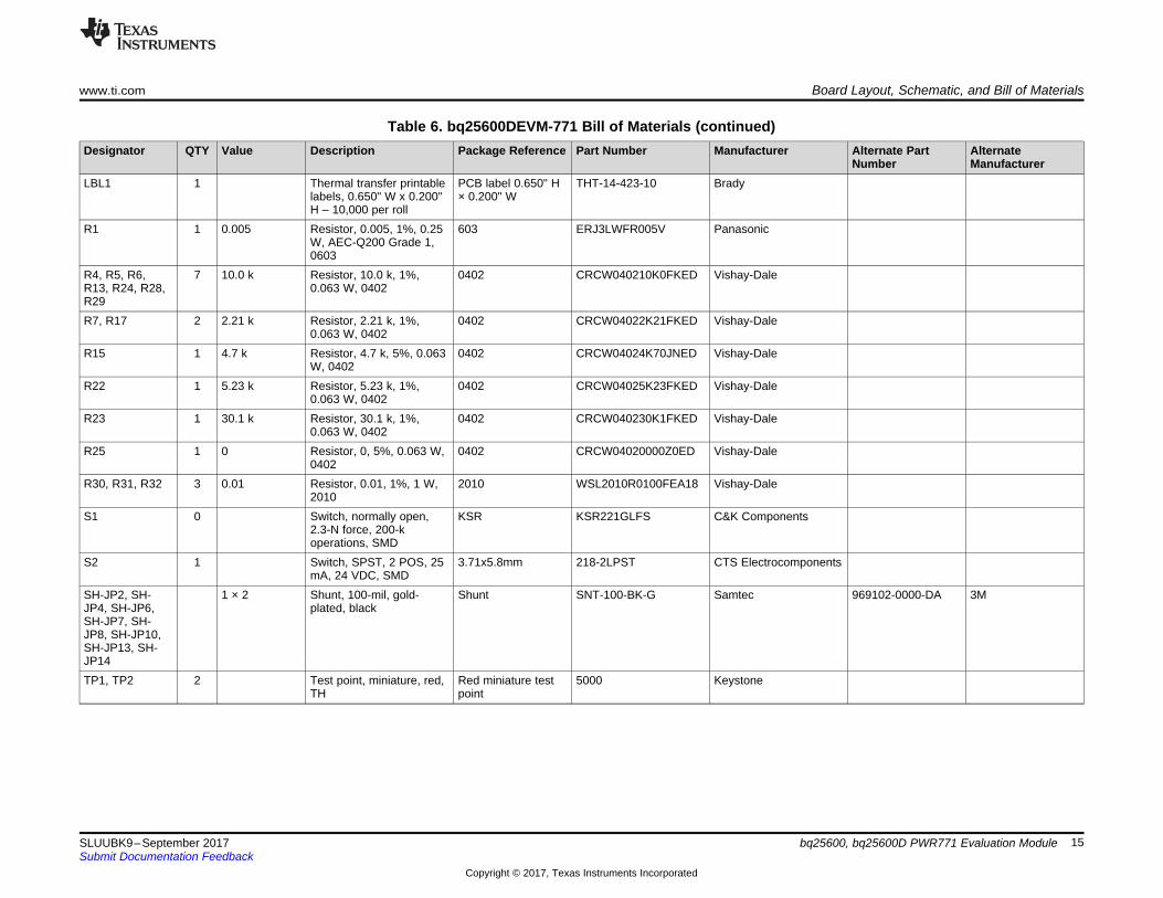
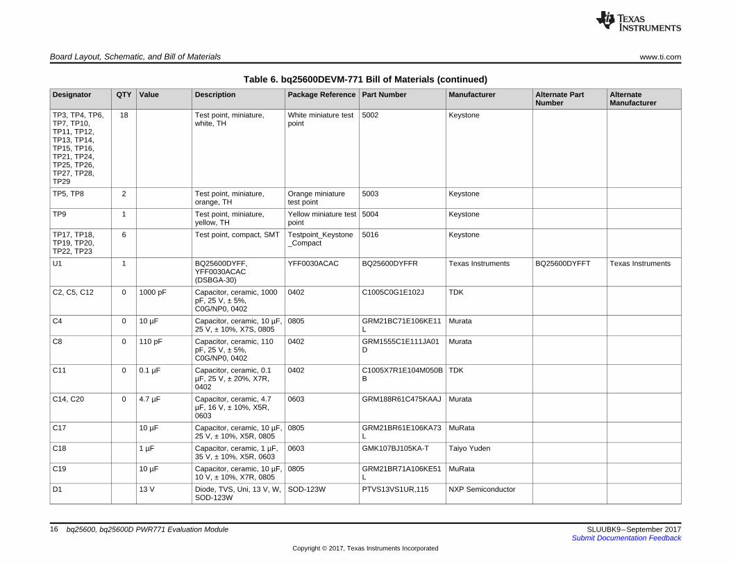
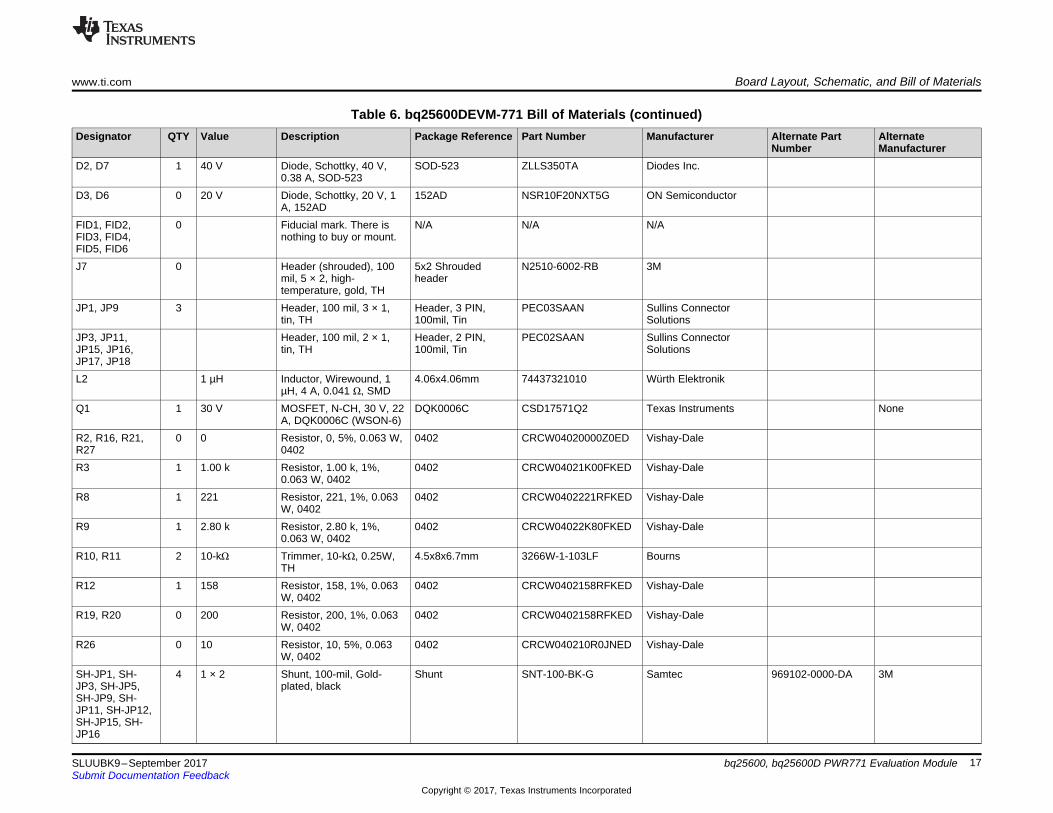
Table 6. bq25600DEVM-771 Bill of Materials
Designator QTY Value Description Package Reference Part Number Manufacturer Alternate PartNumber
AlternateManufacturer
!PCB 1 Printed Circuit Board PWR771 AnyC1 1 1 µF Capacitor, ceramic, 1 µF,
35 V, ± 10%, X5R, 06030603 GMK107BJ105KA-T Taiyo Yuden
C3 1 10 µF Capacitor, ceramic, 10 µF,25 V, ± 10%, X5R, 0805
0805 GRM21BR61E106KA73L
Murata
C6, C13 2 4.7 µF Capacitor, ceramic, 4.7µF, 16 V, ± 10%, X5R,0603
0603 GRM188R61C475KAAJ Murata
C7 1 0.047 µF Capacitor, ceramic, 0.047µF, 25 V, ± 10%, X7R,0402
0402 GRM155R71E473KA88D
Murata
C9, C10 2 10 µF Capacitor, ceramic, 10 µF,10 V, ± 10%, X7R, 0805
0805 GRM21BR71A106KE51L
Murata
C15 1 1 µF Capacitor, ceramic, 1 µF,25 V, ± 10%, X7R, 0805
0805 GRM219R71E105KA88D
Murata
C16 1 0.1 µF Capacitor, ceramic, 0.1µF, 25 V, ± 10%, X7R,0402
0402 GRM155R71E104KE14D
Murata
D4, D5 2 Green LED, Green, SMD 1.6 × 0.8 x 0.8 mm LTST-C190GKT Lite-OnH1, H2, H3, H4 4 Bumpon, Hemisphere,
0.44 × 0.20, ClearTransparentBumpon
SJ-5303 (CLEAR) 3M
J1, J2, J4 3 Connector terminal block,2 POS, 3.81 mm, TH
2-POS terminalblock
1727010 Phoenix Contact
J3 1 Connector, receptacle,Micro-USB Type B, R/A,bottom mount SMT
7.5 x 2.45 x 5 mm 0473460001 Molex
J5 1 Terminal block receptacle,3 × 1, 3.81 mm, R/A, TH
Terminal block, 3POS
1727023 Phoenix Contact
J6 1 Header (friction lock), 100mil, 4x1, R/A, TH
4x1 R/A header 22-05-3041 Molex
JP2, JP5, JP6,JP7, JP10,JP12, JP13,JP14
8 Header, 100 mil, 2x1, Tin,TH
Header, 2 pin, 100mil, tin
PEC02SAAN Sullins ConnectorSolutions
JP4, JP8 2 Header, 100 mil, 3x1, Tin,TH
Header, 3 pin, 100mil, tin
PEC03SAAN Sullins ConnectorSolutions
L1 1 1 µH Inductor, 1 µH, 3.2 A,0.028 Ω, SMD
2.5 x 2 mm MPIM252010F1R0M-LF Microgate
www.ti.com Board Layout, Schematic, and Bill of Materials
15SLUUBK9–September 2017Submit Documentation Feedback
Copyright © 2017, Texas Instruments Incorporated
bq25600, bq25600D PWR771 Evaluation Module
Table 6. bq25600DEVM-771 Bill of Materials (continued)Designator QTY Value Description Package Reference Part Number Manufacturer Alternate Part
NumberAlternateManufacturer
LBL1 1 Thermal transfer printablelabels, 0.650" W x 0.200"H – 10,000 per roll
PCB label 0.650" H× 0.200" W
THT-14-423-10 Brady
R1 1 0.005 Resistor, 0.005, 1%, 0.25W, AEC-Q200 Grade 1,0603
603 ERJ3LWFR005V Panasonic
R4, R5, R6,R13, R24, R28,R29
7 10.0 k Resistor, 10.0 k, 1%,0.063 W, 0402
0402 CRCW040210K0FKED Vishay-Dale
R7, R17 2 2.21 k Resistor, 2.21 k, 1%,0.063 W, 0402
0402 CRCW04022K21FKED Vishay-Dale
R15 1 4.7 k Resistor, 4.7 k, 5%, 0.063W, 0402
0402 CRCW04024K70JNED Vishay-Dale
R22 1 5.23 k Resistor, 5.23 k, 1%,0.063 W, 0402
0402 CRCW04025K23FKED Vishay-Dale
R23 1 30.1 k Resistor, 30.1 k, 1%,0.063 W, 0402
0402 CRCW040230K1FKED Vishay-Dale
R25 1 0 Resistor, 0, 5%, 0.063 W,0402
0402 CRCW04020000Z0ED Vishay-Dale
R30, R31, R32 3 0.01 Resistor, 0.01, 1%, 1 W,2010
2010 WSL2010R0100FEA18 Vishay-Dale
S1 0 Switch, normally open,2.3-N force, 200-koperations, SMD
KSR KSR221GLFS C&K Components
S2 1 Switch, SPST, 2 POS, 25mA, 24 VDC, SMD
3.71x5.8mm 218-2LPST CTS Electrocomponents
SH-JP2, SH-JP4, SH-JP6,SH-JP7, SH-JP8, SH-JP10,SH-JP13, SH-JP14
1 × 2 Shunt, 100-mil, gold-plated, black
Shunt SNT-100-BK-G Samtec 969102-0000-DA 3M
TP1, TP2 2 Test point, miniature, red,TH
Red miniature testpoint
5000 Keystone
Board Layout, Schematic, and Bill of Materials www.ti.com
16 SLUUBK9–September 2017Submit Documentation Feedback
Copyright © 2017, Texas Instruments Incorporated
bq25600, bq25600D PWR771 Evaluation Module
Table 6. bq25600DEVM-771 Bill of Materials (continued)Designator QTY Value Description Package Reference Part Number Manufacturer Alternate Part
NumberAlternateManufacturer
TP3, TP4, TP6,TP7, TP10,TP11, TP12,TP13, TP14,TP15, TP16,TP21, TP24,TP25, TP26,TP27, TP28,TP29
18 Test point, miniature,white, TH
White miniature testpoint
5002 Keystone
TP5, TP8 2 Test point, miniature,orange, TH
Orange miniaturetest point
5003 Keystone
TP9 1 Test point, miniature,yellow, TH
Yellow miniature testpoint
5004 Keystone
TP17, TP18,TP19, TP20,TP22, TP23
6 Test point, compact, SMT Testpoint_Keystone_Compact
5016 Keystone
U1 1 BQ25600DYFF,YFF0030ACAC(DSBGA-30)
YFF0030ACAC BQ25600DYFFR Texas Instruments BQ25600DYFFT Texas Instruments
C2, C5, C12 0 1000 pF Capacitor, ceramic, 1000pF, 25 V, ± 5%,C0G/NP0, 0402
0402 C1005C0G1E102J TDK
C4 0 10 µF Capacitor, ceramic, 10 µF,25 V, ± 10%, X7S, 0805
0805 GRM21BC71E106KE11L
Murata
C8 0 110 pF Capacitor, ceramic, 110pF, 25 V, ± 5%,C0G/NP0, 0402
0402 GRM1555C1E111JA01D
Murata
C11 0 0.1 µF Capacitor, ceramic, 0.1µF, 25 V, ± 20%, X7R,0402
0402 C1005X7R1E104M050BB
TDK
C14, C20 0 4.7 µF Capacitor, ceramic, 4.7µF, 16 V, ± 10%, X5R,0603
0603 GRM188R61C475KAAJ Murata
C17 10 µF Capacitor, ceramic, 10 µF,25 V, ± 10%, X5R, 0805
0805 GRM21BR61E106KA73L
MuRata
C18 1 µF Capacitor, ceramic, 1 µF,35 V, ± 10%, X5R, 0603
0603 GMK107BJ105KA-T Taiyo Yuden
C19 10 µF Capacitor, ceramic, 10 µF,10 V, ± 10%, X7R, 0805
0805 GRM21BR71A106KE51L
MuRata
D1 13 V Diode, TVS, Uni, 13 V, W,SOD-123W
SOD-123W PTVS13VS1UR,115 NXP Semiconductor
www.ti.com Board Layout, Schematic, and Bill of Materials
17SLUUBK9–September 2017Submit Documentation Feedback
Copyright © 2017, Texas Instruments Incorporated
bq25600, bq25600D PWR771 Evaluation Module
Table 6. bq25600DEVM-771 Bill of Materials (continued)Designator QTY Value Description Package Reference Part Number Manufacturer Alternate Part
NumberAlternateManufacturer
D2, D7 1 40 V Diode, Schottky, 40 V,0.38 A, SOD-523
SOD-523 ZLLS350TA Diodes Inc.
D3, D6 0 20 V Diode, Schottky, 20 V, 1A, 152AD
152AD NSR10F20NXT5G ON Semiconductor
FID1, FID2,FID3, FID4,FID5, FID6
0 Fiducial mark. There isnothing to buy or mount.
N/A N/A N/A
J7 0 Header (shrouded), 100mil, 5 × 2, high-temperature, gold, TH
5x2 Shroudedheader
N2510-6002-RB 3M
JP1, JP9 3 Header, 100 mil, 3 × 1,tin, TH
Header, 3 PIN,100mil, Tin
PEC03SAAN Sullins ConnectorSolutions
JP3, JP11,JP15, JP16,JP17, JP18
Header, 100 mil, 2 × 1,tin, TH
Header, 2 PIN,100mil, Tin
PEC02SAAN Sullins ConnectorSolutions
L2 1 µH Inductor, Wirewound, 1µH, 4 A, 0.041 Ω, SMD
4.06x4.06mm 74437321010 Würth Elektronik
Q1 1 30 V MOSFET, N-CH, 30 V, 22A, DQK0006C (WSON-6)
DQK0006C CSD17571Q2 Texas Instruments None
R2, R16, R21,R27
0 0 Resistor, 0, 5%, 0.063 W,0402
0402 CRCW04020000Z0ED Vishay-Dale
R3 1 1.00 k Resistor, 1.00 k, 1%,0.063 W, 0402
0402 CRCW04021K00FKED Vishay-Dale
R8 1 221 Resistor, 221, 1%, 0.063W, 0402
0402 CRCW0402221RFKED Vishay-Dale
R9 1 2.80 k Resistor, 2.80 k, 1%,0.063 W, 0402
0402 CRCW04022K80FKED Vishay-Dale
R10, R11 2 10-kΩ Trimmer, 10-kΩ, 0.25W,TH
4.5x8x6.7mm 3266W-1-103LF Bourns
R12 1 158 Resistor, 158, 1%, 0.063W, 0402
0402 CRCW0402158RFKED Vishay-Dale
R19, R20 0 200 Resistor, 200, 1%, 0.063W, 0402
0402 CRCW0402158RFKED Vishay-Dale
R26 0 10 Resistor, 10, 5%, 0.063W, 0402
0402 CRCW040210R0JNED Vishay-Dale
SH-JP1, SH-JP3, SH-JP5,SH-JP9, SH-JP11, SH-JP12,SH-JP15, SH-JP16
4 1 × 2 Shunt, 100-mil, Gold-plated, black
Shunt SNT-100-BK-G Samtec 969102-0000-DA 3M
Board Layout, Schematic, and Bill of Materials www.ti.com
18 SLUUBK9–September 2017Submit Documentation Feedback
Copyright © 2017, Texas Instruments Incorporated
bq25600, bq25600D PWR771 Evaluation Module
Table 6. bq25600DEVM-771 Bill of Materials (continued)Designator QTY Value Description Package Reference Part Number Manufacturer Alternate Part
NumberAlternateManufacturer
SW1, SW2,SW3, SW4
4 Compact probe tip circuitboard test points, TH, 25per
TH Scope Probe 131-5031-00 Tektronix
TP12 0 Test point, miniature,white, TH
White Miniature Testpoint
5002 Keystone
STANDARD TERMS FOR EVALUATION MODULES1. Delivery: TI delivers TI evaluation boards, kits, or modules, including any accompanying demonstration software, components, and/or
documentation which may be provided together or separately (collectively, an “EVM” or “EVMs”) to the User (“User”) in accordancewith the terms set forth herein. User's acceptance of the EVM is expressly subject to the following terms.1.1 EVMs are intended solely for product or software developers for use in a research and development setting to facilitate feasibility
evaluation, experimentation, or scientific analysis of TI semiconductors products. EVMs have no direct function and are notfinished products. EVMs shall not be directly or indirectly assembled as a part or subassembly in any finished product. Forclarification, any software or software tools provided with the EVM (“Software”) shall not be subject to the terms and conditionsset forth herein but rather shall be subject to the applicable terms that accompany such Software
1.2 EVMs are not intended for consumer or household use. EVMs may not be sold, sublicensed, leased, rented, loaned, assigned,or otherwise distributed for commercial purposes by Users, in whole or in part, or used in any finished product or productionsystem.
2 Limited Warranty and Related Remedies/Disclaimers:2.1 These terms do not apply to Software. The warranty, if any, for Software is covered in the applicable Software License
Agreement.2.2 TI warrants that the TI EVM will conform to TI's published specifications for ninety (90) days after the date TI delivers such EVM
to User. Notwithstanding the foregoing, TI shall not be liable for a nonconforming EVM if (a) the nonconformity was caused byneglect, misuse or mistreatment by an entity other than TI, including improper installation or testing, or for any EVMs that havebeen altered or modified in any way by an entity other than TI, (b) the nonconformity resulted from User's design, specificationsor instructions for such EVMs or improper system design, or (c) User has not paid on time. Testing and other quality controltechniques are used to the extent TI deems necessary. TI does not test all parameters of each EVM.User's claims against TI under this Section 2 are void if User fails to notify TI of any apparent defects in the EVMs within ten (10)business days after delivery, or of any hidden defects with ten (10) business days after the defect has been detected.
2.3 TI's sole liability shall be at its option to repair or replace EVMs that fail to conform to the warranty set forth above, or creditUser's account for such EVM. TI's liability under this warranty shall be limited to EVMs that are returned during the warrantyperiod to the address designated by TI and that are determined by TI not to conform to such warranty. If TI elects to repair orreplace such EVM, TI shall have a reasonable time to repair such EVM or provide replacements. Repaired EVMs shall bewarranted for the remainder of the original warranty period. Replaced EVMs shall be warranted for a new full ninety (90) daywarranty period.
3 Regulatory Notices:3.1 United States
3.1.1 Notice applicable to EVMs not FCC-Approved:FCC NOTICE: This kit is designed to allow product developers to evaluate electronic components, circuitry, or softwareassociated with the kit to determine whether to incorporate such items in a finished product and software developers to writesoftware applications for use with the end product. This kit is not a finished product and when assembled may not be resold orotherwise marketed unless all required FCC equipment authorizations are first obtained. Operation is subject to the conditionthat this product not cause harmful interference to licensed radio stations and that this product accept harmful interference.Unless the assembled kit is designed to operate under part 15, part 18 or part 95 of this chapter, the operator of the kit mustoperate under the authority of an FCC license holder or must secure an experimental authorization under part 5 of this chapter.3.1.2 For EVMs annotated as FCC – FEDERAL COMMUNICATIONS COMMISSION Part 15 Compliant:
CAUTIONThis device complies with part 15 of the FCC Rules. Operation is subject to the following two conditions: (1) This device may notcause harmful interference, and (2) this device must accept any interference received, including interference that may causeundesired operation.Changes or modifications not expressly approved by the party responsible for compliance could void the user's authority tooperate the equipment.
FCC Interference Statement for Class A EVM devicesNOTE: This equipment has been tested and found to comply with the limits for a Class A digital device, pursuant to part 15 ofthe FCC Rules. These limits are designed to provide reasonable protection against harmful interference when the equipment isoperated in a commercial environment. This equipment generates, uses, and can radiate radio frequency energy and, if notinstalled and used in accordance with the instruction manual, may cause harmful interference to radio communications.Operation of this equipment in a residential area is likely to cause harmful interference in which case the user will be required tocorrect the interference at his own expense.
FCC Interference Statement for Class B EVM devicesNOTE: This equipment has been tested and found to comply with the limits for a Class B digital device, pursuant to part 15 ofthe FCC Rules. These limits are designed to provide reasonable protection against harmful interference in a residentialinstallation. This equipment generates, uses and can radiate radio frequency energy and, if not installed and used in accordancewith the instructions, may cause harmful interference to radio communications. However, there is no guarantee that interferencewill not occur in a particular installation. If this equipment does cause harmful interference to radio or television reception, whichcan be determined by turning the equipment off and on, the user is encouraged to try to correct the interference by one or moreof the following measures:
• Reorient or relocate the receiving antenna.• Increase the separation between the equipment and receiver.• Connect the equipment into an outlet on a circuit different from that to which the receiver is connected.• Consult the dealer or an experienced radio/TV technician for help.
3.2 Canada3.2.1 For EVMs issued with an Industry Canada Certificate of Conformance to RSS-210 or RSS-247
Concerning EVMs Including Radio Transmitters:This device complies with Industry Canada license-exempt RSSs. Operation is subject to the following two conditions:(1) this device may not cause interference, and (2) this device must accept any interference, including interference that maycause undesired operation of the device.
Concernant les EVMs avec appareils radio:Le présent appareil est conforme aux CNR d'Industrie Canada applicables aux appareils radio exempts de licence. L'exploitationest autorisée aux deux conditions suivantes: (1) l'appareil ne doit pas produire de brouillage, et (2) l'utilisateur de l'appareil doitaccepter tout brouillage radioélectrique subi, même si le brouillage est susceptible d'en compromettre le fonctionnement.
Concerning EVMs Including Detachable Antennas:Under Industry Canada regulations, this radio transmitter may only operate using an antenna of a type and maximum (or lesser)gain approved for the transmitter by Industry Canada. To reduce potential radio interference to other users, the antenna typeand its gain should be so chosen that the equivalent isotropically radiated power (e.i.r.p.) is not more than that necessary forsuccessful communication. This radio transmitter has been approved by Industry Canada to operate with the antenna typeslisted in the user guide with the maximum permissible gain and required antenna impedance for each antenna type indicated.Antenna types not included in this list, having a gain greater than the maximum gain indicated for that type, are strictly prohibitedfor use with this device.
Concernant les EVMs avec antennes détachablesConformément à la réglementation d'Industrie Canada, le présent émetteur radio peut fonctionner avec une antenne d'un type etd'un gain maximal (ou inférieur) approuvé pour l'émetteur par Industrie Canada. Dans le but de réduire les risques de brouillageradioélectrique à l'intention des autres utilisateurs, il faut choisir le type d'antenne et son gain de sorte que la puissance isotroperayonnée équivalente (p.i.r.e.) ne dépasse pas l'intensité nécessaire à l'établissement d'une communication satisfaisante. Leprésent émetteur radio a été approuvé par Industrie Canada pour fonctionner avec les types d'antenne énumérés dans lemanuel d’usage et ayant un gain admissible maximal et l'impédance requise pour chaque type d'antenne. Les types d'antennenon inclus dans cette liste, ou dont le gain est supérieur au gain maximal indiqué, sont strictement interdits pour l'exploitation del'émetteur
3.3 Japan3.3.1 Notice for EVMs delivered in Japan: Please see http://www.tij.co.jp/lsds/ti_ja/general/eStore/notice_01.page 日本国内に
輸入される評価用キット、ボードについては、次のところをご覧ください。http://www.tij.co.jp/lsds/ti_ja/general/eStore/notice_01.page
3.3.2 Notice for Users of EVMs Considered “Radio Frequency Products” in Japan: EVMs entering Japan may not be certifiedby TI as conforming to Technical Regulations of Radio Law of Japan.
If User uses EVMs in Japan, not certified to Technical Regulations of Radio Law of Japan, User is required to follow theinstructions set forth by Radio Law of Japan, which includes, but is not limited to, the instructions below with respect to EVMs(which for the avoidance of doubt are stated strictly for convenience and should be verified by User):1. Use EVMs in a shielded room or any other test facility as defined in the notification #173 issued by Ministry of Internal
Affairs and Communications on March 28, 2006, based on Sub-section 1.1 of Article 6 of the Ministry’s Rule forEnforcement of Radio Law of Japan,
2. Use EVMs only after User obtains the license of Test Radio Station as provided in Radio Law of Japan with respect toEVMs, or
3. Use of EVMs only after User obtains the Technical Regulations Conformity Certification as provided in Radio Law of Japanwith respect to EVMs. Also, do not transfer EVMs, unless User gives the same notice above to the transferee. Please notethat if User does not follow the instructions above, User will be subject to penalties of Radio Law of Japan.
【無線電波を送信する製品の開発キットをお使いになる際の注意事項】 開発キットの中には技術基準適合証明を受けていないものがあります。 技術適合証明を受けていないもののご使用に際しては、電波法遵守のため、以下のいずれかの措置を取っていただく必要がありますのでご注意ください。1. 電波法施行規則第6条第1項第1号に基づく平成18年3月28日総務省告示第173号で定められた電波暗室等の試験設備でご使用
いただく。2. 実験局の免許を取得後ご使用いただく。3. 技術基準適合証明を取得後ご使用いただく。
なお、本製品は、上記の「ご使用にあたっての注意」を譲渡先、移転先に通知しない限り、譲渡、移転できないものとします。上記を遵守頂けない場合は、電波法の罰則が適用される可能性があることをご留意ください。 日本テキサス・イ
ンスツルメンツ株式会社東京都新宿区西新宿6丁目24番1号西新宿三井ビル
3.3.3 Notice for EVMs for Power Line Communication: Please see http://www.tij.co.jp/lsds/ti_ja/general/eStore/notice_02.page電力線搬送波通信についての開発キットをお使いになる際の注意事項については、次のところをご覧ください。http://www.tij.co.jp/lsds/ti_ja/general/eStore/notice_02.page
3.4 European Union3.4.1 For EVMs subject to EU Directive 2014/30/EU (Electromagnetic Compatibility Directive):
This is a class A product intended for use in environments other than domestic environments that are connected to alow-voltage power-supply network that supplies buildings used for domestic purposes. In a domestic environment thisproduct may cause radio interference in which case the user may be required to take adequate measures.
4 EVM Use Restrictions and Warnings:4.1 EVMS ARE NOT FOR USE IN FUNCTIONAL SAFETY AND/OR SAFETY CRITICAL EVALUATIONS, INCLUDING BUT NOT
LIMITED TO EVALUATIONS OF LIFE SUPPORT APPLICATIONS.4.2 User must read and apply the user guide and other available documentation provided by TI regarding the EVM prior to handling
or using the EVM, including without limitation any warning or restriction notices. The notices contain important safety informationrelated to, for example, temperatures and voltages.
4.3 Safety-Related Warnings and Restrictions:4.3.1 User shall operate the EVM within TI’s recommended specifications and environmental considerations stated in the user
guide, other available documentation provided by TI, and any other applicable requirements and employ reasonable andcustomary safeguards. Exceeding the specified performance ratings and specifications (including but not limited to inputand output voltage, current, power, and environmental ranges) for the EVM may cause personal injury or death, orproperty damage. If there are questions concerning performance ratings and specifications, User should contact a TIfield representative prior to connecting interface electronics including input power and intended loads. Any loads appliedoutside of the specified output range may also result in unintended and/or inaccurate operation and/or possiblepermanent damage to the EVM and/or interface electronics. Please consult the EVM user guide prior to connecting anyload to the EVM output. If there is uncertainty as to the load specification, please contact a TI field representative.During normal operation, even with the inputs and outputs kept within the specified allowable ranges, some circuitcomponents may have elevated case temperatures. These components include but are not limited to linear regulators,switching transistors, pass transistors, current sense resistors, and heat sinks, which can be identified using theinformation in the associated documentation. When working with the EVM, please be aware that the EVM may becomevery warm.
4.3.2 EVMs are intended solely for use by technically qualified, professional electronics experts who are familiar with thedangers and application risks associated with handling electrical mechanical components, systems, and subsystems.User assumes all responsibility and liability for proper and safe handling and use of the EVM by User or its employees,affiliates, contractors or designees. User assumes all responsibility and liability to ensure that any interfaces (electronicand/or mechanical) between the EVM and any human body are designed with suitable isolation and means to safelylimit accessible leakage currents to minimize the risk of electrical shock hazard. User assumes all responsibility andliability for any improper or unsafe handling or use of the EVM by User or its employees, affiliates, contractors ordesignees.
4.4 User assumes all responsibility and liability to determine whether the EVM is subject to any applicable international, federal,state, or local laws and regulations related to User’s handling and use of the EVM and, if applicable, User assumes allresponsibility and liability for compliance in all respects with such laws and regulations. User assumes all responsibility andliability for proper disposal and recycling of the EVM consistent with all applicable international, federal, state, and localrequirements.
5. Accuracy of Information: To the extent TI provides information on the availability and function of EVMs, TI attempts to be as accurateas possible. However, TI does not warrant the accuracy of EVM descriptions, EVM availability or other information on its websites asaccurate, complete, reliable, current, or error-free.
6. Disclaimers:6.1 EXCEPT AS SET FORTH ABOVE, EVMS AND ANY MATERIALS PROVIDED WITH THE EVM (INCLUDING, BUT NOT
LIMITED TO, REFERENCE DESIGNS AND THE DESIGN OF THE EVM ITSELF) ARE PROVIDED "AS IS" AND "WITH ALLFAULTS." TI DISCLAIMS ALL OTHER WARRANTIES, EXPRESS OR IMPLIED, REGARDING SUCH ITEMS, INCLUDING BUTNOT LIMITED TO ANY EPIDEMIC FAILURE WARRANTY OR IMPLIED WARRANTIES OF MERCHANTABILITY OR FITNESSFOR A PARTICULAR PURPOSE OR NON-INFRINGEMENT OF ANY THIRD PARTY PATENTS, COPYRIGHTS, TRADESECRETS OR OTHER INTELLECTUAL PROPERTY RIGHTS.
6.2 EXCEPT FOR THE LIMITED RIGHT TO USE THE EVM SET FORTH HEREIN, NOTHING IN THESE TERMS SHALL BECONSTRUED AS GRANTING OR CONFERRING ANY RIGHTS BY LICENSE, PATENT, OR ANY OTHER INDUSTRIAL ORINTELLECTUAL PROPERTY RIGHT OF TI, ITS SUPPLIERS/LICENSORS OR ANY OTHER THIRD PARTY, TO USE THEEVM IN ANY FINISHED END-USER OR READY-TO-USE FINAL PRODUCT, OR FOR ANY INVENTION, DISCOVERY ORIMPROVEMENT, REGARDLESS OF WHEN MADE, CONCEIVED OR ACQUIRED.
7. USER'S INDEMNITY OBLIGATIONS AND REPRESENTATIONS. USER WILL DEFEND, INDEMNIFY AND HOLD TI, ITSLICENSORS AND THEIR REPRESENTATIVES HARMLESS FROM AND AGAINST ANY AND ALL CLAIMS, DAMAGES, LOSSES,EXPENSES, COSTS AND LIABILITIES (COLLECTIVELY, "CLAIMS") ARISING OUT OF OR IN CONNECTION WITH ANYHANDLING OR USE OF THE EVM THAT IS NOT IN ACCORDANCE WITH THESE TERMS. THIS OBLIGATION SHALL APPLYWHETHER CLAIMS ARISE UNDER STATUTE, REGULATION, OR THE LAW OF TORT, CONTRACT OR ANY OTHER LEGALTHEORY, AND EVEN IF THE EVM FAILS TO PERFORM AS DESCRIBED OR EXPECTED.
8. Limitations on Damages and Liability:8.1 General Limitations. IN NO EVENT SHALL TI BE LIABLE FOR ANY SPECIAL, COLLATERAL, INDIRECT, PUNITIVE,
INCIDENTAL, CONSEQUENTIAL, OR EXEMPLARY DAMAGES IN CONNECTION WITH OR ARISING OUT OF THESETERMS OR THE USE OF THE EVMS , REGARDLESS OF WHETHER TI HAS BEEN ADVISED OF THE POSSIBILITY OFSUCH DAMAGES. EXCLUDED DAMAGES INCLUDE, BUT ARE NOT LIMITED TO, COST OF REMOVAL ORREINSTALLATION, ANCILLARY COSTS TO THE PROCUREMENT OF SUBSTITUTE GOODS OR SERVICES, RETESTING,OUTSIDE COMPUTER TIME, LABOR COSTS, LOSS OF GOODWILL, LOSS OF PROFITS, LOSS OF SAVINGS, LOSS OFUSE, LOSS OF DATA, OR BUSINESS INTERRUPTION. NO CLAIM, SUIT OR ACTION SHALL BE BROUGHT AGAINST TIMORE THAN TWELVE (12) MONTHS AFTER THE EVENT THAT GAVE RISE TO THE CAUSE OF ACTION HASOCCURRED.
8.2 Specific Limitations. IN NO EVENT SHALL TI'S AGGREGATE LIABILITY FROM ANY USE OF AN EVM PROVIDEDHEREUNDER, INCLUDING FROM ANY WARRANTY, INDEMITY OR OTHER OBLIGATION ARISING OUT OF OR INCONNECTION WITH THESE TERMS, , EXCEED THE TOTAL AMOUNT PAID TO TI BY USER FOR THE PARTICULAREVM(S) AT ISSUE DURING THE PRIOR TWELVE (12) MONTHS WITH RESPECT TO WHICH LOSSES OR DAMAGES ARECLAIMED. THE EXISTENCE OF MORE THAN ONE CLAIM SHALL NOT ENLARGE OR EXTEND THIS LIMIT.
9. Return Policy. Except as otherwise provided, TI does not offer any refunds, returns, or exchanges. Furthermore, no return of EVM(s)will be accepted if the package has been opened and no return of the EVM(s) will be accepted if they are damaged or otherwise not ina resalable condition. If User feels it has been incorrectly charged for the EVM(s) it ordered or that delivery violates the applicableorder, User should contact TI. All refunds will be made in full within thirty (30) working days from the return of the components(s),excluding any postage or packaging costs.
10. Governing Law: These terms and conditions shall be governed by and interpreted in accordance with the laws of the State of Texas,without reference to conflict-of-laws principles. User agrees that non-exclusive jurisdiction for any dispute arising out of or relating tothese terms and conditions lies within courts located in the State of Texas and consents to venue in Dallas County, Texas.Notwithstanding the foregoing, any judgment may be enforced in any United States or foreign court, and TI may seek injunctive reliefin any United States or foreign court.
Mailing Address: Texas Instruments, Post Office Box 655303, Dallas, Texas 75265Copyright © 2017, Texas Instruments Incorporated
IMPORTANT NOTICE FOR TI DESIGN INFORMATION AND RESOURCES
Texas Instruments Incorporated (‘TI”) technical, application or other design advice, services or information, including, but not limited to,reference designs and materials relating to evaluation modules, (collectively, “TI Resources”) are intended to assist designers who aredeveloping applications that incorporate TI products; by downloading, accessing or using any particular TI Resource in any way, you(individually or, if you are acting on behalf of a company, your company) agree to use it solely for this purpose and subject to the terms ofthis Notice.TI’s provision of TI Resources does not expand or otherwise alter TI’s applicable published warranties or warranty disclaimers for TIproducts, and no additional obligations or liabilities arise from TI providing such TI Resources. TI reserves the right to make corrections,enhancements, improvements and other changes to its TI Resources.You understand and agree that you remain responsible for using your independent analysis, evaluation and judgment in designing yourapplications and that you have full and exclusive responsibility to assure the safety of your applications and compliance of your applications(and of all TI products used in or for your applications) with all applicable regulations, laws and other applicable requirements. Yourepresent that, with respect to your applications, you have all the necessary expertise to create and implement safeguards that (1)anticipate dangerous consequences of failures, (2) monitor failures and their consequences, and (3) lessen the likelihood of failures thatmight cause harm and take appropriate actions. You agree that prior to using or distributing any applications that include TI products, youwill thoroughly test such applications and the functionality of such TI products as used in such applications. TI has not conducted anytesting other than that specifically described in the published documentation for a particular TI Resource.You are authorized to use, copy and modify any individual TI Resource only in connection with the development of applications that includethe TI product(s) identified in such TI Resource. NO OTHER LICENSE, EXPRESS OR IMPLIED, BY ESTOPPEL OR OTHERWISE TOANY OTHER TI INTELLECTUAL PROPERTY RIGHT, AND NO LICENSE TO ANY TECHNOLOGY OR INTELLECTUAL PROPERTYRIGHT OF TI OR ANY THIRD PARTY IS GRANTED HEREIN, including but not limited to any patent right, copyright, mask work right, orother intellectual property right relating to any combination, machine, or process in which TI products or services are used. Informationregarding or referencing third-party products or services does not constitute a license to use such products or services, or a warranty orendorsement thereof. Use of TI Resources may require a license from a third party under the patents or other intellectual property of thethird party, or a license from TI under the patents or other intellectual property of TI.TI RESOURCES ARE PROVIDED “AS IS” AND WITH ALL FAULTS. TI DISCLAIMS ALL OTHER WARRANTIES ORREPRESENTATIONS, EXPRESS OR IMPLIED, REGARDING TI RESOURCES OR USE THEREOF, INCLUDING BUT NOT LIMITED TOACCURACY OR COMPLETENESS, TITLE, ANY EPIDEMIC FAILURE WARRANTY AND ANY IMPLIED WARRANTIES OFMERCHANTABILITY, FITNESS FOR A PARTICULAR PURPOSE, AND NON-INFRINGEMENT OF ANY THIRD PARTY INTELLECTUALPROPERTY RIGHTS.TI SHALL NOT BE LIABLE FOR AND SHALL NOT DEFEND OR INDEMNIFY YOU AGAINST ANY CLAIM, INCLUDING BUT NOTLIMITED TO ANY INFRINGEMENT CLAIM THAT RELATES TO OR IS BASED ON ANY COMBINATION OF PRODUCTS EVEN IFDESCRIBED IN TI RESOURCES OR OTHERWISE. IN NO EVENT SHALL TI BE LIABLE FOR ANY ACTUAL, DIRECT, SPECIAL,COLLATERAL, INDIRECT, PUNITIVE, INCIDENTAL, CONSEQUENTIAL OR EXEMPLARY DAMAGES IN CONNECTION WITH ORARISING OUT OF TI RESOURCES OR USE THEREOF, AND REGARDLESS OF WHETHER TI HAS BEEN ADVISED OF THEPOSSIBILITY OF SUCH DAMAGES.You agree to fully indemnify TI and its representatives against any damages, costs, losses, and/or liabilities arising out of your non-compliance with the terms and provisions of this Notice.This Notice applies to TI Resources. Additional terms apply to the use and purchase of certain types of materials, TI products and services.These include; without limitation, TI’s standard terms for semiconductor products http://www.ti.com/sc/docs/stdterms.htm), evaluationmodules, and samples (http://www.ti.com/sc/docs/sampterms.htm).
Mailing Address: Texas Instruments, Post Office Box 655303, Dallas, Texas 75265Copyright © 2017, Texas Instruments Incorporated