Embed Size (px)
Citation preview
INVBUS
GND
HOST
bq25100B
OUT
1ÛF 1ÛF
SYSTEM
D+
D-
USB Port or Adapter
ISET
PRETERM
TEMPPACK+
PACK-
TS
VSS
CE
1.35k
6k
Copyright © 2016, Texas Instruments Incorporated
Product
Folder
Sample &Buy
Technical
Documents
Tools &
Software
Support &Community
An IMPORTANT NOTICE at the end of this data sheet addresses availability, warranty, changes, use in safety-critical applications,intellectual property matters and other important disclaimers. PRODUCTION DATA.
bq25100BSLUSCG5A –MAY 2016–REVISED JULY 2016
bq25100B 250-mA Single Cell Li-Ion Battery Chargers, 1-mA Termination,75-nA Battery Leakage
1
1 Features1• Charging
– 1% Charge Voltage Accuracy– 10% Charge Current Accuracy– Supports Applications for Very Low Charge
Currents - 10 mA to 250 mA– Supports Minimum 1-mA Charge Termination
Current– Ultra Low Battery Output Leakage Current -
Maximum 75 nA– Adjustable Termination and Precharge
Threshold– High voltage Chemistry Support: 4.30 V
• Protection– 30-V Input Rating; with 6.5-V Input
Overvoltage Protection– Input Voltage Dynamic Power Management– 125°C Thermal Regulation; 150°C Thermal
Shutdown Protection– OUT Short-Circuit Protection and ISET Short
Detection– Fixed 10 Hour Safety Timer
• System– Automatic Termination and Timer Disable
Mode (TTDM) for Absent Battery Pack– Available in Small 1.60 mm × 0.90 mm
DSBGA Package
2 Applications• Fitness Accessories• Smart Watches• Bluetooth® Headsets• Low-Power Handheld Devices
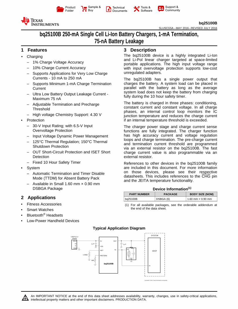
3 DescriptionThe bq25100B device is a highly integrated Li-Ionand Li-Pol linear charger targeted at space-limitedportable applications. The high input voltage rangewith input overvoltage protection supports low-costunregulated adapters.
The bq25100B has a single power output thatcharges the battery. A system load can be placed inparallel with the battery as long as the averagesystem load does not keep the battery from chargingfully during the 10 hour safety timer.
The battery is charged in three phases: conditioning,constant current and constant voltage. In all chargephases, an internal control loop monitors the ICjunction temperature and reduces the charge currentif an internal temperature threshold is exceeded.
The charger power stage and charge current sensefunctions are fully integrated. The charger functionhas high accuracy current and voltage regulationloops and charge termination. The pre-charge currentand termination current threshold are programmedvia an external resistor on the bq25100B. The fastcharge current value is also programmable via anexternal resistor.
References to other devices in the bq25100B familyare included in this document. For more informationon those devices, please see their respectivedatasheets. This includes references to the CHG pinand the JEITA temperature functionality.
Device Information(1)
PART NUMBER PACKAGE BODY SIZE (NOM)
bq25100B DSBGA (6) 1.60 mm × 0.90 mm
(1) For all available packages, see the orderable addendum atthe end of the data sheet.
Typical Application Diagram
2
bq25100BSLUSCG5A –MAY 2016–REVISED JULY 2016 www.ti.com
Product Folder Links: bq25100B
Submit Documentation Feedback Copyright © 2016, Texas Instruments Incorporated
Table of Contents1 Features .................................................................. 12 Applications ........................................................... 13 Description ............................................................. 14 Revision History..................................................... 25 Device Comparison Table ..................................... 36 Pin Configuration and Functions ......................... 37 Specifications......................................................... 4
7.1 Absolute Maximum Ratings ..................................... 47.2 ESD Ratings.............................................................. 47.3 Recommended Operating Conditions...................... 47.4 Thermal Information .................................................. 57.5 Electrical Characteristics.......................................... 57.6 Typical Characteristics .............................................. 9
8 Detailed Description ............................................ 128.1 Overview ................................................................. 128.2 Functional Block Diagram ....................................... 148.3 Feature Description................................................. 158.4 Device Functional Modes........................................ 18
9 Application and Implementation ........................ 229.1 Application Information............................................ 229.2 Typical Application .................................................. 22
10 Power Supply Recommendations ..................... 2410.1 Leakage Current Effects on Battery Capacity....... 24
11 Layout................................................................... 2511.1 Layout Guidelines ................................................. 2511.2 Layout Example .................................................... 2511.3 Thermal Considerations ........................................ 26
12 Device and Documentation Support ................. 2712.1 Device Support .................................................... 2712.2 Related Links ........................................................ 2712.3 Receiving Notification of Documentation Updates 2712.4 Community Resources.......................................... 2712.5 Trademarks ........................................................... 2712.6 Electrostatic Discharge Caution............................ 2712.7 Glossary ................................................................ 27
13 Mechanical, Packaging, and OrderableInformation ........................................................... 28
4 Revision History
Changes from Original (May 2016) to Revision A Page
• Changed IOUT(SC) values From: 9, 11, 13 To: 10, 12, 14 in the Electrical Characteristics table ............................................. 5• Changed IPRE-TERM values From: 23, 25, 27 To: 24.25, 26.25, 28.25 in the Electrical Characteristics table .......................... 6• Changed the INTC-10k values From: 48.5, 50.5, 52.5 To: 50.5, 52.5, 54.5 in the Electrical Characteristics table ................... 7• Changed the INTC-DIS-10k values From: 27, 30, 33 To: 28, 31, 34 in the Electrical Characteristics table ................................ 7• Changed the VTS-0°C values From: 1230, 1255, 1280 To: 1225, 1250, 1275 in the Electrical Characteristics table ............. 7• Changed the VTS-45°C values From: 253, 268, 283 To: 255, 267, 279 in the Electrical Characteristics table ........................ 7• Changed the VTS-EN-10k values From: 84, 92, 100 To: 83, 91, 99 in the Electrical Characteristics table ............................... 8
OUT IN
TS ISET
PRE-
TERMVSS
A
B
C
1 2
3
bq25100Bwww.ti.com SLUSCG5A –MAY 2016–REVISED JULY 2016
Product Folder Links: bq25100B
Submit Documentation FeedbackCopyright © 2016, Texas Instruments Incorporated
(1) The bq25100B is part of the bq25100 family of devices. Please see Device Support for viewing other devices.(2) Product preview. Contact the local TI representative for device details.
5 Device Comparison Table
PART NUMBER VO(REG) VOVP PreTerm /CHG TSbq25100 4.20 V 6.5 V PreTerm TS (JEITA)bq25101 4.20 V 6.5 V CHG TS (JEITA)
bq25100A 4.30 V 6.5 V PreTerm TSbq25100B (1) 4.284 V 6.5 V PreTerm TSbq25100H 4.35 V 6.5 V PreTerm TS (JEITA)bq25101H 4.35 V 6.5 V CHG TS (JEITA)
bq25100L (2) 4.06 V 6.5 V PreTerm TS
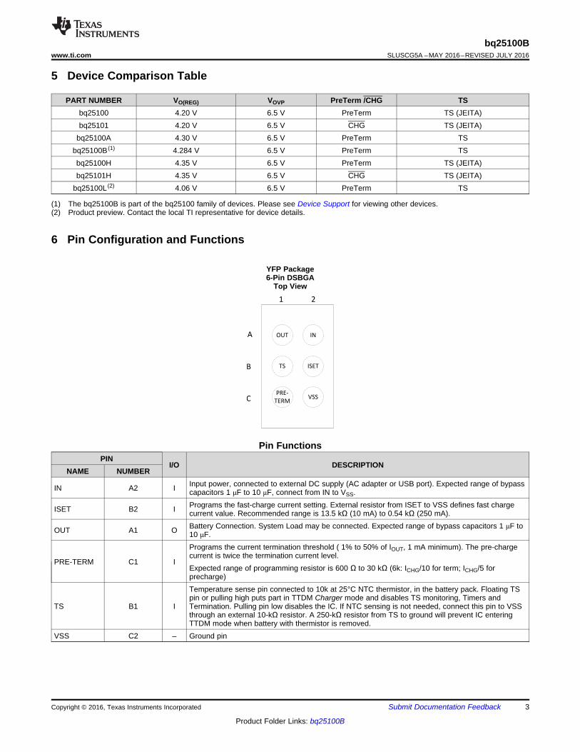
6 Pin Configuration and Functions
YFP Package6-Pin DSBGA
Top View
Pin FunctionsPIN
I/O DESCRIPTIONNAME NUMBER
IN A2 I Input power, connected to external DC supply (AC adapter or USB port). Expected range of bypasscapacitors 1 μF to 10 μF, connect from IN to VSS.
ISET B2 I Programs the fast-charge current setting. External resistor from ISET to VSS defines fast chargecurrent value. Recommended range is 13.5 kΩ (10 mA) to 0.54 kΩ (250 mA).
OUT A1 O Battery Connection. System Load may be connected. Expected range of bypass capacitors 1 μF to10 μF.
PRE-TERM C1 I
Programs the current termination threshold ( 1% to 50% of IOUT, 1 mA minimum). The pre-chargecurrent is twice the termination current level.Expected range of programming resistor is 600 Ω to 30 kΩ (6k: ICHG/10 for term; ICHG/5 forprecharge)
TS B1 I
Temperature sense pin connected to 10k at 25°C NTC thermistor, in the battery pack. Floating TSpin or pulling high puts part in TTDM Charger mode and disables TS monitoring, Timers andTermination. Pulling pin low disables the IC. If NTC sensing is not needed, connect this pin to VSSthrough an external 10-kΩ resistor. A 250-kΩ resistor from TS to ground will prevent IC enteringTTDM mode when battery with thermistor is removed.
VSS C2 – Ground pin
4
bq25100BSLUSCG5A –MAY 2016–REVISED JULY 2016 www.ti.com
Product Folder Links: bq25100B
Submit Documentation Feedback Copyright © 2016, Texas Instruments Incorporated
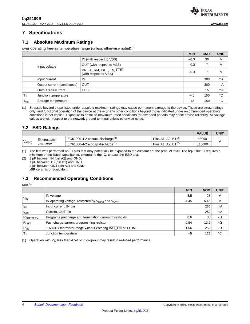
(1) Stresses beyond those listed under absolute maximum ratings may cause permanent damage to the device. These are stress ratingsonly, and functional operation of the device at these or any other conditions beyond those indicated under recommended operatingconditions is not implied. Exposure to absolute-maximum-rated conditions for extended periods may affect device reliability. All voltagevalues are with respect to the network ground terminal unless otherwise noted.
7 Specifications
7.1 Absolute Maximum Ratingsover operating free-air temperature range (unless otherwise noted) (1)
MIN MAX UNIT
Input voltage
IN (with respect to VSS) –0.3 30 VOUT (with respect to VSS) –0.3 7 VPRE-TERM, ISET, TS, CHG(with respect to VSS) –0.3 7 V
Input current IN 300 mAOutput current (continuous) OUT 300 mAOutput sink current CHG 15 mA
TJ Junction temperature –40 150 °CTstg Storage temperature –65 150 °C
(1) The test was performed on IC pins that may potentially be exposed to the customer at the product level. The bq2510x IC requires aminimum of the listed capacitance, external to the IC, to pass the ESD test.
(2) 1 µF between IN (pin A2) and GND,1 µF between TS (pin B1) and GND,2 µF between OUT (pin A1) and GND,x5R ceramic or equivalent
7.2 ESD RatingsVALUE UNIT
V(ESD)Electrostaticdischarge
IEC61000-4-2 contact discharge (1) Pins A1, A2, B1 (2) ±8000V
IEC61000-4-2 air-gap discharge (1) Pins A1, A2, B1 (2) ±15000
(1) Operation with VIN less than 4.5V or in drop-out may result in reduced performance.
7.3 Recommended Operating Conditionssee (1)
MIN NOM UNIT
VININ voltage 3.5 28 VIN operating voltage, restricted by VDPM and VOVP 4.45 6.45 V
IIN Input current, IN pin 250 mAIOUT Current, OUT pin 250 mARPRE-TERM Programs precharge and termination current thresholds 0.6 30 kΩRISET Fast-charge current programming resistor 0.54 13.5 kΩRTS 10k NTC thermistor range without entering BAT_EN or TTDM 1.66 258 kΩTJ Junction temperature –5 125 °C
5
bq25100Bwww.ti.com SLUSCG5A –MAY 2016–REVISED JULY 2016
Product Folder Links: bq25100B
Submit Documentation FeedbackCopyright © 2016, Texas Instruments Incorporated
(1) For more information about traditional and new thermal metrics, see the Semiconductor and IC Package Thermal Metrics applicationreport, SPRA953.
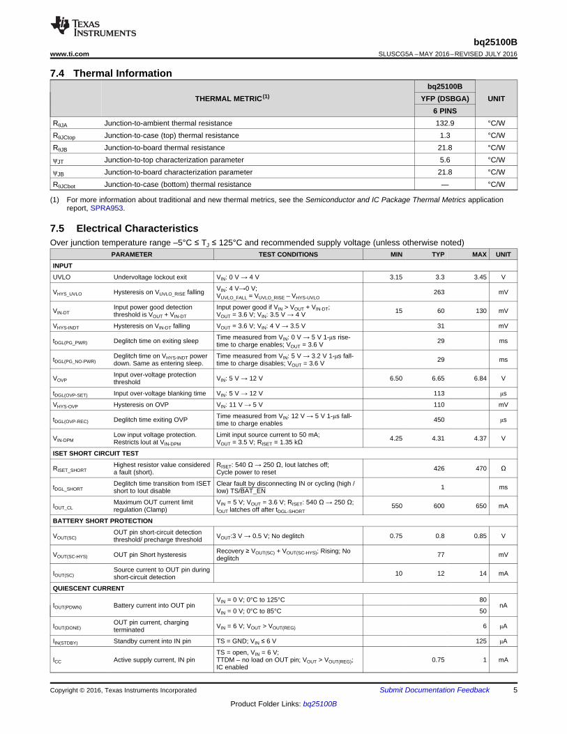
7.4 Thermal Information
THERMAL METRIC (1)bq25100B
UNITYFP (DSBGA)6 PINS
RθJA Junction-to-ambient thermal resistance 132.9 °C/WRθJCtop Junction-to-case (top) thermal resistance 1.3 °C/WRθJB Junction-to-board thermal resistance 21.8 °C/WψJT Junction-to-top characterization parameter 5.6 °C/WψJB Junction-to-board characterization parameter 21.8 °C/WRθJCbot Junction-to-case (bottom) thermal resistance — °C/W
7.5 Electrical CharacteristicsOver junction temperature range –5°C ≤ TJ ≤ 125°C and recommended supply voltage (unless otherwise noted)
PARAMETER TEST CONDITIONS MIN TYP MAX UNIT
INPUT
UVLO Undervoltage lockout exit VIN: 0 V → 4 V 3.15 3.3 3.45 V
VHYS_UVLO Hysteresis on VUVLO_RISE falling VIN: 4 V→0 V;VUVLO_FALL = VUVLO_RISE – VHYS-UVLO
263 mV
VIN-DTInput power good detectionthreshold is VOUT + VIN-DT
Input power good if VIN > VOUT + VIN-DT;VOUT = 3.6 V; VIN: 3.5 V → 4 V 15 60 130 mV
VHYS-INDT Hysteresis on VIN-DT falling VOUT = 3.6 V; VIN: 4 V → 3.5 V 31 mV
tDGL(PG_PWR) Deglitch time on exiting sleep Time measured from VIN: 0 V → 5 V 1-μs rise-time to charge enables; VOUT = 3.6 V 29 ms
tDGL(PG_NO-PWR)Deglitch time on VHYS-INDT powerdown. Same as entering sleep.
Time measured from VIN: 5 V → 3.2 V 1-μs fall-time to charge disables; VOUT = 3.6 V 29 ms
VOVPInput over-voltage protectionthreshold VIN: 5 V → 12 V 6.50 6.65 6.84 V
tDGL(OVP-SET) Input over-voltage blanking time VIN: 5 V → 12 V 113 μs
VHYS-OVP Hysteresis on OVP VIN: 11 V → 5 V 110 mV
tDGL(OVP-REC) Deglitch time exiting OVP Time measured from VIN: 12 V → 5 V 1-μs fall-time to charge enables 450 μs
VIN-DPMLow input voltage protection.Restricts lout at VIN-DPM
Limit input source current to 50 mA;VOUT = 3.5 V; RISET = 1.35 kΩ 4.25 4.31 4.37 V
ISET SHORT CIRCUIT TEST
RISET_SHORTHighest resistor value considereda fault (short).
RISET: 540 Ω → 250 Ω, Iout latches off;Cycle power to reset 426 470 Ω
tDGL_SHORTDeglitch time transition from ISETshort to Iout disable
Clear fault by disconnecting IN or cycling (high /low) TS/BAT_EN 1 ms
IOUT_CLMaximum OUT current limitregulation (Clamp)
VIN = 5 V; VOUT = 3.6 V; RISET: 540 Ω → 250 Ω;IOUT latches off after tDGL-SHORT
550 600 650 mA
BATTERY SHORT PROTECTION
VOUT(SC)OUT pin short-circuit detectionthreshold/ precharge threshold VOUT:3 V → 0.5 V; No deglitch 0.75 0.8 0.85 V
VOUT(SC-HYS) OUT pin Short hysteresis Recovery ≥ VOUT(SC) + VOUT(SC-HYS); Rising; Nodeglitch 77 mV
IOUT(SC)Source current to OUT pin duringshort-circuit detection 10 12 14 mA
QUIESCENT CURRENT
IOUT(PDWN) Battery current into OUT pinVIN = 0 V; 0°C to 125°C 80
nAVIN = 0 V; 0°C to 85°C 50
IOUT(DONE)OUT pin current, chargingterminated VIN = 6 V; VOUT > VOUT(REG) 6 μA
IIN(STDBY) Standby current into IN pin TS = GND; VIN ≤ 6 V 125 μA
ICC Active supply current, IN pinTS = open, VIN = 6 V;TTDM – no load on OUT pin; VOUT > VOUT(REG);IC enabled
0.75 1 mA
6
bq25100BSLUSCG5A –MAY 2016–REVISED JULY 2016 www.ti.com
Product Folder Links: bq25100B
Submit Documentation Feedback Copyright © 2016, Texas Instruments Incorporated
Electrical Characteristics (continued)Over junction temperature range –5°C ≤ TJ ≤ 125°C and recommended supply voltage (unless otherwise noted)
PARAMETER TEST CONDITIONS MIN TYP MAX UNIT
BATTERY CHARGER FAST-CHARGE
VOUT(REG) Output voltage
TJ = -5°C to 125°C; IOUT = 0 mA to 250 mA;VIN = 5.0 V; VTS-45°C≤ VTS ≤ VTS-0°C (bq25100B) 4.25 4.284 4.305
VTJ = -5°C to 55°C; IOUT = 10mA to 75 mA;VIN = 5.0 V; VTS-45°C≤ VTS ≤ VTS-0°C (bq25100B) 4.266 4.284 4.305
IOUT(RANGE)Programmed output “fast charge”current range
VOUT(REG) > VOUT > VLOWV; VIN = 5 V;RISET = 0.54 kΩ to 13.5 kΩ 10 250 mA
VDO(IN-OUT) Drop-Out, VIN – VOUT Adjust VIN down until IOUT = 0.2 A; VOUT = 4.15 V;RISET = 680 Ω; TJ ≤ 100°C 240 400 mV
IOUT Output “fast charge” formula VOUT(REG) > VOUT > VLOWV; VIN = 5 V KISET/RISET A
KISET Fast charge current factorRISET = KISET /IOUT; 20 < IOUT < 250 mA 129 135 145
AΩRISET = KISET /IOUT; 5 < IOUT < 20 mA 125 135 145
PRECHARGE – SET BY PRETERM PIN
VLOWVPre-charge to fast-chargetransition threshold 2.4 2.5 2.6 V
tDGL1(LOWV)Deglitch time on pre-charge tofast-charge transition 57 μs
tDGL2(LOWV)Deglitch time on fast-charge topre-charge transition 32 ms
IPRE-TERM Refer to the Termination Section
%PRECHG
Pre-charge current, defaultsetting
VOUT < VLOWV; RISET = 2.7 kΩ; RPRE-TERM= High Zor for bq25101/101H 18 20 22 %IOUT-
CC
Pre-charge current formula RPRE-TERM = KPRE-CHG (Ω/%) × %PRE-CHG (%) RPRE-TERM/KPRE-CHG%
KPRE-CHG % Pre-charge Factor
VOUT < VLOWV; VIN = 5 V;RPRE-TERM = 6 kΩ to 30 kΩ;RISET = 1.8 kΩ;RPRE-TERM = KPRE-CHG × %IPRE-CHG,where %IPRE-CHG is 20 to 100%
280 300 320 Ω/%
VOUT < VLOWV; VIN = 5 V;RPRE-TERM = 3 kΩ to 6 kΩ;RISET = 1.8 kΩ;RPRE-TERM = KPRE-CHG × %IPRE-CHG,where %IPRE-CHG is 10% to 20%
265 305 347 Ω/%
TERMINATION – SET BY PRE-TERM PIN
%TERM
Termination threshold current,default setting
VOUT > VRCH; RISET = 2.7 kΩ; RPRE-TERM = High Zor for bq25101/101H 9 10 11 %IOUT-
CC
Termination current thresholdformula RPRE-TERM = KTERM (Ω/%) × %TERM (%) RPRE-TERM/ KTERM
KTERM % Term factor
VOUT > VRCH; VIN = 5 V;RPRE-TERM = 6 kΩ to 30 kΩ;RISET = 1.8 kΩ, RPRE-TERM=KTERM × %ITERM,where %ITERM is 10 to 50%
575 600 640
Ω/%
VOUT > VRCH; VIN = 5 V;RPRE-TERM = 3 kΩ to 6 kΩ ;RISET = 1.8 kΩ, RPRE-TERM= KTERM × %ITERM,where %ITERM is 5 to 10%
555 620 685
VOUT > VRCH; VIN = 5 V;RPRE-TERM = 750 Ω to 3 kΩ;RISET = 1.8 kΩ, RPRE-TERM= KTERM × %ITERM,where %ITERM is 1.25% to 5%
352 680 1001
IPRE-TERM
Current for programming theterm. and pre-chg with resistor,ITerm-Start is the initial PRE-TERMcurrent
RPRE-TERM = 6 kΩ; VOUT = 4.15 V 24.25 26.25 28.25 μA
ITERM Termination current range Minimum absolute termination current 1 mA
%TERM Termination current formula RTERM/ KTERM %
tDGL(TERM)Deglitch time, terminationdetected 29 ms
7
bq25100Bwww.ti.com SLUSCG5A –MAY 2016–REVISED JULY 2016
Product Folder Links: bq25100B
Submit Documentation FeedbackCopyright © 2016, Texas Instruments Incorporated
Electrical Characteristics (continued)Over junction temperature range –5°C ≤ TJ ≤ 125°C and recommended supply voltage (unless otherwise noted)
PARAMETER TEST CONDITIONS MIN TYP MAX UNIT
(1) In Hot mode VO(REG) becomes VO_HT(REG)
RECHARGE OR REFRESH
VRCHRecharge detection threshold –normal temp VIN = 5 V; VTS = 0.5 V; VOUT: 4.35 V → VRCH
VO(REG)–0.125
VO(REG)–0.101
VO(REG)–0.075 V
tDGL1(RCH)Deglitch time, recharge thresholddetected
VIN = 5 V; VTS = 0.5 V;VOUT: 4.25 V → 3.5V in 1 μs;tDGL(RCH) is time to ISET ramp
29 ms
tDGL2(RCH)Deglitch time, recharge thresholddetected in OUT-Detect Mode
VIN = 5 V; VTS = 0.5 V;VOUT = 3.5 V inserted;tDGL(RCH) is time to ISET ramp
29 ms
BATTERY DETECT ROUTINE – (NOTE: In Hot mode VO(REG) becomes VO_HT(REG))
VREG-BD VOUT reduced regulation duringbattery detect VIN = 5 V; VTS = 0.5 V; Battery absent VO(REG)-
0.550VO(REG)-
0.500VO(REG)-
0.450V
IBD-SINK Sink current during VREG-BD VIN = 5 V; VTS = 0.5 V; Battery absent 2 mA
tDGL(HI/LOW REG)Regulation time at VREG or VREG-BD
VIN = 5 V; VTS = 0.5 V; Battery absent 25 ms
VBD-HI High battery detection threshold VIN = 5 V; VTS = 0.5 V; Battery absent VO(REG) -0.150
VO(REG)-0.100
VO(REG)-0.050 V
VBD-LO Low battery detection threshold VIN = 5 V; VTS = 0.5 V; Battery absent VREG-BD+0.05
VREG-BD+0.1
VREG-BD+0.15 V
BATTERY CHARGING TIMERS AND FAULT TIMERS
tPRECHG Pre-charge safety timer value Restarts when entering pre-charge;Always enabled when in pre-charge. 1700 1940 2250 s
tMAXCH Charge safety timer value Clears fault or resets at UVLO, TS disable, OUTShort, exiting LOWV and Refresh 34000 38800 45000 s
BATTERY-PACK NTC MONITOR (see (1)); TS pin: 10k NTC
INTC-10k NTC bias current VTS = 0.3 V 50.5 52.5 54.5 μA
INTC-DIS-10k10k NTC bias current whencharging is disabled VTS = 0 V 28 31 34 μA
INTC-FLDBK-10k
INTC is reduced prior to enteringTTDM to keep cold thermistorfrom entering TTDM
VTS: Set to 1.525 V 4 5 6.5 μA
VTTDM(TS)Termination and timer disablemode Threshold – Enter VTS: 0.5 V → 1.7 V; Timer held in reset 1550 1600 1650 mV
VHYS-TTDM(TS) Hysteresis exiting TTDM VTS: 1.7 V → 0.5 V; Timer enabled 100 mV
VCLAMP(TS) TS maximum voltage clamp VTS = Open (float) 1900 1950 2000 mV
tDGL(TTDM)
Deglitch exit TTDM betweenstates 57 ms
Deglitch enter TTDM betweenstates 8 μs
VTS_I-FLDBK
TS voltage where INTC is reduceto keep thermistor from enteringTTDM
INTC adjustment (90 to 10%; 45 to 6.6 uA) takesplace near this spec threshold;VTS: 1.425 V → 1.525 V
1475 mV
CTS Optional capacitance – ESD 0.22 μF
VTS-0°CLow temperature, chargepending
Low temperature charging to pending;VTS: 1 V → 1.5 V 1225 1250 1275 mV
VHYS-0°C HysteresisAt 0°C;Charge pending to low temperature charging;VTS: 1.5 V → 1 V
100 mV
VTS-10°C Low temperature, half charge Normal charging to low temperature charging;VTS: 0.5 V → 1 V 775 800 830 mV
VHYS-10°C HysteresisAt 10°C;Low temperature charging to normal charging;VTS: 1 V → 0.5 V
55 mV
VTS-45°C High temperatureAt 4.1V (bq25100/101) or 4.2V (bq25100H/101H);Normal charging to high temperature charging;VTS: 0.5 V → 0.2 V
255 267 279 mV
8
bq25100BSLUSCG5A –MAY 2016–REVISED JULY 2016 www.ti.com
Product Folder Links: bq25100B
Submit Documentation Feedback Copyright © 2016, Texas Instruments Incorporated
Electrical Characteristics (continued)Over junction temperature range –5°C ≤ TJ ≤ 125°C and recommended supply voltage (unless otherwise noted)
PARAMETER TEST CONDITIONS MIN TYP MAX UNIT
VHYS-45°C Hysteresis
At 45°C;High tempemperature charging to normalcharging;VTS: 0.2 V → 0.5 V
20 mV
VTS-60°C High temperature disablebq25100/01/100H/101H/100L;High temperature charge to pending;VTS: 0.2 V → 0.1 V
160 170 180 mV
VHYS-60°C HysteresisAt 60°C (bq25100/01/100H/101H/100L);Charge pending to high temperature charging;VTS: 0.1 V → 0.2 V
20 mV
tDGL(TS_10C) Deglitch for TS thresholds: 10CNormal to cold operation; VTS: 0.6 V → 1 V 50
msCold to normal operation; VTS: 1 V → 0.6 V 12
tDGL(TS)Deglitch for TS thresholds:0/45/60C Battery charging 30 ms
VTS-EN-10kCharge enable threshold, (10kNTC) VTS: 0 V → 0.175 V 83 91 99 mV
VTS-DIS_HYS-10kHYS below VTS-EN-10k to disable,(10k NTC) VTS: 0.125 V → 0 V 12 mV
THERMAL REGULATION
TJ(REG) Temperature regulation limit 125 °C
TJ(OFF) Thermal shutdown temperature 155 °C
TJ(OFF-HYS) Thermal shutdown hysteresis 20 °C
LOGIC LEVELS ON /CHG
VOL Output low voltage ISINK = 5 mA 0.4 V
ILEAK Leakage current into IC V CHG = 5 V 1 μA
t-time – 5 ms/div
VISET 1 V/div
VOUT 2 V/div
IOUT 60 mA/div
VIN 1 V/div
t-time – 20 ms/div
VISET 1 V/div
VOUT 2 V/div
IOUT 100 mA/div
VIN 5 V/div
t-time – 50 ms/div
VISET 1 V/div
2 V/div
VOUT
IOUT 60 mA/div
VIN
2 V/div
t-time – 50 ms/div
VISET 1 V/div
VTS 500 mV/div
IOUT 60 mA/div
VIN 2 V/div
t-time – 10 ms/div
VIN 2 V/div
2 V/div
VOUT
IOUT 60 mA/div
t-time – 20 ms/div
VISET 1 V/div
2 V/div
VOUT
IOUT 60 mA/div
VIN
2 V/div
9
bq25100Bwww.ti.com SLUSCG5A –MAY 2016–REVISED JULY 2016
Product Folder Links: bq25100B
Submit Documentation FeedbackCopyright © 2016, Texas Instruments Incorporated
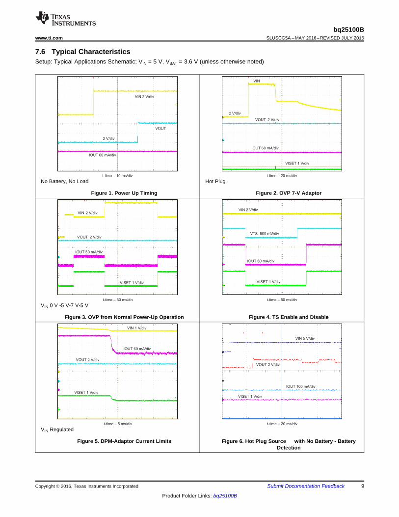
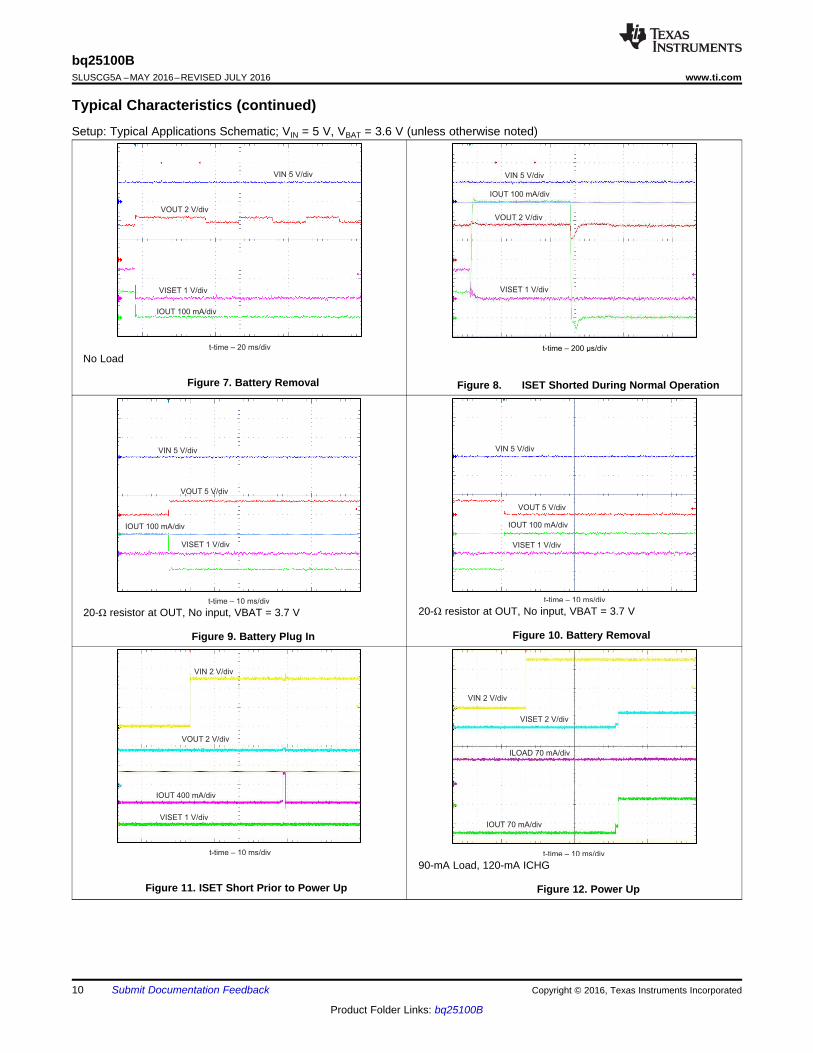
7.6 Typical CharacteristicsSetup: Typical Applications Schematic; VIN = 5 V, VBAT = 3.6 V (unless otherwise noted)
No Battery, No Load
Figure 1. Power Up Timing
Hot Plug
Figure 2. OVP 7-V Adaptor
VIN 0 V -5 V-7 V-5 V
Figure 3. OVP from Normal Power-Up Operation Figure 4. TS Enable and Disable
VIN Regulated
Figure 5. DPM-Adaptor Current Limits Figure 6. Hot Plug Source with No Battery - BatteryDetection
t-time – 10 ms/div
VISET 2 V/div
ILOAD 70 mA/div
IOUT 70 mA/div
VIN 2 V/div
t-time – 10 ms/div
VISET 1 V/div
VOUT 2 V/div
IOUT 400 mA/div
VIN 2 V/div
t-time – 10 ms/div
VISET 1 V/div
VOUT 5 V/div
IOUT 100 mA/div
VIN 5 V/div
t-time – 10 ms/div
VISET 1 V/div
VOUT 5 V/div
IOUT 100 mA/div
VIN 5 V/div
VISET 1 V/div
VOUT 2 V/div
IOUT 100 mA/div
VIN 5 V/div
t-time – 200 s/divμt-time – 20 ms/div
VISET 1 V/div
VOUT 2 V/div
IOUT 100 mA/div
VIN 5 V/div
10
bq25100BSLUSCG5A –MAY 2016–REVISED JULY 2016 www.ti.com
Product Folder Links: bq25100B
Submit Documentation Feedback Copyright © 2016, Texas Instruments Incorporated
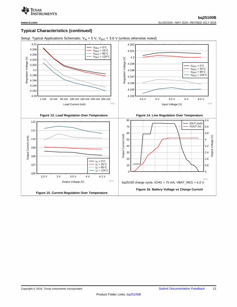
Typical Characteristics (continued)Setup: Typical Applications Schematic; VIN = 5 V, VBAT = 3.6 V (unless otherwise noted)
No Load
Figure 7. Battery Removal Figure 8. ISET Shorted During Normal Operation
20-Ω resistor at OUT, No input, VBAT = 3.7 V
Figure 9. Battery Plug In
20-Ω resistor at OUT, No input, VBAT = 3.7 V
Figure 10. Battery Removal
Figure 11. ISET Short Prior to Power Up
90-mA Load, 120-mA ICHG
Figure 12. Power Up
Output Voltage (V)
Out
put C
urre
nt (
mA
)
106
107
108
109
110
111
112
2.5 V 3 V 3.5 V 4 V 4.1 V
D003
IO = 0qCIO = 25qCIO = 85qCIO = 125qC
Out
put C
urre
nt (
mA
)
Out
put V
olta
ge (
V)
0 0
10 0.8
20 1.6
30 2.4
40 3.2
50 4
60 4.8
70 5.6
80 6.4
D004
IOUT (mA)VOUT (V)
Load Current (mA)
Reg
ulat
ion
Vol
tage
(V
)
4.19
4.192
4.194
4.196
4.198
4.2
4.202
4.204
4.206
4.208
4.21
1 mA 10 mA 50 mA 100 mA 150 mA 200 mA 250 mA
D001
VREG = 0qCVREG = 25qCVREG = 85qCVREG = 125qC
Input Voltage (V)
Reg
ulat
ion
Vol
tage
(V
)
4.194
4.195
4.196
4.197
4.198
4.199
4.2
4.201
4.202
4.5 V 5 V 5.5 V 6 V 6.5 V
D002
VREG = 0qCVREG = 25qCVREG = 85qCVREG = 125qC
11
bq25100Bwww.ti.com SLUSCG5A –MAY 2016–REVISED JULY 2016
Product Folder Links: bq25100B
Submit Documentation FeedbackCopyright © 2016, Texas Instruments Incorporated
Typical Characteristics (continued)Setup: Typical Applications Schematic; VIN = 5 V, VBAT = 3.6 V (unless otherwise noted)
Figure 13. Load Regulation Over Temperature Figure 14. Line Regulation Over Temperature
Figure 15. Current Regulation Over Temperature
bq25100 charge cycle, ICHG = 75 mA, VBAT_REG = 4.2 V
Figure 16. Battery Voltage vs Charge Current
12
bq25100BSLUSCG5A –MAY 2016–REVISED JULY 2016 www.ti.com
Product Folder Links: bq25100B
Submit Documentation Feedback Copyright © 2016, Texas Instruments Incorporated
8 Detailed Description
8.1 OverviewThe bq25100B is a highly integrated family of single cell Li-Ion and Li-Pol chargers. The charger can be used tocharge a battery, power a system or both. The charger has three phases of charging: pre-charge to recover afully discharged battery, fast-charge constant current to supply the charge safely and voltage regulation to safelyreach full capacity. The charger is very flexible, allowing programming of the fast-charge current and Pre-charge/Termination Current. This charger is designed to work with a USB connection (100-mA limit) or Adaptor(DC output). The charger also checks to see if a battery is present. The following discussion reviews all productsin the bq25100B family. Not all features apply to the bq25100B.
The charger also comes with a full set of safety features: JEITA Temperature Standard(bq25100/01/100H/101H), Over-Voltage Protection, DPM-IN, Safety Timers, and ISET short protection. All ofthese features and more are described in detail below.
The charger is designed for a single power path from the input to the output to charge a single cell Li-Ion orLi-Pol battery pack. Upon application of a 5-V DC power source the ISET and OUT short checks are performedto assure a proper charge cycle.
If the battery voltage is below the LOWV threshold, the battery is considered discharged and a preconditioningcycle begins. The amount of precharge current can be programmed using the PRE-TERM pin which programs apercent of fast charge current (10 to 100%) as the precharge current. This feature is useful when the system loadis connected across the battery “stealing” the battery current. The precharge current can be set higher to accountfor the system loading while allowing the battery to be properly conditioned. The PRE-TERM pin is a dualfunction pin which sets the precharge current level and the termination threshold level. The termination "currentthreshold" is always half of the precharge programmed current level.
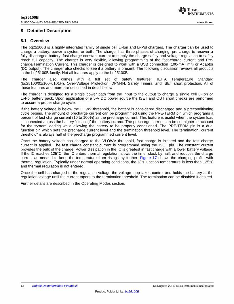
Once the battery voltage has charged to the VLOWV threshold, fast charge is initiated and the fast chargecurrent is applied. The fast charge constant current is programmed using the ISET pin. The constant currentprovides the bulk of the charge. Power dissipation in the IC is greatest in fast charge with a lower battery voltage.If the IC reaches 125°C, the IC enters thermal regulation, slows the timer clock by half, and reduces the chargecurrent as needed to keep the temperature from rising any further. Figure 17 shows the charging profile withthermal regulation. Typically under normal operating conditions, the IC’s junction temperature is less than 125°Cand thermal regulation is not entered.
Once the cell has charged to the regulation voltage the voltage loop takes control and holds the battery at theregulation voltage until the current tapers to the termination threshold. The termination can be disabled if desired.
Further details are described in the Operating Modes section.
PRE-CHARGECURRENT ANDTERMINATIONTHRESHOLD
FAST-CHARGECURRENT
T(PRECHG)
ChargeComplete
Status,Charger
Off
Pre-Conditioning
Phase
CurrentRegulation
Phase
Voltage Regulation andCharge Termination
Phase
BatteryVoltage,V(OUT)
Battery Current,I(OUT)
DONE
0A
ThermalRegulation
Phase
Temperature, Tj
IO(OUT)
T(THREG)
I(TERM)IO(PRECHG)
VO(REG)
VO(LOWV)
DONET(CHG)
13
bq25100Bwww.ti.com SLUSCG5A –MAY 2016–REVISED JULY 2016
Product Folder Links: bq25100B
Submit Documentation FeedbackCopyright © 2016, Texas Instruments Incorporated
Overview (continued)
Figure 17. Charging Profile With Thermal Regulation
+- 80 mV
OUT
ChargePump
Input Power Detect IN
IN-DPMREF
OUT
OUTREGREF
IN
OVPREF
TJ
125ÛCREF
IN
IN
ISET
ChargePump
PRE-TERMPA
CHARGECONTROL
OUTVTERM_EN
VCOLD-0ÛC
VHOT-60ÛC
VLDO
VDISABLE
TS
5PA 45PA
VCLAMP=1.4V
Cold Temperature Sink Current= 45PA
LO=LDO MODE
HI=CHIP DISABLE
OUT
+_
+_ +
_
+_
+_
+_
+_
+_
+_
+_
+_
+_
Internal Charge Current Sense
w/ Multiple Outputs
+_
Internal Current Sensing Resistor
22mA Startup Current Limit
+_
1.5V
FAST CHARGE
PRE-CHARGE
PRE-CHG Reference
Term Reference
+_
+_
150ÛCREF
Thermal Shutdown
TJ
+_
+_
VWARM-45ÛC
VCOOL-10ÛC
+_
Disable Sink Current = 20PA
Copyright © 2016, Texas Instruments Incorporated
14
bq25100BSLUSCG5A –MAY 2016–REVISED JULY 2016 www.ti.com
Product Folder Links: bq25100B
Submit Documentation Feedback Copyright © 2016, Texas Instruments Incorporated
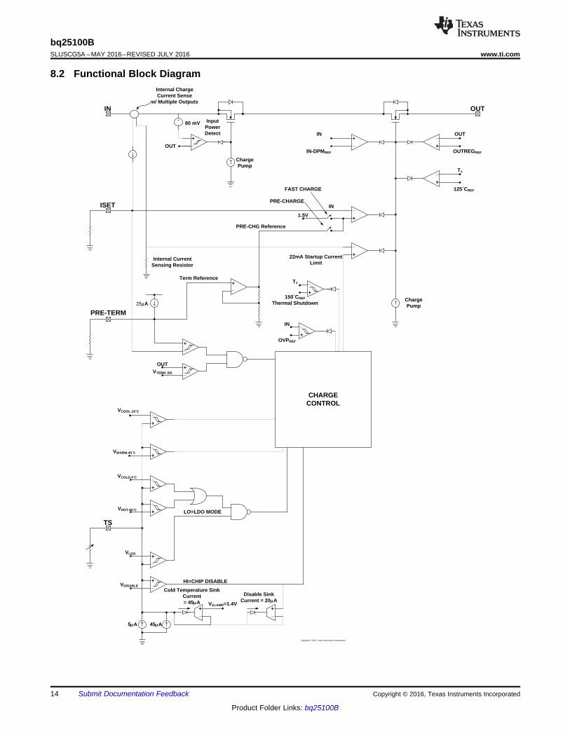
8.2 Functional Block Diagram
15
bq25100Bwww.ti.com SLUSCG5A –MAY 2016–REVISED JULY 2016
Product Folder Links: bq25100B
Submit Documentation FeedbackCopyright © 2016, Texas Instruments Incorporated
8.3 Feature Description
8.3.1 Overvoltage-Protection (OVP) – Continuously MonitoredIf the input source applies an overvoltage, the pass FET, if previously on, turns off after a deglitch, tBLK(OVP). Thetimer stops counting. Once the overvoltage returns to a normal voltage, the timer and charge continues.
8.3.2 CHG Pin Indication (bq25101, bq25101H)The charge pin has an internal open drain FET which is on (pulls down to VSS) during the first charge only(independent of TTDM) and is turned off once the battery reaches voltage regulation and the charge currenttapers to the termination threshold set by the PRE-TERM resistor. The bq25101/01H terminates at 10% of theprogrammed charge current. The charge pin is high impedance in sleep mode and OVP and returns to itsprevious state once the condition is removed. Cycling input power, removing and replacing the battery, pullingthe TS pin low and releasing or entering pre-charge mode causes the CHG pin to go reset (go low if power isgood and a discharged battery is attached) and is considered the start of a first charge.
8.3.3 CHG Pin LED Pull-up Source (bq25101, bq25101H)For host monitoring, a pull-up resistor is used between the CHG pin and the VCC of the host and for a visualindication a resistor in series with an LED is connected between the /CHG pin and a power source. If the CHGsource is capable of exceeding 7 V, a 6.2-V zener should be used to clamp the voltage. If the source is the OUTpin, note that as the battery changes voltage, and the brightness of the LEDs vary.
8.3.4 IN-DPM (VIN-DPM or IN-DPM)The IN-DPM feature is used to detect an input source voltage that is folding back (voltage dropping), reaching itscurrent limit due to excessive load. When the input voltage drops to the VIN-DPM threshold the internal pass FETstarts to reduce the current until there is no further drop in voltage at the input. This would prevent a source withvoltage less than VIN-DPM to power the out pin. This is an added safety feature that helps protect the source fromexcessive loads. This feature is not applicable for bq25100B.
8.3.5 OUTThe Charger’s OUT pin provides current to the battery and to the system, if present. This IC can be used tocharge the battery plus power the system, charge just the battery or just power the system (TTDM) assuming theloads do not exceed the available current. The OUT pin is a current limited source and is inherently protectedagainst shorts. If the system load ever exceeds the output programmed current threshold, the output will bedischarged unless there is sufficient capacitance or a charged battery present to supplement the excessive load.
8.3.6 ISETAn external resistor is used to Program the Output Current (10 to 250 mA) and can be used as a current monitor.
RISET = KISET ÷ IOUT (1)
Where:IOUT is the desired fast charge current;KISET is a gain factor found in the electrical specification
For greater accuracy at lower currents, part of the sense FET is disabled to give better resolution. Going fromhigher currents to low currents, there is hysteresis and the transition occurs around 50 mA.
The ISET resistor is short protected and will detect a resistance lower than ≉420 Ω. The detection requires atleast 50 mA of output current. If a “short” is detected, then the IC will latch off and can be reset by cycling thepower or cycling TS pin. The OUT current is internally clamped to a maximum current of 600 mA typical and isindependent of the ISET short detection circuitry.
For charge current that is below 50 mA, an extra RC circuit is recommended on ISET to acheive more stablecurrent signal. More detail is available in 9.1 Application Information.
VCOLDVCOOLVHOT
Programmed ICHG
(100%)
Programmed VBAT_REG
50%
Termination
DisableVWARM
0.20 0.4 0.6 0.8 1.0 1.2 1.4 1.6 1.8
Cold Fault
No Operation
During Cold FaultReduced VBAT_REG
TS Voltage-V
60C 45C 10C 0C
16
bq25100BSLUSCG5A –MAY 2016–REVISED JULY 2016 www.ti.com
Product Folder Links: bq25100B
Submit Documentation Feedback Copyright © 2016, Texas Instruments Incorporated
Feature Description (continued)
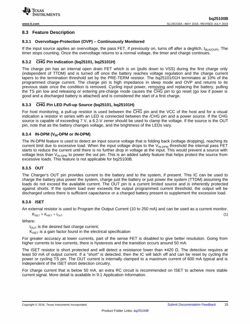
Figure 18. JEITA Operation Over TS Bias Voltage - bq25100, bq25100H, bq25101, bq25101H
VCOLDVCOOLVHOT
Programmed ICHG
(100%)
Programmed VBAT_REG
50%
Termination
DisableVWARM
0.20 0.4 0.6 0.8 1.0 1.2 1.4 1.6 1.8
Cold Fault
No Operation
During Cold FaultHot Fault
Charge Disable
TS Voltage-V
45C 10C 0C
17
bq25100Bwww.ti.com SLUSCG5A –MAY 2016–REVISED JULY 2016
Product Folder Links: bq25100B
Submit Documentation FeedbackCopyright © 2016, Texas Instruments Incorporated
Feature Description (continued)
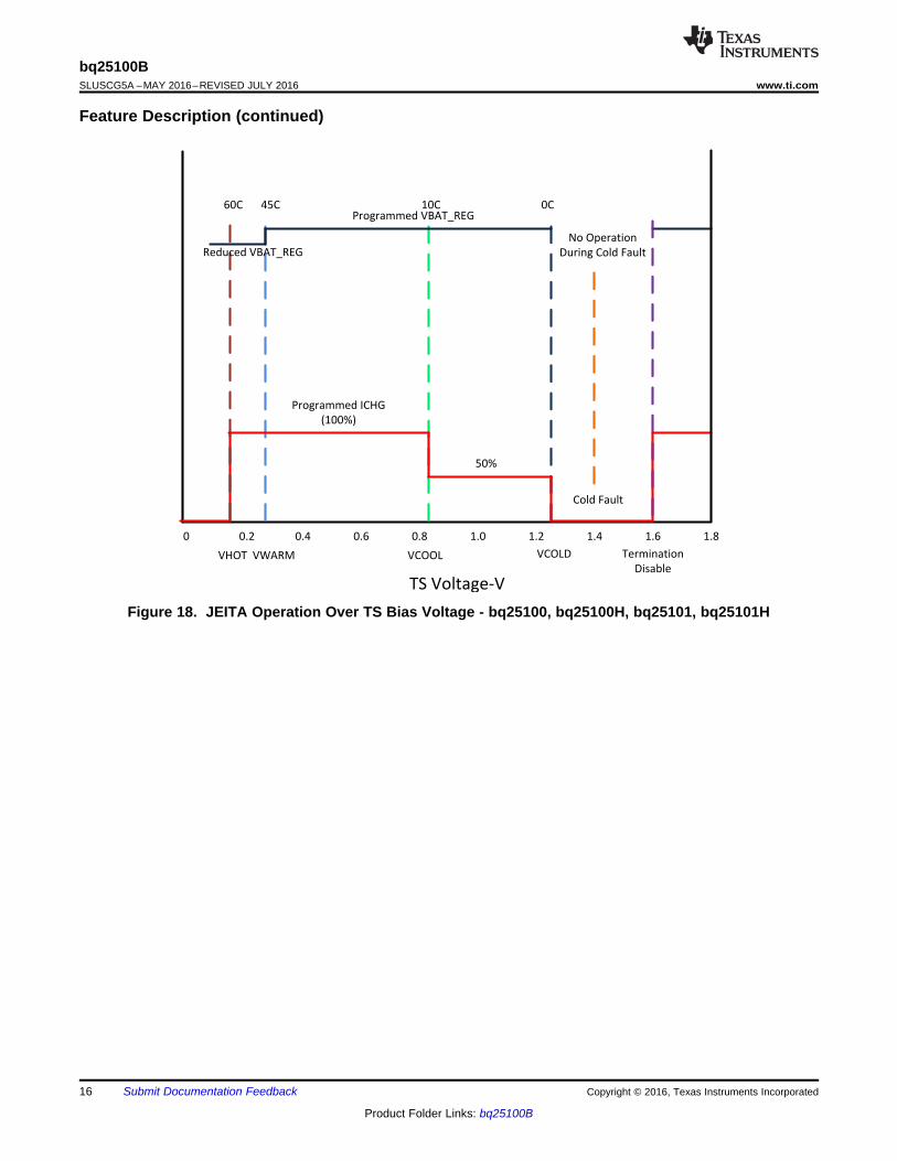
Figure 19. Standard Operation Over TS Bias Voltage – bq25100B, bq25100A, bq25100L
8.3.7 PRE_TERM – Pre-Charge and Termination Programmable ThresholdPre-Term is used to program both the pre-charge current and the termination current threshold. The pre-chargecurrent level is a factor of two higher than the termination current level. The termination can be set between 5and 50% (recommended range) of the programmed output current level set by ISET. If left floating thetermination and pre-charge are set internally at 10/20% respectively. The RPRE-TERM is ranged from 600 Ω to 30kΩ and the minimum termination current can be programmed to 1 mA. The pre-charge-to-fast-charge, Vlowvthreshold is set to 2.5 V.
RPRE-TERM = %Term × KTERM = %Pre-CHG × KPRE-CHG (2)
Where:%Term is the percent of fast charge current where termination occurs;%Pre-CHG is the percent of fast charge current that is desired during precharge;KTERM and KPRE-CHG are gain factors found in the electrical specifications.
8.3.8 TSThe TS function for the bq25100B/bq25100A cuts the charge current level in half between 0°C and 10°C anddisables charging when the NTC temperature is above 45°C. The TS function for thebq25100/bq25100H/bq25101/bq25101H is designed to follow the new JEITA temperature standard for Li-Ion andLi-Pol batteries. There are now four thresholds, 60°C, 45°C, 10°C, and 0°C. Normal operation occurs between10°C and 45°C. If between 0°C and 10°C the charge current level is cut in half and if between 45°C and 60°Cthe regulation voltage is reduced to 4.1 V max for bq25100 and 4.2 V max for bq25100H, see Figure 18.
18
bq25100BSLUSCG5A –MAY 2016–REVISED JULY 2016 www.ti.com
Product Folder Links: bq25100B
Submit Documentation Feedback Copyright © 2016, Texas Instruments Incorporated
Feature Description (continued)The TS feature is implemented using an internal 50μA current source to bias the thermistor (designed for usewith a 10-k NTC β = 3370 (SEMITEC 103AT-2 or Mitsubishi TH05-3H103F) connected from the TS pin to VSS. Ifthis feature is not needed, a fixed 10-k can be placed between TS and VSS to allow normal operation. This maybe done if the host is monitoring the thermistor and then the host would determine when to pull the TS pin low todisable charge.
The TS pin has two additional features, when the TS pin is pulled low or floated/driven high. A low disablescharge and a high puts the charger in TTDM.
Above 45°C (60°C for bq25100/bq25100H/bq25101/bq25101H) or below 0°C the charge is disabled. Once thethermistor reaches ≉–10°C the TS current folds back to keep a cold thermistor (between –10°C and –50°C) fromplacing the IC in the TTDM mode. If the TS pin is pulled low into disable mode, the current is reduce to ≉30 μA.Since the ITS curent is fixed along with the temperature thresholds, it is not possible to use thermistor valuesother than the 10-k NTC (at 25°C).
8.3.9 TimersThe pre-charge timer is set to 30 minutes. The pre-charge current, can be programmed to off-set any systemload, making sure that the 30 minutes is adequate.
The fast charge timer is fixed at 10 hours and can be increased real time by going into thermal regulation or IN-DPM. The timer clock slows by a factor of 2, resulting in a clock than counts half as fast when in these modes. Ifeither the 30 minute or ten hour timer times out, the charging is terminated and for bq25101/1H the CHG pingoes high impedance if not already in that state. The timer is reset by disabling the IC, cycling power or goinginto and out of TTDM.
8.3.10 TerminationOnce the OUT pin goes above VRCH, (reaches voltage regulation) and the current tapers down to thetermination threshold, a battery detect route is run to determine if the battery was removed or the battery is full. Ifthe battery is present, the charge current will terminate. If the battery was removed along with the thermistor,then the TS pin is driven high and the charge enters TTDM. If the battery was removed and the TS pin is held inthe active region, then the battery detect routine will continue until a battery is inserted. The termination currentcan be programmed down to 625 uA, however, the accuracy will reduce acoordingly when the terminationcurrent is below 1 mA.
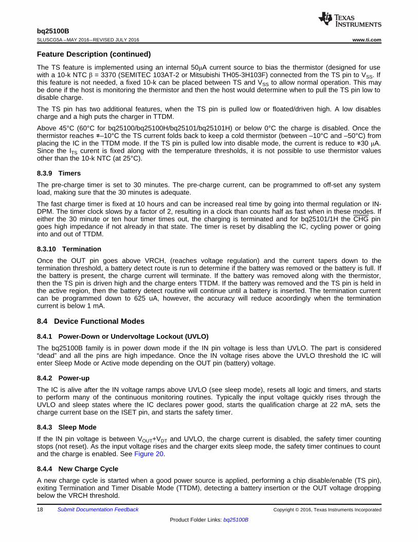
8.4 Device Functional Modes
8.4.1 Power-Down or Undervoltage Lockout (UVLO)The bq25100B family is in power down mode if the IN pin voltage is less than UVLO. The part is considered“dead” and all the pins are high impedance. Once the IN voltage rises above the UVLO threshold the IC willenter Sleep Mode or Active mode depending on the OUT pin (battery) voltage.
8.4.2 Power-upThe IC is alive after the IN voltage ramps above UVLO (see sleep mode), resets all logic and timers, and startsto perform many of the continuous monitoring routines. Typically the input voltage quickly rises through theUVLO and sleep states where the IC declares power good, starts the qualification charge at 22 mA, sets thecharge current base on the ISET pin, and starts the safety timer.
8.4.3 Sleep ModeIf the IN pin voltage is between VOUT+VDT and UVLO, the charge current is disabled, the safety timer countingstops (not reset). As the input voltage rises and the charger exits sleep mode, the safety timer continues to countand the charge is enabled. See Figure 20.
8.4.4 New Charge CycleA new charge cycle is started when a good power source is applied, performing a chip disable/enable (TS pin),exiting Termination and Timer Disable Mode (TTDM), detecting a battery insertion or the OUT voltage droppingbelow the VRCH threshold.
Is power good?
VBAT+VDT<VIN<VOVP
&VUVLO<VIN
Apply Input
Power
No
Is chip enabled?
VTS>VEN
Set Input Current Limit to 22mA
And Start Charge
Perform ISET & OUT short tests
Return to
Charge
No
Set charge current
based on ISET setting
Yes
Yes
19
bq25100Bwww.ti.com SLUSCG5A –MAY 2016–REVISED JULY 2016
Product Folder Links: bq25100B
Submit Documentation FeedbackCopyright © 2016, Texas Instruments Incorporated
Device Functional Modes (continued)
Figure 20. bq25100B Power-Up Flow Diagram
20
bq25100BSLUSCG5A –MAY 2016–REVISED JULY 2016 www.ti.com
Product Folder Links: bq25100B
Submit Documentation Feedback Copyright © 2016, Texas Instruments Incorporated
Device Functional Modes (continued)8.4.5 Termination and Timer Disable Mode (TTDM) - TS Pin HighThe battery charger is in TTDM when the TS pin goes high from removing the thermistor (removing batterypack/floating the TS pin) or by pulling the TS pin up to the TTDM threshold.
When entering TTDM, the 10 hour safety timer is held in reset and termination is disabled. A battery detectroutine is run to see if the battery was removed or not. For bq25101/1H, if the battery was removed then theCHG pin will go to its high impedance state if not already there. If a battery is detected the CHG pin does notchange states until the current tapers to the termination threshold, where the CHG pin goes to its highimpedance state if not already there (the regulated output will remain on).
The charging profile does not change (still has pre-charge, fast-charge constant current and constant voltagemodes). This implies the battery is still charged safely and the current is allowed to taper to zero.
When coming out of TTDM, the battery detect routine is run and if a battery is detected, then a new charge cyclebegins.
If TTDM is not desired upon removing the battery with the thermistor, one can add a 237-kΩ resistor between TSand VSS to disable TTDM. This keeps the current source from driving the TS pin into TTDM. This creates ≉0.1°Cerror at hot and a ≉3°C error at cold.
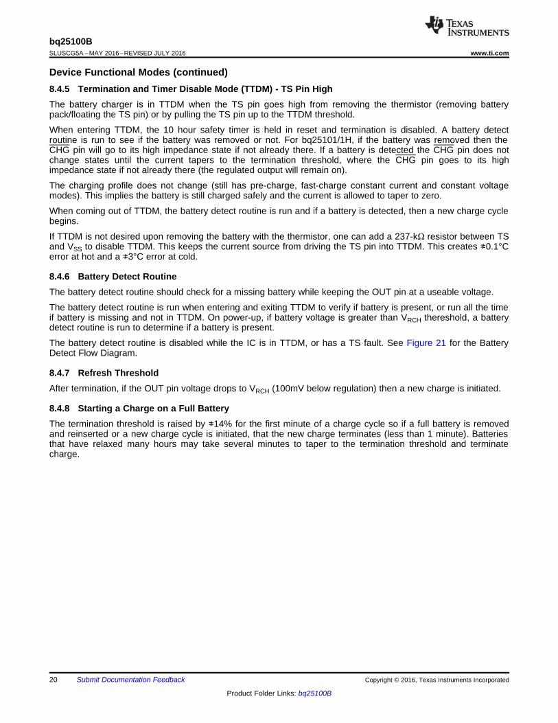
8.4.6 Battery Detect RoutineThe battery detect routine should check for a missing battery while keeping the OUT pin at a useable voltage.
The battery detect routine is run when entering and exiting TTDM to verify if battery is present, or run all the timeif battery is missing and not in TTDM. On power-up, if battery voltage is greater than VRCH thereshold, a batterydetect routine is run to determine if a battery is present.
The battery detect routine is disabled while the IC is in TTDM, or has a TS fault. See Figure 21 for the BatteryDetect Flow Diagram.
8.4.7 Refresh ThresholdAfter termination, if the OUT pin voltage drops to VRCH (100mV below regulation) then a new charge is initiated.
8.4.8 Starting a Charge on a Full BatteryThe termination threshold is raised by ≉14% for the first minute of a charge cycle so if a full battery is removedand reinserted or a new charge cycle is initiated, that the new charge terminates (less than 1 minute). Batteriesthat have relaxed many hours may take several minutes to taper to the termination threshold and terminatecharge.
Start
BATT_DETECT
Start 25ms timer
Timer Expired?
Is VOUT<VREG-100mV?
Battery Present
Turn off Sink Current
Return to flow
Set OUT REG
to VREG-400mV
Enable sink current
Reset & Start 25ms timer
No
Yes
Timer Expired?No
Yes
Is VOUT>VREG-300mV?
Battery Present
Turn off Sink Current
Return to flow
Yes
No
Yes
No
Battery Absent
Don’t Signal Charge
Turn off Sink Current
Return to Flow
21
bq25100Bwww.ti.com SLUSCG5A –MAY 2016–REVISED JULY 2016
Product Folder Links: bq25100B
Submit Documentation FeedbackCopyright © 2016, Texas Instruments Incorporated
Device Functional Modes (continued)
Figure 21. Battery Detect Routine
INVBUS
GND
HOST
bq25100B
OUT
1ÛF 1ÛF
SYSTEM
D+
D-
USB Port or Adapter
ISET
PRETERM
TEMPPACK+
PACK-
TS
VSS
CE
3.4k
6k
2.7k
10 nF
Optional RC
Copyright © 2016, Texas Instruments Incorporated
22
bq25100BSLUSCG5A –MAY 2016–REVISED JULY 2016 www.ti.com
Product Folder Links: bq25100B
Submit Documentation Feedback Copyright © 2016, Texas Instruments Incorporated
9 Application and Implementation
NOTEInformation in the following applications sections is not part of the TI componentspecification, and TI does not warrant its accuracy or completeness. TI’s customers areresponsible for determining suitability of components for their purposes. Customers shouldvalidate and test their design implementation to confirm system functionality.
9.1 Application InformationThe bq25100B series of devices are highly integrated Li-Ion and Li-Pol linear chargers targeted at space-limitedportable applications. The fast charge current can be programmed from 10 mA to 250 mA through an externalresistor on ISET pin. The pre_charge and termination current can also be programmed through the resistorconnected on PRETERM pin. The device has complete system-level protection such as input under-voltagelockout (UVLO), input over-voltage protection (OVP), sleep mode, thermal regulation, safety timers, and NTCmonitoring input.
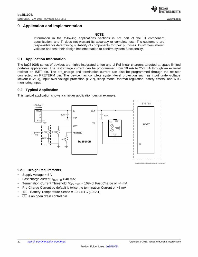
9.2 Typical ApplicationThis typical application shows a charger application design example.
9.2.1 Design Requirements• Supply voltage = 5 V• Fast charge current: IOUT-FC = 40 mA;• Termination Current Threshold: %IOUT-FC = 10% of Fast Charge or ~4 mA• Pre-Charge Current by default is twice the termination Current or ~8 mA• TS – Battery Temperature Sense = 10-k NTC (103AT)• CE is an open drain control pin
23
bq25100Bwww.ti.com SLUSCG5A –MAY 2016–REVISED JULY 2016
Product Folder Links: bq25100B
Submit Documentation FeedbackCopyright © 2016, Texas Instruments Incorporated
Typical Application (continued)9.2.2 Detailed Design Procedures• The regulation voltage is set to 4.2 V, the input voltage is 5 V and the charge current is programmed to 40
mA.• For charge current that is below 50 mA, an extra RC circuit is recommended on ISET to acheive more stable
current signal. For applications that need higher charge current, the RC circuit is not needed.• For applications that use more than 200-mA current, there could be a very low level ~1% of charge current
ringing in the output. The ringing can be removed by increasing the input capacitance.
9.2.2.1 Calculations
9.2.2.1.1 Program the Fast Charge Current, ISET:
RISET = [K(ISET) / I(OUT)]from electrical characteristics table. . . K(SET) = 135 AΩRISET = [135 AΩ/0.04 A] = 3.4 kΩSelecting the closest standard value, use a 3.4-kΩ resistor between ISET and Vss.
9.2.2.1.2 Program the Termination Current Threshold, ITERM:
RPRE-TERM = K(TERM) × %IOUT-FCRPRE-TERM = 600 Ω/% × 10% = 6 kΩSelecting the closest standard value, use a 6-kΩ resistor between PRETERM and Vss.One can arrive at the same value by using 20% for a pre-charge value (factor of 2 difference).RPRE-TERM = K(PRE-CHG) × %IOUT-FCRPRE-TERM = 300 Ω/% × 20%= 6 kΩ
9.2.2.1.3 TS Function
Use a 10-k NTC thermistor in the battery pack (103AT).
To Disable the temp sense function, use a fixed 10-kΩ resistor between the TS and VSS.
9.2.2.1.4 Selecting IN and OUT Pin Capacitors
In most applications, all that is needed is a high-frequency decoupling capacitor (ceramic) on the power pin, inputand output pins. Using the values shown on the application diagram is recommended. After evaluation of thesevoltage signals with real system operational conditions, one can determine if capacitance values can be adjustedtoward the minimum recommended values (DC load application) or higher values for fast, high amplitude, pulsedload applications. Note if designed for high input voltage sources (bad adaptors or wrong adaptors), the capacitorneeds to be rated appropriately. Ceramic capacitors are tested to 2x their rated values so a 16-V capacitor maybe adequate for a 30-V transient (verify tested rating with capacitor manufacturer).
t-time – 50 ms/div
VISET 1 V/div
VTS 500 mV/div
IOUT 60 mA/div
VIN 2 V/div
t-time – 10 ms/div
VISET 2 V/div
ILOAD 70 mA/div
IOUT 70 mA/div
VIN 2 V/div
t-time – 50 ms/div
VISET 1 V/div
2 V/div
VOUT
IOUT 60 mA/div
VIN
2 V/div
t-time – 20 ms/div
VISET 1 V/div
2 V/div
VOUT
IOUT 60 mA/div
VIN
2 V/div
24
bq25100BSLUSCG5A –MAY 2016–REVISED JULY 2016 www.ti.com
Product Folder Links: bq25100B
Submit Documentation Feedback Copyright © 2016, Texas Instruments Incorporated
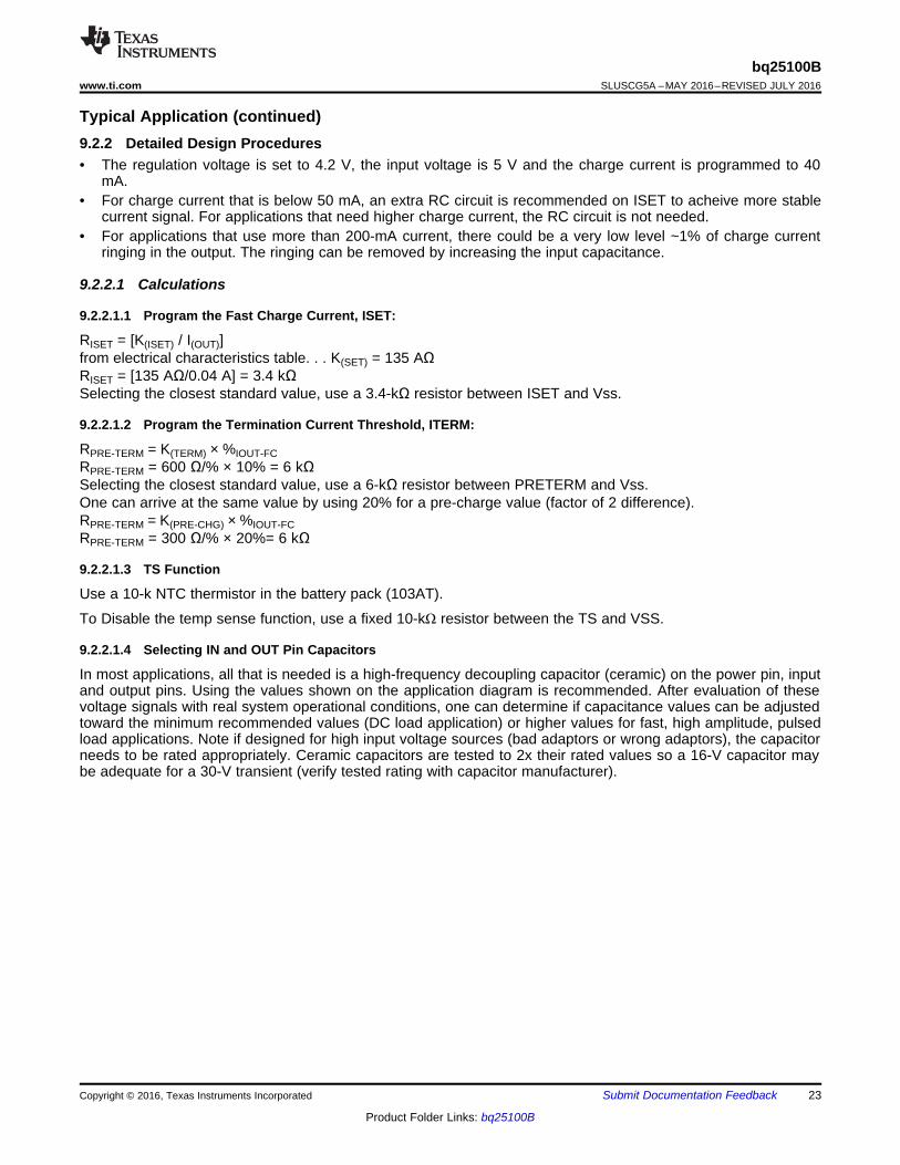
Typical Application (continued)9.2.3 Application Performance Plots
Hot Plug
Figure 22. OVP 7-V Adaptor
VIN 0 V -5 V-7 V-5 V
Figure 23. OVP from Normal Power-Up Operation
Figure 24. TS Enable and Disable
90-mA Load, 120-mA IOUT
Figure 25. Power Up
10 Power Supply Recommendations
10.1 Leakage Current Effects on Battery CapacityTo determine how fast a leakage current on the battery will discharge the battery is an easy calculation. The timefrom full to discharge can be calculated by dividing the Amp-Hour Capacity of the battery by the leakage current.For a 0.1-AHr battery and a 75-nA leakage current (100 mAHr/75 nA = 250000 Hours), it would take 1333k hoursor 152 years to discharge. In reality the self discharge of the cell would be much faster so the 75-nA leakagewould be considered negligible.
25
bq25100Bwww.ti.com SLUSCG5A –MAY 2016–REVISED JULY 2016
Product Folder Links: bq25100B
Submit Documentation FeedbackCopyright © 2016, Texas Instruments Incorporated
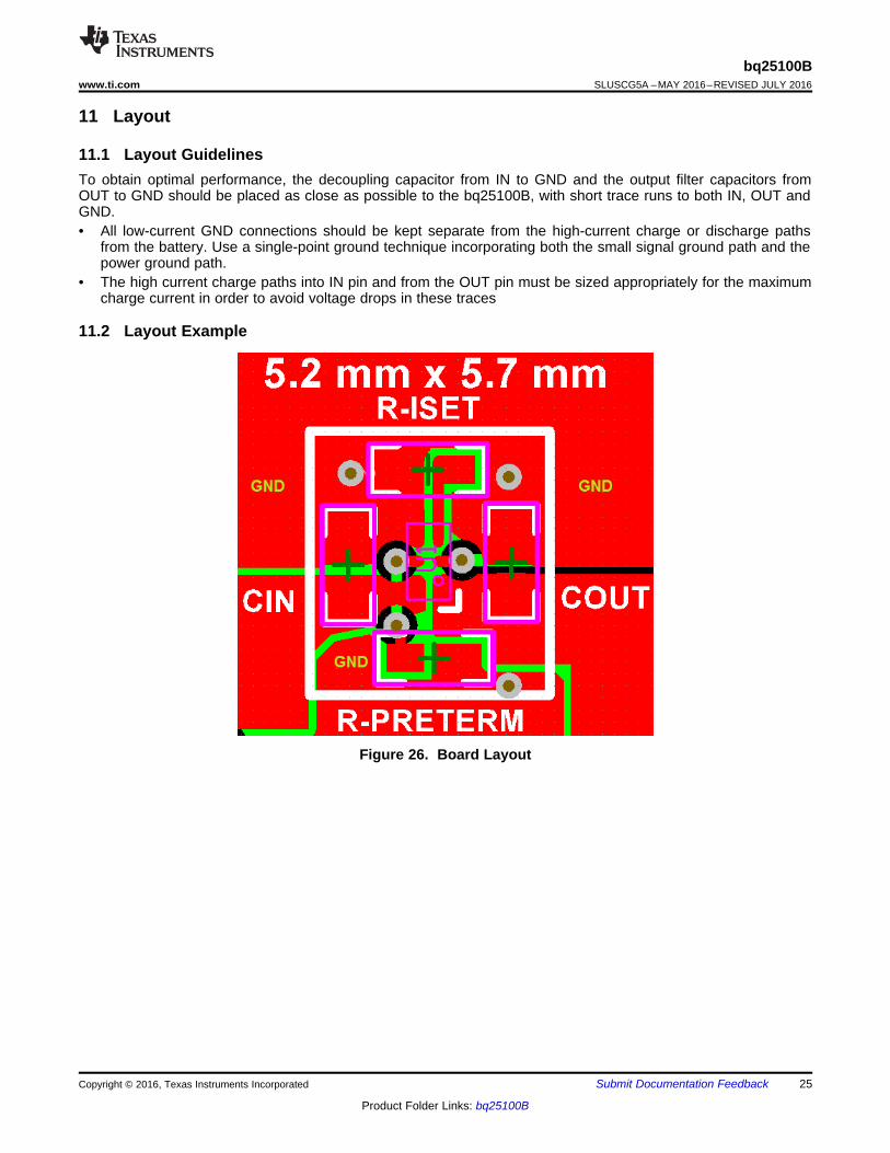
11 Layout
11.1 Layout GuidelinesTo obtain optimal performance, the decoupling capacitor from IN to GND and the output filter capacitors fromOUT to GND should be placed as close as possible to the bq25100B, with short trace runs to both IN, OUT andGND.• All low-current GND connections should be kept separate from the high-current charge or discharge paths
from the battery. Use a single-point ground technique incorporating both the small signal ground path and thepower ground path.
• The high current charge paths into IN pin and from the OUT pin must be sized appropriately for the maximumcharge current in order to avoid voltage drops in these traces
11.2 Layout Example
Figure 26. Board Layout
26
bq25100BSLUSCG5A –MAY 2016–REVISED JULY 2016 www.ti.com
Product Folder Links: bq25100B
Submit Documentation Feedback Copyright © 2016, Texas Instruments Incorporated
11.3 Thermal ConsiderationsThe most common measure of package thermal performance is thermal impedance (θJA ) measured (ormodeled) from the chip junction to the air surrounding the package surface (ambient). The mathematicalexpression for θJA is:
RθJA = (TJ – TA) / P
where• TJ = chip junction temperature• TA = Ambient temperature• P = device power dissipation (3)
Factors that can influence the measurement and calculation of RθJA include:1. Whether or not the device is board mounted2. Trace size, composition, thickness, and geometry3. Orientation of the device (horizontal or vertical)4. Volume of the ambient air surrounding the device under test and airflow5. Whether other surfaces are in close proximity to the device being tested
Due to the charge profile of Li-Ion and Li-Pol batteries the maximum power dissipation is typically seen at thebeginning of the charge cycle when the battery voltage is at its lowest. Typically after fast charge begins the packvoltage increases to ≉3.4 V within the first 2 minutes. The thermal time constant of the assembly typically takes afew minutes to heat up so when doing maximum power dissipation calculations, 3.4 V is a good minimum voltageto use.
The device power dissipation, P, is a function of the charge rate and the voltage drop across the internalPowerFET. It can be calculated from the following equation when a battery pack is being charged :
P = [V(IN) – V(OUT)] × I(OUT) (4)
The thermal loop feature reduces the charge current to limit excessive IC junction temperature. It isrecommended that the design not run in thermal regulation for typical operating conditions (nominal input voltageand nominal ambient temperatures) and use the feature for non typical situations such as hot environments orhigher than normal input source voltage. With that said, the IC will still perform as described, if the thermal loopis always active.
27
bq25100Bwww.ti.com SLUSCG5A –MAY 2016–REVISED JULY 2016
Product Folder Links: bq25100B
Submit Documentation FeedbackCopyright © 2016, Texas Instruments Incorporated
12 Device and Documentation Support
12.1 Device Support
12.1.1 Third-Party Products DisclaimerTI'S PUBLICATION OF INFORMATION REGARDING THIRD-PARTY PRODUCTS OR SERVICES DOES NOTCONSTITUTE AN ENDORSEMENT REGARDING THE SUITABILITY OF SUCH PRODUCTS OR SERVICESOR A WARRANTY, REPRESENTATION OR ENDORSEMENT OF SUCH PRODUCTS OR SERVICES, EITHERALONE OR IN COMBINATION WITH ANY TI PRODUCT OR SERVICE.
12.2 Related LinksThe table below lists quick access links. Categories include technical documents, support and communityresources, tools and software, and quick access to sample or buy.
Table 1. Related Links
PARTS PRODUCT FOLDER SAMPLE & BUY TECHNICALDOCUMENTS
TOOLS &SOFTWARE
SUPPORT &COMMUNITY
bq25100 Click here Click here Click here Click here Click herebq25101 Click here Click here Click here Click here Click here
bq25100A Click here Click here Click here Click here Click herebq25100H Click here Click here Click here Click here Click herebq25101H Click here Click here Click here Click here Click herebq25100L Click here Click here Click here Click here Click here
12.3 Receiving Notification of Documentation UpdatesTo receive notification of documentation updates, navigate to the device product folder on ti.com. In the upperright corner, click on Alert me to register and receive a weekly digest of any product information that haschanged. For change details, review the revision history included in any revised document.
12.4 Community ResourcesThe following links connect to TI community resources. Linked contents are provided "AS IS" by the respectivecontributors. They do not constitute TI specifications and do not necessarily reflect TI's views; see TI's Terms ofUse.
TI E2E™ Online Community TI's Engineer-to-Engineer (E2E) Community. Created to foster collaborationamong engineers. At e2e.ti.com, you can ask questions, share knowledge, explore ideas and helpsolve problems with fellow engineers.
Design Support TI's Design Support Quickly find helpful E2E forums along with design support tools andcontact information for technical support.
12.5 TrademarksE2E is a trademark of Texas Instruments.Bluetooth is a registered trademark of Bluetooth SIG, Inc..
12.6 Electrostatic Discharge CautionThese devices have limited built-in ESD protection. The leads should be shorted together or the device placed in conductive foamduring storage or handling to prevent electrostatic damage to the MOS gates.
12.7 GlossarySLYZ022 — TI Glossary.
This glossary lists and explains terms, acronyms, and definitions.
28
bq25100BSLUSCG5A –MAY 2016–REVISED JULY 2016 www.ti.com
Product Folder Links: bq25100B
Submit Documentation Feedback Copyright © 2016, Texas Instruments Incorporated
13 Mechanical, Packaging, and Orderable InformationThe following pages include mechanical, packaging, and orderable information. This information is the mostcurrent data available for the designated devices. This data is subject to change without notice and revision ofthis document. For browser-based versions of this data sheet, refer to the left-hand navigation.
PACKAGE OPTION ADDENDUM
www.ti.com 22-Jun-2016
Addendum-Page 1
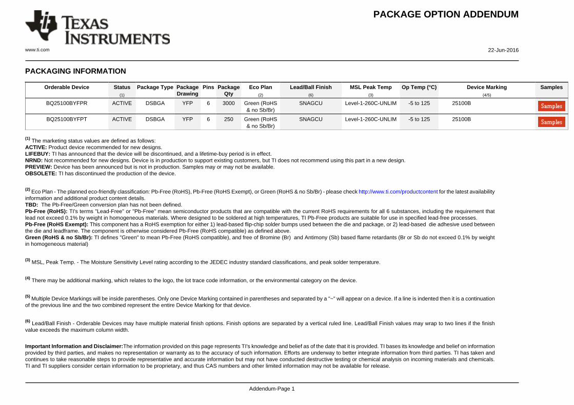
PACKAGING INFORMATION
Orderable Device Status(1)
Package Type PackageDrawing
Pins PackageQty
Eco Plan(2)
Lead/Ball Finish(6)
MSL Peak Temp(3)
Op Temp (°C) Device Marking(4/5)
Samples
BQ25100BYFPR ACTIVE DSBGA YFP 6 3000 Green (RoHS& no Sb/Br)
SNAGCU Level-1-260C-UNLIM -5 to 125 25100B
BQ25100BYFPT ACTIVE DSBGA YFP 6 250 Green (RoHS& no Sb/Br)
SNAGCU Level-1-260C-UNLIM -5 to 125 25100B
(1) The marketing status values are defined as follows:ACTIVE: Product device recommended for new designs.LIFEBUY: TI has announced that the device will be discontinued, and a lifetime-buy period is in effect.NRND: Not recommended for new designs. Device is in production to support existing customers, but TI does not recommend using this part in a new design.PREVIEW: Device has been announced but is not in production. Samples may or may not be available.OBSOLETE: TI has discontinued the production of the device.
(2) Eco Plan - The planned eco-friendly classification: Pb-Free (RoHS), Pb-Free (RoHS Exempt), or Green (RoHS & no Sb/Br) - please check http://www.ti.com/productcontent for the latest availabilityinformation and additional product content details.TBD: The Pb-Free/Green conversion plan has not been defined.Pb-Free (RoHS): TI's terms "Lead-Free" or "Pb-Free" mean semiconductor products that are compatible with the current RoHS requirements for all 6 substances, including the requirement thatlead not exceed 0.1% by weight in homogeneous materials. Where designed to be soldered at high temperatures, TI Pb-Free products are suitable for use in specified lead-free processes.Pb-Free (RoHS Exempt): This component has a RoHS exemption for either 1) lead-based flip-chip solder bumps used between the die and package, or 2) lead-based die adhesive used betweenthe die and leadframe. The component is otherwise considered Pb-Free (RoHS compatible) as defined above.Green (RoHS & no Sb/Br): TI defines "Green" to mean Pb-Free (RoHS compatible), and free of Bromine (Br) and Antimony (Sb) based flame retardants (Br or Sb do not exceed 0.1% by weightin homogeneous material)
(3) MSL, Peak Temp. - The Moisture Sensitivity Level rating according to the JEDEC industry standard classifications, and peak solder temperature.
(4) There may be additional marking, which relates to the logo, the lot trace code information, or the environmental category on the device.
(5) Multiple Device Markings will be inside parentheses. Only one Device Marking contained in parentheses and separated by a "~" will appear on a device. If a line is indented then it is a continuationof the previous line and the two combined represent the entire Device Marking for that device.
(6) Lead/Ball Finish - Orderable Devices may have multiple material finish options. Finish options are separated by a vertical ruled line. Lead/Ball Finish values may wrap to two lines if the finishvalue exceeds the maximum column width.
Important Information and Disclaimer:The information provided on this page represents TI's knowledge and belief as of the date that it is provided. TI bases its knowledge and belief on informationprovided by third parties, and makes no representation or warranty as to the accuracy of such information. Efforts are underway to better integrate information from third parties. TI has taken andcontinues to take reasonable steps to provide representative and accurate information but may not have conducted destructive testing or chemical analysis on incoming materials and chemicals.TI and TI suppliers consider certain information to be proprietary, and thus CAS numbers and other limited information may not be available for release.
PACKAGE OPTION ADDENDUM
www.ti.com 22-Jun-2016
Addendum-Page 2
In no event shall TI's liability arising out of such information exceed the total purchase price of the TI part(s) at issue in this document sold by TI to Customer on an annual basis.
TAPE AND REEL INFORMATION
*All dimensions are nominal
Device PackageType
PackageDrawing
Pins SPQ ReelDiameter
(mm)
ReelWidth
W1 (mm)
A0(mm)
B0(mm)
K0(mm)
P1(mm)
W(mm)
Pin1Quadrant
BQ25100BYFPR DSBGA YFP 6 3000 180.0 8.4 0.98 1.68 0.59 4.0 8.0 Q1
BQ25100BYFPT DSBGA YFP 6 250 180.0 8.4 0.98 1.68 0.59 4.0 8.0 Q1
PACKAGE MATERIALS INFORMATION
www.ti.com 19-Jul-2016
Pack Materials-Page 1
*All dimensions are nominal
Device Package Type Package Drawing Pins SPQ Length (mm) Width (mm) Height (mm)
BQ25100BYFPR DSBGA YFP 6 3000 210.0 185.0 35.0
BQ25100BYFPT DSBGA YFP 6 250 210.0 185.0 35.0
PACKAGE MATERIALS INFORMATION
www.ti.com 19-Jul-2016
Pack Materials-Page 2
www.ti.com
PACKAGE OUTLINE
C0.5 MAX
0.190.13
0.8TYP
0.4TYP
0.4 TYP
6X 0.250.21
B E A
D
4223410/A 11/2016
DSBGA - 0.5 mm max heightYFP0006DIE SIZE BALL GRID ARRAY
NOTES: 1. All linear dimensions are in millimeters. Any dimensions in parenthesis are for reference only. Dimensioning and tolerancing per ASME Y14.5M. 2. This drawing is subject to change without notice.
BALL A1CORNER
SEATING PLANE
BALL TYP 0.05 C
A
B
C
20.015 C A B
SYMM
SYMM
1
SCALE 10.000
D: Max =
E: Max =
1.608 mm, Min =
0.91 mm, Min =
1.547 mm
0.85 mm
www.ti.com
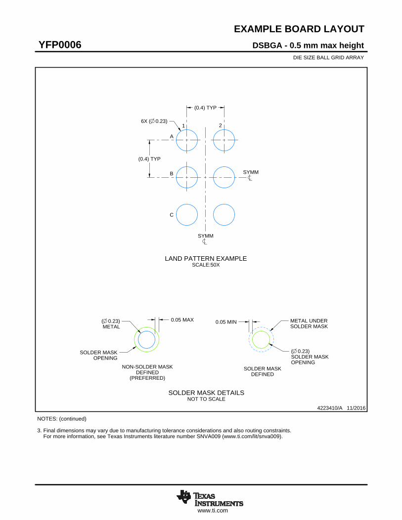
EXAMPLE BOARD LAYOUT
6X ( 0.23)
(0.4) TYP
(0.4) TYP
( 0.23)METAL
0.05 MAX
SOLDER MASKOPENING
METAL UNDERSOLDER MASK
( 0.23)SOLDER MASKOPENING
0.05 MIN
4223410/A 11/2016
DSBGA - 0.5 mm max heightYFP0006DIE SIZE BALL GRID ARRAY
NOTES: (continued) 3. Final dimensions may vary due to manufacturing tolerance considerations and also routing constraints. For more information, see Texas Instruments literature number SNVA009 (www.ti.com/lit/snva009).
SOLDER MASK DETAILSNOT TO SCALE
SYMM
SYMM
LAND PATTERN EXAMPLESCALE:50X
A
B
C
1 2
NON-SOLDER MASKDEFINED
(PREFERRED)
SOLDER MASKDEFINED
www.ti.com
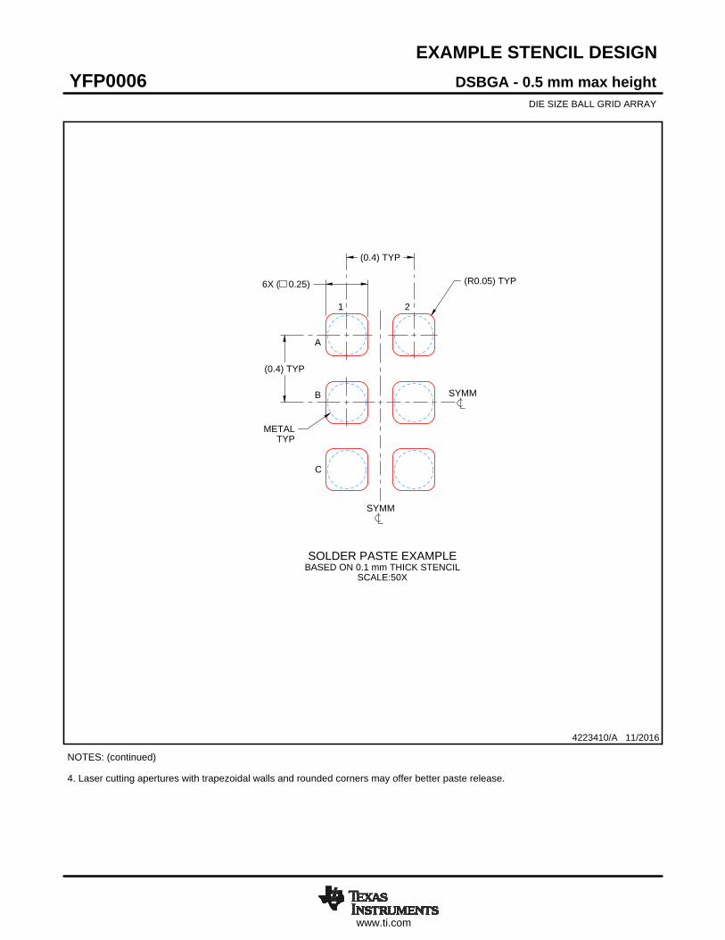
EXAMPLE STENCIL DESIGN
(0.4) TYP
(0.4) TYP
6X ( 0.25) (R0.05) TYP
METALTYP
4223410/A 11/2016
DSBGA - 0.5 mm max heightYFP0006DIE SIZE BALL GRID ARRAY
NOTES: (continued) 4. Laser cutting apertures with trapezoidal walls and rounded corners may offer better paste release.
SYMM
SYMM
SOLDER PASTE EXAMPLEBASED ON 0.1 mm THICK STENCIL
SCALE:50X
A
B
C
1 2
IMPORTANT NOTICE
Texas Instruments Incorporated (TI) reserves the right to make corrections, enhancements, improvements and other changes to itssemiconductor products and services per JESD46, latest issue, and to discontinue any product or service per JESD48, latest issue. Buyersshould obtain the latest relevant information before placing orders and should verify that such information is current and complete.TI’s published terms of sale for semiconductor products (http://www.ti.com/sc/docs/stdterms.htm) apply to the sale of packaged integratedcircuit products that TI has qualified and released to market. Additional terms may apply to the use or sale of other types of TI products andservices.Reproduction of significant portions of TI information in TI data sheets is permissible only if reproduction is without alteration and isaccompanied by all associated warranties, conditions, limitations, and notices. TI is not responsible or liable for such reproduceddocumentation. Information of third parties may be subject to additional restrictions. Resale of TI products or services with statementsdifferent from or beyond the parameters stated by TI for that product or service voids all express and any implied warranties for theassociated TI product or service and is an unfair and deceptive business practice. TI is not responsible or liable for any such statements.Buyers and others who are developing systems that incorporate TI products (collectively, “Designers”) understand and agree that Designersremain responsible for using their independent analysis, evaluation and judgment in designing their applications and that Designers havefull and exclusive responsibility to assure the safety of Designers' applications and compliance of their applications (and of all TI productsused in or for Designers’ applications) with all applicable regulations, laws and other applicable requirements. Designer represents that, withrespect to their applications, Designer has all the necessary expertise to create and implement safeguards that (1) anticipate dangerousconsequences of failures, (2) monitor failures and their consequences, and (3) lessen the likelihood of failures that might cause harm andtake appropriate actions. Designer agrees that prior to using or distributing any applications that include TI products, Designer willthoroughly test such applications and the functionality of such TI products as used in such applications.TI’s provision of technical, application or other design advice, quality characterization, reliability data or other services or information,including, but not limited to, reference designs and materials relating to evaluation modules, (collectively, “TI Resources”) are intended toassist designers who are developing applications that incorporate TI products; by downloading, accessing or using TI Resources in anyway, Designer (individually or, if Designer is acting on behalf of a company, Designer’s company) agrees to use any particular TI Resourcesolely for this purpose and subject to the terms of this Notice.TI’s provision of TI Resources does not expand or otherwise alter TI’s applicable published warranties or warranty disclaimers for TIproducts, and no additional obligations or liabilities arise from TI providing such TI Resources. TI reserves the right to make corrections,enhancements, improvements and other changes to its TI Resources. TI has not conducted any testing other than that specificallydescribed in the published documentation for a particular TI Resource.Designer is authorized to use, copy and modify any individual TI Resource only in connection with the development of applications thatinclude the TI product(s) identified in such TI Resource. NO OTHER LICENSE, EXPRESS OR IMPLIED, BY ESTOPPEL OR OTHERWISETO ANY OTHER TI INTELLECTUAL PROPERTY RIGHT, AND NO LICENSE TO ANY TECHNOLOGY OR INTELLECTUAL PROPERTYRIGHT OF TI OR ANY THIRD PARTY IS GRANTED HEREIN, including but not limited to any patent right, copyright, mask work right, orother intellectual property right relating to any combination, machine, or process in which TI products or services are used. Informationregarding or referencing third-party products or services does not constitute a license to use such products or services, or a warranty orendorsement thereof. Use of TI Resources may require a license from a third party under the patents or other intellectual property of thethird party, or a license from TI under the patents or other intellectual property of TI.TI RESOURCES ARE PROVIDED “AS IS” AND WITH ALL FAULTS. TI DISCLAIMS ALL OTHER WARRANTIES ORREPRESENTATIONS, EXPRESS OR IMPLIED, REGARDING RESOURCES OR USE THEREOF, INCLUDING BUT NOT LIMITED TOACCURACY OR COMPLETENESS, TITLE, ANY EPIDEMIC FAILURE WARRANTY AND ANY IMPLIED WARRANTIES OFMERCHANTABILITY, FITNESS FOR A PARTICULAR PURPOSE, AND NON-INFRINGEMENT OF ANY THIRD PARTY INTELLECTUALPROPERTY RIGHTS. TI SHALL NOT BE LIABLE FOR AND SHALL NOT DEFEND OR INDEMNIFY DESIGNER AGAINST ANY CLAIM,INCLUDING BUT NOT LIMITED TO ANY INFRINGEMENT CLAIM THAT RELATES TO OR IS BASED ON ANY COMBINATION OFPRODUCTS EVEN IF DESCRIBED IN TI RESOURCES OR OTHERWISE. IN NO EVENT SHALL TI BE LIABLE FOR ANY ACTUAL,DIRECT, SPECIAL, COLLATERAL, INDIRECT, PUNITIVE, INCIDENTAL, CONSEQUENTIAL OR EXEMPLARY DAMAGES INCONNECTION WITH OR ARISING OUT OF TI RESOURCES OR USE THEREOF, AND REGARDLESS OF WHETHER TI HAS BEENADVISED OF THE POSSIBILITY OF SUCH DAMAGES.Unless TI has explicitly designated an individual product as meeting the requirements of a particular industry standard (e.g., ISO/TS 16949and ISO 26262), TI is not responsible for any failure to meet such industry standard requirements.Where TI specifically promotes products as facilitating functional safety or as compliant with industry functional safety standards, suchproducts are intended to help enable customers to design and create their own applications that meet applicable functional safety standardsand requirements. Using products in an application does not by itself establish any safety features in the application. Designers mustensure compliance with safety-related requirements and standards applicable to their applications. Designer may not use any TI products inlife-critical medical equipment unless authorized officers of the parties have executed a special contract specifically governing such use.Life-critical medical equipment is medical equipment where failure of such equipment would cause serious bodily injury or death (e.g., lifesupport, pacemakers, defibrillators, heart pumps, neurostimulators, and implantables). Such equipment includes, without limitation, allmedical devices identified by the U.S. Food and Drug Administration as Class III devices and equivalent classifications outside the U.S.TI may expressly designate certain products as completing a particular qualification (e.g., Q100, Military Grade, or Enhanced Product).Designers agree that it has the necessary expertise to select the product with the appropriate qualification designation for their applicationsand that proper product selection is at Designers’ own risk. Designers are solely responsible for compliance with all legal and regulatoryrequirements in connection with such selection.Designer will fully indemnify TI and its representatives against any damages, costs, losses, and/or liabilities arising out of Designer’s non-compliance with the terms and provisions of this Notice.
Mailing Address: Texas Instruments, Post Office Box 655303, Dallas, Texas 75265Copyright © 2017, Texas Instruments Incorporated