Embed Size (px)
Citation preview

Battery
pack
SYSTEM
ACP ACN
ACDRV BATDRV
HIDRV
LODRV
PH
SRN
SRP
VFB
CE
VREF
ISET1
ISET2
ACSET
TTC
ADAPTER
ADAPTER
STAT1
STAT2
PG
VREF
TS
bq24630
Product
Folder
Sample &Buy
Technical
Documents
Tools &
Software
Support &Community
bq24630SLUS894B –JANUARY 2010–REVISED JULY 2015
bq24630 Standalone Synchronous Switched-Mode Lithium Phosphate Battery ChargerWith System Power Selector and Low Iq
1 Features 2 Applications1• 300-kHz NMOS-NMOS Synchronous Buck • Power Tool and Portable Equipment
Converter • Personal Digital Assistants• Stand-Alone Charger Specifically for Lithium • Handheld Terminals
Phosphate • Industrial and Medical Equipment• 5-V–28-V VCC Input Operating Range, Supports • Netbook, Mobile Internet Device, and Ultra-Mobile
1–7 Battery Cells PC• High-Accuracy Voltage and Current Regulation
3 Description– ±0.5% Charge Voltage AccuracyThe bq24630 is a highly integrated lithium phosphate– ±3% Charge Current Accuracyswitched-mode battery charge controller. The device– ±3% Adapter Current Accuracy offers a constant-frequency synchronous switching
• Integration PWM controller with high-accuracy charge currentand voltage regulation, charge preconditioning,– Automatic System Power Selection Fromtermination, adapter current regulation, and chargeAdapter or Batterystatus monitoring.– Internal Loop CompensationThe bq24630 charges the battery in three phases:– Internal Soft Startpreconditioning, constant current, and constant– Dynamic Power Management (DPM) voltage. Charge is terminated when the current
• Safety Protection reaches a minimum user-selectable level. Aprogrammable charge timer provides a safety– Input Overvoltage Protectionbackup. The bq24630 automatically restarts the– Battery Thermistor Sense Suspend Charge at charge cycle if the battery voltage falls below anHot/Cold and Automatically ICHARGE/8 at internal threshold and enters a low quiescent current
Hot/Cold or Warm/Cool sleep mode when the input voltage falls below the– Battery Detection battery voltage.– Reverse Protection Input FET
Device Information(1)– Programmable Safety Timer
PART NUMBER PACKAGE BODY SIZE (NOM)– Charge Overcurrent Protection
bq24630 VQFN (24) 4.00 mm × 4.00 mm– Battery Short Protection
(1) For all available packages, see the orderable addendum at– Battery Overvoltage Protection the end of the data sheet.– Thermal Shutdown
Simplified Schematic• Status Outputs– Adapter Present– Charger Operation Status
• Charge Enable Pin• 6-V Gate Drive for Synchronous Buck Converter• 30-ns Driver Dead Time and 99.95% Max.
Effective Duty Cycle• 24-Pin 4-mm × 4-mm QFN Package• Energy Star Low Quiescent Current Iq
– < 15-μA Off-State Battery Discharge Current– < 1.5-mA Off-State Input Quiescent Current
1
An IMPORTANT NOTICE at the end of this data sheet addresses availability, warranty, changes, use in safety-critical applications,intellectual property matters and other important disclaimers. PRODUCTION DATA.
bq24630SLUS894B –JANUARY 2010–REVISED JULY 2015 www.ti.com
Table of Contents8.4 Device Functional Modes........................................ 241 Features .................................................................. 1
9 Application and Implementation ........................ 252 Applications ........................................................... 19.1 Application Information............................................ 253 Description ............................................................. 19.2 Typical Application ................................................. 254 Revision History..................................................... 2
10 Power Supply Recommendations ..................... 305 Device Comparison Table ..................................... 311 Layout................................................................... 306 Pin Configuration and Functions ......................... 3
11.1 Layout Guidelines ................................................. 307 Specifications......................................................... 411.2 Layout Example .................................................... 317.1 Absolute Maximum Ratings ...................................... 4
12 Device and Documentation Support ................. 327.2 ESD Ratings ............................................................ 512.1 Device Support...................................................... 327.3 Recommended Operating Conditions....................... 512.2 Documentation Support ........................................ 327.4 Thermal Information .................................................. 512.3 Community Resources.......................................... 327.5 Electrical Characteristics........................................... 512.4 Trademarks ........................................................... 327.6 Typical Characteristics ............................................ 1012.5 Electrostatic Discharge Caution............................ 328 Detailed Description ............................................ 1312.6 Glossary ................................................................ 328.1 Overview ................................................................. 13
13 Mechanical, Packaging, and Orderable8.2 Functional Block Diagram ....................................... 14Information ........................................................... 328.3 Feature Description................................................. 15
4 Revision History
Changes from Revision A (October 2011) to Revision B Page
• Added ESD Ratings table, Feature Description section, Device Functional Modes, Application and Implementationsection, Power Supply Recommendations section, Layout section, Device and Documentation Support section, andMechanical, Packaging, and Orderable Information section .................................................................................................. 1
• Added text, equations and illustrations from Inductor Selection to PCB Layout .................................................................. 26
Changes from Original (January 2010) to Revision A Page
• Changed descriptions for PH and BTST pins......................................................................................................................... 4• Changed Equation 1 From: R1/R2 To: R2/R1...................................................................................................................... 15• Changed Equation 1 ............................................................................................................................................................ 15• Changed Equation 15 .......................................................................................................................................................... 26
2 Submit Documentation Feedback Copyright © 2010–2015, Texas Instruments Incorporated
Product Folder Links: bq24630

24 23 22 21 20 19
7 8 9 10 11 12
18
17
16
15
14
13
1
2
3
4
5
6
CE
ACN
ACP
ACDRV
STAT1
TS SRN
SRP
ISET 2
ACSET
GND
REGN
VC
C
BA
TD
RV
BT
ST
HID
RV
PH
LO
DR
V
TT
C
PG
STA
T2
VR
EF
ISE
T1
VF
B
OAT(bq24630)
QFN-24
bq24630www.ti.com SLUS894B –JANUARY 2010–REVISED JULY 2015
5 Device Comparison Table
bq24620 bq24630Cell chemistry Lithium phosphate Lithium phosphateNumber of cells in series (minimum to 1 to 7 1 to 7maximum, 4.2 V/cell)Charge voltage (minimum to maximum) (V) 1.8 to 26 1.8 to 26Input voltage range (minimum to maximum) (V) 5 to 28 5 to 28Input overvoltage (V) 32 32Maximum battery charging current (A) 10 10Switching frequency (kHz) 300 300JEITA charging temperature profile No NoDPM No IIN DPM
6 Pin Configuration and Functions
RGE Package24-Pin VQFN
Top View
Pin FunctionsPIN
I/O DESCRIPTIONNAME NO.
ACDRV 3 O AC adapter to system MOSFET driver output. Connect through a 1-kΩ resistor to the gate of the ACFET P-channel powerMOSFET and the reverse conduction blocking P-channel power MOSFET. The internal gate drive is asymmetrical, allowing aquick turnoff and slow turnon, in addition to the internal break-before-make logic with respect to BATDRV. If needed, anoptional capacitor from gate to source of the ACFET is used to slow down the ON and OFF times.
ACN 1 I Adapter-current sense resistor, negative input. A 0.1-μF ceramic capacitor is placed from ACN to ACP to provide differential-mode filtering. An optional 0.1-μF ceramic capacitor is placed from the ACN pin to GND for common-mode filtering.
ACP 2 I Adapter-current sense resistor, positive input. A 0.1-μF ceramic capacitor is placed from ACN to ACP to provide differential-mode filtering. A 0.1-μF ceramic capacitor is placed from the ACP pin to GND for common-mode filtering.
ACSET 16 I Adapter-current set input. The voltage of ACSET pin programs the input current regulation set-point during dynamic powermanagement (DPM).
BATDRV 23 O Battery-to-system MOSFET-driver output. Gate drive for the battery-to-system load BAT PMOS power FET to isolate thesystem from the battery to prevent current flow from the system to the battery, while allowing a low-impedance path frombattery to system. Connect this pin through a 1-kΩ resistor to the gate of the input BAT P-channel MOSFET. Connect thesource of the FET to the system load voltage node. Connect the drain of the FET to the battery pack positive terminal. Theinternal gate drive is asymmetrical to allow a quick turnoff and slow turnon, in addition to the internal break-before-make logicwith respect to ACDRV. If needed, an optional capacitor from gate to source of the BATFET is used to slow down the ON andOFF times.
BTST 22 – PWM high-side driver positive supply. Connect the 0.1-μF bootstrap capacitor from PH to BTST, and a bootstrap Schottkydiode from REGN to BTST.
CE 4 I Charge-enable active-HIGH logic input. HI enables charge. LO disables charge. It has an internal 1-MΩ pulldown resistor.
GND 17 – Low-current sensitive analog/digital ground. On PCB layout, connect with the thermal pad underneath the IC.
HIDRV 21 O PWM high-side driver output. Connect to the gate of the high-side power MOSFET with a short trace.
Copyright © 2010–2015, Texas Instruments Incorporated Submit Documentation Feedback 3
Product Folder Links: bq24630

bq24630SLUS894B –JANUARY 2010–REVISED JULY 2015 www.ti.com
Pin Functions (continued)PIN
I/O DESCRIPTIONNAME NO.
ISET1 11 I Fast-charge current-set input. The voltage of ISET1 pin programs the fast-charge current-regulation set point.
ISET2 15 I Termination-current set input. The voltage of ISET2 pin programs termination current trigger point.
LODRV 19 O PWM low-side driver output. Connect to the gate of the low-side power MOSFET with a short trace.
PG 8 O Open-drain power-good status output. Active-LOW when IC has a valid VCC (not in UVLO or ACOV or SLEEP mode). Active-HIGH when IC has an invalid VCC. PG can be used to drive an LED or communicate with a host processor.
PH 20 – PWM high-side driver negative supply. Connect to the phase-switching node (junction of the low-side power MOSFET drain,high-side power MOSFET source, and output inductor).
REGN 18 O PWM low-side driver positive 6-V supply output. Connect a 1-μF ceramic capacitor from REGN to the GND pin, close to theIC. Use for low-side driver and high-side driver bootstrap voltage by connecting a small-signal Schottky diode from REGN toBTST.
SRN 13 I Charge-current sense resistor, negative input. A 0.1-μF ceramic capacitor is placed from SRN to SRP to provide differential-mode filtering. An optional 0.1-μF ceramic capacitor is placed from the SRN pin to GND for common-mode filtering.
SRP 14 I Charge-current sense resistor, positive input. A 0.1-μF ceramic capacitor is placed from SRN to SRP to provide differential-mode filtering. A 0.1-μF ceramic capacitor is placed from the SRP pin to GND for common-mode filtering.
STAT1 5 – Open-drain charge-status pin to indicate various charger operations.
STAT2 9 – Open-drain charge-status pin to indicate various charger operations.
Thermal — – Exposed pad beneath the IC. Always solder the thermal pad to the board, and have vias on the thermal pad plane star-pad connecting to GND and ground plane for high-current power converter. It also serves as a thermal pad to dissipate the heat.
TS 6 I Temperature qualification voltage input for battery pack negative-temperature-coefficient thermistor. Program the hot and coldtemperature window with a resistor divider from VREF to TS to GND.
TTC 7 I SafetyTimer and termination control. Connect a capacitor from this node to GND to set the timer. When this input is LOW, thetimer and termination are disabled. When this input is HIGH, the timer is disabled but termination is allowed.
VCC 24 – IC power positive supply. Connect through a 10-Ω resistor to the common-source (diode-OR) point: source of high-side P-channel MOSFET and source of reverse-blocking P-channel power MOSFET. Place a 1-μF ceramic capacitor from VCC tothe GND pin close to the IC.
VFB 12 O Output-voltage analog feedback adjustment. Connect the output of a resistive voltage divider from the battery terminals to thisnode to adjust the output battery-regulation voltage.
VREF 10 O 3.3-V regulated voltage output. Place a 1-μF ceramic capacitor from VREF to the GND pin close to the IC. This voltage couldbe used for programming of voltage and current regulation and for programming the TS threshold.
7 Specifications
7.1 Absolute Maximum Ratingsover operating free-air temperature range (unless otherwise noted) (1) (2) (3)
MIN MAX UNITVCC, ACP, ACN, SRP, SRN, BATDRV, ACDRV, CE, STAT1, STAT2, PG –0.3 33 VPH –2 36 VVFB –0.3 16 V
Voltage rangeREGN, LODRV, ACSET, TS, TTC –0.3 7 VBTST, HIDRV with respect to GND –0.3 39 VVREF, ISET1, ISET2 –0.3 3.6 V
Maximum difference voltage ACP–ACN, SRP–SRN –0.5 0.5 VJunction temperature range, TJ –40 155 °CStorage temperature range, Tstg –55 155 °C
(1) Stresses beyond those listed under Absolute Maximum Ratings may cause permanent damage to the device. These are stress ratingsonly, and functional operation of the device at these or any other conditions beyond those indicated under Recommended OperatingConditions is not implied. Exposure to absolute-maximum-rated conditions for extended periods may affect device reliability.
(2) All voltages are with respect to GND if not specified. Currents are positive into, negative out of the specified terminal. Consult PackagingSection of the data book for thermal limitations and considerations of packages.
(3) Must have a series resistor between battery pack to VFB if Battery Pack voltage is expected to be greater than 16 V. Usually, theresistor divider top resistor takes care of this.
4 Submit Documentation Feedback Copyright © 2010–2015, Texas Instruments Incorporated
Product Folder Links: bq24630

bq24630www.ti.com SLUS894B –JANUARY 2010–REVISED JULY 2015
7.2 ESD RatingsVALUE UNIT
Human-body model (HBM), per ANSI/ESDA/JEDEC JS-001 (1) ±2000V(ESD) Electrostatic discharge VCharged-device model (CDM), per JEDEC specification JESD22- ±500C101 (2)
(1) JEDEC document JEP155 states that 500-V HBM allows safe manufacturing with a standard ESD control process.(2) JEDEC document JEP157 states that 250-V CDM allows safe manufacturing with a standard ESD control process.
7.3 Recommended Operating ConditionsMIN NOM MAX UNIT
Voltage range VCC, ACP, ACN, SRP, SRN, BATDRV, ACDRV, CE, STAT1, STAT2, –0.3 28 VPGPH –2 30 VVFB –0.3 14 VREGN, LODRV, ACSET, TS, TTC –0.3 6.5 VBTST, HIDRV with respect to GND –0.3 34 VISET1, ISET2 –0.3 3.3 VVREF 3.3 V
Maximum difference ACP–ACN, SRP–SRN –0.2 0.2 Vvoltage
TJ Junction temperature range 0 125 °C
7.4 Thermal Informationbq24630
THERMAL METRIC (1) RGE (VQFN) UNIT24 PINS
RθJA Junction-to-ambient thermal resistance 43 °C/WRθJCt(op) Junction-to-case (top) thermal resistance 54.3 °C/WRθJB Junction-to-board thermal resistance 20 °C/WψJT Junction-to-top characterization parameter 0.6 °C/WψJB Junction-to-board characterization parameter 19 °C/WRθJC(bot) Junction-to-case (bottom) thermal resistance 4 °C/W
(1) For more information about traditional and new thermal metrics, see the Semiconductor and IC Package Thermal Metrics applicationreport, SPRA953.
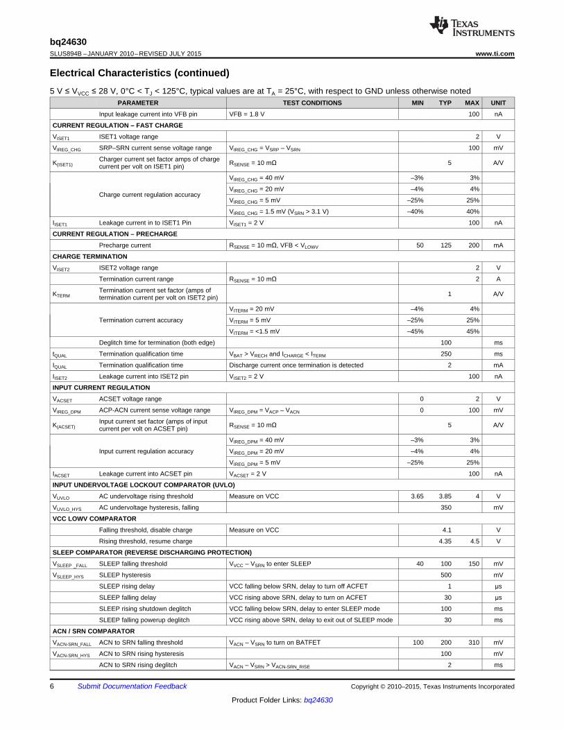
7.5 Electrical Characteristics5 V ≤ VVCC ≤ 28 V, 0°C < TJ < 125°C, typical values are at TA = 25°C, with respect to GND unless otherwise noted
PARAMETER TEST CONDITIONS MIN TYP MAX UNIT
OPERATING CONDITIONS
VVCC_OP VCC input voltage operating range 5 28 V
QUIESCENT CURRENTS
Total battery discharge current (sum ofcurrents into VCC, BTST, PH, ACP, ACN, VVCC < VSRN, VVCC > VUVLO (SLEEP) 15
μASRP, SRN, VFB), VFB ≤ 2.1 VIBAT
Battery discharge current (sum of currents VVCC > VSRN, VVCC > VUVLO CE = LOW 5into BTST, PH, SRP, SRN, VFB), VFB ≤
VVCC > VSRN, VVCC > VVCCLOW CE = HIGH, charge done 5 µA2.1 V
VVCC > VSRN, VVCC > VUVLO CE = LOW 1 1.5
Adapter supply current (current into VVCC > VSRN, VVCC > VVCCLOW , CE = HIGH, charge done 2 5IAC mAVCC,ACP,ACN pin) VVCC > VSRN, VVCC > VVCCLOW , CE = HIGH, charging, 12Qg_total = 20 nC, VVCC= 20 V
VFB Feedback regulation voltage 1.8 V
TJ = 0°C to 125°C –0.5% 0.5%Charge voltage regulation accuracy
TJ = –40°C to 125°C –0.7% 0.7%
Copyright © 2010–2015, Texas Instruments Incorporated Submit Documentation Feedback 5
Product Folder Links: bq24630
bq24630SLUS894B –JANUARY 2010–REVISED JULY 2015 www.ti.com
Electrical Characteristics (continued)5 V ≤ VVCC ≤ 28 V, 0°C < TJ < 125°C, typical values are at TA = 25°C, with respect to GND unless otherwise noted
PARAMETER TEST CONDITIONS MIN TYP MAX UNIT
Input leakage current into VFB pin VFB = 1.8 V 100 nA
CURRENT REGULATION – FAST CHARGE
VISET1 ISET1 voltage range 2 V
VIREG_CHG SRP–SRN current sense voltage range VIREG_CHG = VSRP – VSRN 100 mV
Charger current set factor amps of chargeK(ISET1) RSENSE = 10 mΩ 5 A/Vcurrent per volt on ISET1 pin)
VIREG_CHG = 40 mV –3% 3%
VIREG_CHG = 20 mV –4% 4%Charge current regulation accuracy
VIREG_CHG = 5 mV –25% 25%
VIREG_CHG = 1.5 mV (VSRN > 3.1 V) –40% 40%
IISET1 Leakage current in to ISET1 Pin VISET1 = 2 V 100 nA
CURRENT REGULATION – PRECHARGE
Precharge current RSENSE = 10 mΩ, VFB < VLOWV 50 125 200 mA
CHARGE TERMINATION
VISET2 ISET2 voltage range 2 V
Termination current range RSENSE = 10 mΩ 2 A
Termination current set factor (amps ofKTERM 1 A/Vtermination current per volt on ISET2 pin)
VITERM = 20 mV –4% 4%
Termination current accuracy VITERM = 5 mV –25% 25%
VITERM = <1.5 mV –45% 45%
Deglitch time for termination (both edge) 100 ms
tQUAL Termination qualification time VBAT > VRECH and ICHARGE < ITERM 250 ms
IQUAL Termination qualification time Discharge current once termination is detected 2 mA
IISET2 Leakage current into ISET2 pin VISET2 = 2 V 100 nA
INPUT CURRENT REGULATION
VACSET ACSET voltage range 0 2 V
VIREG_DPM ACP-ACN current sense voltage range VIREG_DPM = VACP – VACN 0 100 mV
Input current set factor (amps of inputK(ACSET) RSENSE = 10 mΩ 5 A/Vcurrent per volt on ACSET pin)
VIREG_DPM = 40 mV –3% 3%
Input current regulation accuracy VIREG_DPM = 20 mV –4% 4%
VIREG_DPM = 5 mV –25% 25%
IACSET Leakage current into ACSET pin VACSET = 2 V 100 nA
INPUT UNDERVOLTAGE LOCKOUT COMPARATOR (UVLO)
VUVLO AC undervoltage rising threshold Measure on VCC 3.65 3.85 4 V
VUVLO_HYS AC undervoltage hysteresis, falling 350 mV
VCC LOWV COMPARATOR
Falling threshold, disable charge Measure on VCC 4.1 V
Rising threshold, resume charge 4.35 4.5 V
SLEEP COMPARATOR (REVERSE DISCHARGING PROTECTION)
VSLEEP _FALL SLEEP falling threshold VVCC – VSRN to enter SLEEP 40 100 150 mV
VSLEEP_HYS SLEEP hysteresis 500 mV
SLEEP rising delay VCC falling below SRN, delay to turn off ACFET 1 μs
SLEEP falling delay VCC rising above SRN, delay to turn on ACFET 30 μs
SLEEP rising shutdown deglitch VCC falling below SRN, delay to enter SLEEP mode 100 ms
SLEEP falling powerup deglitch VCC rising above SRN, delay to exit out of SLEEP mode 30 ms
ACN / SRN COMPARATOR
VACN-SRN_FALL ACN to SRN falling threshold VACN – VSRN to turn on BATFET 100 200 310 mV
VACN-SRN_HYS ACN to SRN rising hysteresis 100 mV
ACN to SRN rising deglitch VACN – VSRN > VACN-SRN_RISE 2 ms
6 Submit Documentation Feedback Copyright © 2010–2015, Texas Instruments Incorporated
Product Folder Links: bq24630
bq24630www.ti.com SLUS894B –JANUARY 2010–REVISED JULY 2015
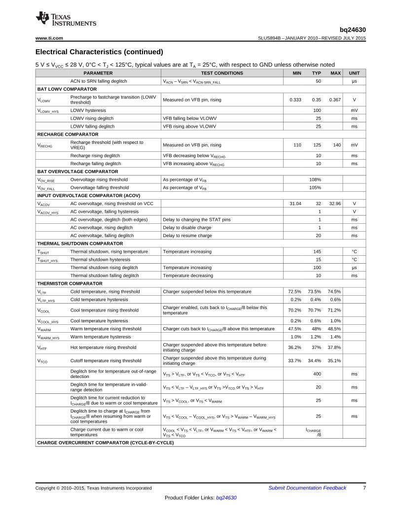
Electrical Characteristics (continued)5 V ≤ VVCC ≤ 28 V, 0°C < TJ < 125°C, typical values are at TA = 25°C, with respect to GND unless otherwise noted
PARAMETER TEST CONDITIONS MIN TYP MAX UNIT
ACN to SRN falling deglitch VACN – VSRN < VACN-SRN_FALL 50 μs
BAT LOWV COMPARATOR
Precharge to fastcharge transition (LOWVVLOWV Measured on VFB pin, rising 0.333 0.35 0.367 Vthreshold)
VLOWV_HYS LOWV hysteresis 100 mV
LOWV rising deglitch VFB falling below VLOWV 25 ms
LOWV falling deglitch VFB rising above VLOWV 25 ms
RECHARGE COMPARATOR
Recharge threshold (with respect toVRECHG Measured on VFB pin, rising 110 125 140 mVVREG)
Recharge rising deglitch VFB decreasing below VRECHG 10 ms
Recharge falling deglitch VFB increasing above VRECHG 10 ms
BAT OVERVOLTAGE COMPARATOR
VOV_RISE Overvoltage rising threshold As percentage of VFB 108%
VOV_FALL Overvoltage falling threshold As percentage of VFB 105%
INPUT OVERVOLTAGE COMPARATOR (ACOV)
VACOV AC overvoltage, rising threshold on VCC 31.04 32 32.96 V
VACOV_HYS AC overvoltage, falling hysteresis 1 V
AC overvoltage, deglitch (both edges) Delay to changing the STAT pins 1 ms
AC overvoltage, rising deglitch Delay to disable charge 1 ms
AC overvoltage, falling deglitch Delay to resume charge 20 ms
THERMAL SHUTDOWN COMPARATOR
TSHUT Thermal shutdown, rising temperature Temperature increasing 145 °C
TSHUT_HYS Thermal shutdown hysteresis 15 °C
Thermal shutdown rising deglitch Temperature increasing 100 μs
Thermal shutdown falling deglitch Temperature decreasing 10 ms
THERMISTOR COMPARATOR
VLTF Cold temperature, rising threshold Charger suspended below this temperature 72.5% 73.5% 74.5%
VLTF_HYS Cold temperature hysteresis 0.2% 0.4% 0.6%
Charger enabled, cuts back to ICHARGE/8 below thisVCOOL Cool temperature rising threshold 70.2% 70.7% 71.2%temperature
VCOOL_HYS Cool temperature hysteresis 0.2% 0.6% 1.0%
VWARM Warm temperature rising threshold Charger cuts back to ICHARGE/8 above this temperature 47.5% 48% 48.5%
VWARM_HYS Warm temperature hysteresis 1.0% 1.2% 1.4%
Charger suspended above this temperature beforeVHTF Hot temperature rising threshold 36.2% 37% 37.8%initiating charge
Charger suspended above this temperature duringVTCO Cutoff temperature rising threshold 33.7% 34.4% 35.1%initiating charge
Deglitch time for temperature out-of-range VTS > VLTF, or VTS < VTCO, or VTS < VHTF 400 msdetection
Deglitch time for temperature in-valid- VTS < VLTF – VLTF_HYS or VTS >VTCO or VTS > VHTF 20 msrange detection
Deglitch time for current reduction to VTS > VCOOL, or VTS < VWARM 25 msICHARGE/8 due to warm or cool temperature
Deglitch time to charge at ICHARGE fromICHARGE/8 when resuming from warm or VTS < VCOOL – VCOOL_HYS, or VTS > VWARM – VWARM_HYS 25 mscool temperatures
Charge current due to warm or cool VCOOL < VTS < VLTF, or VWARM < VTS < VHTF, or VWARM < ICHARGEtemperatures VTS < VTCO /8
CHARGE OVERCURRENT COMPARATOR (CYCLE-BY-CYCLE)
Copyright © 2010–2015, Texas Instruments Incorporated Submit Documentation Feedback 7
Product Folder Links: bq24630
bq24630SLUS894B –JANUARY 2010–REVISED JULY 2015 www.ti.com
Electrical Characteristics (continued)5 V ≤ VVCC ≤ 28 V, 0°C < TJ < 125°C, typical values are at TA = 25°C, with respect to GND unless otherwise noted
PARAMETER TEST CONDITIONS MIN TYP MAX UNIT
Current rising, in non-synchronous mode, mesure on 45.5 mVV(SRP-SRN), VSRP < 2 VCharge overcurrent falling threshold
Current rising, as percentage of V(IREG_CHG), in 160%synchronous mode, VSRP > 2.2 VVOC
Minimum OCP threshold in synchronous mode, measureCharge overcurrent threshold floor 50 mVon V(SRP-SRN), VSRP > 2.2 V
Maximum OCP threshold in synchronous mode, measureCharge overcurrent threshold ceiling 180 mVon V(SRP-SRN), VSRP > 2.2 V
CHARGE UNDERCURRENT COMPARATOR (CYCLE-BY-CYCLE)
VISYNSET Charge under-current falling threshold Switch from SYNCH to NON-SYNCH, VSRP > 2.2 V 1 5 9 mV
BATTERY SHORTED COMPARATOR (BATSHORT)
BAT short falling threshold, forced non-VBATSHT VSRP falling 2 Vsynchronous mode
VBATSHT_HYS BAT short rising hysteresis 200 mV
VBATSHT_DEG Deglitch on both edge 1 μs
LOW CHARGE CURRENT COMPARATOR
Average low charge current falling Measure on V(SRP-SRN), forced into non-synchronousVLC 1.25 mVthreshold mode
VLC_HYS Low charge current rising hysteresis 1.25 mV
VLC_DEG Deglitch on both edge 1 μs
VREF REGULATOR
VVREF_REG VREF regulator voltage VVCC > VUVLO, (0 – 35 mA load) 3.267 3.3 3.333 V
IVREF_LIM VREF current limit VVREF = 0 V, VVCC > VUVLO 35 mA
REGN REGULATOR
VREGN_REG REGN regulator voltage VVCC > 10 V, CE = HIGH (0–40 mA load) 5.7 6 6.3 V
IREGN_LIM REGN current limit VREGN = 0 V, VVCC > VUVLO 40 mA
TTC INPUT
TPRECHG Precharge safety timer range (1) Precharge time before fault occurs 1440 1800 2160 s
Fast-charge saftey timer range, with ±10%TCHARGE Tchg = CTTC × KTTC 1 10 haccuracy (1)
Fast charge timer accuracy (1) 0.047 μF ≤ CTTC ≤ 0.47 μF –10% 10%
KTTC Timer multiplier 1.4 min/nF
VTTC below this threshold disables the safety timer andTTC low threshold 0.4 Vtermination
TTC comparator high threshold 1.5 V
TTC comparator low threshold 1 V
TTC source/sink current 45 50 55 μA
BATTERY SWITCH (BATFET) DRIVER
RDS_BAT_OFF BATFET turnoff resistance VACN > 5 V 150 Ω
RDS_BAT_ON BATFET turnon resistance VACN > 5 V 20 kΩ
VBATDRV_REG = VACN – VBATDRV when VACN > 5 V andVBATDRV_REG BATFET drive voltage 4.2 7 VBATFET is on
AC SWITCH (ACFET) DRIVER
RDS_AC_OFF ACFET turnoff resistance VVCC > 5 V 30 Ώ
RDS_AC_ON ACFET turnon resistance VVCC > 5 V 20 kΏ
VACDRV_REG = VVCC – VACDRV when VVCC > 5 V andVACDRV_REG ACFET drive voltage 4.2 7 VACFET is on
AC / BAT MOSFET DRIVERS TIMING
Driver dead time Dead time when switching between AC and BAT 10 μs
BATTERY DETECTION
tWAKE Wake timer Max. time charge is enabled 500 ms
IWAKE Wake current RSENSE = 10 mΩ 50 125 200 mA
(1) Verified by design.
8 Submit Documentation Feedback Copyright © 2010–2015, Texas Instruments Incorporated
Product Folder Links: bq24630

bq24630www.ti.com SLUS894B –JANUARY 2010–REVISED JULY 2015
Electrical Characteristics (continued)5 V ≤ VVCC ≤ 28 V, 0°C < TJ < 125°C, typical values are at TA = 25°C, with respect to GND unless otherwise noted
PARAMETER TEST CONDITIONS MIN TYP MAX UNIT
tDISCHARGE Discharge timer Max time discharge current is applied 1 sec
IDISCHARGE Discharge current 8 mA
IFAULT Fault current after a timeout fault 2 mA
VWAKE Wake threshold (with respect to VREG) Voltage on VFB to detect battery absent during wake 125 mV
VDISCH Discharge threshold Voltage on VFB to detect battery absent during discharge 0.35 V
PWM HIGH SIDE DRIVER (HIDRV)
RDS_HI_ON High Side driver (HSD) turnon resistance VBTST – VPH = 5.5 V 3.3 6 Ω
RDS_HI_OFF High Side driver turnoff resistance VBTST – VPH = 5.5 V 1 1.3 Ω
Bootstrap refresh comparator thresholdVBTST_REFRESH VBTST – VPH when low side refresh pulse is requested 4 4.2 Vvoltage
PWM LOW SIDE DRIVER (LODRV)
RDS_LO_ON Low side driver (LSD) turnon resistance 4.1 7 Ω
RDS_LO_OFF Low side driver turnoff resistance 1 1.4 Ω
PWM DRIVERS TIMING
Dead time when switching between LSD and HSD, noDriver dead time 30 nsload at LSD and HSD
PWM OSCILLATOR
VRAMP_HEIGHT PWM ramp height As percentage of VCC 7%
PWM switching frequency (1) 255 300 345 kHz
INTERNAL SOFT START (8 Steps to Regulation Current ICHG)
Soft-start steps 8 step
Soft-start step time 1.6 ms
CHARGER SECTION POWER-UP SEQUENCING
Delay from when adapter is detected to when the chargerCharge-enable delay after power up 1.5 sis allowed to turn on
LOGIC IO PIN CHARACTERISTICS
VIN_LO CE input low threshold voltage 0.8 V
VIN_HI CE input high threshold voltage 2.1 V
VBIAS_CE CE input bias current V = 3.3 V (CE has internal 1-MΩ pulldown resistor) 6 μA
STAT1, STAT2, PG output low saturationVOUT_LO Sink current = 5 mA 0.5 Vvoltage
IOUT_HI Leakage current V = 32 V 1.2 µA
Copyright © 2010–2015, Texas Instruments Incorporated Submit Documentation Feedback 9
Product Folder Links: bq24630

t − Time = 4 ms/div
CE
PH
LODRV
IBAT
5 V
/div
5 V
/div
10
V/d
iv2
A/d
iv
PH
LDRV
IL
CE
10
V/d
iv5 V
/div
2 V
/div
2A
/div
t − Time = 4 s/divμ
t − Time = 200 ms/div
PH
LODRV
IBAT
CE
5 V
/div
5 V
/div
10 V
/div
2A
/div
VCC
/PG
VREF
REGN
t − Time = 4 ms/div
5 V
/div
2 V
/div
10
V/d
iv2
V/d
iv
bq24630SLUS894B –JANUARY 2010–REVISED JULY 2015 www.ti.com
7.6 Typical Characteristics
Table 1. Table of GraphsFIGURE
REF, REGN, and PG Power Up (CE = 1) Figure 1Charge Enable Figure 2Current Soft-Start (CE,=,1) Figure 3Charge Disable Figure 4Continuous-Conduction-Mode Switching Waveforms Figure 5Cycle-by-Cycle Synchronous to Nonsynchronous Figure 6100% Duty and Refresh Pulse Figure 7Transient System Load (DPM) Figure 8Battery Insertion Figure 9Battery-to-Ground Short Protection Figure 10Battery-to-Ground Short Transition Figure 11Efficiency vs Output Current Figure 12Input ACOV Transition Figure 13Input ACOV Resume Normal Transition Figure 14
Figure 1. REF, REGN, and PG Power Up (CE = 1) Figure 2. Charge Enable
Figure 4. Charge DisableFigure 3. Current Soft-Start (CE = 1)
10 Submit Documentation Feedback Copyright © 2010–2015, Texas Instruments Incorporated
Product Folder Links: bq24630

10
V/d
iv10 V
/div
2A
/div
PH
VBAT
IL
t Time = 200 ms/div–
20
V/d
iv1
0 V
/div
2A
/div
PH
VBAT
IL
LDRV5 V
/div
t Time = 4 ms/div–
t − Time = 400 ns/div
PH
LODRV
IL
0.5
A/d
iv10 V
/div
5 V
/div
t − Time = 200 s/divμ
IIN
ISYS
IBAT2A
/div
2A
/div
2A
/div
20
V/d
iv2
0 V
/div
5 V
/div
2A
/div
PH
LODRV
IL
HIDRV
t − Time = 200 ns/div
5 V
/div
5 V
/div
2A
/div
PH
LODRV
IL
t Time = 200 ns/div–
bq24630www.ti.com SLUS894B –JANUARY 2010–REVISED JULY 2015
Figure 6. Cycle-by-Cycle Synchronous to NonsynchronousFigure 5. Continuous-Conduction Mode SwitchingWaveform
Figure 7. 100% Duty and Refresh Pulse Figure 8. Transient System Load (DPM)
Figure 10. Battery-to-GND Short ProtectionFigure 9. Battery Insertion
Copyright © 2010–2015, Texas Instruments Incorporated Submit Documentation Feedback 11
Product Folder Links: bq24630

20
V/d
iv2
V/d
iv2
0 V
/div
20
V/d
iv
/PG
/BATDRV
VCC
/ACDRV
t Time = 20 ms/div–
20
V/d
iv2
V/d
iv2
0 V
/div
20
V/d
iv
/PG
/BATDRV
VCC
/ACDRV
t Time = 10 ms/div–
20
V/d
iv1
0 V
/div
2A
/div
5 V
/div
PH
VBAT
IL
LDRV
t Time = 8 s/div– μ
80
82
84
86
88
90
92
94
96
98
0 1 2 3 4 5 6 7 8
IBAT - Output Current - A
Eff
icie
nc
y -
%
12 Vin, 1 cell
24 Vin, 5 cell
12 Vin, 2 cell
24 Vin, 6 cell
bq24630SLUS894B –JANUARY 2010–REVISED JULY 2015 www.ti.com
Figure 12. Efficiency vs Output CurrentFigure 11. Battery-to-GND Short Transition
Figure 13. Input ACOV Transition Figure 14. Input ACOV Resume Normal Transition
12 Submit Documentation Feedback Copyright © 2010–2015, Texas Instruments Incorporated
Product Folder Links: bq24630
Precharge
TimeFastcharge Safety Time
Precharge
Current
Regulation
Phase
Fastcharge Current
Regulation Phase
Fastcharge Voltage
Regulation Phase Termination
Charge
Voltage
ChargeCurrent
Regulation Current
Regulation VoltageV
RECH
VLOWV
I & IPRECH TERM
bq24630www.ti.com SLUS894B –JANUARY 2010–REVISED JULY 2015
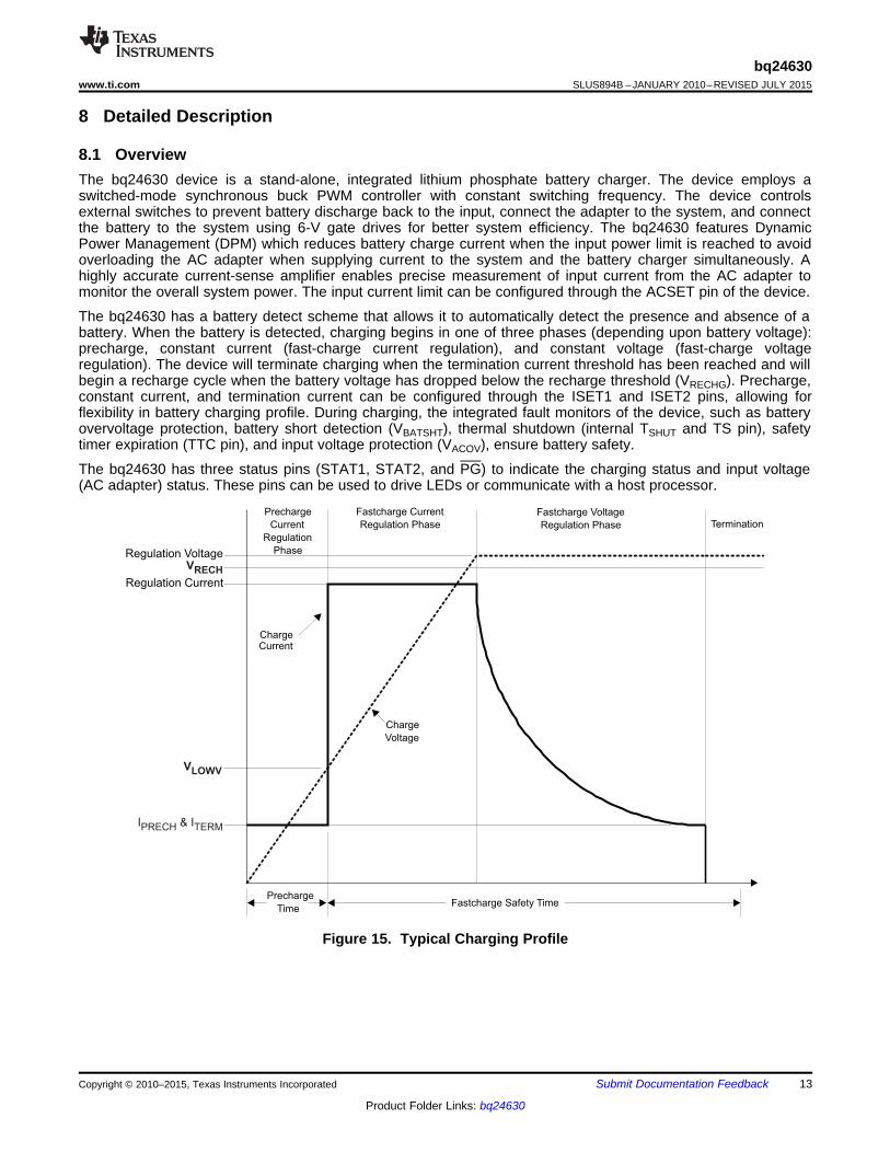
8 Detailed Description
8.1 OverviewThe bq24630 device is a stand-alone, integrated lithium phosphate battery charger. The device employs aswitched-mode synchronous buck PWM controller with constant switching frequency. The device controlsexternal switches to prevent battery discharge back to the input, connect the adapter to the system, and connectthe battery to the system using 6-V gate drives for better system efficiency. The bq24630 features DynamicPower Management (DPM) which reduces battery charge current when the input power limit is reached to avoidoverloading the AC adapter when supplying current to the system and the battery charger simultaneously. Ahighly accurate current-sense amplifier enables precise measurement of input current from the AC adapter tomonitor the overall system power. The input current limit can be configured through the ACSET pin of the device.
The bq24630 has a battery detect scheme that allows it to automatically detect the presence and absence of abattery. When the battery is detected, charging begins in one of three phases (depending upon battery voltage):precharge, constant current (fast-charge current regulation), and constant voltage (fast-charge voltageregulation). The device will terminate charging when the termination current threshold has been reached and willbegin a recharge cycle when the battery voltage has dropped below the recharge threshold (VRECHG). Precharge,constant current, and termination current can be configured through the ISET1 and ISET2 pins, allowing forflexibility in battery charging profile. During charging, the integrated fault monitors of the device, such as batteryovervoltage protection, battery short detection (VBATSHT), thermal shutdown (internal TSHUT and TS pin), safetytimer expiration (TTC pin), and input voltage protection (VACOV), ensure battery safety.
The bq24630 has three status pins (STAT1, STAT2, and PG) to indicate the charging status and input voltage(AC adapter) status. These pins can be used to drive LEDs or communicate with a host processor.
Figure 15. Typical Charging Profile
Copyright © 2010–2015, Texas Instruments Incorporated Submit Documentation Feedback 13
Product Folder Links: bq24630

VCC
ACDRV
BATDRV
BTST
HIDRV
PH
REGN
LODRV
GND
TS
bq24630
CE
ACP
ACN
VFB
SRP
6 V LDO
V(ACP-ACN)+
-
V(SRP-SRN)
COMPERROR
AMPLIFIER
1V
1.8 V
IBAT_ REG
SRN
VCC
VCC- 6 VREG
STATEMACHINE
LOGIC
BATTERYDETECTION
LOGIC
VCC
PH
4.2V
+_BTST REFRESH
SYSTEMPOWER
SELECTORLOGIC
CE
145 °C
IC Tj TSHUT
SRN+100 mV
VCC SLEEP
LEVELSHIFTER
ACN
+
-
+
-
+
-
+
-
+
-
+
-
V(SRP-SRN)CHG_OCP
+
-
160% X IBAT_REG
SYNCHSRP- SRN
ISET1
ISET2
ACSET
IBAT_ REGISET1
ISET18
5mV20X
BAT BAT_OVP
+
-
108% X VBAT_REGLTF
+
-
HTF
VREF
TCO +
-
+
-
SUSPEND
VCC ACOV+
-
VACOV
VREF
STAT1
STAT1
20X
STAT2
STAT2
3.3 VLDO
VCC
VFBLOWV
+
-
RCHRG
+-0.35V
+-1.675V
VFB
RCHRG
TERM
+
-
ISET2TERM
TERMINATE CHARGE
+
-
bq24630
+
-
+
-UVLO
VUVLO
VCCSLEEP
UVLO
VCC- 6 V
VCC- 6 V
ACN- 6 V
VCC- 6 VREG
ACN
ACN-6 V
ACOV
PWMCONTROL
LOGIC
+
-
PWM
+
-
+
-+-
PG
PG
+-
CHARGE
20mA
DISCHARGE
DISCHARGEOR
CHARGE
8 mA
BAT_OVP
+
-DISABLETMR/TERM
0.4 V
TTC
VOLTAGEREFERENCE
VREF
ACN- SRN
SRN+200 mV
+
-
ACN
Safety Timer
30 minutePrecharge
timer
TTC
FAULT
2 mA
FAULT
1 M
TTC
+
-
+
-
WARM
COOL
COOL
WARM
20mA
CE
1.25 mV
100X V(SRP -SRN)
bq24630SLUS894B –JANUARY 2010–REVISED JULY 2015 www.ti.com
8.2 Functional Block Diagram
14 Submit Documentation Feedback Copyright © 2010–2015, Texas Instruments Incorporated
Product Folder Links: bq24630
ISET2TERM
SR
VI =
100 R´
ACSETDPM
AC
VI =
20 R´
ISET1CHARGE
SR
VI =
20 R´
BAT
R2V = 1.8 V 1
R1
é ù´ +ê ú
ë û
bq24630www.ti.com SLUS894B –JANUARY 2010–REVISED JULY 2015
8.3 Feature Description
8.3.1 Battery Voltage RegulationThe bq24630 uses a high-accuracy voltage band gap and regulator for the high-accuracy charging voltage. Thecharge voltage is programmed via a resistor divider from the battery to ground, with the midpoint tied to the VFBpin. The voltage at the VFB pin is regulated to 1.8 V, giving Equation 1 for the regulation voltage:
(1)
Where R2 is connected from VFB to the battery and R1 is connected from VFB to GND.
8.3.2 Battery Current RegulationThe ISET1 input sets the maximum fast-charge current. Battery charge current is sensed by resistor RSRconnected between SRP and SRN. The full-scale differential voltage between SRP and SRN is 100 mV. Thus,for a 10-mΩ sense resistor, the maximum charging current is 10 A. Equation 2 is for charge current:
(2)
VISET1, the input voltage range of ISET1, is between 0 and 2 V. The SRP and SRN pins are used to sensevoltage across RSR with default value of 10 mΩ. However, resistors of other values can also be used. A largersense resistor gives a larger sense voltage and a higher regulation accuracy, but at the expense of higherconduction loss.
8.3.3 PrechargeOn powerup, if the battery voltage is below the VLOWV threshold, the bq24630 applies 125 mA precharge currentto the battery (1). The precharge feature is intended to revive deeply discharged cells. If the VLOWV threshold isnot reached within 30 minutes of initiating precharge, the charger turns off and a FAULT is indicated on thestatus pins.
8.3.4 Input Adapter Current RegulationThe total input from an ac adapter or other dc source is a function of the system supply current and the batterycharging current. System current normally fluctuates as portions of the system are powered up or down. Withoutdynamic power management (DPM), the source must be able to supply the maximum system current and themaximum charger input current simultaneously. By using DPM, the input current regulator reduces the chargingcurrent when the input current exceeds the input current limit set by ACSET. The current capability of the acadaptor can be lowered, reducing system cost.
Similar to setting battery regulation current, adaptor current is sensed by resistor RAC connected between ACPand ACN. Its maximum value is set by ACSET using Equation 3:
(3)
VACSET, the input voltage range of ACSET is between 0 and 2 V. The ACP and ACN pins are used to sensevoltage across RAC with a default value of 10 mΩ. However, resistors of other values can also be used. A largerthe sense resistor gives a larger sense voltage and a higher regulation accuracy, but at the expense of higherconduction loss.
8.3.5 Charge Termination, Recharge, and Safety TimerThe bq24630 monitors the charging current during the voltage regulation phase. When VTTC is valid, terminationis detected while the voltage on the VFB pin is higher than the VRECH threshold AND the charge current is lessthan the ITERM threshold, as calculated in Equation 4:
(4)
(1) Assuming a 10-mΩ sense resistor. 1.25 mV is regulated across SRP-SRN, regardless of the value of the sense resistor.
Copyright © 2010–2015, Texas Instruments Incorporated Submit Documentation Feedback 15
Product Folder Links: bq24630

CHARGE TTC TTCt = C K´
bq24630SLUS894B –JANUARY 2010–REVISED JULY 2015 www.ti.com
Feature Description (continued)VISET2, the input voltage of ISET2 is between 0 and 2 V. The minimum termination current is clamped to bearound 125 mA with a default 10-mΩ sensing resistor. To avoid early termination during WARM/COOL condition,set ITERM ≤ ICHARGE/10. As a safety backup, the bq24630 also provides a programmable charge timer. The chargetime is programmed by the capacitor connected between the TTC pin and GND, and is given by Equation 5:
(5)
Where CTTC (range from 0.047 µF to 0.47 µF to give 1-h to 10-h safety timer) is the capacitor connected fromTTC pin to GND, and KTTC is the constant multiplier (1.4 min/nF).
A new charge cycle is initiated and the safety timer is reset when one of the following conditions occurs:• The battery voltage falls below the recharge threshold.• A power-on-reset (POR) event occurs.• CE is toggled.
The TTC pin may be taken LOW to disable termination and to disable the safety timer. If TTC is pulled to VREF,the bq24630 continues to allow termination but disables the safety timer. TTC taken low resets the safety timer.When ACOV, VCCLOWV, and SLEEP mode resume normal, the safety timer is reset.
8.3.6 Power UpThe bq24630 uses a SLEEP comparator to determine the source of power on the VCC pin, because VCC can besupplied either from the battery or the adapter. If the VCC voltage is greater than the SRN voltage, the bq24630enables ACFET and disables BATFET. If all other conditions are met for charging, the bq24630 then attempts tocharge the battery (see Enable and Disable Charging section). If the SRN voltage is greater than VCC, indicatingthat the battery is the power source, the bq24630 enables the BATFET and enters a low-quiescent-current (<15-μA) SLEEP mode to minimize current drain from the battery.
If VCC is below the UVLO threshold, the device is disabled, ACFET turns off ,and BATFET turns on.
8.3.7 Enable and Disable ChargingThe following conditions must be valid before charge is enabled:• CE is HIGH.• The device is not in undervoltage lockout (UVLO) and not in VCCLOWV mode.• The device is not in SLEEP mode.• The VCC voltage is lower than the ac overvoltage threshold (VCC < VACOV).• 30-ms delay is complete after initial power up.• The REGN LDO and VREF LDO voltages are at the correct levels.• Thermal shut (TSHUT) is not valid.• TS fault is not detected.
Any of the following conditions stops ongoing charging:• CE is LOW.• Adapter is removed, causing the device to enter UVLO, VCCLOWV, or SLEEP mode.• Adapter is over voltage.• The REGN or VREF LDOs are overloaded.• TSHUT IC temperature threshold is reached (145°C on rising edge with 15°C hysteresis).• TS voltage goes out of range, indicating the battery temperature is too hot or too cold.• TTC saftey timer times out.
8.3.8 System Power SelectorThe bq24630 automatically switches adapter or battery power to the system load. The battery is connected to thesystem by default during power up or during SLEEP mode. The battery is disconnected from the system andthen the adapter is connected to the system 30 ms after exiting SLEEP. Automatic break-before-make logicprevents shoot-through currents when the selectors switch.
16 Submit Documentation Feedback Copyright © 2010–2015, Texas Instruments Incorporated
Product Folder Links: bq24630
o
o o
1f =
2 L Cp
bq24630www.ti.com SLUS894B –JANUARY 2010–REVISED JULY 2015
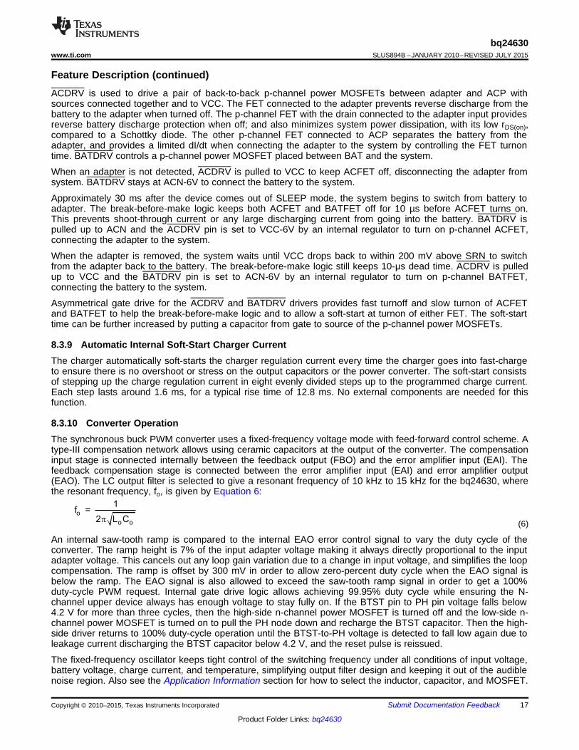
Feature Description (continued)ACDRV is used to drive a pair of back-to-back p-channel power MOSFETs between adapter and ACP withsources connected together and to VCC. The FET connected to the adapter prevents reverse discharge from thebattery to the adapter when turned off. The p-channel FET with the drain connected to the adapter input providesreverse battery discharge protection when off; and also minimizes system power dissipation, with its low rDS(on),compared to a Schottky diode. The other p-channel FET connected to ACP separates the battery from theadapter, and provides a limited dI/dt when connecting the adapter to the system by controlling the FET turnontime. BATDRV controls a p-channel power MOSFET placed between BAT and the system.
When an adapter is not detected, ACDRV is pulled to VCC to keep ACFET off, disconnecting the adapter fromsystem. BATDRV stays at ACN-6V to connect the battery to the system.
Approximately 30 ms after the device comes out of SLEEP mode, the system begins to switch from battery toadapter. The break-before-make logic keeps both ACFET and BATFET off for 10 µs before ACFET turns on.This prevents shoot-through current or any large discharging current from going into the battery. BATDRV ispulled up to ACN and the ACDRV pin is set to VCC-6V by an internal regulator to turn on p-channel ACFET,connecting the adapter to the system.
When the adapter is removed, the system waits until VCC drops back to within 200 mV above SRN to switchfrom the adapter back to the battery. The break-before-make logic still keeps 10-μs dead time. ACDRV is pulledup to VCC and the BATDRV pin is set to ACN-6V by an internal regulator to turn on p-channel BATFET,connecting the battery to the system.
Asymmetrical gate drive for the ACDRV and BATDRV drivers provides fast turnoff and slow turnon of ACFETand BATFET to help the break-before-make logic and to allow a soft-start at turnon of either FET. The soft-starttime can be further increased by putting a capacitor from gate to source of the p-channel power MOSFETs.
8.3.9 Automatic Internal Soft-Start Charger CurrentThe charger automatically soft-starts the charger regulation current every time the charger goes into fast-chargeto ensure there is no overshoot or stress on the output capacitors or the power converter. The soft-start consistsof stepping up the charge regulation current in eight evenly divided steps up to the programmed charge current.Each step lasts around 1.6 ms, for a typical rise time of 12.8 ms. No external components are needed for thisfunction.
8.3.10 Converter OperationThe synchronous buck PWM converter uses a fixed-frequency voltage mode with feed-forward control scheme. Atype-III compensation network allows using ceramic capacitors at the output of the converter. The compensationinput stage is connected internally between the feedback output (FBO) and the error amplifier input (EAI). Thefeedback compensation stage is connected between the error amplifier input (EAI) and error amplifier output(EAO). The LC output filter is selected to give a resonant frequency of 10 kHz to 15 kHz for the bq24630, wherethe resonant frequency, fo, is given by Equation 6:
(6)
An internal saw-tooth ramp is compared to the internal EAO error control signal to vary the duty cycle of theconverter. The ramp height is 7% of the input adapter voltage making it always directly proportional to the inputadapter voltage. This cancels out any loop gain variation due to a change in input voltage, and simplifies the loopcompensation. The ramp is offset by 300 mV in order to allow zero-percent duty cycle when the EAO signal isbelow the ramp. The EAO signal is also allowed to exceed the saw-tooth ramp signal in order to get a 100%duty-cycle PWM request. Internal gate drive logic allows achieving 99.95% duty cycle while ensuring the N-channel upper device always has enough voltage to stay fully on. If the BTST pin to PH pin voltage falls below4.2 V for more than three cycles, then the high-side n-channel power MOSFET is turned off and the low-side n-channel power MOSFET is turned on to pull the PH node down and recharge the BTST capacitor. Then the high-side driver returns to 100% duty-cycle operation until the BTST-to-PH voltage is detected to fall low again due toleakage current discharging the BTST capacitor below 4.2 V, and the reset pulse is reissued.
The fixed-frequency oscillator keeps tight control of the switching frequency under all conditions of input voltage,battery voltage, charge current, and temperature, simplifying output filter design and keeping it out of the audiblenoise region. Also see the Application Information section for how to select the inductor, capacitor, and MOSFET.
Copyright © 2010–2015, Texas Instruments Incorporated Submit Documentation Feedback 17
Product Folder Links: bq24630
bq24630SLUS894B –JANUARY 2010–REVISED JULY 2015 www.ti.com
Feature Description (continued)8.3.11 Synchronous and Non-Synchronous OperationThe charger operates in synchronous mode when the SRP-SRN voltage is above 5 mV (0.5-A inductor currentfor a 10-mΩ sense resistor). During synchronous mode, the internal gate-drive logic ensures there is break-before-make complementary switching to prevent shoot-through currents. During the 30-ns dead time where bothFETs are off, the body diode of the low-side power MOSFET conducts the inductor current. Having the low-sideFET turn on keeps the power dissipation low, and allows safely charging at high currents. During synchronousmode, the inductor current is always flowing and the converter operates in continuous-conduction mode (CCM),creating a fixed two-pole system.
The charger operates in non-synchronous mode when the SRP-SRN voltage is below 5 mV (0.5-A inductorcurrent for a 10-mΩ sense resistor). The charger is forced into non-synchronous mode when battery voltage islower than 2 V or when the average SRP-SRN voltage is lower than 1.25 mV.
During non-synchronous operation, the body-diode of the low-side MOSFET can conduct the positive inductorcurrent after the high-side n-channel power MOSFET turns off. When the load current decreases and theinductor current drops to zero, the body diode is be naturally turned off and the inductor current becomesdiscontinuous. This mode is called discontinuous-conduction mode (DCM). During DCM, the low-side n-channelpower MOSFET turns on for around 80 ns when the bootstrap capacitor voltage drops below 4.2 V; then the low-side power MOSFET turns off and stays off until the beginning of the next cycle, where the high-side powerMOSFET is turned on again. The 80-ns low-side MOSFET on-time is required to ensure the bootstrap capacitoris always recharged and able to keep the high-side power MOSFET on during the next cycle. This is importantfor battery chargers, where unlike regular dc-dc converters, there is a battery load that maintains a voltage andcan both source and sink current. The 80-ns low-side pulse pulls the PH node (connection between high- andlow-side MOSFETs) down, allowing the bootstrap capacitor to recharge up to the REGN LDO value. After 80 ns,the low-side MOSFET is kept off to prevent negative inductor current from occurring.
At very low currents during non-synchronous operation, there may be a small amount of negative inductorcurrent during the 80-ns recharge pulse. The charge should be low enough to be absorbed by the inputcapacitance. Whenever the converter goes into zero-percent duty cycle, the high-side MOSFET does not turn on,and the low-side MOSFET does not turn on (only 80-ns recharge pulse) either, and there is almost no dischargefrom the battery.
During the DCM mode, the loop response automatically changes and has a single-pole system at which the poleis proportional to the load current, because the converter does not sink current, and only the load provides acurrent sink. This means at very low currents the loop response is slower, as there is less sinking currentavailable to discharge the output voltage.
8.3.12 Cycle-By-Cycle Charge Undercurrent ProtectionIf the SRP-SRN voltage decreases below 5 mV (the charger is also forced into non-synchronous mode when theaverage SRP-SRN voltage is lower than 1.25 mV), the low-side FET is turned off for the remainder of theswitching cycle to prevent negative inductor current. During DCM, the low-side FET only turns on for at around80 ns when the bootstrap capacitor voltage drops below 4.2 V to provide refresh charge for the bootstrapcapacitor. This is important to prevent negative inductor current from causing a boost effect in which the inputvoltage increases as power is transferred from the battery to the input capacitors and leads to an overvoltagestress on the VCC node and potentially causes damage to the system.
8.3.13 Input Overvoltage Protection (ACOV)ACOV provides protection to prevent system damage due to high input voltage. Once the adapter voltagereaches the ACOV threshold, charge is disabled and the battery is switched to the system instead of the adapter.
8.3.14 Input Undervoltage Lockout (UVLO)The system must have a minimum VCC voltage to allow proper operation. This VCC voltage could come fromeither the input adapter or the battery, because a conduction path exists from the battery to VCC through thehigh-side NMOS body diode. When VCC is below the UVLO threshold, all circuits on the IC are disabled, and thegate drive bias to ACFET and BATFET is disabled.
18 Submit Documentation Feedback Copyright © 2010–2015, Texas Instruments Incorporated
Product Folder Links: bq24630
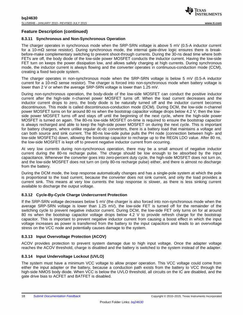
CHARGE SUSPENDED CHARGE SUSPENDED
TEMPERATURE RANGE TOINITIATE CHARGE
TEMPERATURE RANGEDURING A CHARGE CYCLE
VHTF
GND
VTCO
GND
VREF VREF
CHARGE SUSPENDED CHARGE SUSPENDED
VLTF VLTF
CHARGE at I /8CHARGE CHARGE at I /8CHARGE
VWARM
CHARGE at I /8CHARGE CHARGE at I /8CHARGE
VCOOL
CHARGE at ICHARGE CHARGE at ICHARGE
VCOOL
VWARM
VLTF_HYS
VCOOL_HYS
VWARM_HYS
bq24630www.ti.com SLUS894B –JANUARY 2010–REVISED JULY 2015
Feature Description (continued)8.3.15 Battery Overvoltage ProtectionThe converter does not allow the high-side FET to turn on until the BAT voltage goes below 105% of theregulation voltage. This allows one-cycle response to an overvoltage condition, such as occurs when the load isremoved or the battery is disconnected. An 8-mA current sink from SRP to GND is on only during charge andallows discharging the stored output inductor energy that is transferred to the output capacitors. BATOVP alsosuspends the safety timer.
8.3.16 Cycle-By-Cycle Charge Overcurrent ProtectionThe charger has a secondary cycle-to-cycle overcurrent protection. It monitors the charge current, and preventsthe current from exceeding 160% of the programmed charge current. The high-side gate drive turns off when theovercurrent is detected, and automatically resumes when the current falls below the overcurrent threshold.
8.3.17 Thermal Shutdown ProtectionThe QFN package has low thermal impedance, which provides good thermal conduction from the silicon to theambient, to keep junctions temperatures low. As an added level of protection, the charger converter turns off andself-protects whenever the junction temperature exceeds the TSHUT threshold of 145°C. The charger stays offuntil the junction temperature falls below 130°C. Then the charger soft-starts again if all other enable-chargeconditions are valid. Thermal shutdown also suspends the safety timer.
8.3.18 Temperature QualificationThe controller continuously monitors battery temperature by measuring the voltage between the TS pin andGND. A negative-temperature-coefficient thermistor (NTC) and an external voltage divider typically develop thisvoltage. The controller compares this voltage against its internal thresholds to determine if charging is allowed.To initiate a charge cycle, the battery temperature must be within the VLTF to VHTF thresholds. If batterytemperature is outside of this range, the controller suspends charge and the safety timer, and waits until thebattery temperature is within the VLTF to VHTF range. During the charge cycle, the battery temperature must bewithin the VLTF to VTCO thresholds. If the battery temperature is outside of this range, the controller suspendscharge and the safety timer, and waits until the battery temperature is within the VLTF to VHTF range. If the batterytemperature is between the VLTF and VCOOL thresholds or between the VHTF and VWARM thresholds, charge isautomatically reduced to ICHARGE/8. To avoid early termination during a COOL/WARM condition, set ITERM ≤ICHARGE/10. The controller suspends charge by turning off the PWM charge FETs. Figure 16 and Figure 17summarize the operation.
Figure 16. TS, Thermistor Sense ThresholdsCopyright © 2010–2015, Texas Instruments Incorporated Submit Documentation Feedback 19
Product Folder Links: bq24630

VREF
TS
RT2
RT1
RTH
103 AT
bq24630
VREF
COOL
COOL
V1
VRT1 =
1 1+
RT2 RTH
-
VREF COOL WARM
COOL WARM
VREF VREFWARM COOL
WARM COOL
1 1V RTH RTH
V VRT2 =
V VRTH 1 RTH 1
V V
æ ö´ ´ ´ -ç ÷
è ø
æ öæ ö´ - - ´ -ç ÷ç ÷
è ø è ø
Temperature
ProgrammedCharge Current
1/8 x ProgrammedCharge Current
ChargeCurrent
ChargeSuspended
ICH
AR
GE
G/8
Ch
arg
e
Charge at ICHG
I/8
CH
AR
GE
Ch
arg
e
ChargeSuspended
VLTF VCOOLVWARM
VHTF/VTCO
(I )CHARGE
(I /8)CHARGE
bq24630SLUS894B –JANUARY 2010–REVISED JULY 2015 www.ti.com
Feature Description (continued)
Figure 17. Typical Charge Current vs Temperature Profile
Assuming a 103AT NTC thermistor on the battery pack as shown in the Figure 22, the value RT1 and RT2 canbe determined by using Equation 7 and Equation 8:
(7)
(8)
Figure 18. TS Resistor Network
20 Submit Documentation Feedback Copyright © 2010–2015, Texas Instruments Incorporated
Product Folder Links: bq24630
bq24630www.ti.com SLUS894B –JANUARY 2010–REVISED JULY 2015
Feature Description (continued)For example, a 103AT NTC thermistor is used to monitor the battery pack temperature. Select TCOOL = 0ºC,TWARM = 60ºC. From the calculation and select standard 5% resistor value, RT1 = 2.2 kΩ, RT2 = 6.8 kΩ, andTCOLD is –17ºC (target –20ºC); THOT is 77ºC (target 75ºC), and TCUT-OFF is 86ºC (target 80ºC). A small RC filter issuggested to protect the TS pin from system-level ESD.
8.3.19 Timer Fault RecoveryThe bq24630 provides a recovery method to deal with timer fault conditions. The following summarizes thismethod:
Condition 1: The battery voltage is above the recharge threshold and a time-out fault occurs.
Recovery Method: The timer fault clears when the battery voltage falls below the recharge threshold, andbattery detection begins. Taking CE low, or a POR condition, also clears the fault.
Condition 2: The battery voltage is below the RECHARGE threshold and a time-out fault occurs.
Recovery Method: Under this scenario, the bq24630 applies the IFAULT current to the battery. This smallcurrent is used to detect a battery removal condition and remains on as long as the battery voltage stays belowthe recharge threshold. If the battery voltage goes above the recharge threshold, the bq24630 disables the faultcurrent and executes the recovery method described in Condition 1. Taking CE low, or a POR condition, alsoclears the fault.
8.3.20 PG OutputThe open drain PG (power-good) output indicates whether the VCC voltage is valid or not. The open-drain FETturns on whenever bq24630 has a valid VCC input (not in UVLO or ACOV or SLEEP mode). The PG pin can beused to drive an LED or communicate with the host processor.
8.3.21 CE (Charge Enable)The CE digital input is used to disable or enable the charge process. A high-level signal on this pin enablescharge, provided all the other conditions for charge are met (see Enable and Disable Charging). A high-to-lowtransition on this pin also resets all timers and fault conditions. There is an internal 1-MΩ pulldown resistor on theCE pin, so if CE is floated the charge does not turn on.
8.3.22 Charge Status OutputsThe open-drain STAT1 and STAT2 outputs indicate various charger operations as shown in Table 2. Thesestatus pins can be used to drive LEDs or communicate with the host processor. Note that OFF indicates that theopen-drain transistor is turned off.
Table 2. Stat Pin Definition for bq24630CHARGE STATE STAT1 STAT2
Charge in progress ON OFFCharge complete OFF ONCharge suspend, timer fault, overvoltage, sleep mode, battery absent OFF OFF
Copyright © 2010–2015, Texas Instruments Incorporated Submit Documentation Feedback 21
Product Folder Links: bq24630
POR or RECHARGE
Enable 125 mA Charge,
Start 0.5s timer
VFB > VRECH No
Battery Present,
Begin Charge
0.5s timer
expired
Yes
No
Yes
Disable 125 mA
Charge
Apply 8 mA discharge
current, start 1s timer
VFB < VLOWV No
Battery Present,
Begin Charge
1s timer
expired
Yes
No
Yes
Disable 8 mA
discharge current
The battery detection routine runs on
power up, or if VFB falls below VRECH
due to removing a battery or
discharging a battery
Battery Absent
bq24630SLUS894B –JANUARY 2010–REVISED JULY 2015 www.ti.com
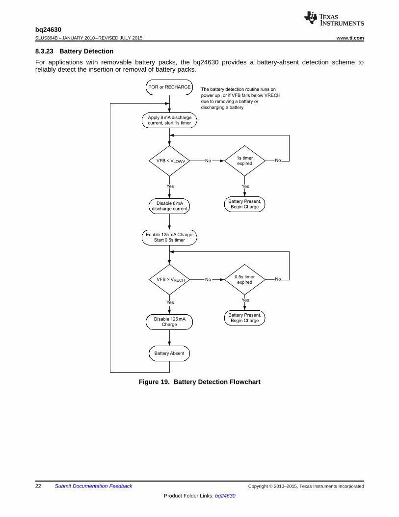
8.3.23 Battery DetectionFor applications with removable battery packs, the bq24630 provides a battery-absent detection scheme toreliably detect the insertion or removal of battery packs.
Figure 19. Battery Detection Flowchart
22 Submit Documentation Feedback Copyright © 2010–2015, Texas Instruments Incorporated
Product Folder Links: bq24630
´m
é ù´ ê úë û
MAX
8mA 1secC = = 930 F
500k1.425 1+
100k
´
é ù´ ê ú
ë û
DISCH DISCHMAX
2
1
I tC =
R1.425 1+
R
Battery
Inserted
Battery not Detected
Battery Detected
tLOWV_DEG tRECH_DEG
tWAKE
VREG
VRECH
VLOWV
(V )WAKE
(V )DISH
bq24630www.ti.com SLUS894B –JANUARY 2010–REVISED JULY 2015
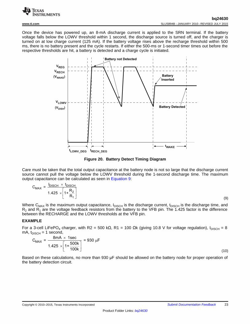
Once the device has powered up, an 8-mA discharge current is applied to the SRN terminal. If the batteryvoltage falls below the LOWV threshold within 1 second, the discharge source is turned off, and the charger isturned on at low charge current (125 mA). If the battery voltage rises above the recharge threshold within 500ms, there is no battery present and the cycle restarts. If either the 500-ms or 1-second timer times out before therespective thresholds are hit, a battery is detected and a charge cycle is initiated.
Figure 20. Battery Detect Timing Diagram
Care must be taken that the total output capacitance at the battery node is not so large that the discharge currentsource cannot pull the voltage below the LOWV threshold during the 1-second discharge time. The maximumoutput capacitance can be calculated as seen in Equation 9:
(9)
Where CMAX is the maximum output capacitance, IDISCH is the discharge current, tDISCH is the discharge time, andR2 and R1 are the voltage feedback resistors from the battery to the VFB pin. The 1.425 factor is the differencebetween the RECHARGE and the LOWV thresholds at the VFB pin.
EXAMPLEFor a 3-cell LiFePO4 charger, with R2 = 500 kΩ, R1 = 100 Ωk (giving 10.8 V for voltage regulation), IDISCH = 8mA, tDISCH = 1 second,
(10)
Based on these calculations, no more than 930 μF should be allowed on the battery node for proper operation ofthe battery detection circuit.
Copyright © 2010–2015, Texas Instruments Incorporated Submit Documentation Feedback 23
Product Folder Links: bq24630

bq24630SLUS894B –JANUARY 2010–REVISED JULY 2015 www.ti.com
8.4 Device Functional Modes
Figure 21. Device Operational Flow Chart
24 Submit Documentation Feedback Copyright © 2010–2015, Texas Instruments Incorporated
Product Folder Links: bq24630

RAC0.010 W
Q1 (ACFET)
N
P
ACN
ACP
ISET2
ACSET
VREF
CE
VFB
TS
VCC
HIDRV
N
PH
BTST
REGN
LODRV
GND
SRP
SRN
P
PACK+
PACK-
SYSTEMADAPTER+
ADAPTER-
C4
0.1 µF
C2 0.1 µFC3 C7
Q4
Q5
C6
L1
D1
BAT54
C5
C10
0.1 µF
TTC
CTTC
VREF
STAT2
PackThermistor
Sense
BATDRVACDRV
bq24630
P
Q2 (ACFET)
Q3 (BATFET)VREF
ISET1
STAT1
VBAT
R92.2 kW
R10
6.8 kW
R1100kW
PG
ADAPTER +
Cff22 pF
0.1 µF
1 µF
C810 µF
1 µF
1 µF
RSR0.010 W
C11
0.1 µF
C12
10 µF*
C13
10 µF*
R2
500kW
R12 10 kW
R11 10 kW
R13 10 kW
R3100 kW
R432.4 kW
R5100 kW
R610 kW
R7100 kW
R822.1 kW
R14100 kW
C140.1 mF
R15100 kW
C15
0.1 µF
PwrPad0.11 Fμ
R16
100 W
C10.1 Fμ103AT
SI7617DN
SI7617DN
SIS412DN
SIS412DN
SI7617DN
C910 μF
R1710Ω
R202Ω
C162.2μF
R181 kΩ
R191 kΩ
8.2 µH*
D2
D3
D4
bq24630www.ti.com SLUS894B –JANUARY 2010–REVISED JULY 2015
9 Application and Implementation
NOTEInformation in the following applications sections is not part of the TI componentspecification, and TI does not warrant its accuracy or completeness. TI’s customers areresponsible for determining suitability of components for their purposes. Customers shouldvalidate and test their design implementation to confirm system functionality.
9.1 Application InformationThe bq24630 battery charger is ideal for high current charging (up to 10 A) and can charge battery packsconsisting of single cells or multiple cells in series. The bq24630EVM is a complete charge module for evaluatingthe bq24630. The application curves were taken using the bq24630EVM. Refer to the EVM user's guide(SLUU396) for EVM information.
9.2 Typical Application
NOTE: VIN = 19 V, BAT = 3-cell LiFePO4, Iadapter_limit = 4 A, Icharge= 3 A, Ipre-charge= 0.125 A, Iterm= 0.3 A, 2.5-h safety timer
Figure 22. Typical System Schematic
9.2.1 Design RequirementsFor this design example, use the parameters listed in Table 3 as the input parameters.
Table 3. Design ParametersDESIGN PARAMETER EXAMPLE VALUE
AC adapter voltage (VIN) 19 VAC adapter current limit 4 ABattery charge voltage (number of cells in series) 10.8 V (3 cells)Battery charge current (during constant current phase) 3 A
Copyright © 2010–2015, Texas Instruments Incorporated Submit Documentation Feedback 25
Product Folder Links: bq24630
æ öD = -ç ÷
ç ÷è ø
2
BATo BAT2
INs
V1V V
V8LCf
RIPPLECOUT RIPPLE
II = 0.29 I
2 3
» ´
´
CIN CHGI = I D (1 D)´ ´ -
INRIPPLE
S
V D (1 D)I =
f L
´ ´ -
´
SAT CHG RIPPLEI I + (1/2) I³
bq24630SLUS894B –JANUARY 2010–REVISED JULY 2015 www.ti.com
Table 3. Design Parameters (continued)DESIGN PARAMETER EXAMPLE VALUE
Precharge current 0.125 ATermination current 0.3 ASafety timer 2.5 hours
9.2.2 Detailed Design Procedure
9.2.2.1 Inductor SelectionThe bq24630 has 300-kHz switching frequency to allow the use of small inductor and capacitor values. Inductorsaturation current should be higher than the charging current (ICHARGE) plus half the ripple current (IRIPPLE):
(11)
The inductor ripple current depends on input voltage (VIN), duty cycle (D = VOUT/VIN), switching frequency (fs) andinductance (L):
(12)
The maximum inductor ripple current happens with D = 0.5. For example, the battery charging voltage range isfrom 2.8 V to 14.4 V for a 4-cell battery pack. For 20-V adapter voltage, 10-V battery voltage gives the maximuminductor ripple current.
Usually, inductor ripple is designed in the range of 20%–40% of maximum charging current as a trade-offbetween inductor size and efficiency for a practical design.
The bq24630 has cycle-by-cycle charge undercurrent protection (UCP) by monitoring the charge-current sensingresistor to prevent negative inductor current. The typical UCP threshold is 5 mV falling edge, corresponding to0.5-A falling edge for a 10-mΩ charge-current sensing resistor.
9.2.2.2 Input CapacitorInput capacitor should have enough ripple-current rating to absorb the input switching-ripple current. The worst-case RMS ripple current is half of the charging current when the duty cycle is 0.5. If the converter does notoperate at 50% duty cycle, then the worst-case capacitor rms current ICIN occurs where the duty cycle is closestto 50% and can be estimated by the following equation:
(13)
A low-ESR ceramic capacitor such as X7R or X5R is preferred for the input decoupling capacitor and should beplaced as close as possible to the drain of the high-side MOSFET and source of the low-side MOSFET. Thevoltage rating of the capacitor must be higher than the normal input voltage level. A 25-V rating or highercapacitor is preferred for 20-V input voltage. A 20-µF capacitance is suggested for typical of 3-A to 4-A chargingcurrent.
9.2.2.3 Output CapacitorOutput capacitor also should have enough ripple current rating to absorb output switching ripple current. Theoutput capacitor RMS current ICOUT is given:
(14)
The output capacitor voltage ripple can be calculated as follows:
(15)
At certain input/output voltage and switching frequency, the voltage ripple can be reduced by increasing theoutput filter LC.
26 Submit Documentation Feedback Copyright © 2010–2015, Texas Instruments Incorporated
Product Folder Links: bq24630
2bottom CHG DS(on)P = (1 D) I R- ´ ´
REGN plt plton off
on off
V V VI = , I =
R R
-
SW GD GS
1Q = Q + Q
2´
SW SWon off
on off
Q Qt = , t =
I I
( )2top CHG DS(on) IN CHG on off S
1P = D I R + V I t + t f
2´ ´ ´ ´ ´ ´
top DS(on) GD bottom DS(on) GFOM = R Q FOM = R Q´ ´
bq24630www.ti.com SLUS894B –JANUARY 2010–REVISED JULY 2015
The bq24630 has internal loop compensator. To get good loop stability, the resonant frequency of the outputinductor and output capacitor should be designed between 10 kHz and 15 kHz. The preferred ceramic capacitoris 25 V, X7R or X5R for 4-cell applications.
9.2.2.4 Power MOSFET SelectionTwo external N-channel MOSFETs are used for a synchronous switching battery charger. The gate drivers areinternally integrated into the IC with 6 V of gate drive voltage. 30-V or higher voltage rating MOSFETs arepreferred for a 20-V input voltage and 40-V MOSFETs are prefered for 20-V to 28-V input voltage.
Figure of merit (FOM) is usually used for selecting the proper MOSFET based on a tradeoff between theconduction loss and switching loss. For a top-side MOSFET, FOM is defined as the product of a MOSFET on-resistance, rDS(on), and the gate-to-drain charge, QGD. For a bottom-side MOSFET, FOM is defined as the productof the MOSFET on-resistance, rDS(on), and the total gate charge, QG.
(16)
The lower the FOM value, the lower the total power loss. Usually, lower rDS(on) has higher cost with the samepackage size.
The top-side MOSFET loss includes conduction loss and switching loss. It is a function of duty cycle (D =VOUT/VIN), charging current (ICHARGE), MOSFET on-resistance (rDS(on)), input voltage (VIN), switching frequency(fS), turnon time (ton) and turnoff time (toff):
(17)
The first item represents the conduction loss. Usually, MOSFET rDS(on) increases by 50% with a 100ºC junctiontemperature rise. The second term represents the switching loss. The MOSFET turnon and turnoff times aregiven by:
(18)
where Qsw is the switching charge, Ion is the turnon gate-driving current, and Ioff is the turnoff gate-driving current.If the switching charge is not given in the MOSFET datasheet, it can be estimated by gate-to-drain charge (QGD)and gate-to-source charge (QGS):
(19)
Total gate-driving current can be estimated by the REGN voltage (VREGN), MOSFET plateau voltage (Vplt), totalturnon gate resistance (Ron), and turnoff gate resistance (Roff) of the gate driver:
(20)
The conduction loss of the bottom-side MOSFET is calculated with the following equation when it operates insynchronous continuous conduction mode:
(21)
If the SRP-SRN voltage decreases below 5 mV (the charger is also forced into non-synchronous mode when theaverage SRP-SRN voltage is lower than 1.25 mV), the low-side FET is turned off for the remainder of theswitching cycle to prevent negative inductor current.
As a result, all the freewheeling current goes through the body diode of the bottom-side MOSFET. The maximumcharging current in non-synchronous mode can be up to 0.9 A (0.5 A typ.) for a 10-mΩ charging-current sensingresistor, considering IC tolerance. Choose the bottom-side MOSFET with either an internal Schottky or bodydiode capable of carrying the maximum non-synchronous mode charging current.
MOSFET gate driver power loss contributes to the dominant losses on the controller IC when the buck converteris switching. Choosing a MOSFET with a small Qg_total reduces the IC power loss to avoid thermal shutdown.
Copyright © 2010–2015, Texas Instruments Incorporated Submit Documentation Feedback 27
Product Folder Links: bq24630
o
o o
1f =
2 L Cp
R12 W
C12.2 mF
D1
C20.1-1 mF
R24.7-30WAdapter
connectorVCC pin
(2010)(1206)
VREF IN VREF VREF
ICLOSS ICLOSS _ driver VREF Quiescent
P (V V ) I
P P P P
= - ×
= + +
ICLoss_driver IN g_total sP V Q f= × ×
bq24630SLUS894B –JANUARY 2010–REVISED JULY 2015 www.ti.com
(22)
where Qg_total is the total gate charge for both upper and lower MOSFET at 6-V VREGN.
The VREF load current is another component of the VCC input current (Do not overload VREF.), where total ICloss can be described by following equations:
(23)
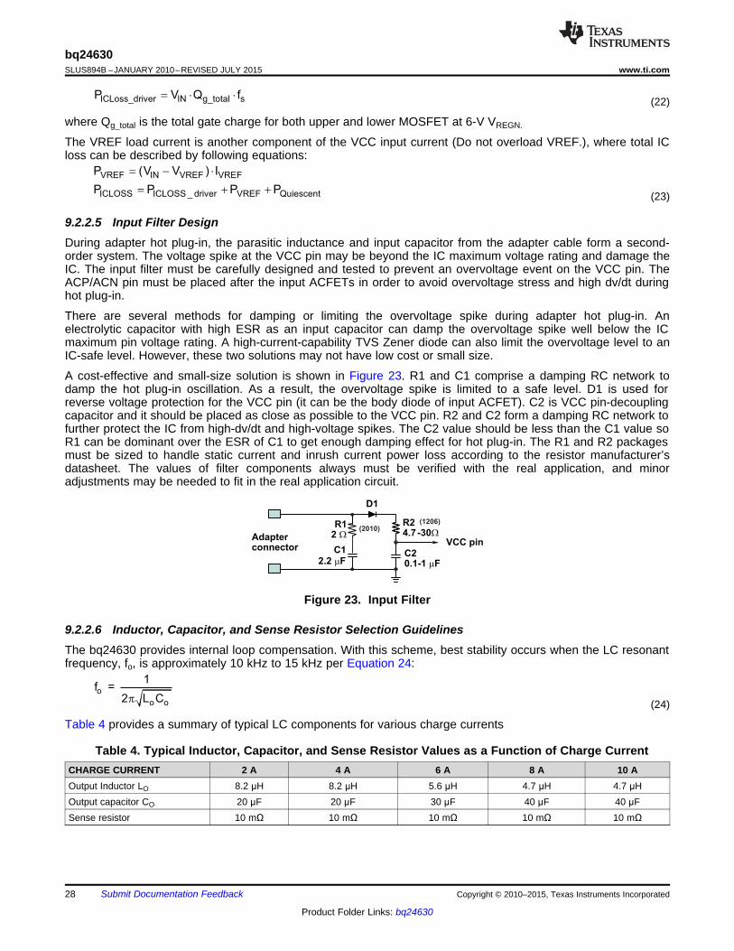
9.2.2.5 Input Filter DesignDuring adapter hot plug-in, the parasitic inductance and input capacitor from the adapter cable form a second-order system. The voltage spike at the VCC pin may be beyond the IC maximum voltage rating and damage theIC. The input filter must be carefully designed and tested to prevent an overvoltage event on the VCC pin. TheACP/ACN pin must be placed after the input ACFETs in order to avoid overvoltage stress and high dv/dt duringhot plug-in.
There are several methods for damping or limiting the overvoltage spike during adapter hot plug-in. Anelectrolytic capacitor with high ESR as an input capacitor can damp the overvoltage spike well below the ICmaximum pin voltage rating. A high-current-capability TVS Zener diode can also limit the overvoltage level to anIC-safe level. However, these two solutions may not have low cost or small size.
A cost-effective and small-size solution is shown in Figure 23. R1 and C1 comprise a damping RC network todamp the hot plug-in oscillation. As a result, the overvoltage spike is limited to a safe level. D1 is used forreverse voltage protection for the VCC pin (it can be the body diode of input ACFET). C2 is VCC pin-decouplingcapacitor and it should be placed as close as possible to the VCC pin. R2 and C2 form a damping RC network tofurther protect the IC from high-dv/dt and high-voltage spikes. The C2 value should be less than the C1 value soR1 can be dominant over the ESR of C1 to get enough damping effect for hot plug-in. The R1 and R2 packagesmust be sized to handle static current and inrush current power loss according to the resistor manufacturer’sdatasheet. The values of filter components always must be verified with the real application, and minoradjustments may be needed to fit in the real application circuit.
Figure 23. Input Filter
9.2.2.6 Inductor, Capacitor, and Sense Resistor Selection GuidelinesThe bq24630 provides internal loop compensation. With this scheme, best stability occurs when the LC resonantfrequency, fo, is approximately 10 kHz to 15 kHz per Equation 24:
(24)
Table 4 provides a summary of typical LC components for various charge currents
Table 4. Typical Inductor, Capacitor, and Sense Resistor Values as a Function of Charge CurrentCHARGE CURRENT 2 A 4 A 6 A 8 A 10 AOutput Inductor LO 8.2 μH 8.2 μH 5.6 μH 4.7 μH 4.7 μHOutput capacitor CO 20 μF 20 μF 30 μF 40 μF 40 μFSense resistor 10 mΩ 10 mΩ 10 mΩ 10 mΩ 10 mΩ
28 Submit Documentation Feedback Copyright © 2010–2015, Texas Instruments Incorporated
Product Folder Links: bq24630
bq24630www.ti.com SLUS894B –JANUARY 2010–REVISED JULY 2015
9.2.2.7 Typical System Circuit Component ListThe following table lists the components for the typical system circuit in Figure 22.
PART DESIGNATOR QTY DESCRIPTIONQ1, Q2, Q3 3 P-channel MOSFET, –30 V, –35 A, PowerPAK 1212-8, Vishay-Siliconix, Si7617DNQ4, Q5 2 N-channel MOSFET, 30 V, 12 A, PowerPAK 1212-8, Vishay-Siliconix, Sis412DND1 1 Diode, dual Schottky, 30 V, 200 mA, SOT23, Fairchild, BAT54CD2, D3, D4 3 LED diode, green, 2.1 V, 20 mA, LTST-C190GKTRAC, RSR 2 Sense resistor, 10 mΩ, 2010, Vishay-Dale, WSL2010R0100FL1 1 Inductor, 6.8 µH, 5.5 A, Vishay-Dale IHLP2525CZC2, C10 2 Capacitor, ceramic, 0.1 µF, 50 V, 10%, X7RC7 1 Capacitor, ceramic, 1 µF, 50 V, 10%, X7RC8, C9, C12, C13 4 Capacitor, ceramic, 10 µF, 35 V, 20%, X7RC4, C5 2 Capacitor, ceramic, 1 µF, 25 V, 10%, X7RC1, C3, C6, C11 4 Capacitor, ceramic, 0.1 µF, 16 V, 10%, X7RC14, C15 (Optional) 2 Capacitor, ceramic, 0.1 µF, 50 V, 10%, X7RC16 1 Capacitor, ceramic, 2.2 µF, 35 V, 10%, X7RCff 1 Capacitor, ceramic, 22 pF, 25 V, 10%, X7RCTTC 1 Capacitor, ceramic, 0.11 µF, 25 V, 5%, X7RR1, R3, R5, R7 4 Resistor, chip, 100 kΩ, 1/16W, 0.5%R2 1 Resistor, Chip, 500 kΩ, 1/16W, 0.5%R4 1 Resistor, chip, 32.4 kΩ, 1/16W, 0.5%R6 1 Resistor, chip, 10 kΩ, 1/16W, 0.5%R8 1 Resistor, chip, 22.1 kΩ, 1/16W, 0.5%R9 1 Resistor, chip, 2.2 kΩ, 1/16W, 5%R10 1 Resistor, chip, 6.8 kΩ, 1/16W, 5%R11, R12, R13 3 Resistor, chip, 10 kΩ, 1/16W, 5%R14, R15 (optional) 2 Resistor, chip, 100 kΩ, 1/16W, 5%R16 1 Resistor, chip, 100 Ω, 1/16W, 5%R17 1 Resistor, chip, 10 Ω, 1/4W, 5%R18, R19 2 Resistor, chip, 1 kΩ, 1/16W, 5%R20 1 Resistor, chip, 2 Ω, 1W, 5%
9.2.3 Application Curves
VIN: 24 V VBAT: 16 V ICHG = 3 A VIN: 24 V VBAT: 16 V
Figure 24. Continuous Conduction Mode Switching Figure 25. Battery Charging Soft StartWaveform
Copyright © 2010–2015, Texas Instruments Incorporated Submit Documentation Feedback 29
Product Folder Links: bq24630

bq24630SLUS894B –JANUARY 2010–REVISED JULY 2015 www.ti.com
10 Power Supply RecommendationsFor proper operation of bq24630, VCC must be from 5 V to 28 V. To begin charging, VCC must be higher thanSRN by at least 500 mV (otherwise, the device will be in sleep mode). TI recommends an input voltage of atleast 1.5 V to 2 V higher than the battery voltage, taking into consideration the DC losses in the high-side FET(Rdson), inductor (DCR), and input sense resistor (between ACP and ACN), the body diode drop of RBFETbetween VCC and input power supply, and battery sense resistor (between SRP and SRN). Power limit for theinput supply must be greater than the maximum power required by either the system load or for battery charging(the greater of the two).
11 Layout
11.1 Layout GuidelinesThe switching node rise and fall times should be minimized for minimum switching loss. Proper layout of thecomponents to minimize the high-frequency current path loop (see Figure 26) is important to prevent electricaland magnetic field radiation and high-frequency resonance problems. Here is a PCB layout priority list for properlayout. Layout of the PCB according to this specific order is essential.1. Place the input capacitor as close as possible to switching the MOSFET supply and ground connections and
use the shortest possible copper trace connection. These parts should be placed on the same layer of PCBinstead of on different layers using vias to make this connection.
2. The IC should be placed close to the switching MOSFET gate terminals, keeping the gate-drive signal tracesshort for a clean MOSFET drive. The IC can be placed on the other side of the PCB from the switchingMOSFETs.
3. Place the inductor input terminal as close as possible to the switching MOSFET output terminal. Minimize thecopper area of this trace to lower electrical and magnetic field radiation, but make the trace wide enough tocarry the charging current. Do not use multiple layers in parallel for this connection. Minimize parasiticcapacitance from this area to any other trace or plane.
4. The charging-current sensing resistor should be placed right next to the inductor output. Route the senseleads connected across the sensing resistor back to the IC in the same layer, close to each other (minimizeloop area), and do not route the sense leads through a high-current path (see Figure 27 for Kelvinconnection for best current accuracy). Place a decoupling capacitor on these traces next to the IC.
5. Place the output capacitor next to the sensing resistor output and ground.6. Output capacitor ground connections must be tied to the same copper that connects to the input capacitor
ground before connecting to system ground.7. Route the analog ground separately from the power ground and use a single ground connection to tie the
charger power ground to the charger analog ground. Just beneath the IC, use the copper pour for analogground, but avoid power pins to reduce inductive and capacitive noise coupling. Connect the analog groundto GND. Connect the analog ground and power ground together using the power pad as the single groundconnection point. Or use a 0-Ω resistor to tie the analog ground to power ground (the thermal pad should tieto analog ground in this case). A star-connection under the tharmal pad is highly recommended.
8. It is critical that the exposed thermal pad on the backside of the IC package be soldered to the PCB ground.Ensure that there are sufficient thermal vias directly under the IC connecting to the ground plane on the otherlayers.
9. Decoupling capacitors should be placed next to the IC pins; make the trace connections as short as possible.10. All via sizes and numbers should be adequate for a given current path.
See the EVM design (SLUU396) for recommended component placement of trace and via locations.
For VQFN information, see SCBA017 and SLUA271.
30 Submit Documentation Feedback Copyright © 2010–2015, Texas Instruments Incorporated
Product Folder Links: bq24630

Current Direction
To SRP - SRN pin or ACP - ACN pin
RSNS
Current Sensing Direction
High
Frequency
Current
Path
L1 R1
C3C1
C2PGND
SW VBAT
BATVIN
bq24630www.ti.com SLUS894B –JANUARY 2010–REVISED JULY 2015
11.2 Layout Example
Figure 26. High Frequency Current Path
Figure 27. Sensing Resistor PCB Layout
Copyright © 2010–2015, Texas Instruments Incorporated Submit Documentation Feedback 31
Product Folder Links: bq24630

bq24630SLUS894B –JANUARY 2010–REVISED JULY 2015 www.ti.com
12 Device and Documentation Support
12.1 Device Support
12.1.1 Third-Party Products DisclaimerTI'S PUBLICATION OF INFORMATION REGARDING THIRD-PARTY PRODUCTS OR SERVICES DOES NOTCONSTITUTE AN ENDORSEMENT REGARDING THE SUITABILITY OF SUCH PRODUCTS OR SERVICESOR A WARRANTY, REPRESENTATION OR ENDORSEMENT OF SUCH PRODUCTS OR SERVICES, EITHERALONE OR IN COMBINATION WITH ANY TI PRODUCT OR SERVICE.
12.2 Documentation Support
12.2.1 Related Documentationbq2461x/bq2463x EVM (HPA422) Multi-Cell Synchronous Switch-Mode Charger EVM User's Guide(SLUU396)Quad Flatpack No-Lead Logic Packages Application Report (SCBA017)QFN/SON PCB Attachment Application Report (SLUA271)
12.3 Community ResourcesThe following links connect to TI community resources. Linked contents are provided "AS IS" by the respectivecontributors. They do not constitute TI specifications and do not necessarily reflect TI's views; see TI's Terms ofUse.
TI E2E™ Online Community TI's Engineer-to-Engineer (E2E) Community. Created to foster collaborationamong engineers. At e2e.ti.com, you can ask questions, share knowledge, explore ideas and helpsolve problems with fellow engineers.
Design Support TI's Design Support Quickly find helpful E2E forums along with design support tools andcontact information for technical support.
12.4 TrademarksE2E is a trademark of Texas Instruments.All other trademarks are the property of their respective owners.
12.5 Electrostatic Discharge CautionThese devices have limited built-in ESD protection. The leads should be shorted together or the device placed in conductive foamduring storage or handling to prevent electrostatic damage to the MOS gates.
12.6 GlossarySLYZ022 — TI Glossary.
This glossary lists and explains terms, acronyms, and definitions.
13 Mechanical, Packaging, and Orderable InformationThe following pages include mechanical, packaging, and orderable information. This information is the mostcurrent data available for the designated devices. This data is subject to change without notice and revision ofthis document. For browser-based versions of this data sheet, refer to the left-hand navigation.
32 Submit Documentation Feedback Copyright © 2010–2015, Texas Instruments Incorporated
Product Folder Links: bq24630

PACKAGE OPTION ADDENDUM
www.ti.com 7-Apr-2015
Addendum-Page 1
PACKAGING INFORMATION
Orderable Device Status(1)
Package Type PackageDrawing
Pins PackageQty
Eco Plan(2)
Lead/Ball Finish(6)
MSL Peak Temp(3)
Op Temp (°C) Device Marking(4/5)
Samples
BQ24630RGER ACTIVE VQFN RGE 24 3000 Green (RoHS& no Sb/Br)
CU NIPDAU Level-2-260C-1 YEAR -40 to 85 OAT
BQ24630RGET ACTIVE VQFN RGE 24 250 Green (RoHS& no Sb/Br)
CU NIPDAU Level-2-260C-1 YEAR -40 to 85 OAT
(1) The marketing status values are defined as follows:ACTIVE: Product device recommended for new designs.LIFEBUY: TI has announced that the device will be discontinued, and a lifetime-buy period is in effect.NRND: Not recommended for new designs. Device is in production to support existing customers, but TI does not recommend using this part in a new design.PREVIEW: Device has been announced but is not in production. Samples may or may not be available.OBSOLETE: TI has discontinued the production of the device.
(2) Eco Plan - The planned eco-friendly classification: Pb-Free (RoHS), Pb-Free (RoHS Exempt), or Green (RoHS & no Sb/Br) - please check http://www.ti.com/productcontent for the latest availabilityinformation and additional product content details.TBD: The Pb-Free/Green conversion plan has not been defined.Pb-Free (RoHS): TI's terms "Lead-Free" or "Pb-Free" mean semiconductor products that are compatible with the current RoHS requirements for all 6 substances, including the requirement thatlead not exceed 0.1% by weight in homogeneous materials. Where designed to be soldered at high temperatures, TI Pb-Free products are suitable for use in specified lead-free processes.Pb-Free (RoHS Exempt): This component has a RoHS exemption for either 1) lead-based flip-chip solder bumps used between the die and package, or 2) lead-based die adhesive used betweenthe die and leadframe. The component is otherwise considered Pb-Free (RoHS compatible) as defined above.Green (RoHS & no Sb/Br): TI defines "Green" to mean Pb-Free (RoHS compatible), and free of Bromine (Br) and Antimony (Sb) based flame retardants (Br or Sb do not exceed 0.1% by weightin homogeneous material)
(3) MSL, Peak Temp. - The Moisture Sensitivity Level rating according to the JEDEC industry standard classifications, and peak solder temperature.
(4) There may be additional marking, which relates to the logo, the lot trace code information, or the environmental category on the device.
(5) Multiple Device Markings will be inside parentheses. Only one Device Marking contained in parentheses and separated by a "~" will appear on a device. If a line is indented then it is a continuationof the previous line and the two combined represent the entire Device Marking for that device.
(6) Lead/Ball Finish - Orderable Devices may have multiple material finish options. Finish options are separated by a vertical ruled line. Lead/Ball Finish values may wrap to two lines if the finishvalue exceeds the maximum column width.
Important Information and Disclaimer:The information provided on this page represents TI's knowledge and belief as of the date that it is provided. TI bases its knowledge and belief on informationprovided by third parties, and makes no representation or warranty as to the accuracy of such information. Efforts are underway to better integrate information from third parties. TI has taken andcontinues to take reasonable steps to provide representative and accurate information but may not have conducted destructive testing or chemical analysis on incoming materials and chemicals.TI and TI suppliers consider certain information to be proprietary, and thus CAS numbers and other limited information may not be available for release.
PACKAGE OPTION ADDENDUM
www.ti.com 7-Apr-2015
Addendum-Page 2
In no event shall TI's liability arising out of such information exceed the total purchase price of the TI part(s) at issue in this document sold by TI to Customer on an annual basis.

TAPE AND REEL INFORMATION
*All dimensions are nominal
Device PackageType
PackageDrawing
Pins SPQ ReelDiameter
(mm)
ReelWidth
W1 (mm)
A0(mm)
B0(mm)
K0(mm)
P1(mm)
W(mm)
Pin1Quadrant
BQ24630RGER VQFN RGE 24 3000 330.0 12.4 4.25 4.25 1.15 8.0 12.0 Q2
BQ24630RGER VQFN RGE 24 3000 330.0 12.4 4.25 4.25 1.15 8.0 12.0 Q2
BQ24630RGET VQFN RGE 24 250 180.0 12.4 4.25 4.25 1.15 8.0 12.0 Q2
BQ24630RGET VQFN RGE 24 250 180.0 12.4 4.25 4.25 1.15 8.0 12.0 Q2
PACKAGE MATERIALS INFORMATION
www.ti.com 7-Apr-2015
Pack Materials-Page 1
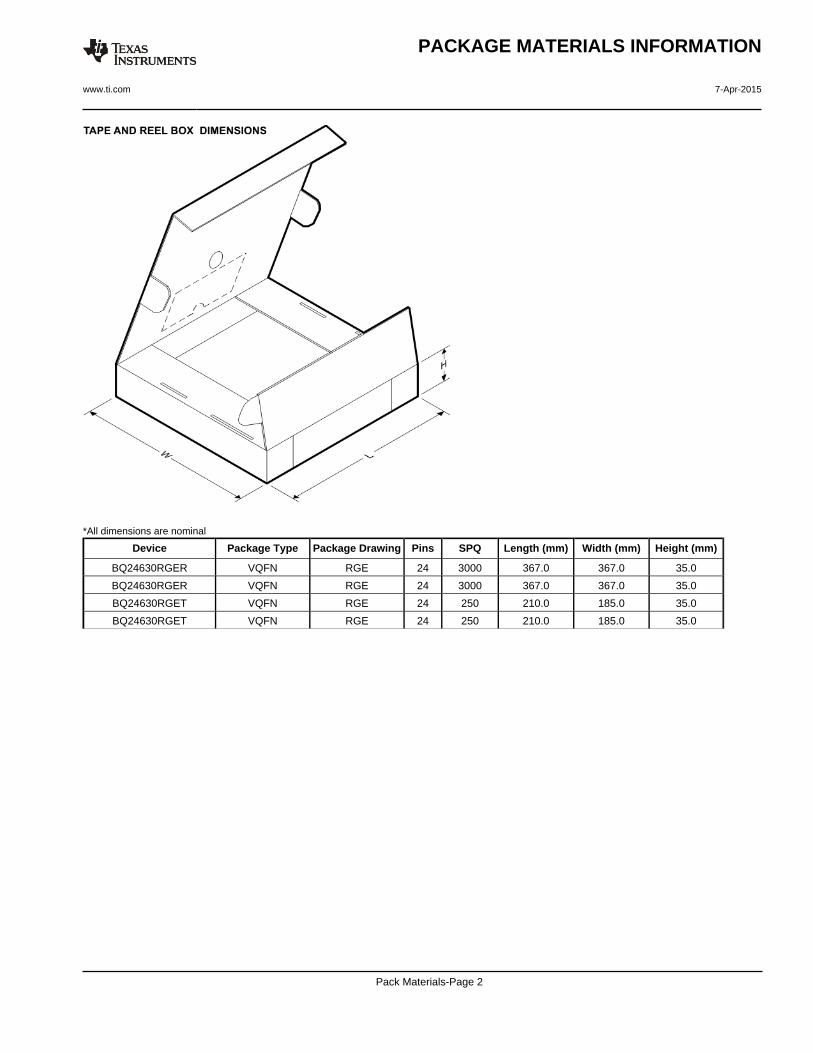
*All dimensions are nominal
Device Package Type Package Drawing Pins SPQ Length (mm) Width (mm) Height (mm)
BQ24630RGER VQFN RGE 24 3000 367.0 367.0 35.0
BQ24630RGER VQFN RGE 24 3000 367.0 367.0 35.0
BQ24630RGET VQFN RGE 24 250 210.0 185.0 35.0
BQ24630RGET VQFN RGE 24 250 210.0 185.0 35.0
PACKAGE MATERIALS INFORMATION
www.ti.com 7-Apr-2015
Pack Materials-Page 2

GENERIC PACKAGE VIEW
Images above are just a representation of the package family, actual package may vary.Refer to the product data sheet for package details.
RGE 24 VQFN - 1 mm max heightPLASTIC QUAD FLATPACK - NO LEAD
4204104/H

www.ti.com
PACKAGE OUTLINE
C
SEE TERMINALDETAIL
24X 0.30.2
2.45 0.1
24X 0.50.3
1 MAX
(0.2) TYP
0.050.00
20X 0.5
2X2.5
2X 2.5
A 4.13.9
B
4.13.9
0.30.2
0.50.3
VQFN - 1 mm max heightRGE0024BPLASTIC QUAD FLATPACK - NO LEAD
4219013/A 05/2017
PIN 1 INDEX AREA
0.08 C
SEATING PLANE
1
6 13
18
7 12
24 19
(OPTIONAL)PIN 1 ID
0.1 C A B0.05
EXPOSEDTHERMAL PAD
25 SYMM
SYMM
NOTES: 1. All linear dimensions are in millimeters. Any dimensions in parenthesis are for reference only. Dimensioning and tolerancing per ASME Y14.5M. 2. This drawing is subject to change without notice. 3. The package thermal pad must be soldered to the printed circuit board for thermal and mechanical performance.
SCALE 3.000
DETAILOPTIONAL TERMINAL
TYPICAL
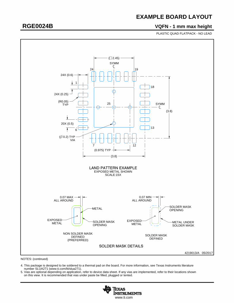
www.ti.com
EXAMPLE BOARD LAYOUT
0.07 MINALL AROUND
0.07 MAXALL AROUND
24X (0.25)
24X (0.6)
( 0.2) TYPVIA
20X (0.5)
(3.8)
(3.8)
( 2.45)
(R0.05)TYP
(0.975) TYP
VQFN - 1 mm max heightRGE0024BPLASTIC QUAD FLATPACK - NO LEAD
4219013/A 05/2017
SYMM
1
6
7 12
13
18
1924
SYMM
LAND PATTERN EXAMPLEEXPOSED METAL SHOWN
SCALE:15X
NOTES: (continued) 4. This package is designed to be soldered to a thermal pad on the board. For more information, see Texas Instruments literature number SLUA271 (www.ti.com/lit/slua271).5. Vias are optional depending on application, refer to device data sheet. If any vias are implemented, refer to their locations shown on this view. It is recommended that vias under paste be filled, plugged or tented.
25
SOLDER MASKOPENING
METAL UNDERSOLDER MASK
SOLDER MASKDEFINED
EXPOSEDMETAL
METAL
SOLDER MASKOPENING
SOLDER MASK DETAILS
NON SOLDER MASKDEFINED
(PREFERRED)
EXPOSEDMETAL

www.ti.com
EXAMPLE STENCIL DESIGN
24X (0.6)
24X (0.25)
20X (0.5)
(3.8)
(3.8)
4X ( 1.08)
(0.64)TYP
(0.64) TYP
(R0.05) TYP
VQFN - 1 mm max heightRGE0024BPLASTIC QUAD FLATPACK - NO LEAD
4219013/A 05/2017
NOTES: (continued) 6. Laser cutting apertures with trapezoidal walls and rounded corners may offer better paste release. IPC-7525 may have alternate design recommendations.
25
SYMM
METALTYP
SOLDER PASTE EXAMPLEBASED ON 0.125 mm THICK STENCIL
EXPOSED PAD 25
78% PRINTED SOLDER COVERAGE BY AREA UNDER PACKAGESCALE:20X
SYMM
1
6
7 12
13
18
1924

IMPORTANT NOTICE
Texas Instruments Incorporated (TI) reserves the right to make corrections, enhancements, improvements and other changes to itssemiconductor products and services per JESD46, latest issue, and to discontinue any product or service per JESD48, latest issue. Buyersshould obtain the latest relevant information before placing orders and should verify that such information is current and complete.TI’s published terms of sale for semiconductor products (http://www.ti.com/sc/docs/stdterms.htm) apply to the sale of packaged integratedcircuit products that TI has qualified and released to market. Additional terms may apply to the use or sale of other types of TI products andservices.Reproduction of significant portions of TI information in TI data sheets is permissible only if reproduction is without alteration and isaccompanied by all associated warranties, conditions, limitations, and notices. TI is not responsible or liable for such reproduceddocumentation. Information of third parties may be subject to additional restrictions. Resale of TI products or services with statementsdifferent from or beyond the parameters stated by TI for that product or service voids all express and any implied warranties for theassociated TI product or service and is an unfair and deceptive business practice. TI is not responsible or liable for any such statements.Buyers and others who are developing systems that incorporate TI products (collectively, “Designers”) understand and agree that Designersremain responsible for using their independent analysis, evaluation and judgment in designing their applications and that Designers havefull and exclusive responsibility to assure the safety of Designers' applications and compliance of their applications (and of all TI productsused in or for Designers’ applications) with all applicable regulations, laws and other applicable requirements. Designer represents that, withrespect to their applications, Designer has all the necessary expertise to create and implement safeguards that (1) anticipate dangerousconsequences of failures, (2) monitor failures and their consequences, and (3) lessen the likelihood of failures that might cause harm andtake appropriate actions. Designer agrees that prior to using or distributing any applications that include TI products, Designer willthoroughly test such applications and the functionality of such TI products as used in such applications.TI’s provision of technical, application or other design advice, quality characterization, reliability data or other services or information,including, but not limited to, reference designs and materials relating to evaluation modules, (collectively, “TI Resources”) are intended toassist designers who are developing applications that incorporate TI products; by downloading, accessing or using TI Resources in anyway, Designer (individually or, if Designer is acting on behalf of a company, Designer’s company) agrees to use any particular TI Resourcesolely for this purpose and subject to the terms of this Notice.TI’s provision of TI Resources does not expand or otherwise alter TI’s applicable published warranties or warranty disclaimers for TIproducts, and no additional obligations or liabilities arise from TI providing such TI Resources. TI reserves the right to make corrections,enhancements, improvements and other changes to its TI Resources. TI has not conducted any testing other than that specificallydescribed in the published documentation for a particular TI Resource.Designer is authorized to use, copy and modify any individual TI Resource only in connection with the development of applications thatinclude the TI product(s) identified in such TI Resource. NO OTHER LICENSE, EXPRESS OR IMPLIED, BY ESTOPPEL OR OTHERWISETO ANY OTHER TI INTELLECTUAL PROPERTY RIGHT, AND NO LICENSE TO ANY TECHNOLOGY OR INTELLECTUAL PROPERTYRIGHT OF TI OR ANY THIRD PARTY IS GRANTED HEREIN, including but not limited to any patent right, copyright, mask work right, orother intellectual property right relating to any combination, machine, or process in which TI products or services are used. Informationregarding or referencing third-party products or services does not constitute a license to use such products or services, or a warranty orendorsement thereof. Use of TI Resources may require a license from a third party under the patents or other intellectual property of thethird party, or a license from TI under the patents or other intellectual property of TI.TI RESOURCES ARE PROVIDED “AS IS” AND WITH ALL FAULTS. TI DISCLAIMS ALL OTHER WARRANTIES ORREPRESENTATIONS, EXPRESS OR IMPLIED, REGARDING RESOURCES OR USE THEREOF, INCLUDING BUT NOT LIMITED TOACCURACY OR COMPLETENESS, TITLE, ANY EPIDEMIC FAILURE WARRANTY AND ANY IMPLIED WARRANTIES OFMERCHANTABILITY, FITNESS FOR A PARTICULAR PURPOSE, AND NON-INFRINGEMENT OF ANY THIRD PARTY INTELLECTUALPROPERTY RIGHTS. TI SHALL NOT BE LIABLE FOR AND SHALL NOT DEFEND OR INDEMNIFY DESIGNER AGAINST ANY CLAIM,INCLUDING BUT NOT LIMITED TO ANY INFRINGEMENT CLAIM THAT RELATES TO OR IS BASED ON ANY COMBINATION OFPRODUCTS EVEN IF DESCRIBED IN TI RESOURCES OR OTHERWISE. IN NO EVENT SHALL TI BE LIABLE FOR ANY ACTUAL,DIRECT, SPECIAL, COLLATERAL, INDIRECT, PUNITIVE, INCIDENTAL, CONSEQUENTIAL OR EXEMPLARY DAMAGES INCONNECTION WITH OR ARISING OUT OF TI RESOURCES OR USE THEREOF, AND REGARDLESS OF WHETHER TI HAS BEENADVISED OF THE POSSIBILITY OF SUCH DAMAGES.Unless TI has explicitly designated an individual product as meeting the requirements of a particular industry standard (e.g., ISO/TS 16949and ISO 26262), TI is not responsible for any failure to meet such industry standard requirements.Where TI specifically promotes products as facilitating functional safety or as compliant with industry functional safety standards, suchproducts are intended to help enable customers to design and create their own applications that meet applicable functional safety standardsand requirements. Using products in an application does not by itself establish any safety features in the application. Designers mustensure compliance with safety-related requirements and standards applicable to their applications. Designer may not use any TI products inlife-critical medical equipment unless authorized officers of the parties have executed a special contract specifically governing such use.Life-critical medical equipment is medical equipment where failure of such equipment would cause serious bodily injury or death (e.g., lifesupport, pacemakers, defibrillators, heart pumps, neurostimulators, and implantables). Such equipment includes, without limitation, allmedical devices identified by the U.S. Food and Drug Administration as Class III devices and equivalent classifications outside the U.S.TI may expressly designate certain products as completing a particular qualification (e.g., Q100, Military Grade, or Enhanced Product).Designers agree that it has the necessary expertise to select the product with the appropriate qualification designation for their applicationsand that proper product selection is at Designers’ own risk. Designers are solely responsible for compliance with all legal and regulatoryrequirements in connection with such selection.Designer will fully indemnify TI and its representatives against any damages, costs, losses, and/or liabilities arising out of Designer’s non-compliance with the terms and provisions of this Notice.
Mailing Address: Texas Instruments, Post Office Box 655303, Dallas, Texas 75265Copyright © 2018, Texas Instruments Incorporated