Embed Size (px)
Citation preview

OPEN ACCESS
Bound-to-continuum terahertz quantum cascadelaser with a single-quantum-well phononextraction/injection stageTo cite this article: Maria I Amanti et al 2009 New J. Phys. 11 125022
View the article online for updates and enhancements.
You may also likeDynamically protected cat-qubits: a newparadigm for universal quantumcomputationMazyar Mirrahimi, Zaki Leghtas, Victor VAlbert et al.
-
Getting around the cell: physical transportin the intracellular worldSaurabh S Mogre, Aidan I Brown andElena F Koslover
-
New frontiers in quantum cascade lasers:high performance room temperatureterahertz sourcesMikhail A Belkin and Federico Capasso
-
Recent citationsDeep learning control of THz QCLsBenedikt Limbacher et al
-
Bayesian optimization of quantumcascade detectorsJohannes Popp et al
-
Optical properties of a triple AlGaAs/GaAsquantum well purported for quantumcascade laser active regionM.K. Bahar et al
-
This content was downloaded from IP address 212.225.132.103 on 07/12/2021 at 15:34

T h e o p e n – a c c e s s j o u r n a l f o r p h y s i c s
New Journal of Physics
Bound-to-continuum terahertz quantum cascadelaser with a single-quantum-well phononextraction/injection stage
Maria I Amanti1, Giacomo Scalari1, Romain Terazzi1,Milan Fischer1, Mattias Beck1, Jérome Faist1,3, Alok Rudra2,Pascal Gallo2 and Eli Kapon2
1 Institute of Quantum Electronics, ETH Zurich, Switzerland2 Laboratory of Physics of Nanostructures, Ecole Polytechnique Federale deLausanne (EPFL), SwitzerlandE-mail: [email protected]
New Journal of Physics 11 (2009) 125022 (19pp)Received 24 July 2009Published 17 December 2009Online at http://www.njp.org/doi:10.1088/1367-2630/11/12/125022
Abstract. A terahertz quantum cascade laser design that combines a widegain bandwidth, large photon-driven transport and good high-temperaturecharacteristics is presented. It relies on a diagonal transition between abound state and doublet of states tunnel coupled to the upper state of aphonon extraction stage. The high optical efficiency of this design enables theobservation of photon-driven transport over a wide current density range. Therelative tolerance of the design to small variations in the barrier thicknesses madeit suitable for testing different growth techniques and materials. In particular,we compared the performances of devices grown using molecular-beam epitaxywith those achieved using organometallic chemical vapor deposition. The low-threshold current density and the high slope efficiency makes this device anattractive active region for the development of single-mode quantum cascadelasers based on third-order-distributed feedback structures. Single-mode, highpower was achieved with good continuous and pulsed wave operation.
3 Author to whom any correspondence should be addressed.
New Journal of Physics 11 (2009) 1250221367-2630/09/125022+19$30.00 © IOP Publishing Ltd and Deutsche Physikalische Gesellschaft

2
Contents
1. Introduction 22. Design and simulations 3
2.1. Population inversion: architectures . . . . . . . . . . . . . . . . . . . . . . . . 32.2. Energy states and dipoles . . . . . . . . . . . . . . . . . . . . . . . . . . . . . 62.3. Lifetimes . . . . . . . . . . . . . . . . . . . . . . . . . . . . . . . . . . . . . 6
3. Growth and processing 94. Light–current and voltage–current characteristics 10
4.1. Doping and growth dependence of the performances . . . . . . . . . . . . . . 104.2. Discussion of the transport characteristics . . . . . . . . . . . . . . . . . . . . 134.3. Temperature dependence of the performances . . . . . . . . . . . . . . . . . . 14
5. Magnetotransport 156. Distributed feedback QCL 167. Conclusion 17Acknowledgments 18References 18
1. Introduction
The terahertz frequency range, loosely defined as the spectrum between 1–10 THz, hastraditionally been lacking convenient optical sources. Terahertz radiation has some importantpotential applications [1, 2] in imaging, chemical sensing and telecommunications. The longwavelength of terahertz radiation enables good penetration into heavily diffusing materialssuch as foams or small-grained material. The vibrational modes of large organic and inorganicmolecules are in the terahertz region, offering potential avenues for label-free sensing ofDNA [3]. The terahertz range has also some very interesting radio-astronomical applications,as it houses, among other important spectral signatures, the brightest cooling lines of the denseinterstellar medium ([CII] 158 µm, [OI] 63 and 145 µm) present in space. Because of the lackof transparency of the atmosphere in the terahertz region, such observation must be performedfrom airborne or spaceborne telescopes such as SOPHIA [4], putting additional constraints onthe optical sources.
For this reason, there is a strong interest in the development of terahertz sources that aretunable, portable and manufacturable in quantities. Recently, much progress has been madein sources based on nonlinear generation from either ultrafast lasers or continuous wave near-infrared or even mid-infrared [5] sources. Compared with these techniques based on nonlinearmixing, fundamental oscillators have the potential advantage of offering higher efficiencies andan easier fabrication technology.
The operation of quantum cascade lasers [6] was first achieved in the terahertz in 2001at a frequency of 4.1 THz, in pulsed mode and up to a maximum operating temperature of65 K [7]. Continuous wave operation was achieved shortly thereafter [8], followed by operationabove liquid nitrogen temperatures [9]. The introduction of a design based on resonant opticalphonon extraction [10] combined with the use of metal–metal waveguides [11] has enabled asignificant increase in the maximum operating temperature achieved by these devices, up to
New Journal of Physics 11 (2009) 125022 (http://www.njp.org/)

3
a maximum temperature of 186 K [12]. Even if this last result is a significant improvementcompared with the first generation devices, it still lies significantly below the temperaturesachievable by thermoelectric cooler based on Peltier effects.
Another challenge was to explore to what extent the operating range of these devicescould be expanded beyond the first range of operation of 3–4 THz. On the low-frequency side,optimization of the design of a bound-to-continuum transition lead to operation at 2.3 THz [13]and subsequently at 1.9 THz [14]. The addition of an electron reservoir energetically decoupledfrom the miniband-enabled operation of these devices down to a frequency of 1.2 THz[15, 16].
So far, applications of terahertz quantum cascade lasers have been restricted to proof-of-principle applications, even though some very encouraging results have already beenachieved [17]. Real-time, stand-off imaging using a microbolometer camera has also beendemonstrated [18]. Imaging of biological material with potential relevance for therapy wasrecently reported [19]. The results closest to a final application have been demonstrated in radio-astronomy: quantum cascade lasers have been used as local oscillators, pumping a hot electronbolometer and demonstrating a competitive receiver noise temperature [20]. Another importantstep is the report, recently achieved [21], of phase-locking of a THz quantum cascade laser ontoa microwave reference.
For many of these applications, the challenge is to find a quantum design that offers at thesame time a good manufacturability, high wallplug efficiency, and a high maximum operatingtemperature. Usually, a broad gain bandwidth is an advantage as it allows devices at variouswavelengths to be fabricated from the same epilayer material.
In this paper, we want to evaluate a design based on a short bound-to-continuumtransition with a one-well injector operating around 3 THz. The design is described and studiedtheoretically in section 2. In section 3, a brief description of the growth and processing of thedevices grown either by molecular beam epitaxy (MBE) or by organometallic chemical vapordeposition (OMCVD) is presented. In section 4, we report the characterization of such devicesin operating temperature and slope efficiency. The results of magnetospectroscopy are reportedin section 5. In section 6, we report the results of third-order-distributed feedback quantumcascade lasers fabricated using this laser material.
2. Design and simulations
2.1. Population inversion: architectures
Gain between subbands depends critically on the population inversion. As noted very earlyin the context of mid-infrared quantum cascade lasers [22, 23] and using the notations shownschematically in figure 1, the population inversion is maximized by achieving the largest ratioof upper to lower lifetime τ32/τ2, a large injection efficiency in the upper state η, and a longupper state lifetime τ3. The standard approach used in mid-infrared quantum cascade lasers hasbeen to use the properties of the intersubband non-radiative transitions to achieve a large ratioof lifetimes, and to employ a resonant tunneling injection of the electrons from the injectorinto the upper state to obtain a high value of η. For terahertz quantum cascade lasers, a similarapproach has worked very well at cryogenic temperatures. The active region architecture ofthe first quantum cascade laser operating in the terahertz [7] is essentially a scaled versionof a mid-infrared chirped-superlattice active region [24], in which the population inversion
New Journal of Physics 11 (2009) 125022 (http://www.njp.org/)

4
3
21–η
ητ31τ32
τ2
hν3
2
∆
(a)
(b)
(c) 3
2hω
LO
3
2
hωLO
(d)
g
g
g
g
hν
hν
Figure 1. (a) Schematic levels of a generic quantum cascade laser. By tradition,the upper level is labeled 3. (b) Bound-to-continuum or superlattice design. (c)Design based on a resonant tunneling extraction on an optical phonon resonantstage, as demonstrated by the MIT group [10]. (d) Bound-to-continuum withoptical phonon resonant extraction stage.
between the two states at the edge of the miniband is obtained by a phase space argument.The scattering rate from the lower state τ−1
2 is very large, the latter being the upper state of thelower miniband while the scattering from the upper state is similarly spread among the wholelower miniband, keeping the scattering rate into the lower state small, i.e. τ−1
32 τ−12 . Similarly,
the bound-to-continuum approach reported in [9] is a transposed version of the same approachdemonstrated at shorter wavelengths [23, 25]. In the bound-to-continuum design, the populationinversion achieved by a combination of the phase space used in the superlattice active regionwith a diagonal transition between states with a reduced spatial overlap, further enhancingthe population inversion. The bound-to-continuum approach was further developed [13, 26]and yielded devices with a very high slope efficiency and power at temperatures of about20 K. However, the maximum operating temperature of these devices remained limited toabout 100 K. The problem originates from the scaling of the miniband width 1 with photon
New Journal of Physics 11 (2009) 125022 (http://www.njp.org/)

5
energy hν, considering the effect of temperature kT and the broadening of the individuallevels 0. For the miniband and bound-to-continuum approach to succeed, one should maintainthe miniband width much larger than the broadening of the individual levels 1 0 and largerthan the thermal energy 1 > kT . In the mid-infrared, at room temperature (kT = 26 meV)the conditions are satisfied because 1 = 100–150 meV 0 ≈ 5 − 10 meV and 1 > kT . Inthe terahertz, however, the same inequality only holds at cryogenic temperature because theminiband width is only 15 meV, while the broadening at room temperature remains of the orderof a few meV. Similarly, one cannot keep a very wide miniband 1 = 100 meV with a photonenergy of hν = 15 meV, as the latter should be much larger than the individual level spacingof the miniband. In addition, as soon as the sum of the miniband width and the photon energybecomes equal or larger than the optical phonon energy 1 + hν > hωLO = 36 meV, the lifetimeof the upper state drops very strongly even at low temperatures. As a result, no terahertz laserhas ever been demonstrated to operate in this regime. In fact, there are no combinations ofstates where population inversion has been demonstrated for temperatures significantly largerthan 100 K solely based on intersubband scattering.
As shown schematically in figure 1(c), coupling by resonant tunneling the lower state of thelaser transition to a very short-lived upper state of a nearby well allows a significant reductionof the lower state lifetime while preserving a long upper state lifetime. This idea is the basis ofthe so-called resonant phonon design first demonstrated by the MIT group [10]. This design hasseen many variations [27, 28] and the current version has demonstrated the highest operatingtemperature of a THz quantum cascade laser so far [12]. The low lifetime of the upper level ofthe well following the active region is usually achieved by spacing the levels resonantly withan optical phonon energy. In this way, the condition 1 > kT is satisfied. This architecture hasthe additional benefit of shifting the intersubband absorption of the electrons from the groundstate of the quantum well to a photon energy larger than the laser transition. The transfer ofsome or all of the oscillator strengths from the ground state from very low frequencies tofrequencies above the transition energy was one of the key ingredient for the achievement ofintersubband lasers between 1.2–2 THz [16]. In that case, the pair of states were spaced byless than the optical phonon energy. A general feature of these designs is the requirement fora simultaneous alignment of the injector and extraction stage at the same electric field [29].Such a double resonance condition, however, increases the sensitivity of the design to growthinaccuracies.
A third class of designs aims at combining the advantages of both approaches. As shownschematically in figure 1(d), the active stage is based on a bound-to-continuum transition, whilethe miniband is coupled to an extractor quantum well [30]. This architecture has the advantageof reducing the direct coupling between the upper state and the extractor well since they arephysically separated by the length of the miniband region. The alignment condition on theextraction stage is also somewhat relaxed by the fact that it has to be satisfied over the widthof the miniband and no longer over the one of a single state. The original design followingthis architecture [30] was based on a five-quantum-well active region and two-quantum-wellinjector region. In this paper, we report on the study of a shortened version of this design,where the total number of quantum wells has been reduced to four, with a three-quantum-wellactive region coupled to a one-quantum-well injector. The latter choice was made to increasethe maximum operating temperature of the device. A four-quantum-well structure with a singlewell injector was also reported in [31]; that structure had, however, a very different active regionwith a much larger oscillator strength.
New Journal of Physics 11 (2009) 125022 (http://www.njp.org/)

6
In a quantum cascade laser, in the limit of vanishing waveguide losses, the gain mustonly balance the losses of the active region itself. As a result, in a simplified model, it canbe shown [32] that a figure of merit for the active region can be expressed as a product of anormalized gain cross section g∗ and a normalized lifetime τ ∗, with
g∗= f ′ω2τ 2
‖, (1)
where f ′ is the normalized oscillator strength of the laser transition at angular frequencyω and τ‖ the lifetime associated with the intersubband broadening. The normalized lifetimeτ ∗ is given by
τ ∗=
τup
τtrans, (2)
where τup is the effective upper state lifetime and τtrans the transit time across the whole activeregion. In a simple model of transport, the transit time increases with the number of states ofthe active region that are thermally populated. The latest results in high-temperature operationof terahertz quantum cascade lasers agree with this consideration, as the highest operatingtemperatures are achieved with designs based on three quantum wells [5, 12] and a total offour levels including the upper state one. An additional benefit of these designs with a reducednumber of quantum wells is the fact that the transport can be driven by the photon field, as allother states apart from the upper one contribute very weakly to the transport time. Comparedwith designs with more quantum wells, these devices suffer however from inherently largeleakage currents.
2.2. Energy states and dipoles
A schematic band diagram of the structure is shown in figure 2. Shown also are the energiesand electron probability densities, computed in the extended basis spanning the whole periodlength. The key parameters of the design, computed using a self-consistent Schrödinger–Poissonsolver, are listed in table 1. The latter can either use population obtained assuming a uniformthermal distribution or the transport populations obtained from the solution of the density matrixproblem. However, because of the low doping, the correction to the potential remains smallregardless of the assumption on the electron distribution. The two distributions are comparedin figure 3 at a temperature of 150 K. For this reason, in the simulations we assumed, forsimplicity, a uniform electronic temperature 50 K above the lattice one. The oscillator strengthis concentrated mainly on the transition between levels five and four of the active region. Asshown in figure 2, the wavefunctions of these two states have a relatively weak spatial overlap,that translates into a reduced normalized oscillator strength f ′
= m∗ f = 0.31. As expected forsuch a diagonal transition, the scattering rate from optical phonons yields still a relatively longlifetime at elevated temperature (τ = 1.9 ps at 150 K).
2.3. Lifetimes
As shown in figure 2, the wavefunction of the lower state n = 4 spans the complete length ofthe active region of the structure. As a result, it is expected that the computed value of thelower state lifetime depends on the assumption on the coherence length of the electron. In thissituation, a description in a local basis [29], where the period is split between an active region(first three quantum wells) and the extractor well, is physically a more meaningful approach.
New Journal of Physics 11 (2009) 125022 (http://www.njp.org/)

7
Distance (Å)
Ene
rgy
(eV
)Injection barrier
5432
1
800 1000200 400 60000
0.20
0.25
0.15
0.10
0.05
Figure 2. Schematic conduction band diagram of one stage of the structureEV1116 under an applied electric field of 7.6 × 10³ V cm−2. The moduli squaredof the relevant wavefunctions are shown. The layer sequence of one period ofstructure, in nanometers, right to left and starting from the injection barrieris 5.5/11.0/1.8/11.5/3.8/9.4/4.2/18.4 where Al0.15Ga0.85As layers are in bold,GaAs in roman and underlined number correspond to doped layer with Si toNd = 2 × 1016 cm−3. The dashed boxes represent the position of the local basis.
Table 1. Key computed parameters of the structure. hω is the photon energy, zthe dipole matrix element, f the oscillator strength, f ′
= f ∗ m∗ the normalizedoscillator strength, i the coupling energy between the upper state and theinjector level of the previous period, e the coupling energy between the lowerstates and the upper state of the extractor well, FNDR the field at the anticrossingand τ150 the upper state lifetime at 150 K.
hω z f f ′ i e FNDR τ150
12 meV 44 Å 5.5 0.36 0.5 meV 1 meV 7.6 kV cm−1 1.9 ps
In fact, we focus on the lifetime values at elevated temperature, where the in-plane dephasingrate τ−1
‖is close to the coupling energy he between the lower state and the upper state of the
extractor quantum well. To measure the in-plane dephasing rate, the transmission of the activeregion at terahertz frequency was measured using an ultrafast laser source and the results fittedusing a Drude model [33]. Assuming this value, we compute a product eτ‖ = 0.76 at 150 K. Inthe local basis, the lower state lifetime can be written as (neglecting the second-order scattering
New Journal of Physics 11 (2009) 125022 (http://www.njp.org/)

8
0
0.5
1.0
1.5
2.0
2.5
3.0
0 0.02 0.04 0.06 0.08 0.1 0.12 0.14Energy (eV)
Popu
latio
n (c
m
)–2
Injectorground state
Upper laserstate
Simulation 150 K
Thermal modelTransport
Figure 3. The subband populations versus the energy accounted from thebottom of the conduction band (red). The transport populations computed fromthe density matrix problem (green). The electrons distributed thermally for atemperature of 150 K. As shown by the red curve the population inversion isalmost zero for this temperature.
terms [34] for simplicity):
τl =1 + 12
eτ2‖
22eτ‖
+ 2τe, (3)
where e is the coupling energy and 1e the detuning between the lower state and the upperstate of the extractor well with lifetime τe. The above relation well expresses the limitation ofthe scheme based on resonant tunneling extraction: even in the limit of very strong coupling(eτ‖ 1) the lower state lifetime τl cannot decrease below 2τe ≈ 1 ps. As a reference, thelifetime of the upper state of a square quantum well decreases from a value of 1.1 to 0.6 psbetween 200 and 300 K. These values stress the challenge of designing a THz quantum cascadelaser based on resonant tunneling extraction that would operate above 200 K. The computedvalue of the lifetimes for our structure and using the above approach is shown in figure 4(a). Thecomputation includes optical phonon, intersubband roughness and impurity scatterings [35].As expected, the upper and lower states lifetime cross at a temperature slightly above 230 K,defining a clear absolute maximum in the operation temperature to achieve population inversion.
Transport and gain have been computed using a theory based on density matrix theory [34].Electron temperature was assumed to be uniform in the whole device, and for simplicityassumed to be larger than the lattice one by 50 K; electron–electron scattering was, however,not explicitly introduced. The computed current–voltage characteristics, computed at a latticetemperature of 100 and 150 K, are reported in figure 4(b). The gain was also computed as
New Journal of Physics 11 (2009) 125022 (http://www.njp.org/)

9
8
6
4
2
0
Ele
ctri
c fi
eld
(kV
cm
–1)
300250200150100500Current density (A cm–2 )
100 K 150 K
200
150
100
50
0Peak
gai
n (c
m–1 )
86420Electric field (kV cm)
6
81
2
4
6
810
2
Lif
etim
e (p
s)
25020015010050Lattice temperature (K)
Upper state lifetime
Extraction time
(a) (b)
0
Figure 4. (a) Computed value of the upper τu and lower state lifetimes τl asa function of temperature. (b) Voltage–current characteristics, computed for atemperature of 100 and 150 K. Inset: computed gain as a function of injectedcurrent at the same temperatures.
Table 2. Structural characteristics of the samples studied in this work. dinj anddextr refer to the injection and extraction barrier thickness, respectively, ns is thesheet density per period and 1Lper
Lperthe deviation from the nominal thickness of
the grown layers.
Sample Growth dinj (Å) dextr (Å) Nper ns (cm−2)1Lper
Lper(%)
N907 MBE 55 48 160 1.1 × 10¹¹ +0.6EV1116 MBE 55 48 180 5.5 × 10¹⁰
−2.7EV1157 MBE 55 48 180 3.7 × 10¹⁰
−2.43025A OMCVD 48 39 158 7 × 10¹⁰ +53057A/B OMCVD 48 39 158 1.8 × 10¹¹ 0
a function of electric field strength for these two temperatures and plotted in the inset. Asshown in the following section, the general features of the 4, as well as the maximum operatingtemperature, are well reproduced experimentally.
3. Growth and processing
The samples were grown using either solid-source MBE or OMCVD on GaAs substrates usingstandard growth conditions described in more details in [36, 37]. The samples studied as well astheir main characteristics are listed in table 2. It was found that the properties of the OMCVDgrown samples were dependent on the misorientation of the substrate. The two OMCVDsamples (3057A,B) were grown in the same run on substrates with the same misorientation(2), but oriented towards different crystallographic directions (111) A or (111) B.Only the sample 3025A, misoriented towards (111) A was measured.
New Journal of Physics 11 (2009) 125022 (http://www.njp.org/)

10
(a) (b)
Frequency (THz)2.6 3.0 3.4Frequency (THz)
2.6 3.0 3.410 K
80 K
152 K
10 K
80 K
100 K
120 K
140 K
152 K(X10)
10 K80 K
150 K
10 K
80 K
100 K
120 K
140 K150 K(X10)
Current (A)0.2 0.4 0.6 0.8 1.0 1.2 1.4
Vol
tage
(V
)
0.00
4
8
12
0
1
2
3
Peak power (m
W)1
2
3
Current (A)0.2 0.4 0.6 0.8 1.0 1.2 1.40.0
01.6 1.8
0
4
10 4
Vol
tage
(V
)
Peak power (m
W)
2
6
8
Current (mA cm–2 )0 200 400 600 800 1000
Current (mA cm–2)400 500100 200 3000
Figure 5. Light and bias-voltage versus current characteristics in pulsed mode oftwo samples for various representative temperatures. The samples are 1 mm longand 150 µm wide. (a) N907, with a higher doping. (b) EV1116, with a lowerdoping. Insets: representative spectra of the devices operated in pulsed mode.
As much as possible, the samples were processed using similar steps. After a first Ti/Aumetalization, the sample is wafer bonded on a GaAs carrier substrate. The sample substrate isthen removed by selective etching, the etch stop layer removed and ridges are processed by wetor dry etching. After processing, the samples were cleaved, indium soldered and wire-bondedon copper submounts.
4. Light–current and voltage–current characteristics
The samples were mounted on the cold head of a He flow-cryostat. The light- and bias-versuscurrent characteristics were measured in pulsed mode as a function of the temperature. Allthe optical power measurements were carried out either in pulsed or continuous wave with aterahertz absolute power meter (Thomas Keating Ltd) without any intermediate optics due tothe large surface of the detector.
4.1. Doping and growth dependence of the performances
The light versus current characteristics of the MBE-grown sample N907, relatively heavilydoped, is reported as a function of temperature in figure 5(a). The maximum operationtemperature achieved in the device shown is 152 K. A lower doped version of the same layer,EV1116, shows very similar characteristics and reached a maximum operating temperatureof 150 K for the device shown in figure 5(b) and of 160 K for the best device. Bothsamples exhibited a fairly wide emission spectrum spanning between 2.8 and 3.2 THz. Thecharacterization of the samples reported in table 2 was performed in a similar way. The keyresults are reported in the table 3. The voltage–current and light-current of the two samplesgrown by OMCVD are reported in figure 6, along with an atomic force microscopy image of arepresentative surface. As shown by the comparison of the two images, both the amplitude ofthe roughness as well as its characteristic periodicity are very different. A statistical analysis of
New Journal of Physics 11 (2009) 125022 (http://www.njp.org/)

11
Table 3. Key experimental results for samples studied.
Sample ν (THz) Jth (10 K) JNDR (10 K) Tmax (K) Jmax (Tmax)
N907 3.1 390 A cm−2 810 A cm−2 152 920 A cm−2
EV1116 3.1 200 A cm−2 400 A cm−2 160 520 A cm−2
EV1157 3.1 175 A cm−2 225 A cm−2 140 430 A cm−2
3025A 2.65 360 A cm−2 580 A cm−2 140 700 A cm−2
3057A 3.0 600 A cm−2 900 A cm−2 150 1050 A cm−2
3057B 3.1 820 A cm−2 1420 A cm−2 150 1640 A cm−2
0 250 500 750 1000
0
250
500
750
1000
3057A 3057B
0
250
500
750
1000
0 250 500 750 10000
1
2
4
5
6nm
0.4
0.8
1.2
1.6
0
nm
nm
Current (A)
Current density (A cm–2)
Peak power (m
W)
Vol
tage
(V
)
Vol
tage
(V
)
0
2
4
3
1
512
8
4
0.0 0.5 1.0 1.5 2
0 200 400 600 800 1000 1200Current density (A cm–2)
Peak power (m
W)
0 400 800 1200 1600
0
0.4
1.2
0.8
Current (A) 0.0 1.0 2.0 3.0
12
8
00
nm
10 K
100 K145 K(X10)
10 K
100 K
150 K(X5)
10 K 150 K
10 K
145 K
4
Figure 6. Comparison of two devices grown in a single OMCVD run using twosubstrates with different misorientations, 2 either towards the (111)A (3057A,left panel) or the (111)B direction (3057B, right panel). As shown by theatomic force microscopy images (top), the surfaces have a different microscopicroughness. The sample misoriented towards the (111)B direction shows a widerdynamical range and a higher maximum operating temperature. We attributethe higher maximum and threshold current of the latter device to a higherincorporation of silicon impurities during growth.
the two atomic force microscopy (AFM) images shows a root-mean-square amplitude of theroughness of 1 nm, with a characteristic length of 500 nm for the sample misoriented towards(111)A whereas the amplitude drops to 280 pm over about 50 nm for the misorientation towards
New Journal of Physics 11 (2009) 125022 (http://www.njp.org/)

12
Cur
rent
den
sity
(A
cm
–2 )
0
500
1000
1500
2000
0 0.5 1.0 1.5 2.0Doping (1E11 cm–2)
Threshold current density at 10 K
Roll-over point at maximum temperature
Figure 7. Maximum current at the optical roll-over point at the maximumtemperature (squares) and threshold current density at 10 K (filled disks) versussheet carrier density of the active region ns for the samples specified in table 2.Sample 3057A was, however, omitted as it displayed lower performances than3057B. The slope of the curve yields the minimum transport time across a periodτtrans = 19 ps. The fact that the threshold current density extrapolates to zerofor vanishing doping is a strong indication that the threshold current density islimited by the voltage-current characteristics rather than by the active regionlosses.
(111)B. The higher operating temperature, as well as the wider dynamical range shown bythe sample with the misorientation directed towards (111)B is consistent with the smalleramplitude of the interface roughness, and the results originating from this sample are reportedin the table 3. We attribute the higher maximum current reached by the sample misorientedtowards (111)B to a stronger incorporation of the silicon impurities. The maximum currentat the onset of negative differential resistance at the maximum temperature (i.e. at 150 K), aswell as the threshold current at 10 K are reported in figure 7. According to these data, we notethat both the roll-over point at the maximum operating temperature and threshold currents are,in a good approximation, proportional to the active region doping. Such a result was alreadyobtained for the case of bound-to-continuum active region designs [38]. They indicate that theelectron–electron interactions remain weak up to the maximum doping of the samples studied.In addition, the performance of the devices with thinner injection and extraction barriers, aresimilar to the reference ones, showing that the transport is not limited by the tunneling rate inand out of the active region. The slope of the Jmax versus ns yields the average transport timeacross one period. The value found for this design is τtrans = 19 ps. As a result, in our structurethe value of the effective time τ ∗ drops to 0.1 at 150 K. As the upper state lifetime is fixedby optical phonon scattering, the challenge would be to find ways of further decreasing thetransport time to improve τ ∗. As expected, the diagonal three-quantum-well structure reportedrecently [12] exhibits a shorter value of the transit time, but at the cost of a larger leakagecurrent for the same doping. The fact that the threshold current density is found to be linear asa function of doping had been interpreted in two ways. In [38], it was argued that, in a similar
New Journal of Physics 11 (2009) 125022 (http://www.njp.org/)

13
50
100
150
0
200
400
No laserLaser
dI/d
V (
A V
cm
–2 )C
urre
nt d
ensi
ty (
A c
m–2 )
Voltage per period (V)
0 0.02 0.04 0.06 0.08
0 0.02 0.04 0.06 0.08
hν+hνLO
Vol
tage
(V
)
0
2
4
6
8
10
0
1
2
3
4
0 100 200 300 400 500 600
100 150 200 250 300 350 400
dV/d
I (Ω
)
0.00
0.02
0.04
0.06
Current density (A cm )–2
Current (A)
Peak power (m
W)
0 50(a) (b)
Figure 8. (a) Light, current and differential resistance characteristics versusapplied bias for the sample EV1116 measured in continuous wave. (b) Currentdensity (top panel) and differential conductance (bottom panel) as a function ofthe applied bias per period for a lasing and a non-lasing device.
way as what is occurring in mid-infrared quantum cascade lasers, the active region opticallosses are dominated by the tails of intersubband absorption from the electrons of the injector.As a result, the threshold current is expected to increase linearly with active region doping.However, in other studies of active regions based on resonant phonon extraction [39, 40],it was argued that the laser threshold is controlled by the voltage and not by the currentthrough the active region losses, and therefore the threshold current dependence in dopingis a simple result of the scaling of the current–voltage characteristics. The waveguide losseshave two different origins: on the one hand, there are the active region optical losses, that areexpected to grow linearly with doping; on the other hand, the losses originating from the metalcontacts are of course independent from doping. As a result, we expect the threshold currentdensity to extrapolate to a nonzero value, representing the contribution of the metal losses tothe threshold, for vanishing doping; whereas a zero value is expected for a threshold currentcontrolled by voltage. Inspection of these characteristics for our devices shows that, in contrastto the bound-to-continuum samples discussed in [38], we are in a situation where the thresholdcurrent is mostly controlled by the applied bias. As discussed later, we understand that thisvoltage-controlled behavior is a feature of designs with low number of active wells and morespecifically of devices with single-quantum-well injectors.
4.2. Discussion of the transport characteristics
The voltage, light and differential resistance versus current characteristics of device EV1116are shown in figure 8(a) in continuous wave operation. The maximum of differential resistanceappearing at 120 A cm−2 corresponds to the situation where the injector is aligned betweenthe lower and the upper states. After a decrease of the differential resistance accompanyingthe alignment of the injector with the upper state of the laser transition, laser threshold isreached at a current density of 175 A cm−2, accompanied by a very sharp change of slope ofthe current–voltage characteristics. The current in the laser device reaches 400 A cm−2 before
New Journal of Physics 11 (2009) 125022 (http://www.njp.org/)
14
Thr
esho
ld c
urre
nt d
ensi
ty (
A c
m–2 )
0
100
200
300
400
500
100 150500Lattice temperature (K)
EV1116
Experimental dataTheory
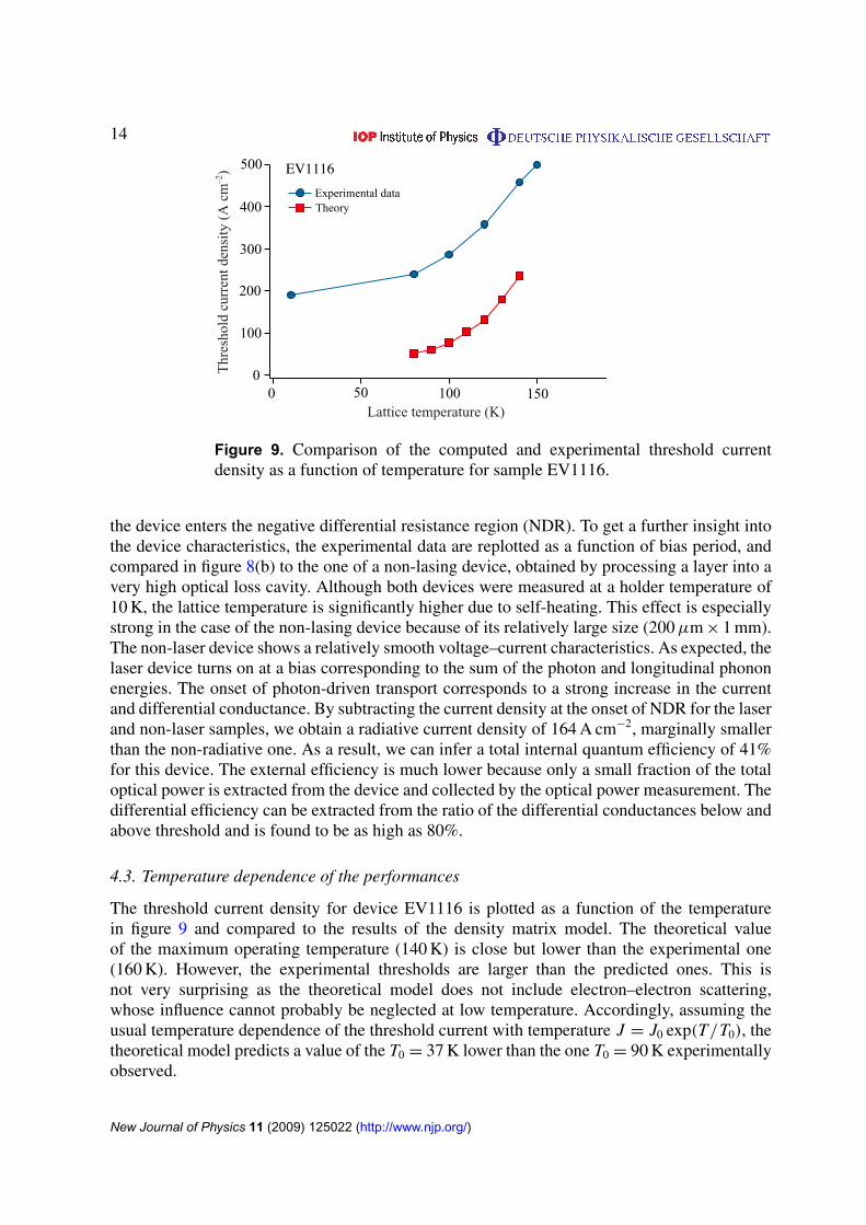
Figure 9. Comparison of the computed and experimental threshold currentdensity as a function of temperature for sample EV1116.
the device enters the negative differential resistance region (NDR). To get a further insight intothe device characteristics, the experimental data are replotted as a function of bias period, andcompared in figure 8(b) to the one of a non-lasing device, obtained by processing a layer into avery high optical loss cavity. Although both devices were measured at a holder temperature of10 K, the lattice temperature is significantly higher due to self-heating. This effect is especiallystrong in the case of the non-lasing device because of its relatively large size (200 µm × 1 mm).The non-laser device shows a relatively smooth voltage–current characteristics. As expected, thelaser device turns on at a bias corresponding to the sum of the photon and longitudinal phononenergies. The onset of photon-driven transport corresponds to a strong increase in the currentand differential conductance. By subtracting the current density at the onset of NDR for the laserand non-laser samples, we obtain a radiative current density of 164 A cm−2, marginally smallerthan the non-radiative one. As a result, we can infer a total internal quantum efficiency of 41%for this device. The external efficiency is much lower because only a small fraction of the totaloptical power is extracted from the device and collected by the optical power measurement. Thedifferential efficiency can be extracted from the ratio of the differential conductances below andabove threshold and is found to be as high as 80%.
4.3. Temperature dependence of the performances
The threshold current density for device EV1116 is plotted as a function of the temperaturein figure 9 and compared to the results of the density matrix model. The theoretical valueof the maximum operating temperature (140 K) is close but lower than the experimental one(160 K). However, the experimental thresholds are larger than the predicted ones. This isnot very surprising as the theoretical model does not include electron–electron scattering,whose influence cannot probably be neglected at low temperature. Accordingly, assuming theusual temperature dependence of the threshold current with temperature J = J0 exp(T/T0), thetheoretical model predicts a value of the T0 = 37 K lower than the one T0 = 90 K experimentallyobserved.
New Journal of Physics 11 (2009) 125022 (http://www.njp.org/)

15
60
50
40
30
1211109876543210
5
4
3
2
1
0
–1
–2
Ene
rgy
(meV
)
Magnetic field (T)
Norm
alized d2I/dB
2
A3057A
A3057B
EV1116
EV115765
60
55
50
45
40
35
30
1211109876543210
4 K
130 K
EV1116
Magnetic field (T)
Ene
rgy
(meV
)
T=10 K(a) (b)
Norm
alized d2I/dB
2
0
–1
1
Figure 10. (a) Comparison of the magnetotransport data on various samples. Theapplied electric field is 6.5 kV cm−1, lower than the threshold one to minimizeoverheating. Top panel, second derivative of the current–magnetic field data asa function of magnetic field. Lower panel, the fan diagram of the Landau levelsas a function of magnetic field. Crossing between the upper state Landau leveland one of the lower state landau level should correspond to a maximum ofthe second derivative characteristics. (b) Comparison of the magnetotransportcharacteristics at low temperature (10 K) and close to the maximum operatingtemperature (130 K). The applied field is 6.5 kV cm−1.
5. Magnetotransport
As shown by the performances reported in figure 6 and as found previously [37], we find thatthe samples grown by MBE and OMCVD exhibit, for comparable dopings, similar thresholdcurrent densities and maximum operating temperatures.
It was shown [41, 42] that the study of the electron transport in a strong perpendicularmagnetic field is a sensitive probe of the position and broadening of the active region states.The successive crossing of the Landau-level ladder associated with each of the lower statesof the active region gives rise to a maximum of the current for the bias and magnetic fieldcorresponding to this Landau-intersubband resonance. For this reason, the second derivative ofthe current–magnetic field characteristic is shown in figure 10(a) for four representative samples,two samples from the MBE- and two from the OMCVD-grown structures. To prevent excessiveoverheating, the measurements were performed at a lower applied electric field (6.5 kV cm−1)
New Journal of Physics 11 (2009) 125022 (http://www.njp.org/)

16
than the one at laser threshold (7.6 kV cm−1). As expected from a diagonal transition, at themeasurement field, the computed photon energy (8.5 meV) is lower than the one at which thelaser operates (11.5 meV).
On the same graph is shown the fan chart displaying the energy of the Landau levels as afunction of the applied magnetic field, with vertical lines showing the anticipated maxima wherethe relevant crossing between the lowest Landau level of the active region crosses the excitedLandau levels of the lower states. The two samples grown by MBE (EV1116 and EV1157) showa very good agreement between the predicted and observed locations of the maxima; while thetwo OMCVD samples (3057A and 3057B) show more discrepancies between the experimentaland theoretical quantities. These results prove that this design is robust and can accommodatesome layer thickness variations. In fact, our attempts to grow ‘conventional’ phonon extractiondesigns using OMCVD or InGaAs/AlInAs/InP material systems failed while these ‘bound-to-continuum’ designs operated nicely. In addition, the better agreement with the theory shownby sample 3057B as compared with 3057A correlates well with the better optical performancesas well as with the better interface quality shown by the sample misoriented towards (111)B.A further understanding of the temperature dependence of our device can be achieved bycomparing the magnetotransport at low and high temperatures. Such comparison was carried outfor sample EV1116 and is displayed in figure 10(b). As the data were measured in continuouswave, the actual lattice temperature is 20–30 K higher than the one of the holder (130 K) due toself-heating of the device. At this temperature, all transport features have disappeared until about7 T. This magnetic field corresponds to a cyclotron energy of 12.3 meV approximately equal tothe photon energy. As the magnetotransport does not depend on the respective population ofthe lower and upper states, the absence of structure in the magnetotransport for an inter-Landaulevel spacing equal to the photon energy means that the selectivity of the injection process islost. In the limit of large in-plane scattering (τ‖ 1), the injection efficiency between theupper and lower states of the laser transition should be
η =2
i
2i + 2
l
≈ 0.8 (4)
where l is the coupling strength of the injector into the lower state of the laser transition. Theabsence of features in magnetotransport therefore means that parasitic injection into other statesshould be also considered. Low injection efficiency and a poor ratio of lifetimes are responsiblefor the maximum operating temperature observed in this structure.
6. Distributed feedback QCL
Applications of terahertz quantum cascade lasers for spectroscopy and imaging require a well-controlled single-frequency emission, high optical power combined with a good beam quality.We have recently demonstrated that these characteristics can be all achieved by patterning ametal–metal waveguide device with a distributed feedback grating tuned to match the third-order Bragg diffraction condition. Using a deeply etched period structure it is possible toenable an efficient outcoupling of the emitted radiation. However, in contrast to the emissionin the vertical direction obtained in second-order-grating DFB lasers, in the third-order case theradiation is emitted along the ridge of the device. Devices operated in the fundamental transversemode have a symmetric far-field characterized by a low divergence angle of about 8 [43].The devices shown in figure 11 operate in a higher lateral mode and have therefore a broader
New Journal of Physics 11 (2009) 125022 (http://www.njp.org/)

17
20 8040 10060
0
20
40
β
α
(a) (b)
Wavelength (µm)86 88 90 92 94 96 98 100
Current (A)0.1 0.20.0
5
10
0
Opt
ical
pow
er c
w (
mW
)
10
20
0
4
12
Voltage (V
)
8
16
α (degrees)
Current (mA cm–2)0 100 200 300
Period (µm)
Wav
elen
gth
(µm
)
38 39 40 41
88
92
96
0
–20
–40
Figure 11. (a) Light and voltage versus current for a distributed feedbackquantum cascade laser operating single mode, measured at a temperature of10 K. The operation is on a higher order transverse mode, as shown by the far-field characteristics shown in the inset. The slope efficiency is 400 mW A−1.(b) Emission spectrum from distributed feedback devices with various gratingperiodicities. Insets: scanning electron micrograph of a real device. Tuning ofthe laser emission with the grating period compared with the third-order Braggcondition (dashed line).
far-field in the lateral direction, as shown in the inset of figure 11(a). As shown in this figure, dueto the larger outcoupling losses enabled by the distributed feedback grating the devices achieve alarge slope efficiency of 400 mW A−1 in continuous-wave operation, while the emission remainssingle mode, as shown in figure 11(b).
7. Conclusion
In this paper, the performance characteristics of a device consisting of a bound-to-continuumdiagonal active region coupled by resonant tunneling to a single-quantum-well extractor werestudied. At low temperature, this device operates with a very low threshold and a high internaldifferential efficiency. Compared with resonant phonon designs with a single lower state,this designs offers a somewhat relaxed constraint on the alignment of the extraction stage,and therefore was found more forgiving in growth thickness fluctuations. As found in otherresonant phonon designs, the high temperature operation is limited by the ratio of upper tolower state lifetime and the injection selectivity. It is clear that the mechanism that limits thehigh temperature operation of the terahertz quantum cascade laser is very different for themid-infrared and the terahertz. In the mid-infrared device, the temperature dependence ofthe threshold current density is dominated by the upper state lifetime, because the dephasingmechanisms, driven by interface roughness scattering, are roughly temperature independent. Incontrast, in the terahertz, the difficulty in finding a structure with a robust population inversion is
New Journal of Physics 11 (2009) 125022 (http://www.njp.org/)

18
compounded by the problem of insuring a high injection efficiency, as the dephasing mechanismis strongly temperature dependent, being driven by optical phonon scattering.
Acknowledgments
The helpful collaboration of Kemal Celebi for the magnetotransport measurements is gratefullyacknowledged. This work was supported in part by the Swiss National Science Foundation andthe NCCR ‘quantum photonics’.
References
[1] Siegel P 2002 IEEE Trans. Microw. Theory Tech. 50 910[2] Tonouchi M 2007 Nat. Photon. 1 97[3] Bolivar P, Nagel M, Richter F, Brucherseifer M, Kurz H, Bosserhoff A and Buttner R 2004 Phil. R. Trans.
Soc. A 362 323[4] Becklin E E, Tielens A G G M, Gehrz R D and Callis H H S 2007 Infrared Spaceborne Remote Sens. Instrum.
XV 6678 8[5] Belkin M A, Capasso F, Xie F, Belyanin A, Fischer M, Wittmann A and Faist J 2008 Appl. Phys. Lett. 92
201101[6] Faist J, Capasso F, Sivco D, Sirtori C, Hutchinson A and Cho A 1994 Science 264 553[7] Köhler R, Tredicucci A, Beltram F, Beere H, Linfield E, Davies A, Ritchie D, Iotti R and Rossi F 2002 Nature
417 156[8] Ajili L, Scalari G, Hofstetter D, Beck M, Faist J, Beere H, Davies G, Linfield E and Ritchie D 2002 IEE Elect.
Lett. 38 1675[9] Scalari G, Ajili L, Faist J, Beere H, Linfield E, Ritchie D and Davies G 2003 Appl. Phys. Lett. 82 3165
[10] Williams B, Callebaut H, Kumar S, Hu Q and Reno J 2003 Appl. Phys. Lett. 82 1015[11] Williams B, Kumar S, Callebaut H, Hu Q and Reno J 2003 Appl. Phys. Lett. 83 2124[12] Kumar S, Hu Q and Reno J L 2009 Appl. Phys. Lett. 94 131105[13] Ajili L, Scalari G, Faist J, Beere H, Linfield E, Ritchie D and Davies G 2004 Appl. Phys. Lett. 85 3986[14] Worrall C, Alton J, Houghton M, Barbieri S, Beere H, Ritchie D and Sirtori C 2006 Opt. Express 14 171[15] Walther C, Scalari G, Faist J, Beere H and Ritchie D 2006 Appl. Phys. Lett. 89 231121[16] Walther C, Fischer M, Scalari G, Terazzi R, Hoyler N and Faist J 2007 Appl. Phys. Lett. 91 131122[17] Darmo J, Tamosiunas V, Fasching G, Kröll J, Unterrainer K, Beck M, Giovannini M, Faist J, Kremser C and
Debbage P 2004 Opt. Express 12 1879[18] Lee A, Qin Q, Kumar S, Williams B, Hu Q and Reno J 2006 Appl. Phys. Lett. 89 141125[19] Kim S et al 2006 Appl. Phys. Lett. 88 153903[20] Gao J et al 2005 Appl. Phys. Lett. 86 244104[21] Rabanus D, Graf U U, Philipp M, Ricken O, Stutzki J, Vowinkel B, Wiedner M C, Walther C, Fischer M and
Faist J 2009 Opt. Express 17 1159[22] Faist J, Capasso F, Sirtori C, Sivco D, Hutchinson A and Cho A 1995 Appl. Phys. Lett. 66 538[23] Faist J, Beck M, Aellen T and Gini E 2001 Appl. Phys. Lett. 78 147[24] Tredicucci A, Capasso F, Gmachl C, Sivco D, Hutchinson A and Cho A 1998 Appl. Phys. Lett. 73 2101[25] Rochat M, Hofstetter D, Beck M and Faist J 2001 Appl. Phys. Lett. 79 4271[26] Barbieri S, Alton J, Beere H, Fowler J, Linfield E and Ritchie D 2004 Appl. Phys. Lett. 85 1674[27] Williams B, Kumar S, Qin Q, Hu Q and Reno J 2006 Appl. Phys. Lett. 88 261101[28] Luo H, Laframboise S R, Wasilewski Z R, Aers G C, Liu H C and Cao J C 2007 Appl. Phys. Lett. 90 041112[29] Scalari G, Terazzi R, Giovannini M, Hoyler N and Faist J 2007 Appl. Phys. Lett. 91 032103[30] Scalari G, Hoyler N, Giovannini M and Faist J 2005 Appl. Phys. Lett. 86 181101
New Journal of Physics 11 (2009) 125022 (http://www.njp.org/)

19
[31] Kumar S, Williams B, Hu Q and Reno J 2006 Appl. Phys. Lett. 88 121123[32] Faist J 2007 Appl. Phys. Lett. 90 253512[33] Lloyd-Hughes J, Delley Y, Scalari G, Fischer M, Liverini V, Beck M and Faist J 2009 unpublished[34] Terazzi R, Gresch T, Wittmann A and Faist J 2008 Phys. Rev. B 78 4[35] Unuma T, Yoshita M, Noda T, Sakaki H and Akiyama H 2003 J. Appl. Phys. 93 1586[36] Rochat M, Ajili L, Willenberg H, Faist J, Beere H, Davies G, Linfield E and Ritchie D 2002 Appl. Phys. Lett.
81 1381[37] Sirigu L, Rudra A, Kapon E, Amanti M I, Scalari G and Faist J 2008 Appl. Phys. Lett. 92 181111[38] Ajili L, Scalari G, Giovannini M, Hoyler N and Faist J 2006 J. Appl. Phys. 100 043102[39] Liu H, Wächter M, Ban D, Wasilewski Z, Buchanan M, Aers G, Cao J, Feng S, Williams B and Hu Q 2005
Appl. Phys. Lett. 87 141102[40] Benz A, Fasching G, Andrews A, Martl M, Unterrainer K, Roch T, Schrenk W, Golka S and Strasser G 2007
Appl. Phys. Lett. 90 101107[41] Scalari G, Walther C, Sirigu L, Sadowski M, Beere H, Ritchie D, Hoyler N, Giovannini M and Faist J 2007
Phys. Rev. B 76 115305[42] Scalari G, Walther C, Fischer M, Terazzi R, Beere H, Ritchie D and Faist J 2009 Laser Photonics Rev. 3 45[43] Amanti M I, Fischer M, Scalari G, Beck M and Faist J 2009 Nature Photonics 3 586
New Journal of Physics 11 (2009) 125022 (http://www.njp.org/)