Embed Size (px)
Citation preview
7C h a p t e r
Materials for MEMSand Microsystems
CHAPTER OUTLINE
7.1 Introduction
7.2 Substrates and Wafers
7.3 Active Substrate Materials
7.4 Silicon as a Substrate Material
7.4.1 The Ideal Substrate for MEMS
7.4.2 Single-Crystal Silicon and Wafers
7.4.3 Crystal Structure
7.4.4 The Miller Indices
7.4.5 Mechanical Properties of Silicon
7.5 Silicon Compounds
7.5.1 Silicon Dioxide
7.5.2 Silicon Carbide
7.5.3 Silicon Nitride
7.5.4 Polycrystalline Silicon
7.6 Silicon Piezoresistors
7.7 Gallium Arsenide
7.8 Quartz
7.9 Piezoelectric Crystals
7.10 Polymers
7.10.1 Polymers as Industrial Materials
7.10.2 Polymers for MEMS and Microsystems
235
hsu93912_ch07.qxd 10/1/2001 12:45 PM Page 235
236 MEMS and Microsystems: Design and Manufacture
7.10.3 Conductive Polymers
7.10.4 The Langmuir–Blodgett (LB) Film
7.11 Packaging Materials
Problems
7.1 | INTRODUCTIONIn Chapter 1, we maintained that the current technologies used in producing MEMSand microsystems are inseparable from those of microelectronics. This close rela-tionship between microelectronics and microsystems fabrication often misleads en-gineers to a common belief that the two are indeed interchangeable. It is true thatmany of the current microsystem fabrication techniques are closely related to thoseused in microelectronics. Design of microsystems and their packaging, however, issignificantly different from that for microelectronics. Many microsystems use micro-electronics materials such as silicon, and gallium arsenide (GaAs) for the sensing oractuating elements. These materials are chosen mainly because they are dimension-ally stable and their microfabrication and packaging techniques are well establishedin microelectronics. However, there are other materials used for MEMS and micro-systems products—such as quartz and Pyrex, polymers and plastics, and ceramics—that are not commonly used in microelectronics. Plastics and polymers are also usedextensively in the case of microsystems produced by the LIGA processes, as will bedescribed in Chapter 9.
7.2 | SUBSTRATES AND WAFERSThe frequently used term substrate in microelectronics means a flat macroscopic ob-ject on which microfabrication processes take place [Ruska 1987]. In microsystems,a substrate serves an additional purpose: it acts as signal transducer besides support-ing other transducers that convert mechanical actions to electrical outputs or viceversa. For example, in Chapter 2, we saw pressure sensors that convert the appliedpressure to the deflection of a thin diaphragm that is an integral part of a silicon diecut from a silicon substrate. The same applies to microactuators, in which the actuat-ing components, such as the microbeams made of silicon in microaccelerators, arealso called substrates.
In semiconductors, the substrate is a single crystal cut in slices from a largerpiece called a wafer. Wafers can be of silicon or other single crystalline material suchas quartz or gallium arsenide. Substrates in microsystems, however, are somewhatdifferent. There are two types of substrate materials used in microsystems: (1) activesubstrate materials and (2) passive substrate materials, as will be described in detailin the subsequent sections.
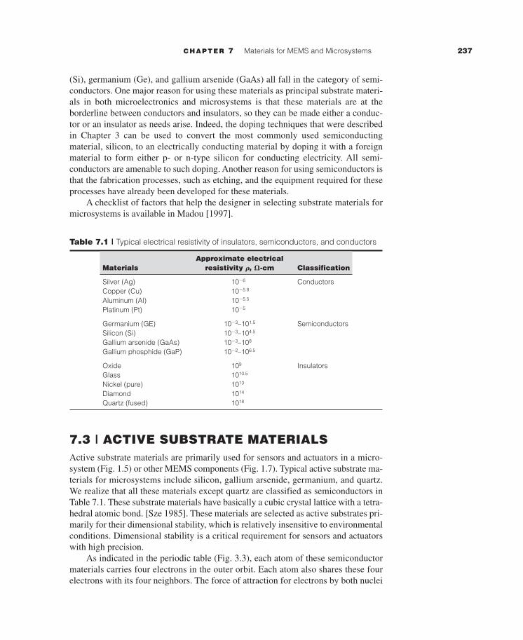
Table 7.1 presents a group of materials that are classified as electric insulators(or dielectrics), semiconductors, and conductors [Sze 1985]. The same referenceclassifies the insulators to have electrical resistivity � in the range of � � 108 �-cm;semiconductors with 10�3 �-cm � � � 108 �-cm; and conductors with � � 10 –3
�-cm. We will find that common substrate materials used in MEMS such as silicon
hsu93912_ch07.qxd 10/1/2001 12:46 PM Page 236
CHAPTER 7 Materials for MEMS and Microsystems 237
(Si), germanium (Ge), and gallium arsenide (GaAs) all fall in the category of semi-conductors. One major reason for using these materials as principal substrate materi-als in both microelectronics and microsystems is that these materials are at theborderline between conductors and insulators, so they can be made either a conduc-tor or an insulator as needs arise. Indeed, the doping techniques that were describedin Chapter 3 can be used to convert the most commonly used semiconductingmaterial, silicon, to an electrically conducting material by doping it with a foreignmaterial to form either p- or n-type silicon for conducting electricity. All semi-conductors are amenable to such doping. Another reason for using semiconductors isthat the fabrication processes, such as etching, and the equipment required for theseprocesses have already been developed for these materials.
A checklist of factors that help the designer in selecting substrate materials formicrosystems is available in Madou [1997].
Table 7.1 | Typical electrical resistivity of insulators, semiconductors, and conductors
Approximate electrical Materials resistivity �, �-cm Classification
Silver (Ag) 10�6 ConductorsCopper (Cu) 10�5.8
Aluminum (Al) 10�5.5
Platinum (Pt) 10�5
Germanium (GE) 10�3–101.5 SemiconductorsSilicon (Si) 10�3–104.5
Gallium arsenide (GaAs) 10�3–108
Gallium phosphide (GaP) 10�2–106.5
Oxide 109 InsulatorsGlass 1010.5
Nickel (pure) 1013
Diamond 1014
Quartz (fused) 1018
7.3 | ACTIVE SUBSTRATE MATERIALSActive substrate materials are primarily used for sensors and actuators in a micro-system (Fig. 1.5) or other MEMS components (Fig. 1.7). Typical active substrate ma-terials for microsystems include silicon, gallium arsenide, germanium, and quartz.We realize that all these materials except quartz are classified as semiconductors inTable 7.1. These substrate materials have basically a cubic crystal lattice with a tetra-hedral atomic bond. [Sze 1985]. These materials are selected as active substrates pri-marily for their dimensional stability, which is relatively insensitive to environmentalconditions. Dimensional stability is a critical requirement for sensors and actuatorswith high precision.
As indicated in the periodic table (Fig. 3.3), each atom of these semiconductormaterials carries four electrons in the outer orbit. Each atom also shares these fourelectrons with its four neighbors. The force of attraction for electrons by both nuclei
hsu93912_ch07.qxd 10/1/2001 12:46 PM Page 237
238 MEMS and Microsystems: Design and Manufacture
holds each pair of shared atoms together. They can be doped with foreign materialsto alter their electric conductivity as described in Section 3.5.
7.4 | SILICON AS A SUBSTRATE MATERIAL7.4.1 The Ideal Substrate for MEMS
Silicon is the most abundant material on earth. However, it almost always exists incompounds with other elements. Single-crystal silicon is the most widely used sub-strate material for MEMS and microsystems. The popularity of silicon for such ap-plication is primarily for the following reasons:
1. It is mechanically stable and it can be integrated into electronics on the samesubstrate. Electronics for signal transduction, such as a p- or n-typepiezoresistor, can be readily integrated with the Si substrate.
2. Silicon is almost an ideal structural material. It has about the same Young’smodulus as steel (about 2 � 105 MPa), but is as light as aluminum, with a massdensity of about 2.3 g/cm3. Materials with a high Young’s modulus can bettermaintain a linear relationship between applied load and the induceddeformations.
3. It has a melting point at 1400°C, which is about twice as high as that ofaluminum. This high melting point makes silicon dimensionally stable even atelevated temperature.
4. Its thermal expansion coefficient is about 8 times smaller than that of steel, andis more than 10 times smaller than that of aluminum.
5. Above all, silicon shows virtually no mechanical hysteresis. It is thus an idealcandidate material for sensors and actuators. Moreover, silicon wafers areextremely flat and accept coatings and additional thin-film layers for buildingmicrostructural geometry or conducting electricity.
6. There is a greater flexibility in design and manufacture with silicon than withother substrate materials. Treatments and fabrication processes for siliconsubstrates are well established and documented.
7.4.2 Single-Crystal Silicon and Wafers
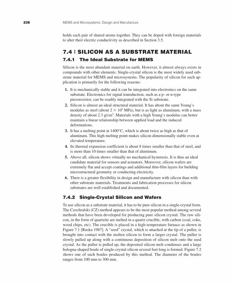
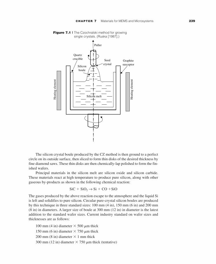
To use silicon as a substrate material, it has to be pure silicon in a single-crystal form.The Czochralski (CZ) method appears to be the most popular method among severalmethods that have been developed for producing pure silicon crystal. The raw sili-con, in the form of quartzite are melted in a quartz crucible, with carbon (coal, coke,wood chips, etc). The crucible is placed in a high-temperature furnace as shown inFigure 7.1 [Ruska 1987]. A “seed” crystal, which is attached at the tip of a puller, isbrought into contact with the molten silicon to form a larger crystal. The puller isslowly pulled up along with a continuous deposition of silicon melt onto the seedcrystal. As the puller is pulled up, the deposited silicon melt condenses and a largebologna-shaped boule of single-crystal silicon several feet long is formed. Figure 7.2shows one of such boules produced by this method. The diameter of the boulesranges from 100 mm to 300 mm.
hsu93912_ch07.qxd 10/1/2001 12:46 PM Page 238
CHAPTER 7 Materials for MEMS and Microsystems 239
Figure 7.1 | The Czochralski method for growingsingle crystals. (Ruska [1987].)
The silicon crystal boule produced by the CZ method is then ground to a perfectcircle on its outside surface, then sliced to form thin disks of the desired thickness byfine diamond saws. These thin disks are then chemically-lap polished to form the fin-ished wafers.
Principal materials in the silicon melt are silicon oxide and silicon carbide.These materials react at high temperature to produce pure silicon, along with othergaseous by-products as shown in the following chemical reaction:
SiC � SiO2 → Si � CO �SiO
The gases produced by the above reaction escape to the atmosphere and the liquid Siis left and solidifies to pure silicon. Circular pure-crystal silicon boules are producedby this technique in three standard sizes: 100 mm (4 in), 150 mm (6 in) and 200 mm(8 in) in diameters. A larger size of boule at 300 mm (12 in) in diameter is the latestaddition to the standard wafer sizes. Current industry standard on wafer sizes andthicknesses are as follows:
100 mm (4 in) diameter � 500 m thick
150 mm (6 in) diameter � 750 m thick
200 mm (8 in) diameter � 1 mm thick
300 mm (12 in) diameter � 750 m thick (tentative)
Puller
Quartzcrucible
Siliconboule
Seedcrystal
Graphitesusceptor
Silicon melt
Hea
ting
elem
ent
Hea
ting
elem
ent
hsu93912_ch07.qxd 10/1/2001 12:46 PM Page 239
240 MEMS and Microsystems: Design and Manufacture
Figure 7.2 | A 300-mm single-crystalsilicon boule cooling on amaterial-handling device.
(Courtesy of MEMC Electronic Materials Inc., St. Peters, Missouri.)
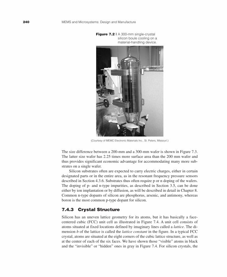
The size difference between a 200-mm and a 300-mm wafer is shown in Figure 7.3.The latter size wafer has 2.25 times more surface area than the 200 mm wafer andthus provides significant economic advantage for accommodating many more sub-strates on a single wafer.
Silicon substrates often are expected to carry electric charges, either in certaindesignated parts or in the entire area, as in the resonant frequency pressure sensorsdescribed in Section 4.3.6. Substrates thus often require p or n doping of the wafers.The doping of p- and n-type impurities, as described in Section 3.5, can be doneeither by ion implantation or by diffusion, as will be described in detail in Chapter 8.Common n-type dopants of silicon are phosphorus, arsenic, and antimony, whereasboron is the most common p-type dopant for silicon.
7.4.3 Crystal Structure
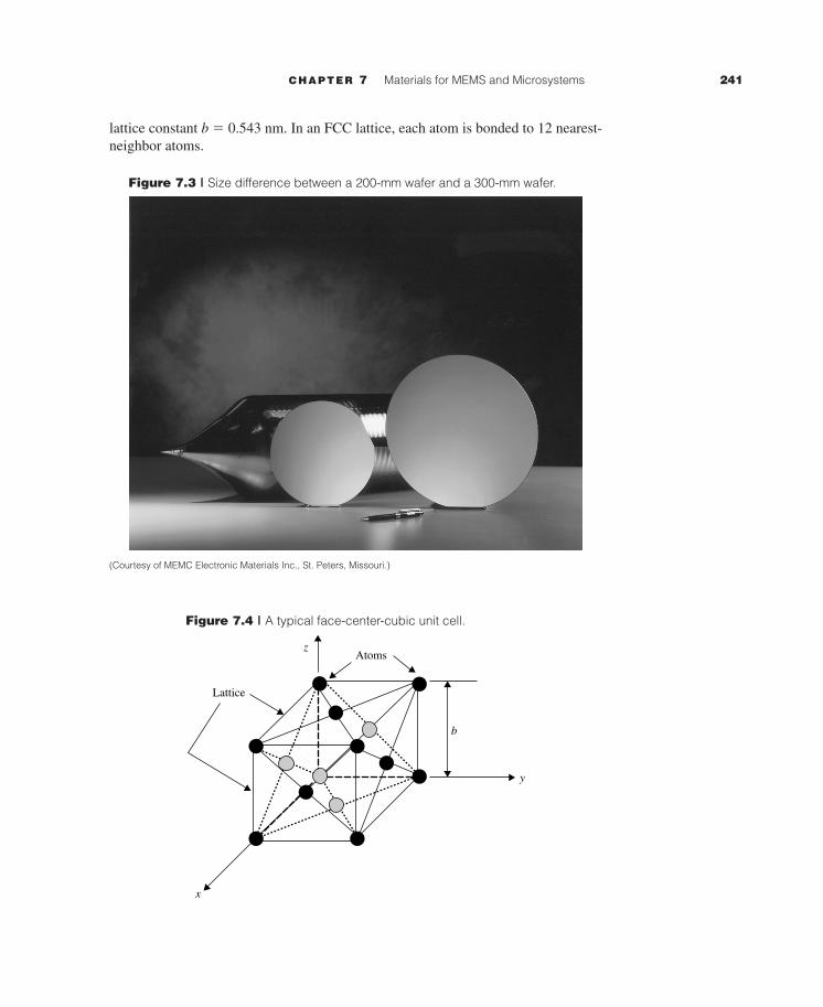
Silicon has an uneven lattice geometry for its atoms, but it has basically a face-centered cubic (FCC) unit cell as illustrated in Figure 7.4. A unit cell consists ofatoms situated at fixed locations defined by imaginary lines called a lattice. The di-mension b of the lattice is called the lattice constant in the figure. In a typical FCCcrystal, atoms are situated at the eight corners of the cubic lattice structure, as well asat the center of each of the six faces. We have shown those “visible” atoms in blackand the “invisible” or “hidden” ones in gray in Figure 7.4. For silicon crystals, the
hsu93912_ch07.qxd 10/1/2001 12:46 PM Page 240
CHAPTER 7 Materials for MEMS and Microsystems 241
lattice constant b 0.543 nm. In an FCC lattice, each atom is bonded to 12 nearest-neighbor atoms.
Figure 7.3 | Size difference between a 200-mm wafer and a 300-mm wafer.
(Courtesy of MEMC Electronic Materials Inc., St. Peters, Missouri.)
Figure 7.4 | A typical face-center-cubic unit cell.
Atoms
Lattice
b
y
x
z
hsu93912_ch07.qxd 10/1/2001 12:46 PM Page 241
242 MEMS and Microsystems: Design and Manufacture
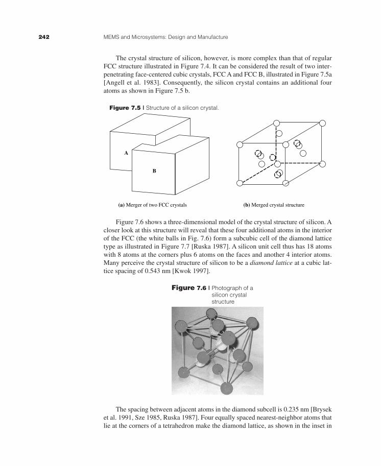
The crystal structure of silicon, however, is more complex than that of regularFCC structure illustrated in Figure 7.4. It can be considered the result of two inter-penetrating face-centered cubic crystals, FCC A and FCC B, illustrated in Figure 7.5a[Angell et al. 1983]. Consequently, the silicon crystal contains an additional fouratoms as shown in Figure 7.5 b.
Figure 7.5 | Structure of a silicon crystal.
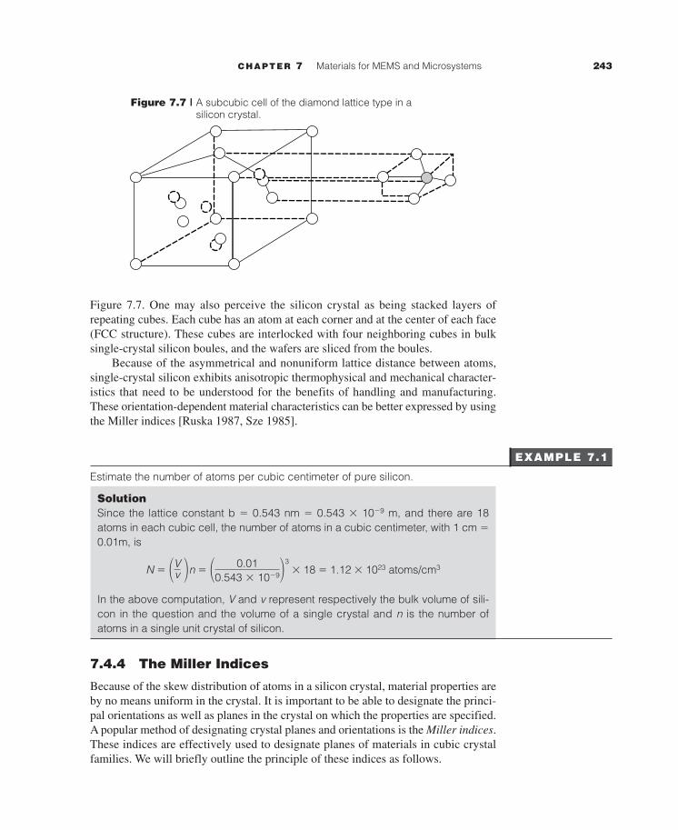
Figure 7.6 shows a three-dimensional model of the crystal structure of silicon. Acloser look at this structure will reveal that these four additional atoms in the interiorof the FCC (the white balls in Fig. 7.6) form a subcubic cell of the diamond latticetype as illustrated in Figure 7.7 [Ruska 1987]. A silicon unit cell thus has 18 atomswith 8 atoms at the corners plus 6 atoms on the faces and another 4 interior atoms.Many perceive the crystal structure of silicon to be a diamond lattice at a cubic lat-tice spacing of 0.543 nm [Kwok 1997].
The spacing between adjacent atoms in the diamond subcell is 0.235 nm [Bryseket al. 1991, Sze 1985, Ruska 1987]. Four equally spaced nearest-neighbor atoms thatlie at the corners of a tetrahedron make the diamond lattice, as shown in the inset in
(a) Merger of two FCC crystals
A
B
(b) Merged crystal structure
Figure 7.6 | Photograph of asilicon crystalstructure
hsu93912_ch07.qxd 10/1/2001 12:46 PM Page 242
CHAPTER 7 Materials for MEMS and Microsystems 243
Figure 7.7. One may also perceive the silicon crystal as being stacked layers ofrepeating cubes. Each cube has an atom at each corner and at the center of each face(FCC structure). These cubes are interlocked with four neighboring cubes in bulksingle-crystal silicon boules, and the wafers are sliced from the boules.
Because of the asymmetrical and nonuniform lattice distance between atoms,single-crystal silicon exhibits anisotropic thermophysical and mechanical character-istics that need to be understood for the benefits of handling and manufacturing.These orientation-dependent material characteristics can be better expressed by usingthe Miller indices [Ruska 1987, Sze 1985].
Estimate the number of atoms per cubic centimeter of pure silicon.
SolutionSince the lattice constant b 0.543 nm 0.543 � 10�9 m, and there are 18atoms in each cubic cell, the number of atoms in a cubic centimeter, with 1 cm 0.01m, is
N n � 18 1.12 � 1023 atoms/cm3
In the above computation, V and v represent respectively the bulk volume of sili-con in the question and the volume of a single crystal and n is the number ofatoms in a single unit crystal of silicon.
7.4.4 The Miller Indices
Because of the skew distribution of atoms in a silicon crystal, material properties areby no means uniform in the crystal. It is important to be able to designate the princi-pal orientations as well as planes in the crystal on which the properties are specified.A popular method of designating crystal planes and orientations is the Miller indices.These indices are effectively used to designate planes of materials in cubic crystalfamilies. We will briefly outline the principle of these indices as follows.
� 0.010.543 � 10�9�3�Vv �
EXAMPLE 7.1
Figure 7.7 | A subcubic cell of the diamond lattice type in asilicon crystal.
hsu93912_ch07.qxd 10/1/2001 12:46 PM Page 243
244 MEMS and Microsystems: Design and Manufacture
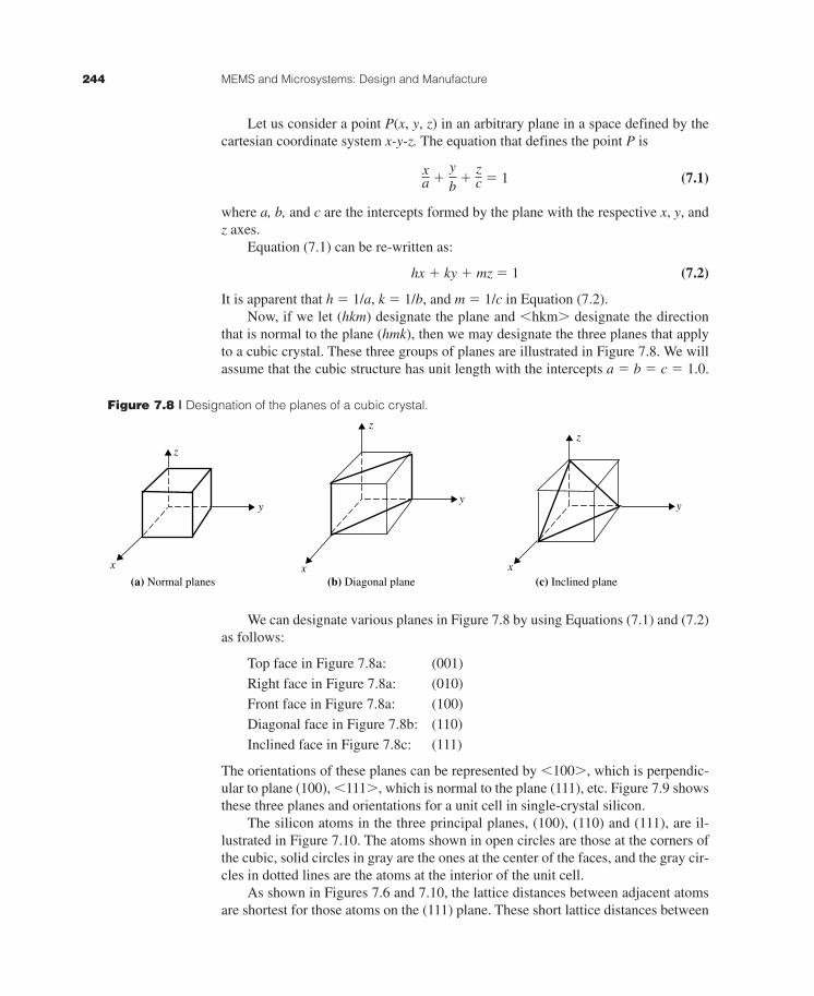
Let us consider a point P(x, y, z) in an arbitrary plane in a space defined by thecartesian coordinate system x-y-z. The equation that defines the point P is
� � 1 (7.1)
where a, b, and c are the intercepts formed by the plane with the respective x, y, andz axes.
Equation (7.1) can be re-written as:
hx � ky � mz 1 (7.2)
It is apparent that h 1/a, k 1/b, and m 1/c in Equation (7.2).Now, if we let (hkm) designate the plane and �hkm� designate the direction
that is normal to the plane (hmk), then we may designate the three planes that applyto a cubic crystal. These three groups of planes are illustrated in Figure 7.8. We willassume that the cubic structure has unit length with the intercepts a b c 1.0.
We can designate various planes in Figure 7.8 by using Equations (7.1) and (7.2)as follows:
Top face in Figure 7.8a: (001)
Right face in Figure 7.8a: (010)
Front face in Figure 7.8a: (100)
Diagonal face in Figure 7.8b: (110)
Inclined face in Figure 7.8c: (111)
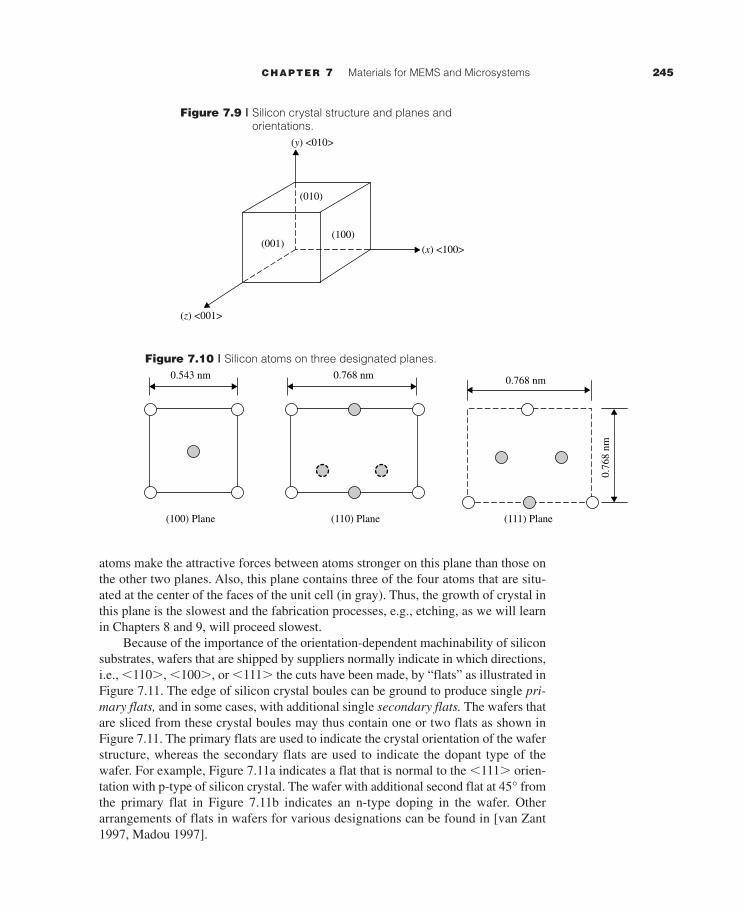
The orientations of these planes can be represented by �100�, which is perpendic-ular to plane (100), �111�, which is normal to the plane (111), etc. Figure 7.9 showsthese three planes and orientations for a unit cell in single-crystal silicon.
The silicon atoms in the three principal planes, (100), (110) and (111), are il-lustrated in Figure 7.10. The atoms shown in open circles are those at the corners ofthe cubic, solid circles in gray are the ones at the center of the faces, and the gray cir-cles in dotted lines are the atoms at the interior of the unit cell.
As shown in Figures 7.6 and 7.10, the lattice distances between adjacent atomsare shortest for those atoms on the (111) plane. These short lattice distances between
zc
yb
xa
x
z
zz
yy
y
x x(a) Normal planes (b) Diagonal plane (c) Inclined plane
Figure 7.8 | Designation of the planes of a cubic crystal.
hsu93912_ch07.qxd 10/1/2001 12:46 PM Page 244
CHAPTER 7 Materials for MEMS and Microsystems 245
atoms make the attractive forces between atoms stronger on this plane than those onthe other two planes. Also, this plane contains three of the four atoms that are situ-ated at the center of the faces of the unit cell (in gray). Thus, the growth of crystal inthis plane is the slowest and the fabrication processes, e.g., etching, as we will learnin Chapters 8 and 9, will proceed slowest.
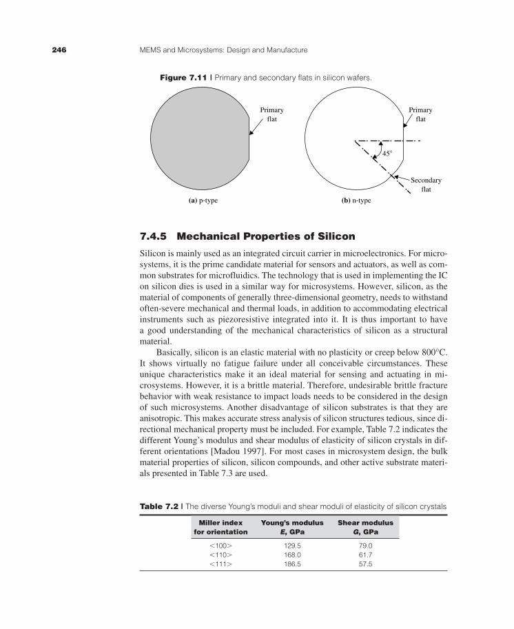
Because of the importance of the orientation-dependent machinability of siliconsubstrates, wafers that are shipped by suppliers normally indicate in which directions,i.e., �110�, �100�, or �111� the cuts have been made, by “flats” as illustrated inFigure 7.11. The edge of silicon crystal boules can be ground to produce single pri-mary flats, and in some cases, with additional single secondary flats. The wafers thatare sliced from these crystal boules may thus contain one or two flats as shown inFigure 7.11. The primary flats are used to indicate the crystal orientation of the waferstructure, whereas the secondary flats are used to indicate the dopant type of thewafer. For example, Figure 7.11a indicates a flat that is normal to the �111� orien-tation with p-type of silicon crystal. The wafer with additional second flat at 45° fromthe primary flat in Figure 7.11b indicates an n-type doping in the wafer. Otherarrangements of flats in wafers for various designations can be found in [van Zant1997, Madou 1997].
0.543 nm
(100) Plane (110) Plane (111) Plane
0.768 nm 0.768 nm
0.76
8 nm
Figure 7.10 | Silicon atoms on three designated planes.
(y) <010>
(x) <100>
(z) <001>
(001)(100)
(010)
Figure 7.9 | Silicon crystal structure and planes andorientations.
hsu93912_ch07.qxd 10/1/2001 12:46 PM Page 245
246 MEMS and Microsystems: Design and Manufacture
Figure 7.11 | Primary and secondary flats in silicon wafers.
7.4.5 Mechanical Properties of Silicon
Silicon is mainly used as an integrated circuit carrier in microelectronics. For micro-systems, it is the prime candidate material for sensors and actuators, as well as com-mon substrates for microfluidics. The technology that is used in implementing the ICon silicon dies is used in a similar way for microsystems. However, silicon, as thematerial of components of generally three-dimensional geometry, needs to withstandoften-severe mechanical and thermal loads, in addition to accommodating electricalinstruments such as piezoresistive integrated into it. It is thus important to havea good understanding of the mechanical characteristics of silicon as a structuralmaterial.
Basically, silicon is an elastic material with no plasticity or creep below 800°C.It shows virtually no fatigue failure under all conceivable circumstances. Theseunique characteristics make it an ideal material for sensing and actuating in mi-crosystems. However, it is a brittle material. Therefore, undesirable brittle fracturebehavior with weak resistance to impact loads needs to be considered in the designof such microsystems. Another disadvantage of silicon substrates is that they areanisotropic. This makes accurate stress analysis of silicon structures tedious, since di-rectional mechanical property must be included. For example, Table 7.2 indicates thedifferent Young’s modulus and shear modulus of elasticity of silicon crystals in dif-ferent orientations [Madou 1997]. For most cases in microsystem design, the bulkmaterial properties of silicon, silicon compounds, and other active substrate materi-als presented in Table 7.3 are used.
Table 7.2 | The diverse Young’s moduli and shear moduli of elasticity of silicon crystals
Miller index Young’s modulus Shear modulus for orientation E, GPa G, GPa
�100� 129.5 79.0�110� 168.0 61.7�111� 186.5 57.5
Primaryflat
(a) p-type
Primaryflat
(b) n-type
Secondaryflat
45�
hsu93912_ch07.qxd 10/1/2001 12:46 PM Page 246
CHAPTER 7 Materials for MEMS and Microsystems 247
Table 7.3 | Mechanical and thermophysical properties of MEMS materials*
�y, E, �, c, k, �, TM, Material 109 N/m2 1011 N/m2 g/cm3 J/g-°C W/cm-°C 10�6/°C °C
Si 7.00 1.90 2.30 0.70 1.57 2.33 1400SiC 21.00 7.00 3.20 0.67 3.50 3.30 2300Si3N4 14.00 3.85 3.10 0.69 0.19 0.80 1930SiO2 8.40 0.73 2.27 1.00 0.014 0.50 1700Aluminum 0.17 0.70 2.70 0.942 2.36 25 660Stainless steel 2.10 2.00 7.90 0.47 0.329 17.30 1500Copper 0.07 0.11 8.9 0.386 3.93 16.56 1080GaAs 2.70 0.75 5.30 0.35 0.50 6.86 1238Ge 1.03 5.32 0.31 0.60 5.80 937Quartz 0.5-0.7 0.76-0.97 2.66 0.82-1.20 0.067.0.12 7.10 1710
*Principal source for semiconductor material properties: Fundamentals of Microfabrication, Marc Madou,CRC Press, 1997
Legend: �y yield strength, E Young’s modulus, � mass density, c specific heat, k thermal conductivity, coefficient of thermal expansion, TM melting point.
As indicated in Chapter 5, the thermal diffusivity of a material is a measure of howfast heat can flow in the material. List the thermal diffusivities of silicon, silicon di-oxide, aluminum, and copper, and make an observation on the results.
SolutionThe thermal diffusivity is a function of several properties of the material asshown in Equation (5.39):
where the properties k, �, and c for the four materials are given in Table 7.3. Theyare listed in slightly different units in Table 7.4.
Table 7.4 | Thermal diffusivity of selected materials for microsystems
k, �, c, Thermal diffusivity,Material J/sce-m-°C g/m3 J/g-°C �, m2/s
Si 157 2.3 � 106 0.7 97.52 � 10�6
SiO2 1.4 2.27 � 106 1.0 0.62 � 10�6
Aluminum 236 2.7 � 106 0.94 93 � 10�6
Copper 393 8.9 � 106 0.386 114.4 � 10�6
By substituting the material properties tabulated in the three left columns inTable 7.4 into Equation (5.39), we can compute the thermal diffusivities of the ma-terials as indicated in the right column in the same table. It is not surprising toobserve that copper has the highest thermal diffusivity, whereas silicon and alu-minum have about the same value. Useful information from this exercise is that sil-icon oxide conducts heat more than 150 times slower than silicon and aluminum.
k�c
EXAMPLE 7.2
hsu93912_ch07.qxd 10/1/2001 12:46 PM Page 247
248 MEMS and Microsystems: Design and Manufacture
We may thus conclude that copper films are the best material for fast heat trans-mission in microsystems, whereas silicon dioxide can be used as an effectivethermal barrier.
7.5 | SILICON COMPOUNDSThree silicon compounds are often used in microsystems: silicon dioxide, SiO2; sili-con carbide, SiC; and silicon nitride, Si3N4. We will take a brief look at each of thesecompounds as to the roles they play in microsystems.
7.5.1 Silicon Dioxide
There are three principal uses of silicon oxide in microsystems: (1) as a thermal andelectric insulator (see Table 7.1 for the low electric resistivity of oxides), (2) as amask in the etching of silicon substrates, and (3) as a sacrificial layer in surfacemicromachining, as will be described in Chapter 9. Silicon oxide has much strongerresistance to most etchants than silicon. Important properties of silicon oxide arelisted in Table 7.5.
Table 7.5 | Properties of silicon dioxide
Properties Values
Density, g/cm3 2.27Resistivity, �-cm �1016
Relative permittivity 3.9Melting point, °C �1700Specific heat, J/g-°C 1.0Thermal conductivity, W/cm-°C 0.014Coefficient of thermal expansion, ppm/ ° C 0.5
Source: Ruska [1987].
Silicon dioxide can be produced by heating silicon in an oxidant such as oxygenwith or without steam. Chemical reactions for such processes are:
Si � O2 → SiO2 (7.3)
for “dry” oxidation, and
Si � 2H2O → SiO2 � 2H2 (7.4)
for “wet” oxidation in steam.Oxidation is effectively a diffusion process, as described in Chapter 3. There-
fore, the rate of oxidation can be controlled by similar techniques used for most otherdiffusion processes. Typical diffusivity of silicon dioxide at 900°C in dry oxidationis 4 � 10�19 cm2/s for arsenic-doped (n-type) silicon and 3 � 10�19 cm2/s for boron-doped (p-type) silicon [Sze 1985]. The process can be accelerated to much faster
hsu93912_ch07.qxd 10/1/2001 12:46 PM Page 248
CHAPTER 7 Materials for MEMS and Microsystems 249
rates by the presence of steam; the highly activated H2O molecules enhance theprocess. As in all diffusion processes, the diffusivity of the substance to be diffusedinto the base material is the key parameter for the effectiveness of the diffusionprocess.
7.5.2 Silicon Carbide
The principal application of silicon carbide (SiC) in microsystems is its dimensionaland chemical stability at high temperatures. It has very strong resistance to oxidationeven at very high temperatures. Thin films of silicon carbide are often deposited overMEMS components to protect them from extreme temperature. Another attraction ofusing SiC in MEMS is that dry etching (to be described in Chapters 8 and 9) withaluminum masks can easily pattern the thin SiC film. The patterned SiC film can fur-ther be used as a passivation layer (protective layer) in micromachining for the un-derlying silicon substrate, as SiC can resist common etchants such as KOH and HF.
Silicon carbide is a by-product in the process of producing single crystal siliconboules as described in Section 7.4.2. As silicon exists in the raw materials of carbon(coal, coke, wood chips, etc.), the intense heating of these materials in the electric arcfurnace results in SiC sinking to the bottom of the crucible. Silicon carbide films canbe produced by various deposition techniques. Pertinent thermophysical properties ofSiC are given in Table 7.3.
7.5.3 Silicon Nitride
Silicon nitride (Si3N4) has many superior properties that are attractive for MEMS andmicrosystems. It provides an excellent barrier to diffusion of water and ions such assodium. Its ultrastrong resistance to oxidation and many etchants makes it suitablefor masks for deep etching. Applications of silicon nitride include optical wave-guides, encapsulants to prevent diffusion of water and other toxic fluids into the sub-strate. It is also used as high-strength electric insulators and ion implantation masks.
Silicon nitride can be produced from silicon-containing gases and NH3 in thefollowing reaction:
3SiCl2H2 � 4 NH3 → Si3N4 � 6HCl � 6H2 (7.5)
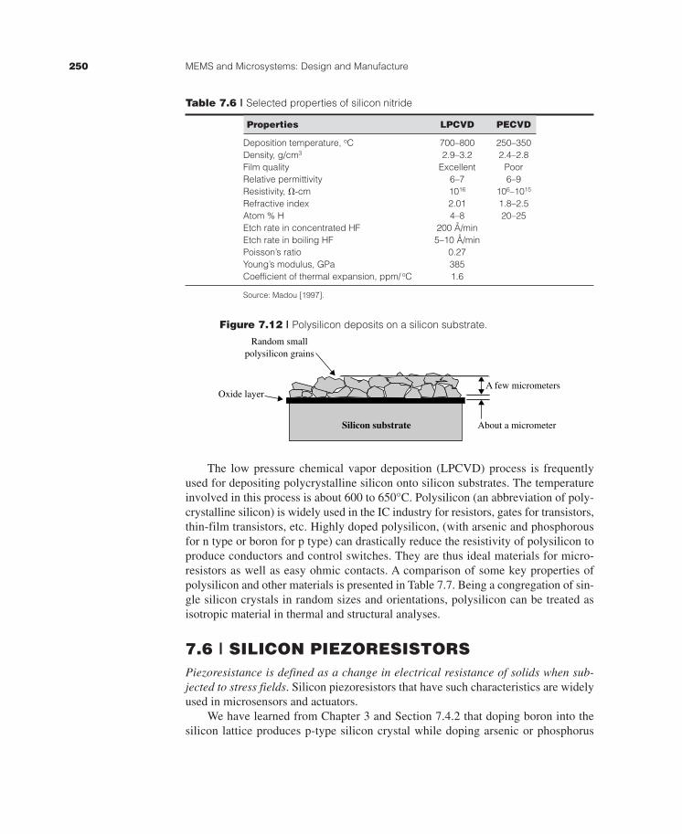
Selected properties of silicon nitride are listed in Table 7.6. Both chemical vapordeposition processes [low-pressure chemical vapor deposition (LPCVD) and theplasma-enhanced chemical vapor deposition (PECVD)] in Table 7.6 will be de-scribed in detail in Chapter 8. Additional material properties are given in Table 7.3.
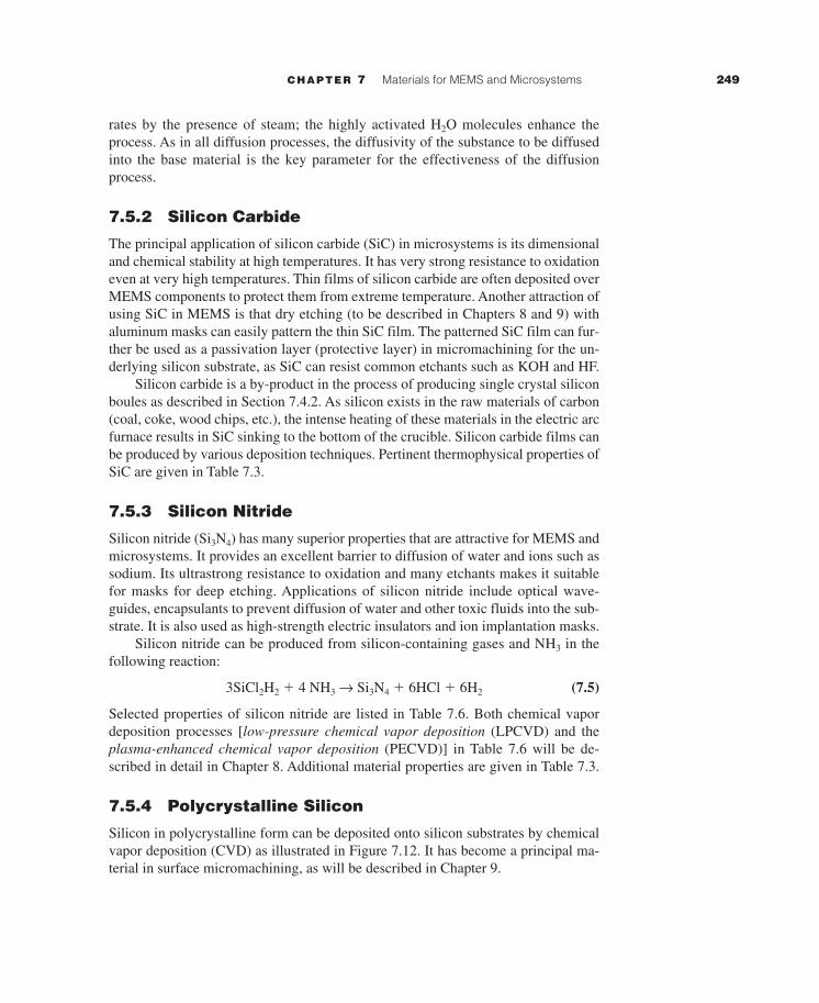
7.5.4 Polycrystalline Silicon
Silicon in polycrystalline form can be deposited onto silicon substrates by chemicalvapor deposition (CVD) as illustrated in Figure 7.12. It has become a principal ma-terial in surface micromachining, as will be described in Chapter 9.
hsu93912_ch07.qxd 10/1/2001 12:46 PM Page 249
250 MEMS and Microsystems: Design and Manufacture
Figure 7.12 | Polysilicon deposits on a silicon substrate.
The low pressure chemical vapor deposition (LPCVD) process is frequentlyused for depositing polycrystalline silicon onto silicon substrates. The temperatureinvolved in this process is about 600 to 650°C. Polysilicon (an abbreviation of poly-crystalline silicon) is widely used in the IC industry for resistors, gates for transistors,thin-film transistors, etc. Highly doped polysilicon, (with arsenic and phosphorousfor n type or boron for p type) can drastically reduce the resistivity of polysilicon toproduce conductors and control switches. They are thus ideal materials for micro-resistors as well as easy ohmic contacts. A comparison of some key properties ofpolysilicon and other materials is presented in Table 7.7. Being a congregation of sin-gle silicon crystals in random sizes and orientations, polysilicon can be treated asisotropic material in thermal and structural analyses.
7.6 | SILICON PIEZORESISTORSPiezoresistance is defined as a change in electrical resistance of solids when sub-jected to stress fields. Silicon piezoresistors that have such characteristics are widelyused in microsensors and actuators.
We have learned from Chapter 3 and Section 7.4.2 that doping boron into thesilicon lattice produces p-type silicon crystal while doping arsenic or phosphorus
Random smallpolysilicon grains
Oxide layer
About a micrometerSilicon substrate
A few micrometers
Table 7.6 | Selected properties of silicon nitride
Properties LPCVD PECVD
Deposition temperature, oC 700–800 250–350Density, g/cm3 2.9–3.2 2.4–2.8Film quality Excellent PoorRelative permittivity 6–7 6–9Resistivity, �-cm 1016 106–1015
Refractive index 2.01 1.8–2.5Atom % H 4–8 20–25Etch rate in concentrated HF 200 Å/minEtch rate in boiling HF 5–10 Å/minPoisson’s ratio 0.27Young’s modulus, GPa 385Coefficient of thermal expansion, ppm/ oC 1.6
Source: Madou [1997].
hsu93912_ch07.qxd 10/1/2001 12:46 PM Page 250
CHAPTER 7 Materials for MEMS and Microsystems 251
results in n-type silicon. Both p- and n-type silicon exhibit excellent piezoresistiveeffect. Charles Smith in 1954 discovered the piezoresistance of p- and n-type silicon.
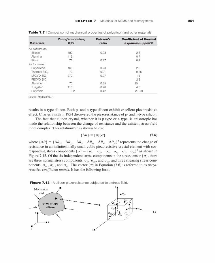
The fact that silicon crystal, whether it is p type or n type, is anisotropic hasmade the relationship between the change of resistance and the existent stress fieldmore complex. This relationship is shown below:
{�R} [�]{�} (7.6)
where {�R} {�Rxx �Ryy �Rzz �Rxy �Rxz �Ryz}T represents the change ofresistance in an infinitesimally small cubic piezoresistive crystal element with cor-responding stress components {�} {�xx �yy �zz �xy �xz �yz}T as shown inFigure 7.13. Of the six independent stress components in the stress tensor {�}, thereare three normal stress components, �xx , �yy , and �zz , and three shearing stress com-ponents, �xy , �xz , and �yz . The vector [�] in Equation (7.6) is referred to as piezo-resistive coefficient matrix. It has the following form:
Figure 7.13 | A silicon piezoresistance subjected to a stress field.
y
y
yz
Mechanicalload
x
x
p- or n-typesilicon
z z
σzyσ
zzσzxσ xzσ
xxσ
xzσyxσ
yyσ
Table 7.7 | Comparison of mechanical properties of polysilicon and other materials
Young’s modulus, Poisson’s Coefficient of thermal Materials GPa ratio expansion, ppm/oC
As substrates:Silicon 190 0.23 2.6Alumina 415 8.7Silica 73 0.17 0.4
As thin films:Polysilicon 160 0.23 2.8Thermal SiO2 70 0.2 0.35LPCVD SiO2 270 0.27 1.6PECVD SiO2 2.3Aluminum 70 0.35 25Tungsten 410 0.28 4.3Polymide 3.2 0.42 20–70
Source: Madou [1997].
hsu93912_ch07.qxd 10/1/2001 12:46 PM Page 251
252 MEMS and Microsystems: Design and Manufacture
[�] � � (7.7)
We notice from Equation (7.7) that only three coefficients, �11, �12, and �44, appearin the matrix. By expanding the matrix equation in Equation (7.6) with the appropri-ate piezoresistive coefficients in Equation (7.7), we will have the following relations:
�Rxx �11�xx � �12 (�yy � �zz )
�Ryy �11�yy � �12 (�xx � �zz )
�Rzz �11�zz � �12 (�xx � �yy )
�Rxy �44�xy
�Rxz �44�xz
�Ryz �44�yz
It is thus apparent that the coefficients �11 and �12 are associated with the nor-mal stress components, whereas the coefficient �44 is related to the shearing stresscomponents.
The actual values of these three coefficients depend on the angles of the piezo-resistor with respect to the silicon crystal lattice. The values of these coefficients atroom temperature are given in Table 7.8.
Table 7.8 | Resistivity and piezoresistive coefficients of silicon at room temperature in�100� orientation
Materials Resistivity, �-cm �11* �12* �44*
p silicon 7.8 �6.6 �1.1 �138.1n silicon 11.7 �102.2 �53.4 �13.6
*in 10�12 cm2/dyne or in 10�11 m2/N (or Pa�1)
Source: French and Evans [1988].
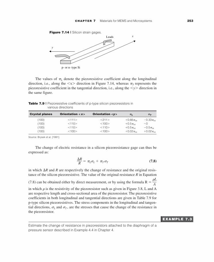
Equation (7.6) and the situation illustrated in Figure 7.13, of course, representgeneral cases of piezoresistive crystals in a three-dimensional geometry. In almost allapplications in MEMS and microsystems, silicon piezoresistors exist in the form ofthin strips such as illustrated in Figure 7.14. In such cases, only the in-plane stressesin the x and y directions need to be accounted for.
We will realize from Table 7.8 that the maximum piezoresistive coefficient forp-type silicon is �44 �138.1 � 10�11 Pa�1, and the maximum coefficient for then-type silicon is �11 �102.2 � 10�11 Pa�1. Thus, many silicon piezoresistors aremade of p-type material with boron as the dopant. Table 7.9 presents the values ofpiezoresistive coefficients for the p-type silicon piezoresistors made in various crys-tal planes [Brysek et al. 1991].
�11�12�12000
�12�11�12000
�12�12�11000
000�4400
0000�440
00000�44
hsu93912_ch07.qxd 10/1/2001 12:46 PM Page 252
CHAPTER 7 Materials for MEMS and Microsystems 253
The values of �L denote the piezoresistive coefficient along the longitudinaldirection, i.e., along the �x� direction in Figure 7.14, whereas �T represents thepiezoresistive coefficient in the tangential direction, i.e., along the �y� direction inthe same figure.
Table 7.9 | Piezoresistive coefficients of p-type silicon piezoresistors invarious directions
Crystal planes Orientation <x> Orientation <y> �L �T
(100) �111� �211� �0.66�44 �0.33�44
(100) �110� �100� �0.5�44 �0(100) �110� �110� �0.5�44 �0.5�44
(100) �100� �100� �0.02�44 �0.02�44
Source: Brysek et al. [1991].
The change of electric resistance in a silicon piezoresistance gage can thus beexpressed as:
�L�L � �T �T (7.8)
in which �R and R are respectively the change of resistance and the original resis-tance of the silicon piezoresistive. The value of the original resistance R in Equation
(7.8) can be obtained either by direct measurement, or by using the formula R
in which � is the resistivity of the piezoresistor such as given in Figure 3.8, L and Aare respective length and cross-sectional area of the piezoresistor. The piezoresistivecoefficients in both longitudinal and tangential directions are given in Table 7.9 forp-type silicon piezoresistives. The stress components in the longitudinal and tangen-tial directions, �L and �T , are the stresses that cause the change of the resistance inthe piezoresistor.
Estimate the change of resistance in piezoresistors attached to the diaphragm of apressure sensor described in Example 4.4 in Chapter 4.
�LA
�RR
y
xLeads
p- or n- type Si
Figure 7.14 | Silicon strain gages.
EXAMPLE 7.3
hsu93912_ch07.qxd 10/1/2001 12:46 PM Page 253
254 MEMS and Microsystems: Design and Manufacture
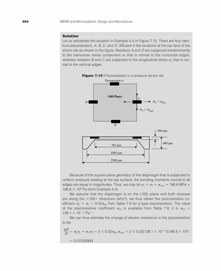
SolutionLet us reillustrate the situation in Example 4.4 in Figure 7.15. There are four iden-tical piezoresistors, A, B, C, and D, diffused in the locations at the top face of thesilicon die as shown in the figure. Resistors A and D are subjected predominantlyto the transverse stress component �T that is normal to the horizontal edges,whereas resistors B and C are subjected to the longitudinal stress �L that is nor-mal to the vertical edges.
Figure 7.15 | Piezoresistors in a pressure sensor die.
Because of the square plane geometry of the diaphragm that is subjected touniform pressure loading at the top surface, the bending moments normal to alledges are equal in magnitudes. Thus, we may let �L �T �max 186.8 MPa 186.8 � 106 Pa (from Example 4.4).
We assume that the diaphragm is on the (100) plane and both stressesare along the �100� directions (why?), we thus obtain the piezoresistive co-efficient �L �T 0.02�44 from Table 7.9 for p-type piezoresistors. The valueof the piezoresistive coefficient �44 is available from Table 7.8; it is �44
138.1 � 10�11 Pa�1.We can thus estimate the change of electric resistance in the piezoresistors
to be:
�L�L � �T �T 2 � 0.02�44 �max 2 � 0.02(138.1 � 10�11)(186.8 � 106)
0.01032�/�
�RR
T maxσ σ
L maxσ σC
D
B
Piezoresistor A
(100 Plane)
266 µm
480 µm783 µm
1085 µm
2500 µm
hsu93912_ch07.qxd 10/1/2001 12:46 PM Page 254
CHAPTER 7 Materials for MEMS and Microsystems 255
Determining the net change of resistance in the resistors requires knowledge ofthe length of the resistor in the stress-free state and the resistivity of the resistormaterial as given in Figure 3.8.
One major drawback of silicon piezoresistors is the strong temperature depen-dence of their piezoresistivity. The sensitivity of piezoresistivity to the applied stressdeteriorates rapidly with increase of temperature. Table 7.10 presents the variation ofpiezoresistive coefficients with reference to those at room temperature.
Table 7.10 | Temperature dependence of resistivity and piezoresistivity of siliconpiezoresistors
Doping concentration, p-type TCR, p-type TCP, n-type TCR, n-type TCP,
1018/cm3 % per °C % per °C % per °C % per °C
5 0.0 �0.27 0.01 �0.2810 0.01 �0.27 0.05 �0.2730 0.06 �0.18 0.09 �0.18
100 0.17 �0.16 0.19 �0.12
Source: [French and Evans 1988].
TCR temperature coefficient of resistance; TCP temperature coefficient of piezoresistivity.
Take for example, a p-type silicon piezoresistor with a doping concentration of1019 per cm3; the loss of piezoresistivity is 0.27% per °C. The same piezoresistoroperating at 120°C would have lost (120 – 20) � 0.27% 27% of the value of thepiezoresistivity coefficient. Appropriate compensation for this loss must be consid-ered in the design of signal conditioning systems.
The doping concentration for piezoresistives normally should be kept below1019/cm3 because the piezoresistive coefficients drop considerably above this dose,and reverse breakdown becomes an issue.
7.7 | GALLIUM ARSENIDEGallium arsenide (GaAs) is a compound semiconductor. It is made of equal numbersof gallium and arsenic atoms. Because it is a compound, it is more complicated in lat-tice structure, with atoms of both constituents, and hence is more difficult to processthan silicon. However, GaAs is an excellent material for monolithic integration ofelectronic and photonic devices on a single substrate. The main reason that GaAs isa prime candidate material for photonic devices is its high mobility of electrons incomparison to other semiconducting materials, as shown in Table 7.11.
As we see from the table, GaAs has about 7 times higher electron mobility thansilicon. The high electron mobility in this material means it is easier for electric cur-rent to flow in the material. The photoelectronic effect, as illustrated in Section 2.2.4in Chapter 2, describes the electric current flow in a photoelectric material whenit is energized by incoming photons. GaAs, being a material with high mobility of
hsu93912_ch07.qxd 10/1/2001 12:46 PM Page 255
256 MEMS and Microsystems: Design and Manufacture
electrons, thus can better facilitate the electric current flow when it is energized byphoton sources.
Gallium arsenide is also a superior thermal insulator, with excellent dimensionalstability at high temperature. The negative aspect of this material is its low yieldstrength as indicated in Table 7.3. Its yield strength, at 2700 MPa, is only one-thirdof that of silicon. This makes GaAs less attractive for use as substrates in micro-systems. Because of its relatively low use in the microelectronics industry, GaAs ismuch more expensive than silicon.
In addition to the differences in thermophysical properties as indicated inTable 7.3, Table 7.12 gives a good comparison of these two substrate materials usedin microsystems.
Table 7.12 | A comparison of GaAs and silicon in micromachining
Properties GaAs Silicon
Optoelectronics Very good Not goodPiezoelectric effect Yes NoPiezoelectric coefficient, pN/ ° C 2.6 NilThermal conductivity Relatively low Relatively highCost High LowBonding to other substrates Difficult Relatively easyFracture Brittle, fragile Brittle, strongOperating temperature High LowOptimum operating temp., °C 460 300Physical stability Fair Very goodHardness, GPa 7 10Fracture strength, GPa 2.7 6
Source: Madou [1997].
7.8 | QUARTZQuartz is a compound of SiO2. The single-unit cell for quartz is in the shape of tetra-hedron with three oxygen atoms at the apexes at the base and one silicon atom at theother apex of the tetrahedron. The axis that is normal to the base plane is calledthe Z axis. The quartz crystal structure is made up of rings with six silicon atoms.
Quartz is close to being an ideal material for sensors because of its near absolutethermal dimensional stability. It is used in many piezoelectric devices in the market,
Table 7.11 | Electron mobility of selected materials at 300 K
Materials Electron mobility, m2/V-s
Aluminum 0.00435Copper 0.00136Silicon 0.145Gallium arsenide 0.850Silicon oxide �0Silicon nitride �0
Source: Kwok [1997].
hsu93912_ch07.qxd 10/1/2001 12:46 PM Page 256
CHAPTER 7 Materials for MEMS and Microsystems 257
as will be described in Section 7.9. Commercial applications of quartz crystals in-clude wristwatches, electronic filters, and resonators. Quartz is a desirable materialin microfluidics applications in biomedical analyses. It is inexpensive and it workswell in electrophoretic fluid transportation as described in Chapters 3 and 5 becauseof its excellent electric insulation properties. It is transparent to ultraviolet light,which often is used to detect the various species in the fluid.
Quartz is a material that is hard to machine. Diamond cutting is a commonmethod, although ultrasonic cutting has been used for more precise geometric trim-ming. It can be etched chemically by HF/NH4F into the desired shape. Quartz wafersup to 75 mm in diameter by 100 m thick are available commercially.
Quartz is even more dimensionally stable than silicon, especially at high tem-peratures. It offers more flexibility in geometry than silicon despite the difficulty inmachining. Some key properties are presented in Table 7.13.
Table 7.13 | Some properties of quartz
Temperature Properties Value �� Z Value ⊥ Z dependency
Thermal conductivity, cal/cm-s°/C 29 � 10�3 16 � 10�3 ↓ with TRelative permittivity 4.6 4.5 ↓ with TDensity, kg/m3 2.66 � 103 2.66 � 103
Coefficient of thermal expansion, ppm/ ° C 7.1 13.2 ↑ with TElectrical resistivity, �/cm 0.1 � 1015 20 � 1015 ↓ with TFracture strength, GPa 1.7 1.7 ↓ with THardness, GPa 12 12
Source: Madou [1997].
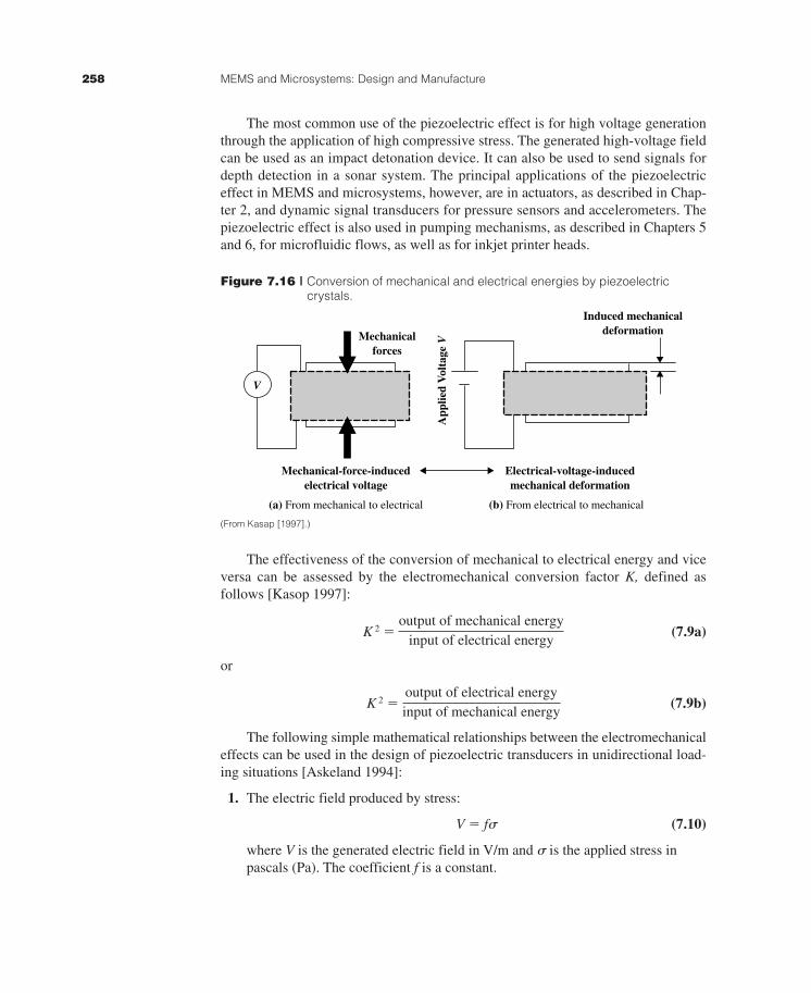
7.9 | PIEZOELECTRIC CRYSTALSOne of the most commonly used nonsemiconducting materials in MEMS andmicrosystems is piezoelectric crystals. Piezoelectric crystals are the solids of ceramiccompounds that can produce a voltage when a mechanical force is applied betweentheir faces. The reverse situation, that is the application of voltage to the crystal, canalso change its shape. This conversion of mechanical energy to electronic signals(i.e., voltage) and vice versa is illustrated in Figure 7.16. This unique material behav-ior is called the piezoelectric effect. Jacques and Pierre Curie discovered the piezo-electric effect in 1880. This effect exists in a number of natural crystals such asquartz, tourmaline, and sodium potassium tartrate, and quartz has been used inelectromechanical transducers for many years. There are many other synthesizedcrystals such as Rochelle salt (NaKC4H4O6-4H2O), barium titanate (BaTiO3), andlead zirconate titanate (PZT).
For a crystal to exhibit the piezoelectric effect, its structure should have nocenter of symmetry. A stress applied to such a crystal will alter the separation be-tween the positive and negative charge sites in each elementary cell, leading to a netpolarization at the crystal surface [Waanders 1991]. An electric field with voltagepotential is thus created in the crystal because of such polarization.
hsu93912_ch07.qxd 10/1/2001 12:46 PM Page 257
258 MEMS and Microsystems: Design and Manufacture
The most common use of the piezoelectric effect is for high voltage generationthrough the application of high compressive stress. The generated high-voltage fieldcan be used as an impact detonation device. It can also be used to send signals fordepth detection in a sonar system. The principal applications of the piezoelectriceffect in MEMS and microsystems, however, are in actuators, as described in Chap-ter 2, and dynamic signal transducers for pressure sensors and accelerometers. Thepiezoelectric effect is also used in pumping mechanisms, as described in Chapters 5and 6, for microfluidic flows, as well as for inkjet printer heads.
Figure 7.16 | Conversion of mechanical and electrical energies by piezoelectriccrystals.
(From Kasap [1997].)
The effectiveness of the conversion of mechanical to electrical energy and viceversa can be assessed by the electromechanical conversion factor K, defined asfollows [Kasop 1997]:
K 2 (7.9a)
or
K 2 (7.9b)
The following simple mathematical relationships between the electromechanicaleffects can be used in the design of piezoelectric transducers in unidirectional load-ing situations [Askeland 1994]:
1. The electric field produced by stress:
V f� (7.10)
where V is the generated electric field in V/m and � is the applied stress inpascals (Pa). The coefficient f is a constant.
output of electrical energyinput of mechanical energy
output of mechanical energyinput of electrical energy
Mechanicalforces
Mechanical-force-inducedelectrical voltage
Electrical-voltage-inducedmechanical deformation
(a) From mechanical to electrical (b) From electrical to mechanical
App
lied
Vol
tage
V
V
Induced mechanicaldeformation
hsu93912_ch07.qxd 10/1/2001 12:46 PM Page 258
CHAPTER 7 Materials for MEMS and Microsystems 259
2. The mechanical strain produced by the electric field:
� dV (7.11)
in which � is the induced strain and V is the applied electric field in V/m.The piezoelectric coefficient d for common piezoelectric crystals is given inTable 7.14.
The coefficients f and d in Equations (7.10) and (7.11) have the followingrelationship:
E (7.12)
where E is the Young’s modulus of the piezoelectric crystal.
Table 7.14 | Piezoelectric coefficients of selected materials
Coefficient d, Electromechanical Piezoelectric crystals 10�12 m/V conversion factor K
Quartz (crystal SiO2) 2.3 0.1Barium titanate (BaTiO3) 100–190 0.49Lead zirconate titanate, PZT (PbTi1 � x Zrx O3) 480 0.72PbZrTiO6 250PbNb2O6 80Rochelle salt (NaKC4H4O6-4H2O) 350 0.78Polyvinylidene fluoride, PVDF 18
Source: Kasap [1997], Askeland [1994].
A thin piezoelectric crystal film of PZT is used to transduce the signal in a micro-accelerometer with a cantilever beam made of silicon as described in Example 4.7.The accelerometer is designed for maximum acceleration/deceleration of 10g. ThePZT transducer is located at the support base of the cantilever beam wherethe maximum strain exists during the bending of the beam, as illustrated in Fig-ure 7.17. Determine the electrical voltage output from the PZT film at the maximumacceleration/deceleration of 10g.
1fd
EXAMPLE 7.4
A
A
PZT crystal(see detail A) Mass
m 10mg10 µm
1000 µm
10 µm
2 µm
4 µm
50 µm
View A–A Detail Amaxσ
maxσ
Figure 7.17 | Piezoelectric transducer in a beam-accelerometer.
hsu93912_ch07.qxd 10/1/2001 12:46 PM Page 259
260 MEMS and Microsystems: Design and Manufacture
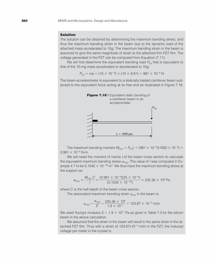
SolutionThe solution can be obtained by determining the maximum bending stress, andthus the maximum bending strain in the beam due to the dynamic load of theattached mass accelerated to 10g. The maximum bending strain in the beam isassumed to give the same magnitude of strain to the attached thin PZT film. Thevoltage generated in the PZT can be computed from Equation (7.11).
We will first determine the equivalent bending load Peq that is equivalent tothat of the 10-mg mass accelerated or decelerated to 10g:
Peq ma (10 � 10�6) � (10 � 9.81) 981 � 10�6 N
The beam-accelerometer is equivalent to a statically loaded cantilever beam sub-jected to the equivalent force acting at its free end as illustrated in Figure 7.18.
Figure 7.18 | Equivalent static bending ofa cantilever beam in anaccelerometer.
The maximum bending moment Mmax PeqL (981 � 10�6)(1000 � 10�6) 0.981 � 10�6 N-m.
We will need the moment of inertia I of the beam cross section to calculatethe equivalent maximum bending stress �max. The value of I was computed in Ex-ample 4.7 to be 0.1042 � 10�18 m4. We thus have the maximum bending stress atthe support as:
�max 235.36 � 106 Pa
where C is the half-depth of the beam cross section.The associated maximum bending strain �max in the beam is:
�max 123.87 � 10�5 m/m
We used Young’s modulus E 1.9 � 1011 Pa as given in Table 7.3 for the siliconbeam in the above calculation.
We assumed that the strain in the beam will result in the same strain in the at-tached PZT film. Thus with a strain of 123.87x10�5 m/m in the PZT, the inducedvoltage per meter in the crystal is:
235.36 � 106
1.9 � 1011
�max
E
(0.981 � 10�6)(25 � 10�6)(0.1042 � 10�18)
Mmax CI
Peq
L 1000 µm
hsu93912_ch07.qxd 10/1/2001 12:46 PM Page 260
CHAPTER 7 Materials for MEMS and Microsystems 261
V 0.258 � 107 V/m
We used the piezoelectric coefficient d 480 � 10�12 m/ V obtained fromTable 7.14 in the above computation.
Since the actual length of the PZT crystal attached to the beam is l 4 m,we will expect the total voltage generated by the transducer at 10g load to be:
v Vl (0.258 � 107)(4 � 10�6) 10.32 V
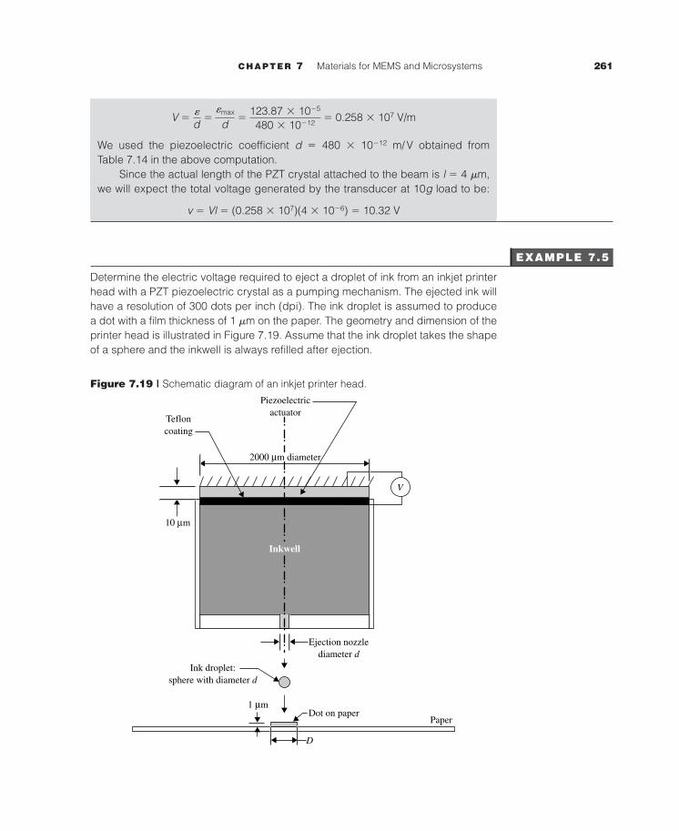
Determine the electric voltage required to eject a droplet of ink from an inkjet printerhead with a PZT piezoelectric crystal as a pumping mechanism. The ejected ink willhave a resolution of 300 dots per inch (dpi). The ink droplet is assumed to producea dot with a film thickness of 1 m on the paper. The geometry and dimension of theprinter head is illustrated in Figure 7.19. Assume that the ink droplet takes the shapeof a sphere and the inkwell is always refilled after ejection.
Figure 7.19 | Schematic diagram of an inkjet printer head.
V
Piezoelectricactuator
Tefloncoating
Ejection nozzlediameter d
D
Ink droplet:sphere with diameter d
Dot on paperPaper
10 µm
1 µm
Inkwell
2000 µm diameter
123.87 � 10�5
480 � 10�12
�max
d�d
EXAMPLE 7.5
hsu93912_ch07.qxd 10/1/2001 12:46 PM Page 261
262 MEMS and Microsystems: Design and Manufacture
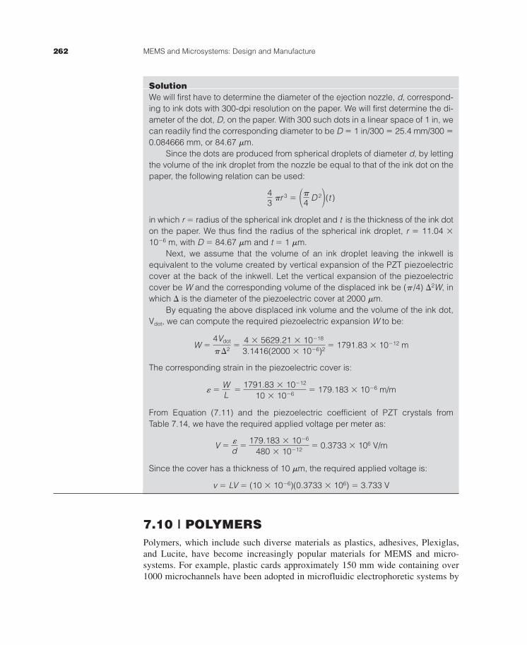
SolutionWe will first have to determine the diameter of the ejection nozzle, d, correspond-ing to ink dots with 300-dpi resolution on the paper. We will first determine the di-ameter of the dot, D, on the paper. With 300 such dots in a linear space of 1 in, wecan readily find the corresponding diameter to be D 1 in/300 25.4 mm/300 0.084666 mm, or 84.67 m.
Since the dots are produced from spherical droplets of diameter d, by lettingthe volume of the ink droplet from the nozzle be equal to that of the ink dot on thepaper, the following relation can be used:
�r 3 D 2 (t )
in which r radius of the spherical ink droplet and t is the thickness of the ink doton the paper. We thus find the radius of the spherical ink droplet, r 11.04 �10�6 m, with D 84.67 m and t 1 m.
Next, we assume that the volume of an ink droplet leaving the inkwell isequivalent to the volume created by vertical expansion of the PZT piezoelectriccover at the back of the inkwell. Let the vertical expansion of the piezoelectriccover be W and the corresponding volume of the displaced ink be (� /4) �2W, inwhich � is the diameter of the piezoelectric cover at 2000 m.
By equating the above displaced ink volume and the volume of the ink dot,Vdot, we can compute the required piezoelectric expansion W to be:
W 1791.83 � 10�12 m
The corresponding strain in the piezoelectric cover is:
� 179.183 � 10�6 m/m
From Equation (7.11) and the piezoelectric coefficient of PZT crystals fromTable 7.14, we have the required applied voltage per meter as:
V 0.3733 � 106 V/m
Since the cover has a thickness of 10 m, the required applied voltage is:
v LV (10 � 10�6)(0.3733 � 106) 3.733 V
7.10 | POLYMERSPolymers, which include such diverse materials as plastics, adhesives, Plexiglas,and Lucite, have become increasingly popular materials for MEMS and micro-systems. For example, plastic cards approximately 150 mm wide containing over1000 microchannels have been adopted in microfluidic electrophoretic systems by
179.183 � 10�6
480 � 10�12�d
1791.83 � 10�12
10 � 10�6WL
4 � 5629.21 � 10�18
3.1416(2000 � 10�6)2
4Vdot
� �2
���4
43
hsu93912_ch07.qxd 10/1/2001 12:46 PM Page 262
CHAPTER 7 Materials for MEMS and Microsystems 263
the biomedical industry [Lipman 1999] as described in Chapter 2. Epoxy resins andadhesives such as silicone rubber are customarily used in MEMS and microsystempackaging.
This type of material is made up of long chains of organic (mainly hydrocarbon)molecules. The combined molecules, i.e., polymer molecules, can be a few hundrednanometers long. Low mechanical strength, low melting point, and poor electricalconductivity characterize polymers. Thermoplastics and thermosets are two groupsof polymers that are commonly used for industrial products. Thermoplastics can beeasily formed to the desired shape for the specific product, whereas thermosets havebetter mechanical strength and temperature resistance up to 350°C. Because of therapid increase of applications in industrial products, polymers and polymerization,which is the process of producing various kinds of polymers, constitute a distinct en-gineering subject. It is not realistic to offer a complete list of available polymers andplastics, as well as the many polymerization processes in this chapter. What will bepresented in this section is information on the applications of polymers that are rele-vant to the design and packaging of MEMS and microsystems. Much of the materi-als presented here are available in greater detail in a special reference on polymersfor electronics and optoelectronics [Chilton and Goosey 1995].
7.10.1 Polymers as Industrial Materials
Traditionally, polymers have been used as insulators, sheathing, capacitor films inelectric devices, and die pads in integrated circuits. A special form of polymer, theplastics, has been widely used for machine and device components. Following is asummary of the many advantages of polymers as industrial materials:
Light weight
Ease in processing
Low cost of raw materials and processes for producing polymers
High corrosion resistance
High electrical resistance
High flexibility in structures
High dimensional stability
Perhaps the most intriguing fact about polymers is their variety of molecular struc-tures. This unique feature has offered scientists and engineers great flexibility in de-veloping “organic alloys” by mixing various ingredients to produce polymers thatsatisfy specific applications. Consequently, there are a great variety of polymersavailable for industrial applications in today’s marketplace.
7.10.2 Polymers for MEMS and Microsystems
Polymers have become increasingly important materials for MEMS and micro-systems. Some of these applications are:
1. Photoresist polymers are used to produce masks for creating desired patternson substrates by photolithography, as will be described in Chapter 8.
hsu93912_ch07.qxd 10/1/2001 12:46 PM Page 263
264 MEMS and Microsystems: Design and Manufacture
2. The same photoresist polymers are used to produce the prime mold withthe desired geometry of MEMS components in the LIGA process formanufacturing microdevice components, as will be described in Chapter 9.These prime molds are plated with metals such as nickel for subsequentinjection molding for mass production of microcomponents.
3. As will be described later in this subsection, conductive polymers are usedas organic substrates for MEMS and microsystems.
4. The ferroelectric polymers, which behave like piezoelectric crystals, canbe used as a source of actuation in microdevices such as those formicropumping, as described in Section 5.6.3 in Chapter 5.
5. The thin Langmuir–Blodgett (LB) films can be used to produce multilayermicrostructures, similar to the micromachining technique presented inChapter 9.
6. Polymers with unique characteristics are used as a coating substances forcapillary tubes to facilitate electro-osmotic flow in microfluidics as describedin Section 3.8.2.
7. Thin polymer films are used as electric insulators in microdevices and as adielectric substances in microcapacitors.
8. Polymers are widely used for electromagnetic interference (EMI) and radio-frequency interference (RFI) shielding in microsystems.
9. Polymers are ideal materials for the encapsulation of microsensors andpackaging of other microsystems.
7.10.3 Conductive Polymers
For polymers to be used in certain applications in microelectronics, MEMS, andmicrosystems, they have to be made electrically conductive with superior dimen-sional stability. Polymers have been used extensively in the packaging of MEMS, butthey have also been used as substrates for some MEMS components in recent yearswith the successful development of techniques for controlling the electric conductiv-ity of these materials.
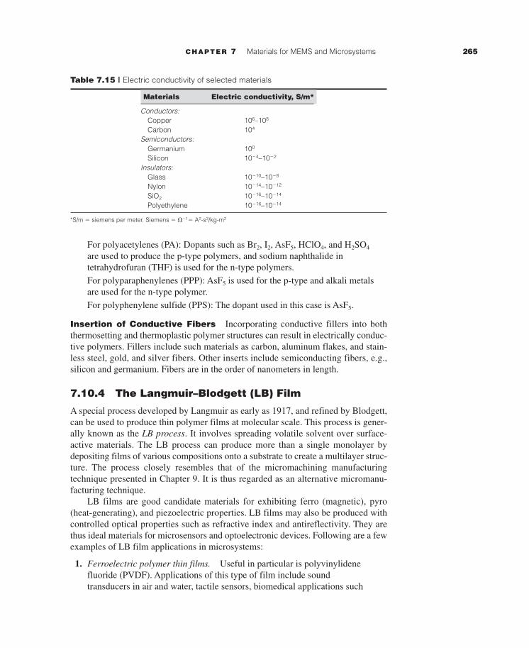
By nature, polymers are poor electric conductors. Table 7.15 shows the electricconductivity of various materials. One will readily see that polymers, represented bypolyethylene, have the lowest electric conductance of all the listed materials.
Polymers can be made electrically conductive by the following three methods:
Pyrolysis A pyropolymer based on phthalonitrile resin can be made electricallyconductive by adding an amine heated above 600°C. The conductivity of the poly-mer produced by this process can be as high as 2.7 � 104 S/m, which is slightly bet-ter than that of carbon.
Doping Doping with the introduction of an inherently conductive polymer struc-ture, such as by incorporating a transition metal atom into the polymer backbone, canresult in electrically conductive polymers. Doping of polymers depends on thedopants and the individual polymer. Following are examples of dopants used in pro-ducing electrically conductive polymers:
hsu93912_ch07.qxd 10/1/2001 12:46 PM Page 264
CHAPTER 7 Materials for MEMS and Microsystems 265
For polyacetylenes (PA): Dopants such as Br2, I2, AsF5, HClO4, and H2SO4
are used to produce the p-type polymers, and sodium naphthalide intetrahydrofuran (THF) is used for the n-type polymers.
For polyparaphenylenes (PPP): AsF5 is used for the p-type and alkali metalsare used for the n-type polymer.
For polyphenylene sulfide (PPS): The dopant used in this case is AsF5.
Insertion of Conductive Fibers Incorporating conductive fillers into boththermosetting and thermoplastic polymer structures can result in electrically conduc-tive polymers. Fillers include such materials as carbon, aluminum flakes, and stain-less steel, gold, and silver fibers. Other inserts include semiconducting fibers, e.g.,silicon and germanium. Fibers are in the order of nanometers in length.
7.10.4 The Langmuir–Blodgett (LB) Film
A special process developed by Langmuir as early as 1917, and refined by Blodgett,can be used to produce thin polymer films at molecular scale. This process is gener-ally known as the LB process. It involves spreading volatile solvent over surface-active materials. The LB process can produce more than a single monolayer bydepositing films of various compositions onto a substrate to create a multilayer struc-ture. The process closely resembles that of the micromachining manufacturingtechnique presented in Chapter 9. It is thus regarded as an alternative micromanu-facturing technique.
LB films are good candidate materials for exhibiting ferro (magnetic), pyro(heat-generating), and piezoelectric properties. LB films may also be produced withcontrolled optical properties such as refractive index and antireflectivity. They arethus ideal materials for microsensors and optoelectronic devices. Following are a fewexamples of LB film applications in microsystems:
1. Ferroelectric polymer thin films. Useful in particular is polyvinylidenefluoride (PVDF). Applications of this type of film include soundtransducers in air and water, tactile sensors, biomedical applications such
Table 7.15 | Electric conductivity of selected materials
Materials Electric conductivity, S/m*
Conductors:Copper 106–108
Carbon 104
Semiconductors:Germanium 100
Silicon 10�4–10�2
Insulators:Glass 10�10–10�8
Nylon 10�14–10�12
SiO2 10�16–10�14
Polyethylene 10�16–10�14
*S/m siemens per meter. Siemens ��1 A2-s3/kg-m2
hsu93912_ch07.qxd 10/1/2001 12:46 PM Page 265
266 MEMS and Microsystems: Design and Manufacture
as tissue-compatible implants, cardiopulmonary sensors, and implantabletransducers and sensors for prosthetics and rehabilitation devices. Thepiezoelectric coefficient of PVDF is given in Table 7.14.
2. Coating materials with controllable optical properties. These are widelyused in broadband optical fibers, which can transmit laser light at differentwavelengths.
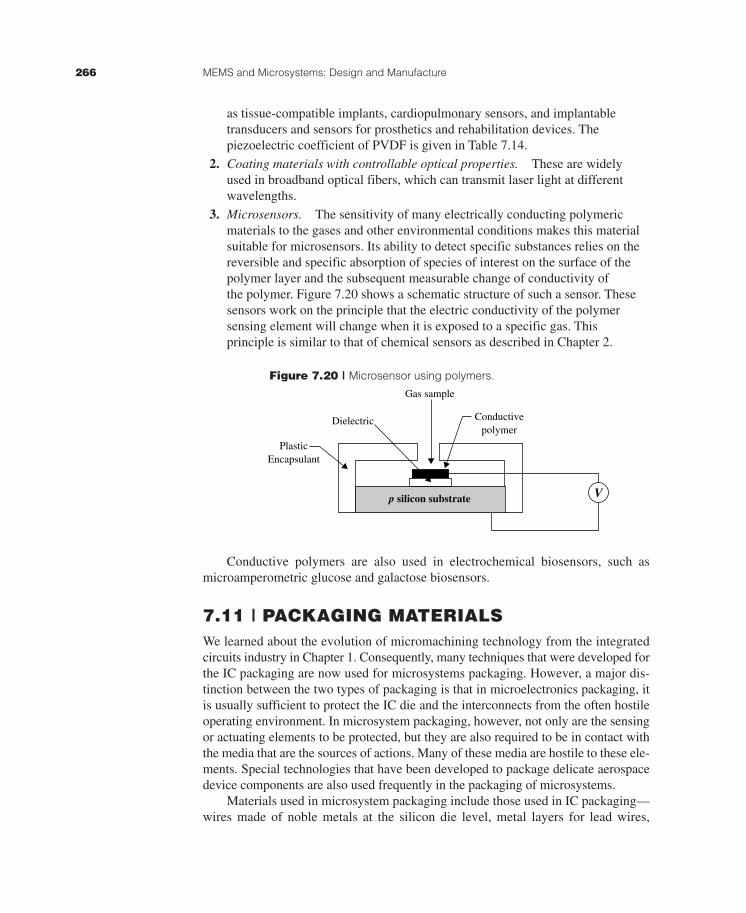
3. Microsensors. The sensitivity of many electrically conducting polymericmaterials to the gases and other environmental conditions makes this materialsuitable for microsensors. Its ability to detect specific substances relies on thereversible and specific absorption of species of interest on the surface of thepolymer layer and the subsequent measurable change of conductivity ofthe polymer. Figure 7.20 shows a schematic structure of such a sensor. Thesesensors work on the principle that the electric conductivity of the polymersensing element will change when it is exposed to a specific gas. Thisprinciple is similar to that of chemical sensors as described in Chapter 2.
Figure 7.20 | Microsensor using polymers.
Conductive polymers are also used in electrochemical biosensors, such asmicroamperometric glucose and galactose biosensors.
7.11 | PACKAGING MATERIALSWe learned about the evolution of micromachining technology from the integratedcircuits industry in Chapter 1. Consequently, many techniques that were developed forthe IC packaging are now used for microsystems packaging. However, a major dis-tinction between the two types of packaging is that in microelectronics packaging, itis usually sufficient to protect the IC die and the interconnects from the often hostileoperating environment. In microsystem packaging, however, not only are the sensingor actuating elements to be protected, but they are also required to be in contact withthe media that are the sources of actions. Many of these media are hostile to these ele-ments. Special technologies that have been developed to package delicate aerospacedevice components are also used frequently in the packaging of microsystems.
Materials used in microsystem packaging include those used in IC packaging—wires made of noble metals at the silicon die level, metal layers for lead wires,
V
Dielectric Conductivepolymer
PlasticEncapsulant
Gas sample
p silicon substrate
hsu93912_ch07.qxd 10/1/2001 12:46 PM Page 266
CHAPTER 7 Materials for MEMS and Microsystems 267
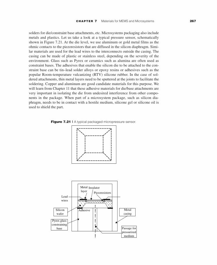
solders for die/constraint base attachments, etc. Microsystems packaging also includemetals and plastics. Let us take a look at a typical pressure sensor, schematicallyshown in Figure 7.21. At the die level, we use aluminum or gold metal films as theohmic contacts to the piezoresistors that are diffused in the silicon diaphragm. Simi-lar materials are used for the lead wires to the interconnects outside the casing. Thecasing can be made of plastic or stainless steel, depending on the severity of theenvironment. Glass such as Pyrex or ceramics such as alumina are often used asconstraint bases. The adhesives that enable the silicon die to be attached to the con-straint base can be tin–lead solder alloys or epoxy resins or adhesives such as thepopular Room-temperature vulcanizing (RTV) silicone rubber. In the case of sol-dered attachments, thin metal layers need to be sputtered at the joints to facilitate thesoldering. Copper and aluminum are good candidate materials for this purpose. Wewill learn from Chapter 11 that these adhesive materials for die/base attachments arevery important in isolating the die from undesired interference from other compo-nents in the package. When part of a microsystem package, such as silicon dia-phragm, needs to be in contact with a hostile medium, silicone gel or silicone oil isused to shield the part.
Figure 7.21 | A typical packaged micropressure sensor.
Leadwires
Metallayer
Metalcasing
Adhesive
Pyrex glassconstraining
base
Siliconwafer
Passage forpressurized
medium
Insulator
Piezoresistors
hsu93912_ch07.qxd 10/1/2001 12:46 PM Page 267
268 MEMS and Microsystems: Design and Manufacture
PROBLEMSPart 1. Multiple Choice
1. A substrate is (1) a sublayer in MEMS, (2) a flat microscopic object, (3) a flatmacroscopic object in microelectronics.
2. A semiconducting material can be made to become an electrically conductingmaterial by (1) applying high electric voltage, (2) applying high current,(3) introducing the right kind of foreign atoms into the semiconductingmaterial.
3. Silicon has a Young’s modulus similar to that of (1) aluminum, (2) stainlesssteel, (3) copper.
4. Silicon has a mass density similar to that of (1) aluminum, (2) stainless steel,(3) copper.
5. The principal reason why silicon is an ideal material for MEMS is (1) itsdimensional stability over a wide range of temperatures, (2) it is lightand strong, (3) it is readily available.
6. Silicon has a coefficient of thermal expansion (1) higher than, (2) lowerthan, (3) about the same as that of silicon dioxide.
7. The 300-mm wafers offer (1) 2, (2) 2.25, (3) 2.5 times more area forsubstrates than that by 200-mm wafers.
8. The length of the lattice of a silicon crystal is (1) 0.543, (2) 0.643,(3) 0.743 nanometer.
9. Miller’s indices are used to designate (1) the length, (2) the plane, (3) thevolume of a face-centered cubic crystal.
10. The (100) plane in a silicon crystal consists of (1) 5, (2) 8, (3) 6 atoms.
11. The (110) plane in a silicon crystal consists of (1) 5, (2) 8, (3) 6 atoms.
12. The (111) plane in a silicon crystal consists of (1) 5, (2) 8, (3) 6 atoms.
13. The growth of silicon crystals is slowest in the (1) �100�, (2) �110�,(3) �111� direction.
14. Silicon conducts heat (1) 50, (2) 150, (3) 200 times faster than silicon oxide.
15. Silicon carbide films are used to protect (1) the underlying substrates, (2) theintegrated circuits, (3) the electric interconnects in a microsystem.
16. Silicon nitride is (1) tougher than, (2) weaker than, (3) about the same assilicon in strength.
17. Pure and single-crystal silicon (1) exists in nature, (2) is grown from specialprocesses, (3) is made by electrolysis.
18. Wafers used in MEMS and microelectronics are (1) the products of a single-crystal silicon boule, (2) are synthesized from silicon compounds, (3) existin nature.
19. MEMS design engineers are advised to adopt (1) any size, (2) a custom-specified size, (3) an industrial standard size of wafer.
20. The total number of atoms in a silicon unit crystal is (1) 18, (2) 16, (3) 14.
hsu93912_ch07.qxd 10/1/2001 12:46 PM Page 268
CHAPTER 7 Materials for MEMS and Microsystems 269
21. The toughest plane for processing in a single silicon crystal is (1) the(100) plane, (2) the (110) plane, (3) the (111) plane.
22. The 54.74° slope in the cavity of a silicon die for a pressure sensor is(1) determined by choice, (2) a result of the crystal’s resistance to etchingin the (111) plane, (3) a result of the crystal’s resistance to etching in the(110) plane.
23. Polysilicon is popular because it can easily be made as a (1) semiconductor,(2) insulator, (3) electrical conductor.
24. Polysilicon films are used in microsystems as (1) dielectric material,(2) substrate material, (3) electrically conducting material.
25. The electrical resistance of silicon piezoresistors varies in (1) all directions,(2) only in the preferred directions, (3) neither of the above applies.
26. It is customary to relate silicon piezoresistance change to (1) deformations,(2) strains, (3) stresses induced in the piezoresistors in MEMS andmicrosystems.
27. There are (1) three, (2) four, (3) six piezoresistive coefficients in siliconpiezoresistors.
28. The single most serious disadvantage of using silicon piezoresistor is (1) thehigh cost of producing such resistors, (2) its strong sensitivity to signaltransduction, (3) its strong sensitivity to temperature.
29. Gallium arsenide has (1) 6, (2) 7, (3) 8 times higher electron mobility thansilicon.
30. Gallium arsenide is chosen over silicon for the use in micro-optical devicesbecause of its (1) optical reflectivity, (2) dimensional stability, (3) high electronmobility.
31. Gallium arsenide is not as popular as silicon in MEMS application because of(1) its higher cost in production, (2) difficulty of mechanical work, (3) lowmechanical strength.
32. Quartz crystals have the shape of (1) a cube, (2) a tetrahedron, (3) a body-centered cube.
33. It is customary to relate the voltage produced by a piezoelectric crystal to the(1) deformations, (2) temperature, (3) stresses induced in the crystal.
34. Application of mechanical deformation to a piezoelectric crystal can result inthe production of (1) electric resistance change, (2) electric current change,(3) electric voltage change in the crystal.
35. Most piezoelectric crystals (1) exist in nature, (2) are made by syntheticprocesses, (3) are made by doping the substrate.
36. A polymer is a material that is made up of many (1) small-size, (2) large-size,(3) long-chain molecules.
37. In general, polymers are (1) electrically conductive, (2) semi electricallyconductive, (3) insulators.
38. Polymers (1) can, (2) cannot, (3) may never be made electrically conductive.
hsu93912_ch07.qxd 10/1/2001 12:46 PM Page 269
270 MEMS and Microsystems: Design and Manufacture
39. The LB process is used to produce (1) thin films, (2) dies, (3) piezoelectricpolymers in MEMS and microsystems.
40. MEMS and microsystem packaging materials are (1) restricted tomicroelectronics packaging materials, (2) just about all engineering materials,(3) semiconducting materials.
Part 2. Computational Problems
1. Estimate the maximum number of silicon dies of size of 2 mm wide � 4 mmlong that can be accommodated in the four standard-sized wafers given inSection 7.4.2. The dies are laid out in parallel on the wafer with 0.25-m gapsbetween dies. Make your observation on the results.
2. Prove that the 300-mm wafers do indeed have 2.25 times larger area forsubstrates than that of 200-mm wafers.
3. Estimate the number of atoms per cubic millimeter and cubic micrometer ofpure silicon.
4. Find the change of electric resistance if a piezoresistor made of p-type siliconreplaces the piezoelectric crystal in Example 7.4. The piezoresistor has a lengthof 4 m.
5. What would be the voltage output of the piezoelectric transducer inExample 7.4 if PVDF polymer films were used instead?
6. Determine the length of lattices that bond the atoms in the three principalplanes of the silicon crystal shown in Figure 7.8.
7. Determine the spacing between atoms in the three planes in a single siliconcrystal as illustrated in Figure 7.10.
8. Determine the angle between the orientation �100� to the (111) plane in asingle silicon crystal cell.
9. For homogeneous and isotropic solids, the relation between the three elasticconstants is E 2(1 � �)G exists. In this relationship, E is the Young’smodulus, � is Poisson’s ratio, and G is the shear modulus of elasticity.Determine the Young’s modulus of silicon in three orientations in Table 7.2using the tabulated values of � and G, and compare the computed results withthose tabulated.
10. Determine the electric voltage required to pump a droplet of ink from the wellin Example 7.5 with a resolution of 600 dpi.
hsu93912_ch07.qxd 10/1/2001 12:46 PM Page 270