Embed Size (px)
Citation preview
Board Level Temperature Cycling Study of Large Array Wafer Level Package
M. S. Kaysar Rahim1, Tiao Zhou1, Xuejun Fan2, and Guy Rupp1 1Maxim Integrated Products
4401 S. Beltwood Pkwy, Dallas, TX 75244 2Department of Mechanical Engineering
Lamar University, Beaumont, TX E-Mail: [email protected]
Abstract
The demand for Wafer Level Packages (WLP) has increased significantly due to its smaller package size and lower cost. However, board level reliability of WLP is still a major concern. This study investigates the board level temperature cycle reliability of three very different wafer level package configurations. Comprehensive studies are carried out through temperature cycle test, failure analysis, and finite element modeling. To assess the wafer level package capability and technology limit, the following parameters are considered: WLP structure, array size, ball locations, ball pitch, and temperature cycle profile.
Daisy-chain chips are used for this study. Extensive failure analysis was carried out to confirm failure mechanism and quantify the mechanical degradation among different solder joints due to temperature cycle stressing. It is suggested that the primary failure mechanism is solder fatigue. The crack is in bulk solder at package side. The cracks initiate from both sides of the solder joint. The cracks propagate from edge toward the center of the solder ball. The corner balls are most susceptible to solder joint failures. Based on test data, making corner balls electrically not connected improves the WLP reliability by 30%.
It is concluded that WLP structure A has superior solder joint reliability compared to B and C. For a given ball array size, smaller pitch gives better solder joint life. The solder joint fatigue life is approximately 1.2 times longer for 2 cycle per hour (cph) conditions than 1 cph temperature cycling condition. Introduction
WLP provides a great solution to meet the demand of an emerging market for smaller, thinner, and faster electronic products. Because of its lower cost and higher performance, WLP takes a strong position in hand held and mobile electronic systems. Meanwhile thermo-mechanical reliability of WLP is still a major concern for higher I/Os and larger die. One of the key reliability tests is board level temperature cycle test.
There are very few literature published on WLP temperature cycle test [1-4]. Driel et al. [1] published results on 1st and 2nd level reliability of WLP using combined experimental and virtual prototyping (thermal, mechanical and thermo-mechanical) techniques. Novel wafer-level chip scale packages (WLCSP) with a stress buffer layer and bubble-like plate were proposed to improve the solder joint fatigue life by Lee et al. [2]. Zbrzezny el at. [3] studied the board level reliability through thermal cycle, drop and cyclic
bend tests for WLPs from different vendors. A full set of board level testing was performed by Rinne et al. [4] on WLPs with an aim at choosing an appropriate material for a dielectric layer and also at optimizing their thickness. Fan et al. [5] performed a study on a variety of WLP technologies, with the emphasis on the fundamental principles of WLP solder joint reliability and improvement by introducing various designs. The effects design parameters of WLCSP, including solder joint layout, solder volume, pad diameter, ratio, and orientation of the elliptical pad were studied respectively by Liu, Vandevelde and Keser et al. [6-8]. Lau et al. [9] explored the effects of the thickness of a built-up printed circuit board (PCB) on the solder joint reliability of a WLCSP. Several studies were conducted to investigate effects of chip thickness and solder material ([10] and [11]). The enhancement of solder joint reliability also studied by placing large dummy balls at the outermost corners of the solder joint array [12]. Kazama et al. [13] employed the finite element analysis (FEA) to optimize the built-in stress- relaxation layer for reducing the strain of the solder bumps. Gao et al. [14] reported a novel design to enhance the board level reliability by incorporating a compliant polymer layer under the UBM.
Since WLP technology eliminates underfill, the solder joint becomes the weakest link in the WLP board level assemblies. Solder joint fatigue is common failure mechanism during temperature cycle test. The primary mechanism for solder joint fatigue is the mismatch in the coefficients of thermal expansion (CTE) of the various packaging materials. The CTE mismatches become worse with the increase of DNP, so the solder fatigue is more severe for larger array WLP. Other WLP failure mechanisms accelerated by temperature cycling include die cracking, package cracking, PCB via crack, PCB trace crack, and PCB pad lifting. To improve the board level reliability of large array WLP, detailed understanding of different design is needed. In this work, board level temperature cycle reliability of three very different wafer level package configurations are studied through temperature cycling test, failure analysis, and thermomechanical modeling.
Daisy-chain chips are used to study the reliability WLP in this study. Extensive failure analysis was carried out to confirm failure mechanism and quantify the mechanical degradation among different solder joints due to temperature cycle stressing. Eight potential failure mechanisms are investigated in this study. In order to quantify the failure rate of corner solder joints in comparison to other solder joints, two daisy chain loops are constructed at the board level for
978-1-4244-4476-2/09/$25.00 ©2009 IEEE 898 2009 Electronic Components and Technology Conference
every daisy chain test chip. Failure rates for both groups are presented based on experimental data. This is the first time the effects of solder joint locations on the WLP reliability were verified experimentally. Fatigue life as functions of array size and pitch is also presented. The effects of array size and ball pitch on the WLP reliability are also investigated. Wafer Level Packages Parameters
To assess the wafer level package capability and technology limit, the following parameters are considered in the study:
1. Different WLP structures A, B, and C 2. Ball pitches of 0.5 and 0.4 mm. 3. Temperature cycling rate of 1 and 2 cycles per hour
(cph) 4. Array sizes of 12x12 and 10x10 5. Corner ball being functional or no electrical
connection. Fully populated arrays are considered in this study. They
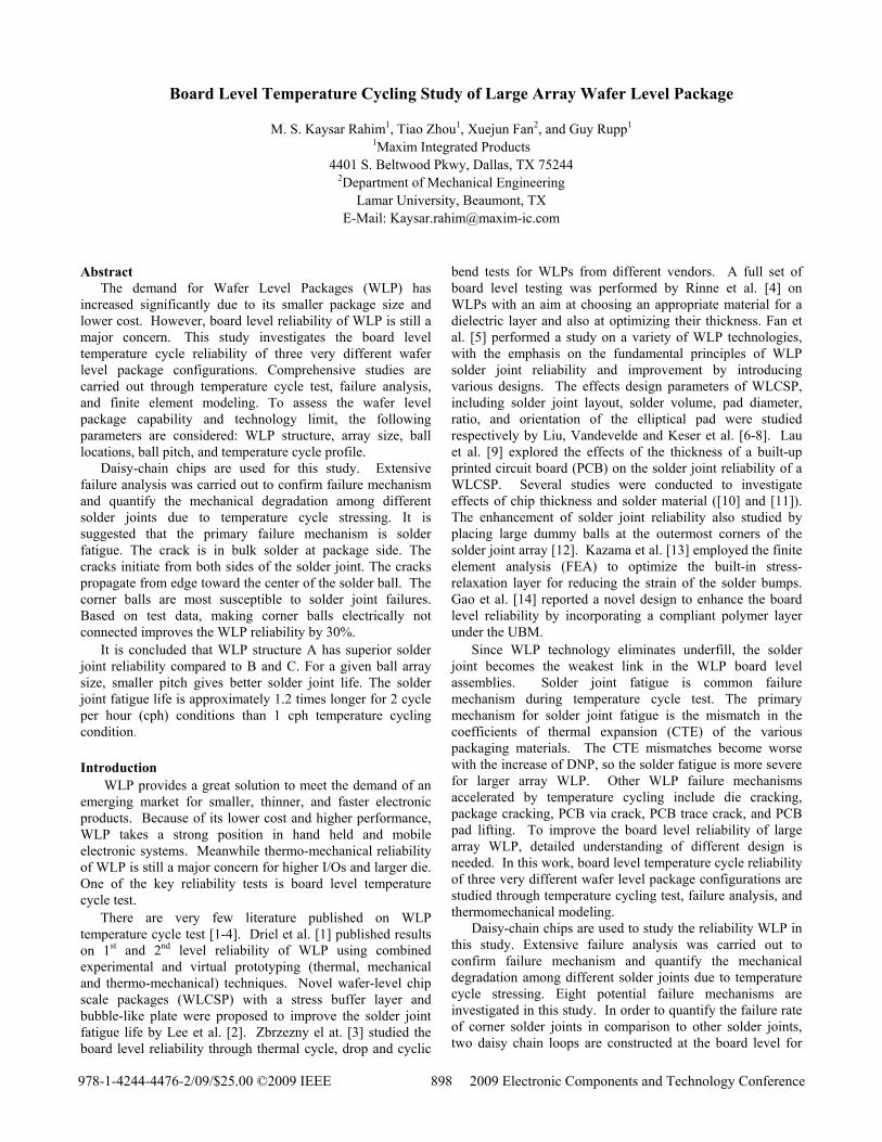
are illustrated in Figure 1. The solder balls included in the corner ball loop are shown in Figure 2. The temperature range considered is -45oC to +125oC. The failure criterion defined by IPC-SM-785 is used in this study. 12x12 array WLP-C is considered as baseline for comparison purpose. Fatigue lives of different options are normalized with respect to this case.
Figure 1. 10 x 10 and 12 x 12 Array
Figure 2. Solder Balls Included in Corner and Center
daisy Chain Loops
Experimental Data WLP Structures A, B and C:
The fatigue lives of the three structures are listed in Table 1. It is observed that the WLP-A has significantly longer fatigue life than WLP-B and WLP-C. WLP-B has the worst fatigue life. WLP design and material selection plays a significant role in board level reliability.
Table 1. Normalized Characteristic Life for Different
WLP Structures.
WLP Type WLP - A WLP - B WLP - C
Characteristic Life 1.6 0.8 1
Array Size: A comparison of failure data for 10 x 10 and 12 x 12 array
sizes for WLP- C is shown in Table 2. It is observed that WLP-C, 10 x 10 array has 20% longer fatigue life than 12 x 12 array. In this case the ratio of WLP size between 12x12 and 10x10 array is 1.2. It appears that the fatigue life is inversely proportional to the package size.
Table2. Normalized Characteristic Life for 12x12 and 10x10 Array WLP. Array Size 12x12 10x10Characteristic life 1 1.2
Corner Balls:
A comparison of failure data for corner and non corner balls (Figure 2) is shown in Table 3. It is observed that the non-corner balls have 30% longer fatigue life than corner daisy chain loop. In other words, making the corner balls electrically not connected will improve the fatigue life by 40%. Comparison of results in Tables 2 and 3 suggests that the solder joint reliability for a 12x12 array WLP with corner balls electrically connected is better than a 10x10 full array WLP.
Table 3. Normalized Characteristic Life for
Corner and Non-Corner solder balls
Solder Ball Groups Corner Non-cornerCharacteristic Life 1 1.3
WLP Ball Pitch:
12x12 array WLPs with 0.5 and 0.4 mm pitches are tested. WLP fatigue lives are compared against each other (Table 4). It is observed that 0.4 mm pitch has 30% longer fatigue life than 0.5 mm for a given ball count.
899 2009 Electronic Components and Technology Conference
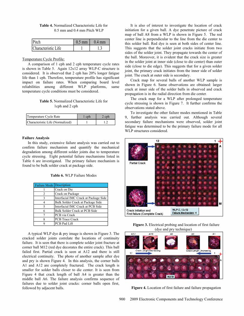
Table 4. Normalized Characteristic Life for 0.5 mm and 0.4 mm Pitch WLP
Pitch 0.5 mm 0.4 mmCharacteristic Life 1 1.3
Temperature Cycle Profile:
A comparison of 1 cph and 2 cph temperature cycle rates is shown in Table 5. Again 12x12 array WLP-C structure is considered. It is observed that 2 cph has 20% longer fatigue life than 1 cph. Therefore, temperature profile has significant impact on failure rates. When comparing board level reliabilities among different WLP platforms, same temperature cycle conditions must be considered.
Table 5. Normalized Characteristic Life for 1cph and 2 cph
Temperature Cycle Rate 1 cph 2 cph
Characteristic Life (Normalized) 1 1.2
Failure Analysis
In this study, extensive failure analysis was carried out to confirm failure mechanism and quantify the mechanical degradation among different solder joints due to temperature cycle stressing. Eight potential failure mechanisms listed in Table 6 are investigated. The primary failure mechanism is found to be bulk solder crack at package side.
Table 6. WLP Failure Modes
Failure Mode
123456789
PCB Trace CrackPCB Pad Lift
Bulk Solder Crack at Package SideInterfacial IMC Crack at PCB SideBulk Solder Crack at PCB SidePCB via Crack
DescriptionCrack on DieCrack on PackageInterfacial IMC Crack at Package Side
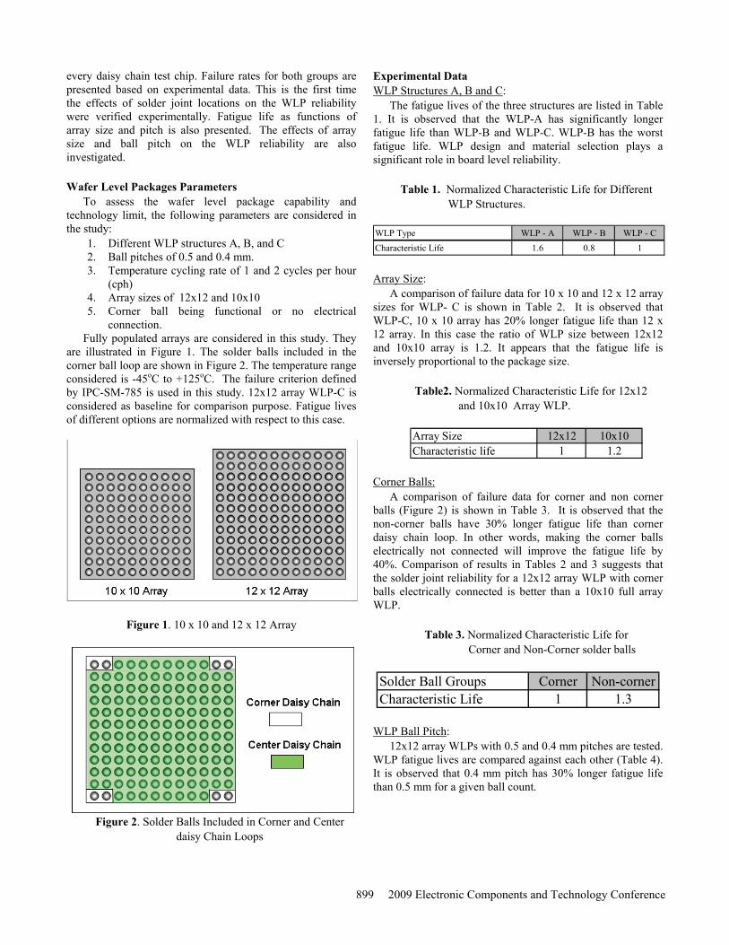
A typical WLP dye & pry image is shown in Figure 3. The cracked solder joints correlate the locations of continuity failure. It is seen that there is complete solder joint fracture at corner ball M12 (red dye decorates the entire crack). This ball failed first. Partial crack is seen at A12 and there is still electrical continuity. The photo of another sample after dye and pry is shown Figure 4. In this analysis, the corner balls A1 and A12 are completely fractured. The crack length is smaller for solder balls closer to die center. It is seen from Figure 4 that crack length of ball A4 is greater than the middle ball A6. The failure analysis confirms sequence of failures due to solder joint cracks: corner balls open first, followed by adjacent balls.
It is also of interest to investigate the location of crack initiation for a given ball. A dye penetrate picture of crack map of ball A8 from a WLP is shown in Figure 5. The red center line is perpendicular to the line from the die center to this solder ball. Red dye is seen at both sides of center line. This suggests that the solder joint cracks initiate from two sides of the solder joint. They propagate towards the center of the ball. Moreover, it is evident that the crack size is greater in the solder joint at inner side (close to die center) than outer side (close to die edge). This suggests that for a given solder joint, the primary crack initiates from the inner side of solder joint. The crack at outer side is secondary.
Crack map for several balls of another WLP sample is shown in Figure 6. Same observations are obtained: larger crack at inner side of the solder balls in observed and crack propagation is in the radial direction from die center.
The crack map for a WLP after prolonged temperature cycle stressing is shown in Figure 7. It further confirms the observations stated above.
To investigate the other failure modes mentioned in Table 9, further analysis was carried out. Although several secondary failure mechanisms were observed, solder joint fatigue was determined to be the primary failure mode for all WLP structures considered.
Figure 3. Electrical probing and location of first failure (dye and pry technique)
Figure 4. Location of first failure and failure propagation
900 2009 Electronic Components and Technology Conference
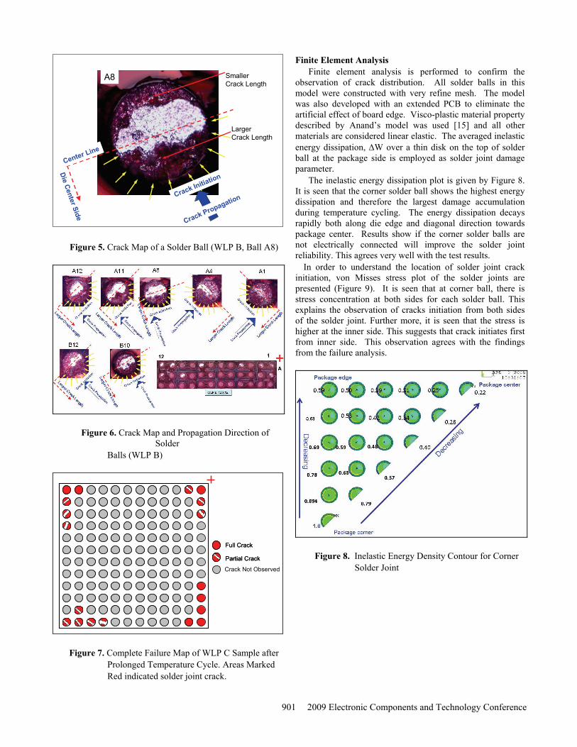
A8
Center Line
Crack Propagation
Die C
enter S
ide
Larger Crack Length
Smaller Crack Length
Crack Initiation
Figure 5. Crack Map of a Solder Ball (WLP B, Ball A8)
Figure 6. Crack Map and Propagation Direction of Solder
Balls (WLP B)
Full Crack
Partial Crack
Full Crack
Partial Crack
Crack Not Observed
Figure 7. Complete Failure Map of WLP C Sample after Prolonged Temperature Cycle. Areas Marked Red indicated solder joint crack.
Finite Element Analysis Finite element analysis is performed to confirm the
observation of crack distribution. All solder balls in this model were constructed with very refine mesh. The model was also developed with an extended PCB to eliminate the artificial effect of board edge. Visco-plastic material property described by Anand’s model was used [15] and all other materials are considered linear elastic. The averaged inelastic energy dissipation, W over a thin disk on the top of solder ball at the package side is employed as solder joint damage parameter.
The inelastic energy dissipation plot is given by Figure 8. It is seen that the corner solder ball shows the highest energy dissipation and therefore the largest damage accumulation during temperature cycling. The energy dissipation decays rapidly both along die edge and diagonal direction towards package center. Results show if the corner solder balls are not electrically connected will improve the solder joint reliability. This agrees very well with the test results.
In order to understand the location of solder joint crack initiation, von Misses stress plot of the solder joints are presented (Figure 9). It is seen that at corner ball, there is stress concentration at both sides for each solder ball. This explains the observation of cracks initiation from both sides of the solder joint. Further more, it is seen that the stress is higher at the inner side. This suggests that crack initiates first from inner side. This observation agrees with the findings from the failure analysis.
Figure 8. Inelastic Energy Density Contour for Corner Solder Joint
901 2009 Electronic Components and Technology Conference
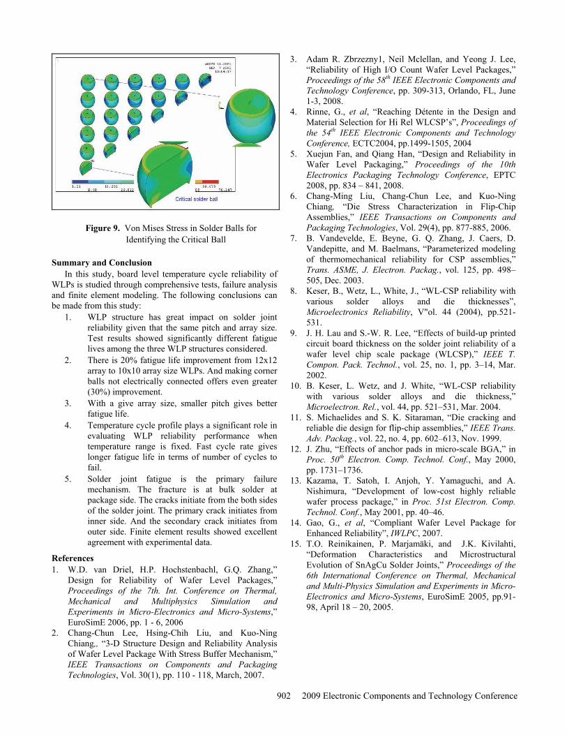
Figure 9. Von Mises Stress in Solder Balls for Identifying the Critical Ball
Summary and Conclusion
In this study, board level temperature cycle reliability of WLPs is studied through comprehensive tests, failure analysis and finite element modeling. The following conclusions can be made from this study:
1. WLP structure has great impact on solder joint reliability given that the same pitch and array size. Test results showed significantly different fatigue lives among the three WLP structures considered.
2. There is 20% fatigue life improvement from 12x12 array to 10x10 array size WLPs. And making corner balls not electrically connected offers even greater (30%) improvement.
3. With a give array size, smaller pitch gives better fatigue life.
4. Temperature cycle profile plays a significant role in evaluating WLP reliability performance when temperature range is fixed. Fast cycle rate gives longer fatigue life in terms of number of cycles to fail.
5. Solder joint fatigue is the primary failure mechanism. The fracture is at bulk solder at package side. The cracks initiate from the both sides of the solder joint. The primary crack initiates from inner side. And the secondary crack initiates from outer side. Finite element results showed excellent agreement with experimental data.
References 1. W.D. van Driel, H.P. Hochstenbachl, G.Q. Zhang,”
Design for Reliability of Wafer Level Packages,” Proceedings of the 7th. Int. Conference on Thermal, Mechanical and Multiphysics Simulation and Experiments in Micro-Electronics and Micro-Systems,” EuroSimE 2006, pp. 1 - 6, 2006
2. Chang-Chun Lee, Hsing-Chih Liu, and Kuo-Ning Chiang,, “3-D Structure Design and Reliability Analysis of Wafer Level Package With Stress Buffer Mechanism,” IEEE Transactions on Components and Packaging Technologies, Vol. 30(1), pp. 110 - 118, March, 2007.
3. Adam R. Zbrzezny1, Neil Mclellan, and Yeong J. Lee, “Reliability of High I/O Count Wafer Level Packages,” Proceedings of the 58th IEEE Electronic Components and Technology Conference, pp. 309-313, Orlando, FL, June 1-3, 2008.
4. Rinne, G., et al, “Reaching Détente in the Design and Material Selection for Hi Rel WLCSP’s”, Proceedings of the 54th IEEE Electronic Components and Technology Conference, ECTC2004, pp.1499-1505, 2004
5. Xuejun Fan, and Qiang Han, “Design and Reliability in Wafer Level Packaging,” Proceedings of the 10th Electronics Packaging Technology Conference, EPTC 2008, pp. 834 – 841, 2008.
6. Chang-Ming Liu, Chang-Chun Lee, and Kuo-Ning Chiang, “Die Stress Characterization in Flip-Chip Assemblies,” IEEE Transactions on Components and Packaging Technologies, Vol. 29(4), pp. 877-885, 2006.
7. B. Vandevelde, E. Beyne, G. Q. Zhang, J. Caers, D. Vandepitte, and M. Baelmans, “Parameterized modeling of thermomechanical reliability for CSP assemblies,” Trans. ASME, J. Electron. Packag., vol. 125, pp. 498–505, Dec. 2003.
8. Keser, B., Wetz, L., White, J., “WL-CSP reliability with various solder alloys and die thicknesses”, Microelectronics Reliability, V"ol. 44 (2004), pp.521-531.
9. J. H. Lau and S.-W. R. Lee, “Effects of build-up printed circuit board thickness on the solder joint reliability of a wafer level chip scale package (WLCSP),” IEEE T. Compon. Pack. Technol., vol. 25, no. 1, pp. 3–14, Mar. 2002.
10. B. Keser, L. Wetz, and J. White, “WL-CSP reliability with various solder alloys and die thickness,” Microelectron. Rel., vol. 44, pp. 521–531, Mar. 2004.
11. S. Michaelides and S. K. Sitaraman, “Die cracking and reliable die design for flip-chip assemblies,” IEEE Trans. Adv. Packag., vol. 22, no. 4, pp. 602–613, Nov. 1999.
12. J. Zhu, “Effects of anchor pads in micro-scale BGA,” in Proc. 50th Electron. Comp. Technol. Conf., May 2000, pp. 1731–1736.
13. Kazama, T. Satoh, I. Anjoh, Y. Yamaguchi, and A. Nishimura, “Development of low-cost highly reliable wafer process package,” in Proc. 51st Electron. Comp. Technol. Conf., May 2001, pp. 40–46.
14. Gao, G., et al, “Compliant Wafer Level Package for Enhanced Reliability”, IWLPC, 2007.
15. T.O. Reinikainen, P. Marjamäki, and J.K. Kivilahti, “Deformation Characteristics and Microstructural Evolution of SnAgCu Solder Joints,” Proceedings of the 6th International Conference on Thermal, Mechanical and Multi-Physics Simulation and Experiments in Micro-Electronics and Micro-Systems, EuroSimE 2005, pp.91-98, April 18 – 20, 2005.
902 2009 Electronic Components and Technology Conference