Embed Size (px)
Citation preview
Blackfin and the Blackfin logo are registered trademarks of Analog Devices, Inc.
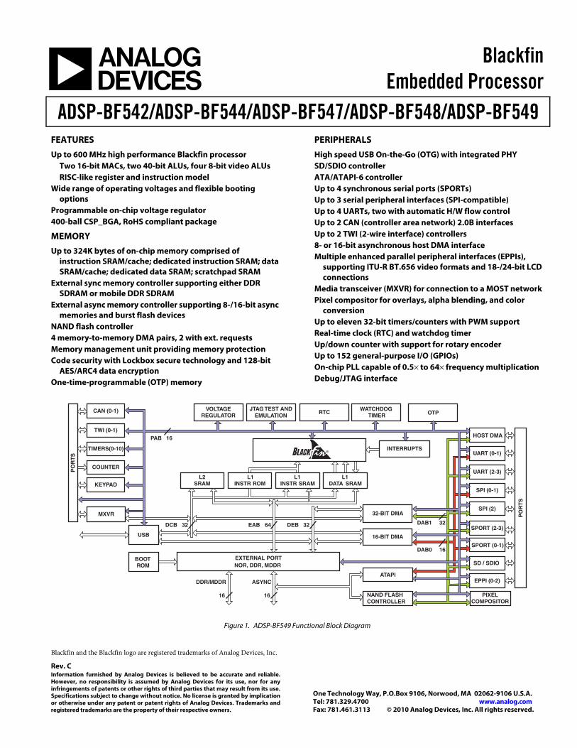
BlackfinEmbedded Processor
ADSP-BF542/ADSP-BF544/ADSP-BF547/ADSP-BF548/ADSP-BF549
Rev. CInformation furnished by Analog Devices is believed to be accurate and reliable.However, no responsibility is assumed by Analog Devices for its use, nor for anyinfringements of patents or other rights of third parties that may result from its use.Specifications subject to change without notice. No license is granted by implicationor otherwise under any patent or patent rights of Analog Devices. Trademarks andregistered trademarks are the property of their respective owners.
One Technology Way, P.O.Box 9106, Norwood, MA 02062-9106 U.S.A.Tel: 781.329.4700 www.analog.comFax: 781.461.3113 © 2010 Analog Devices, Inc. All rights reserved.
FEATURESUp to 600 MHz high performance Blackfin processor
Two 16-bit MACs, two 40-bit ALUs, four 8-bit video ALUsRISC-like register and instruction model
Wide range of operating voltages and flexible booting options
Programmable on-chip voltage regulator400-ball CSP_BGA, RoHS compliant package
MEMORYUp to 324K bytes of on-chip memory comprised of
instruction SRAM/cache; dedicated instruction SRAM; data SRAM/cache; dedicated data SRAM; scratchpad SRAM
External sync memory controller supporting either DDR SDRAM or mobile DDR SDRAM
External async memory controller supporting 8-/16-bit async memories and burst flash devices
NAND flash controller4 memory-to-memory DMA pairs, 2 with ext. requestsMemory management unit providing memory protectionCode security with Lockbox secure technology and 128-bit
AES/ARC4 data encryptionOne-time-programmable (OTP) memory
PERIPHERALSHigh speed USB On-the-Go (OTG) with integrated PHYSD/SDIO controllerATA/ATAPI-6 controllerUp to 4 synchronous serial ports (SPORTs)Up to 3 serial peripheral interfaces (SPI-compatible)Up to 4 UARTs, two with automatic H/W flow control Up to 2 CAN (controller area network) 2.0B interfacesUp to 2 TWI (2-wire interface) controllers8- or 16-bit asynchronous host DMA interfaceMultiple enhanced parallel peripheral interfaces (EPPIs),
supporting ITU-R BT.656 video formats and 18-/24-bit LCD connections
Media transceiver (MXVR) for connection to a MOST networkPixel compositor for overlays, alpha blending, and color
conversionUp to eleven 32-bit timers/counters with PWM supportReal-time clock (RTC) and watchdog timerUp/down counter with support for rotary encoder Up to 152 general-purpose I/O (GPIOs) On-chip PLL capable of 0.5× to 64× frequency multiplicationDebug/JTAG interface
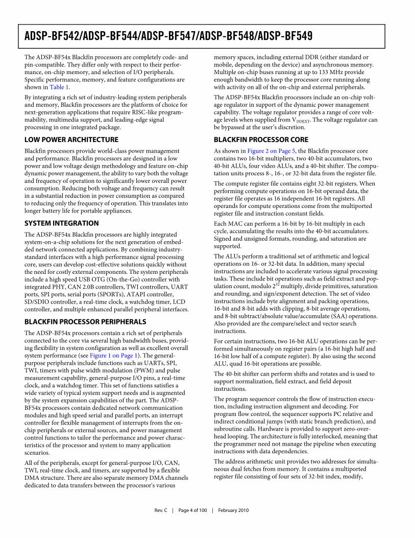
Figure 1. ADSP-BF549 Functional Block Diagram
CAN (0-1)
TWI (0-1)
TIMERS(0-10)
KEYPAD
COUNTER
RTC
HOST DMA
JTAG TEST ANDEMULATION
UART (2-3)
EXTERNAL PORTNOR, DDR, MDDR
SPI (2)
SPORT (0-1)
SD / SDIO
WATCHDOGTIMER
BOOTROM
32
16
PIXELCOMPOSITOR
VOLTAGEREGULATOR
EPPI (0-2)
SPORT (2-3)
SPI (0-1)
UART (0-1)
PO
RT
S
PAB
USB 16-BIT DMA
32-BIT DMA
INTERRUPTS
L2SRAM
L1INSTR ROM
L1INSTR SRAM
L1DATA SRAM
DAB1
DAB0
PO
RT
S
OTP
16 16
DDR/MDDR ASYNC
16
NAND FLASHCONTROLLER
ATAPI
MXVR
DCB 32 EAB 64 DEB 32
B
Rev. C | Page 2 of 100 | February 2010
ADSP-BF542/ADSP-BF544/ADSP-BF547/ADSP-BF548/ADSP-BF549
TABLE OF CONTENTSGeneral Description . . . . . . . . . . . . . . . . . . . . . . . . . . . . . . . . . . . . . . . . . . . . . . . . . 3
Low Power Architecture . . . . . . . . . . . . . . . . . . . . . . . . . . . . . . . . . . . . . . . . . 4System Integration . . . . . . . . . . . . . . . . . . . . . . . . . . . . . . . . . . . . . . . . . . . . . . . . 4Blackfin Processor Peripherals . . . . . . . . . . . . . . . . . . . . . . . . . . . . . . . . . 4Blackfin Processor Core . . . . . . . . . . . . . . . . . . . . . . . . . . . . . . . . . . . . . . . . . . 4Memory Architecture . . . . . . . . . . . . . . . . . . . . . . . . . . . . . . . . . . . . . . . . . . . . 6DMA Controllers . . . . . . . . . . . . . . . . . . . . . . . . . . . . . . . . . . . . . . . . . . . . . . . . 10Real-Time Clock . . . . . . . . . . . . . . . . . . . . . . . . . . . . . . . . . . . . . . . . . . . . . . . . . 11Watchdog Timer . . . . . . . . . . . . . . . . . . . . . . . . . . . . . . . . . . . . . . . . . . . . . . . . 12Timers . . . . . . . . . . . . . . . . . . . . . . . . . . . . . . . . . . . . . . . . . . . . . . . . . . . . . . . . . . . . . 12Up/Down Counter and Thumbwheel Interface . . . . . . . . . . 12Serial Ports (SPORTs) . . . . . . . . . . . . . . . . . . . . . . . . . . . . . . . . . . . . . . . . . . 12Serial Peripheral Interface (SPI) Ports . . . . . . . . . . . . . . . . . . . . . . 13UART Ports (UARTs) . . . . . . . . . . . . . . . . . . . . . . . . . . . . . . . . . . . . . . . . . . 13Controller Area Network (CAN) . . . . . . . . . . . . . . . . . . . . . . . . . . . . 13TWI Controller Interface . . . . . . . . . . . . . . . . . . . . . . . . . . . . . . . . . . . . . . 14Ports . . . . . . . . . . . . . . . . . . . . . . . . . . . . . . . . . . . . . . . . . . . . . . . . . . . . . . . . . . . . . . . . 14Pixel Compositor (PIXC) . . . . . . . . . . . . . . . . . . . . . . . . . . . . . . . . . . . . . . 14Enhanced Parallel Peripheral Interface (EPPI) . . . . . . . . . . . 14USB On-the-Go Dual-Role Device Controller . . . . . . . . . . . . 15ATA/ATAPI-6 Interface . . . . . . . . . . . . . . . . . . . . . . . . . . . . . . . . . . . . . . . 15Keypad Interface . . . . . . . . . . . . . . . . . . . . . . . . . . . . . . . . . . . . . . . . . . . . . . . . . 15Secure Digital (SD)/SDIO Controller . . . . . . . . . . . . . . . . . . . . . . . 16Code Security . . . . . . . . . . . . . . . . . . . . . . . . . . . . . . . . . . . . . . . . . . . . . . . . . . . . 16Media Transceiver MAC Layer (MXVR) . . . . . . . . . . . . . . . . . . 16Dynamic Power Management . . . . . . . . . . . . . . . . . . . . . . . . . . . . . . . . 16Voltage Regulation . . . . . . . . . . . . . . . . . . . . . . . . . . . . . . . . . . . . . . . . . . . . . . 18Clock Signals . . . . . . . . . . . . . . . . . . . . . . . . . . . . . . . . . . . . . . . . . . . . . . . . . . . . . 18
Booting Modes . . . . . . . . . . . . . . . . . . . . . . . . . . . . . . . . . . . . . . . . . . . . . . . . . . . 19Instruction Set Description . . . . . . . . . . . . . . . . . . . . . . . . . . . . . . . . . . . . 22Development Tools . . . . . . . . . . . . . . . . . . . . . . . . . . . . . . . . . . . . . . . . . . . . . . 23
EZ-KIT Lite Evaluation Board . . . . . . . . . . . . . . . . . . . . . . . . . . . . . 23Designing an Emulator-Compatible Processor Board . . . 23MXVR Board Layout Guidelines . . . . . . . . . . . . . . . . . . . . . . . . . . . . . 23Related Documents . . . . . . . . . . . . . . . . . . . . . . . . . . . . . . . . . . . . . . . . . . . . . . 24Lockbox Secure Technology Disclaimer . . . . . . . . . . . . . . . . . . . . 24
Pin Descriptions . . . . . . . . . . . . . . . . . . . . . . . . . . . . . . . . . . . . . . . . . . . . . . . . . . . . 25Specifications . . . . . . . . . . . . . . . . . . . . . . . . . . . . . . . . . . . . . . . . . . . . . . . . . . . . . . . . 34
Operating Conditions . . . . . . . . . . . . . . . . . . . . . . . . . . . . . . . . . . . . . . . . . . . 34Electrical Characteristics . . . . . . . . . . . . . . . . . . . . . . . . . . . . . . . . . . . . . . . 36Absolute Maximum Ratings . . . . . . . . . . . . . . . . . . . . . . . . . . . . . . . . . . . 40ESD Sensitivity . . . . . . . . . . . . . . . . . . . . . . . . . . . . . . . . . . . . . . . . . . . . . . . . . . . 41Package Information . . . . . . . . . . . . . . . . . . . . . . . . . . . . . . . . . . . . . . . . . . . . 41Timing Specifications . . . . . . . . . . . . . . . . . . . . . . . . . . . . . . . . . . . . . . . . . . . 42Output Drive Currents . . . . . . . . . . . . . . . . . . . . . . . . . . . . . . . . . . . . . . . . . 86Test Conditions . . . . . . . . . . . . . . . . . . . . . . . . . . . . . . . . . . . . . . . . . . . . . . . . . . 88Capacitive Loading . . . . . . . . . . . . . . . . . . . . . . . . . . . . . . . . . . . . . . . . . . . . . . 88Typical Rise and Fall Times . . . . . . . . . . . . . . . . . . . . . . . . . . . . . . . . . . . 89Thermal Characteristics . . . . . . . . . . . . . . . . . . . . . . . . . . . . . . . . . . . . . . . . 91
400-Ball CSP_BGA Package . . . . . . . . . . . . . . . . . . . . . . . . . . . . . . . . . . . . . . 92Outline Dimensions . . . . . . . . . . . . . . . . . . . . . . . . . . . . . . . . . . . . . . . . . . . . . . . . 98
Surface-Mount Design . . . . . . . . . . . . . . . . . . . . . . . . . . . . . . . . . . . . . . . . . . 98Automotive Products . . . . . . . . . . . . . . . . . . . . . . . . . . . . . . . . . . . . . . . . . . . . . . 99Ordering Guide . . . . . . . . . . . . . . . . . . . . . . . . . . . . . . . . . . . . . . . . . . . . . . . . . . . 100
REVISION HISTORY2/10—Rev. B to Rev. C Added VIHTWI and VILTWI data to Operating Conditions ...... 34Added IOH/IOL per pin group data to Absolute Maximum Ratings .................................................... 40Added Table 23 (Total Current Pin Groups) ........................ 40Revised all timing diagrams for clarity/consistency in Timing Specifications . . . . . . . . . . . . . . . . . . . . . . . . . . . . . . . . . . . . . . . . . . . . . . . . . . . . . . . . 42Updated specifications (reference PCN 09_0173) in the Clock and Reset Timing section to accurately describe processor cold-startup/reset timing.. . . . . . . . . . . . . . . . . . . . . . . . . . . . . . . . . . . . . . . . . . . . . . . . . 42Added tSUDTE and tSUDRE data to Table 41 (Serial Ports—External Clock) . . . . . . . . . . . . . . . . . . . . . . . . . . . . . . . . . . . . . . . . . . . . . . . . . . . . . . . . . . . . . . . . . . 61
Added tSCLKIW and tSCLK data to Table 42 (Serial Ports—Internal Clock) . . . . . . . . . . . . . . . . . . . . . . . . . . . . . . . . . . . . . . . . . . . . . . . . . . . . . . . . . . . . . . . . . .61 Added Figure 34 (Serial Port Start-Up with External Clock and Frame Sync) and Figure 36 (Serial Ports—Enable and Three-State) ............................................................................................ 62 To view product/process change notifications (PCNs) related to this data sheet revision, please visit the processor's product page on the www.analog.com website and use the View PCN link.
ADSP-BF542/ADSP-BF544/ADSP-BF547/ADSP-BF548/ADSP-BF549
Rev. C | Page 3 of 100 | February 2010
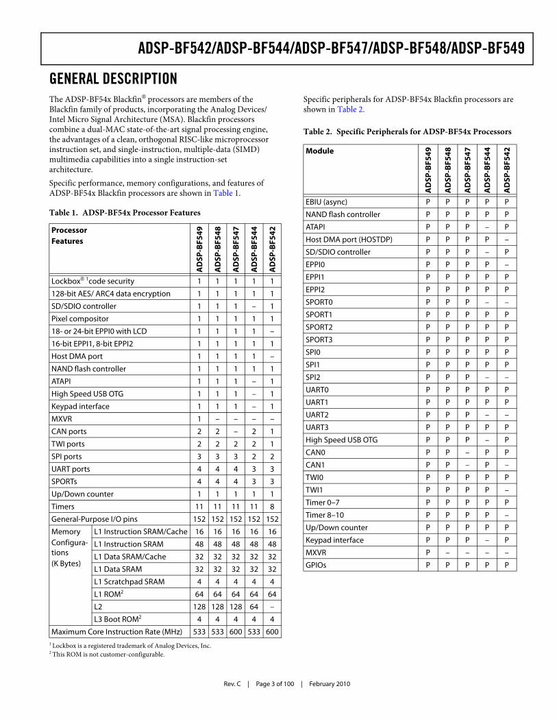
GENERAL DESCRIPTIONThe ADSP-BF54x Blackfin® processors are members of the Blackfin family of products, incorporating the Analog Devices/Intel Micro Signal Architecture (MSA). Blackfin processors combine a dual-MAC state-of-the-art signal processing engine, the advantages of a clean, orthogonal RISC-like microprocessor instruction set, and single-instruction, multiple-data (SIMD) multimedia capabilities into a single instruction-set architecture.Specific performance, memory configurations, and features ofADSP-BF54x Blackfin processors are shown in Table 1.
Specific peripherals for ADSP-BF54x Blackfin processors are shown in Table 2.
Table 1. ADSP-BF54x Processor Features
Processor Features
AD
SP-B
F549
AD
SP-B
F548
AD
SP-B
F547
AD
SP-B
F544
AD
SP-B
F542
Lockbox® 1code security
1 Lockbox is a registered trademark of Analog Devices, Inc.
1 1 1 1 1
128-bit AES/ ARC4 data encryption 1 1 1 1 1
SD/SDIO controller 1 1 1 – 1
Pixel compositor 1 1 1 1 1
18- or 24-bit EPPI0 with LCD 1 1 1 1 –
16-bit EPPI1, 8-bit EPPI2 1 1 1 1 1
Host DMA port 1 1 1 1 –
NAND flash controller 1 1 1 1 1
ATAPI 1 1 1 – 1
High Speed USB OTG 1 1 1 – 1
Keypad interface 1 1 1 – 1
MXVR 1 – – – –
CAN ports 2 2 – 2 1
TWI ports 2 2 2 2 1
SPI ports 3 3 3 2 2
UART ports 4 4 4 3 3
SPORTs 4 4 4 3 3
Up/Down counter 1 1 1 1 1
Timers 11 11 11 11 8
General-Purpose I/O pins 152 152 152 152 152
MemoryConfigura-tions(K Bytes)
L1 Instruction SRAM/Cache 16 16 16 16 16
L1 Instruction SRAM 48 48 48 48 48
L1 Data SRAM/Cache 32 32 32 32 32
L1 Data SRAM 32 32 32 32 32
L1 Scratchpad SRAM 4 4 4 4 4
L1 ROM2
2 This ROM is not customer-configurable.
64 64 64 64 64
L2 128 128 128 64 –
L3 Boot ROM2 4 4 4 4 4
Maximum Core Instruction Rate (MHz) 533 533 600 533 600
Table 2. Specific Peripherals for ADSP-BF54x Processors
Module
AD
SP-B
F549
AD
SP-B
F548
AD
SP-B
F547
AD
SP-B
F544
AD
SP-B
F542
EBIU (async) P P P P P
NAND flash controller P P P P P
ATAPI P P P – P
Host DMA port (HOSTDP) P P P P –
SD/SDIO controller P P P – P
EPPI0 P P P P –
EPPI1 P P P P P
EPPI2 P P P P P
SPORT0 P P P – –
SPORT1 P P P P P
SPORT2 P P P P P
SPORT3 P P P P P
SPI0 P P P P P
SPI1 P P P P P
SPI2 P P P – –
UART0 P P P P P
UART1 P P P P P
UART2 P P P – –
UART3 P P P P P
High Speed USB OTG P P P – P
CAN0 P P – P P
CAN1 P P – P –
TWI0 P P P P P
TWI1 P P P P –
Timer 0–7 P P P P P
Timer 8–10 P P P P –
Up/Down counter P P P P P
Keypad interface P P P – P
MXVR P – – – –
GPIOs P P P P P
Rev. C | Page 4 of 100 | February 2010
ADSP-BF542/ADSP-BF544/ADSP-BF547/ADSP-BF548/ADSP-BF549
The ADSP-BF54x Blackfin processors are completely code- and pin-compatible. They differ only with respect to their perfor-mance, on-chip memory, and selection of I/O peripherals. Specific performance, memory, and feature configurations are shown in Table 1. By integrating a rich set of industry-leading system peripherals and memory, Blackfin processors are the platform of choice for next-generation applications that require RISC-like program-mability, multimedia support, and leading-edge signal processing in one integrated package.
LOW POWER ARCHITECTUREBlackfin processors provide world-class power management and performance. Blackfin processors are designed in a low power and low voltage design methodology and feature on-chip dynamic power management, the ability to vary both the voltage and frequency of operation to significantly lower overall power consumption. Reducing both voltage and frequency can result in a substantial reduction in power consumption as compared to reducing only the frequency of operation. This translates into longer battery life for portable appliances.
SYSTEM INTEGRATIONThe ADSP-BF54x Blackfin processors are highly integrated system-on-a-chip solutions for the next generation of embed-ded network connected applications. By combining industry-standard interfaces with a high performance signal processing core, users can develop cost-effective solutions quickly without the need for costly external components. The system peripherals include a high speed USB OTG (On-the-Go) controller with integrated PHY, CAN 2.0B controllers, TWI controllers, UART ports, SPI ports, serial ports (SPORTs), ATAPI controller, SD/SDIO controller, a real-time clock, a watchdog timer, LCD controller, and multiple enhanced parallel peripheral interfaces.
BLACKFIN PROCESSOR PERIPHERALSThe ADSP-BF54x processors contain a rich set of peripherals connected to the core via several high bandwidth buses, provid-ing flexibility in system configuration as well as excellent overall system performance (see Figure 1 on Page 1). The general-purpose peripherals include functions such as UARTs, SPI, TWI, timers with pulse width modulation (PWM) and pulse measurement capability, general-purpose I/O pins, a real-time clock, and a watchdog timer. This set of functions satisfies a wide variety of typical system support needs and is augmented by the system expansion capabilities of the part. The ADSP-BF54x processors contain dedicated network communication modules and high speed serial and parallel ports, an interrupt controller for flexible management of interrupts from the on-chip peripherals or external sources, and power management control functions to tailor the performance and power charac-teristics of the processor and system to many application scenarios.All of the peripherals, except for general-purpose I/O, CAN, TWI, real-time clock, and timers, are supported by a flexible DMA structure. There are also separate memory DMA channels dedicated to data transfers between the processor's various
memory spaces, including external DDR (either standard or mobile, depending on the device) and asynchronous memory. Multiple on-chip buses running at up to 133 MHz provide enough bandwidth to keep the processor core running along with activity on all of the on-chip and external peripherals.The ADSP-BF54x Blackfin processors include an on-chip volt-age regulator in support of the dynamic power management capability. The voltage regulator provides a range of core volt-age levels when supplied from VDDEXT. The voltage regulator can be bypassed at the user’s discretion.
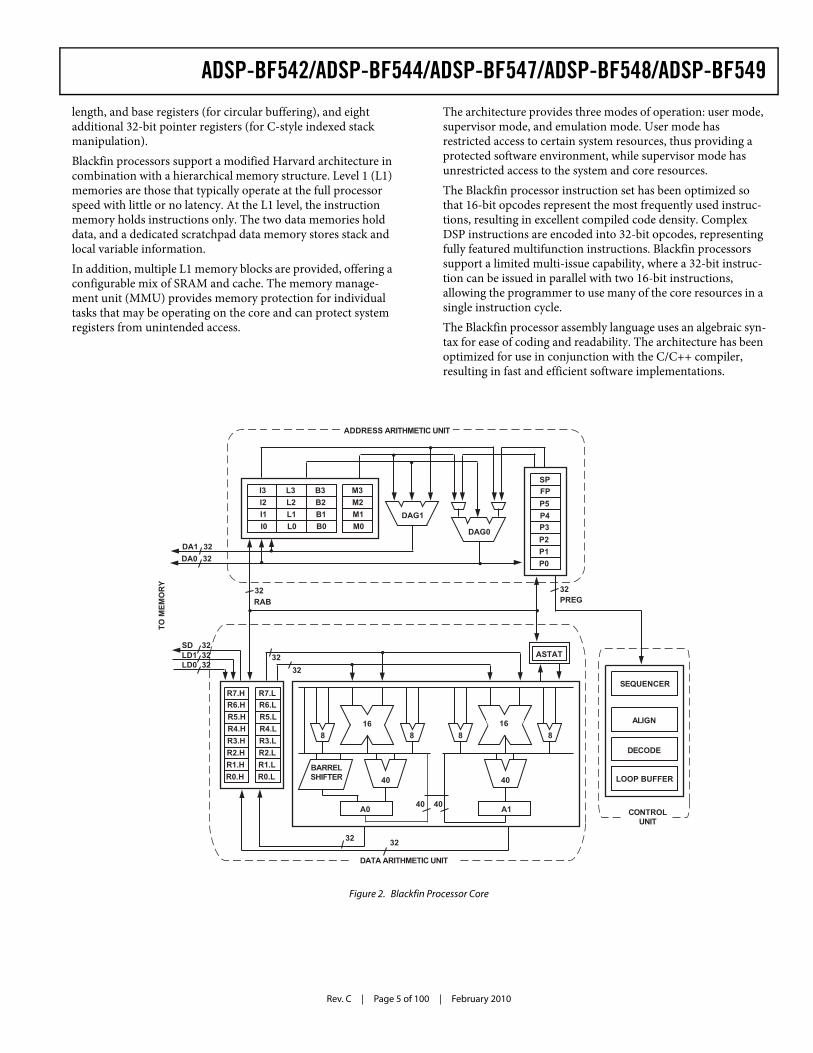
BLACKFIN PROCESSOR COREAs shown in Figure 2 on Page 5, the Blackfin processor core contains two 16-bit multipliers, two 40-bit accumulators, two 40-bit ALUs, four video ALUs, and a 40-bit shifter. The compu-tation units process 8-, 16-, or 32-bit data from the register file.The compute register file contains eight 32-bit registers. When performing compute operations on 16-bit operand data, the register file operates as 16 independent 16-bit registers. All operands for compute operations come from the multiported register file and instruction constant fields.Each MAC can perform a 16-bit by 16-bit multiply in each cycle, accumulating the results into the 40-bit accumulators. Signed and unsigned formats, rounding, and saturation are supported.The ALUs perform a traditional set of arithmetic and logical operations on 16- or 32-bit data. In addition, many special instructions are included to accelerate various signal processing tasks. These include bit operations such as field extract and pop-ulation count, modulo 232 multiply, divide primitives, saturation and rounding, and sign/exponent detection. The set of video instructions include byte alignment and packing operations, 16-bit and 8-bit adds with clipping, 8-bit average operations, and 8-bit subtract/absolute value/accumulate (SAA) operations. Also provided are the compare/select and vector search instructions.For certain instructions, two 16-bit ALU operations can be per-formed simultaneously on register pairs (a 16-bit high half and 16-bit low half of a compute register). By also using the second ALU, quad 16-bit operations are possible.The 40-bit shifter can perform shifts and rotates and is used to support normalization, field extract, and field deposit instructions.The program sequencer controls the flow of instruction execu-tion, including instruction alignment and decoding. For program flow control, the sequencer supports PC relative and indirect conditional jumps (with static branch prediction), and subroutine calls. Hardware is provided to support zero-over-head looping. The architecture is fully interlocked, meaning that the programmer need not manage the pipeline when executing instructions with data dependencies.The address arithmetic unit provides two addresses for simulta-neous dual fetches from memory. It contains a multiported register file consisting of four sets of 32-bit index, modify,
ADSP-BF542/ADSP-BF544/ADSP-BF547/ADSP-BF548/ADSP-BF549
Rev. C | Page 5 of 100 | February 2010
length, and base registers (for circular buffering), and eight additional 32-bit pointer registers (for C-style indexed stack manipulation).Blackfin processors support a modified Harvard architecture in combination with a hierarchical memory structure. Level 1 (L1) memories are those that typically operate at the full processor speed with little or no latency. At the L1 level, the instruction memory holds instructions only. The two data memories hold data, and a dedicated scratchpad data memory stores stack and local variable information.In addition, multiple L1 memory blocks are provided, offering a configurable mix of SRAM and cache. The memory manage-ment unit (MMU) provides memory protection for individual tasks that may be operating on the core and can protect system registers from unintended access.
The architecture provides three modes of operation: user mode, supervisor mode, and emulation mode. User mode has restricted access to certain system resources, thus providing a protected software environment, while supervisor mode has unrestricted access to the system and core resources.The Blackfin processor instruction set has been optimized so that 16-bit opcodes represent the most frequently used instruc-tions, resulting in excellent compiled code density. Complex DSP instructions are encoded into 32-bit opcodes, representing fully featured multifunction instructions. Blackfin processors support a limited multi-issue capability, where a 32-bit instruc-tion can be issued in parallel with two 16-bit instructions, allowing the programmer to use many of the core resources in a single instruction cycle.The Blackfin processor assembly language uses an algebraic syn-tax for ease of coding and readability. The architecture has been optimized for use in conjunction with the C/C++ compiler, resulting in fast and efficient software implementations.
Figure 2. Blackfin Processor Core
SEQUENCER
ALIGN
DECODE
LOOP BUFFER
16 16
88 8 8
40 40
A0 A1
BARRELSHIFTER
DATA ARITHMETIC UNIT
CONTROLUNIT
R7.HR6.H
R5.H
R4.H
R3.H
R2.H
R1.H
R0.H
R7.LR6.L
R5.L
R4.L
R3.L
R2.L
R1.L
R0.L
ASTAT
40 40
32 32
32
32
323232LD0
LD1SD
DAG0
DAG1
ADDRESS ARITHMETIC UNIT
I3
I2
I1
I0
L3
L2
L1
L0
B3
B2
B1
B0
M3
M2
M1
M0
SPFP
P5
P4P3
P2
P1
P0
DA1
DA0
32
32
32
PREGRAB32
TO
ME
MO
RY
Rev. C | Page 6 of 100 | February 2010
ADSP-BF542/ADSP-BF544/ADSP-BF547/ADSP-BF548/ADSP-BF549
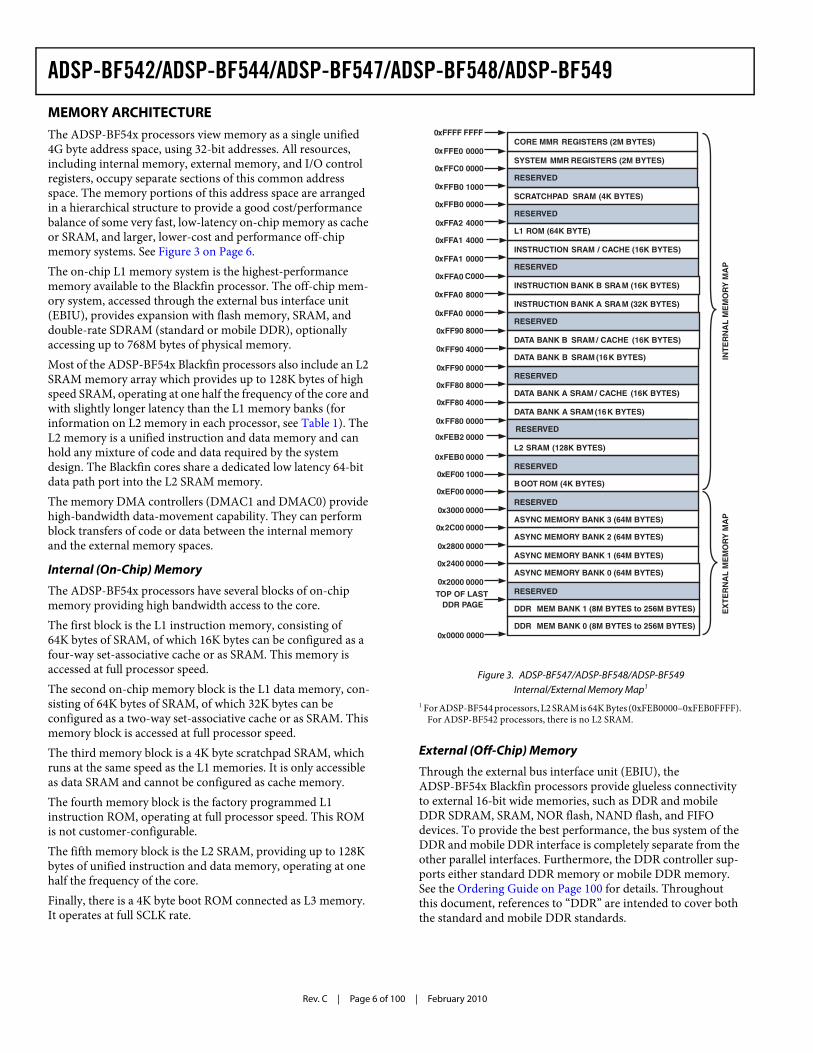
MEMORY ARCHITECTUREThe ADSP-BF54x processors view memory as a single unified 4G byte address space, using 32-bit addresses. All resources, including internal memory, external memory, and I/O control registers, occupy separate sections of this common address space. The memory portions of this address space are arranged in a hierarchical structure to provide a good cost/performance balance of some very fast, low-latency on-chip memory as cache or SRAM, and larger, lower-cost and performance off-chip memory systems. See Figure 3 on Page 6.The on-chip L1 memory system is the highest-performance memory available to the Blackfin processor. The off-chip mem-ory system, accessed through the external bus interface unit (EBIU), provides expansion with flash memory, SRAM, and double-rate SDRAM (standard or mobile DDR), optionally accessing up to 768M bytes of physical memory.Most of the ADSP-BF54x Blackfin processors also include an L2 SRAM memory array which provides up to 128K bytes of high speed SRAM, operating at one half the frequency of the core and with slightly longer latency than the L1 memory banks (for information on L2 memory in each processor, see Table 1). The L2 memory is a unified instruction and data memory and can hold any mixture of code and data required by the system design. The Blackfin cores share a dedicated low latency 64-bit data path port into the L2 SRAM memory.The memory DMA controllers (DMAC1 and DMAC0) provide high-bandwidth data-movement capability. They can perform block transfers of code or data between the internal memory and the external memory spaces.
Internal (On-Chip) Memory
The ADSP-BF54x processors have several blocks of on-chip memory providing high bandwidth access to the core. The first block is the L1 instruction memory, consisting of 64K bytes of SRAM, of which 16K bytes can be configured as a four-way set-associative cache or as SRAM. This memory is accessed at full processor speed.The second on-chip memory block is the L1 data memory, con-sisting of 64K bytes of SRAM, of which 32K bytes can be configured as a two-way set-associative cache or as SRAM. This memory block is accessed at full processor speed.The third memory block is a 4K byte scratchpad SRAM, which runs at the same speed as the L1 memories. It is only accessible as data SRAM and cannot be configured as cache memory. The fourth memory block is the factory programmed L1 instruction ROM, operating at full processor speed. This ROM is not customer-configurable. The fifth memory block is the L2 SRAM, providing up to 128K bytes of unified instruction and data memory, operating at one half the frequency of the core.Finally, there is a 4K byte boot ROM connected as L3 memory. It operates at full SCLK rate.
External (Off-Chip) Memory
Through the external bus interface unit (EBIU), the ADSP-BF54x Blackfin processors provide glueless connectivity to external 16-bit wide memories, such as DDR and mobile DDR SDRAM, SRAM, NOR flash, NAND flash, and FIFO devices. To provide the best performance, the bus system of the DDR and mobile DDR interface is completely separate from the other parallel interfaces. Furthermore, the DDR controller sup-ports either standard DDR memory or mobile DDR memory. See the Ordering Guide on Page 100 for details. Throughout this document, references to “DDR” are intended to cover both the standard and mobile DDR standards.
Figure 3. ADSP-BF547/ADSP-BF548/ADSP-BF549 Internal/External Memory Map1
1 For ADSP-BF544 processors, L2 SRAM is 64K Bytes (0xFEB0000–0xFEB0FFFF). For ADSP-BF542 processors, there is no L2 SRAM.
RESERVED
CORE MMR REGISTERS (2M BYTES)
RESERVED
SCRATCHPAD SRAM (4K BYTES)
INSTRUCTION BANK B SRAM (16K BYTES)
SYSTEM MMR REGISTERS (2M BYTES)
RESERVED
RESERVED
DATA BANK B SRAM / CACHE (16K BYTES)
DATA BANK B SRAM (16K BYTES)
DATA BANK A SRAM / CACHE (16K BYTES)
ASYNC MEMORY BANK 3 (64M BYTES)
ASYNC MEMORY BANK 2 (64M BYTES)
ASYNC MEMORY BANK 1 (64M BYTES)
ASYNC MEMORY BANK 0 (64M BYTES)
DDR MEM BANK 0 (8M BYTES to 256M BYTES)
INSTRUCTION SRAM / CACHE (16K BYTES)
INT
ER
NA
L M
EM
OR
Y M
AP
EX
TE
RN
AL
ME
MO
RY
MA
P
FFFF FFFF
FEB0 0000
FFB0 0000
FFA2 4000
FFA1 0000
FF90 8000
FF90 4000
FF80 8000
FF80 4000
3000 0000
2C00 0000
2800 0000
2400 0000
2000 0000
EF00 0000
0000 0000
FFC0 0000
FFB0 1000
FFA0 0000
DATA BANK A SRAM (16K BYTES)
FF90 0000
FF80 0000
RESERVED
RESERVEDC000
FFA0 8000INSTRUCTION BANK A SRAM (32K BYTES)
RESERVED
BOOT ROM (4K BYTES)EF00 1000
FFE0 0000
FEB2 0000
FFA1 4000L1 ROM (64K BYTE)
L2 SRAM (128K BYTES)
DDR MEM BANK 1 (8M BYTES to 256M BYTES)
RESERVEDTOP OF LASTDDR PAGE
RESERVED
FFA0
0x
0x
0x
0x
0x
0x
0x
0x
0x
0x
0x
0x
0x
0x
0x
0x
0x
0x
0x
0x
0x
0x
0x
0x
0x
0x
0x
ADSP-BF542/ADSP-BF544/ADSP-BF547/ADSP-BF548/ADSP-BF549
Rev. C | Page 7 of 100 | February 2010
The DDR memory controller can gluelessly manage up to two banks of double-rate synchronous dynamic memory (DDR and mobile DDR SDRAM). The 16-bit interface operates at the SCLK frequency, enabling a maximum throughput of 532M bytes/s. The DDR and mobile DDR controller is augmented with a queuing mechanism that performs efficient bursts into the DDR and mobile DDR. The controller is an industry stan-dard DDR and mobile DDR SDRAM controller with each bank supporting from 64M bit to 512M bit device sizes and 4-, 8-, or 16-bit widths. The controller supports up to 256M bytes per external bank. With 2 external banks, the controller supports up to 512M bytes total. Each bank is independently programmable and is contiguous with adjacent banks regardless of the sizes of the different banks or their placement. Traditional 16-bit asynchronous memories, such as SRAM, EPROM, and flash devices, can be connected to one of the four 64M byte asynchronous memory banks, represented by four memory select strobes. Alternatively, these strobes can function as bank-specific read or write strobes preventing further glue logic when connecting to asynchronous FIFO devices. See the Ordering Guide on Page 100 for a list of specific products that provide support for DDR memory.In addition, the external bus can connect to advanced flash device technologies, such as:
• Page-mode NOR flash devices• Synchronous burst-mode NOR flash devices• NAND flash devices
Customers should consult the Ordering Guide when selecting a specific ADSP-BF54x component for the intended application. Products that provide support for mobile DDR memory are noted in the ordering guide footnotes.
NAND Flash Controller (NFC)The ADSP-BF54x Blackfin processors provide a NAND Flash Controller (NFC) as part of the external bus interface. NAND flash devices provide high-density, low-cost memory. However, NAND flash devices also have long random access times, invalid blocks, and lower reliability over device lifetimes. Because of this, NAND flash is often used for read-only code storage. In this case, all DSP code can be stored in NAND flash and then transferred to a faster memory (such as DDR or SRAM) before execution. Another common use of NAND flash is for storage of multimedia files or other large data segments. In this case, a software file system may be used to manage reading and writing of the NAND flash device. The file system selects memory seg-ments for storage with the goal of avoiding bad blocks and equally distributing memory accesses across all address loca-tions. Hardware features of the NFC include:
• Support for page program, page read, and block erase of NAND flash devices, with accesses aligned to page boundaries.
• Error checking and correction (ECC) hardware that facili-tates error detection and correction.
• A single 8-bit or 16-bit external bus interface for com-mands, addresses, and data.
• Support for SLC (single level cell) NAND flash devices unlimited in size, with page sizes of 256 bytes and 512 bytes. Larger page sizes can be supported in software.
• The ability to release external bus interface pins during long accesses.
• Support for internal bus requests of 16 bits or 32 bits.• A DMA engine to transfer data between internal memory
and a NAND flash device.
One-Time-Programmable Memory
The ADSP-BF54x Blackfin processors have 64K bits of one-time-programmable (OTP) non-volatile memory that can be programmed by the developer only one time. It includes the array and logic to support read access and programming. Addi-tionally, its pages can be write protected. OTP enables developers to store both public and private data on-chip. In addition to storing public and private key data for applications requiring security, it also allows developers to store completely user-definable data such as a customer ID, product ID, or a MAC address. By using this feature, generic parts can be shipped, which are then programmed and protected by the developer within this non-volatile memory. The OTP memory can be accessed through an API provided by the on-chip ROM.
I/O Memory Space
The ADSP-BF54x Blackfin processors do not define a separate I/O space. All resources are mapped through the flat 32-bit address space. On-chip I/O devices have their control registers mapped into memory-mapped registers (MMRs) at addresses near the top of the 4G byte address space. These are separated into two smaller blocks, one containing the control MMRs for all core functions and the other containing the registers needed for setup and control of the on-chip peripherals outside of the core. The MMRs are accessible only in supervisor mode and appear as reserved space to on-chip peripherals.
Booting
The ADSP-BF54x Blackfin processors contain a small on-chip boot kernel, which configures the appropriate peripheral for booting. If the ADSP-BF54x Blackfin processors are configured to boot from boot ROM memory space, the processor starts exe-cuting from the on-chip boot ROM. For more information, see Booting Modes on Page 19.
Event Handling
The event controller on the ADSP-BF54x Blackfin processors handles all asynchronous and synchronous events to the proces-sors. The ADSP-BF54x Blackfin processors provide event handling that supports both nesting and prioritization. Nesting allows multiple event service routines to be active simulta-neously. Prioritization ensures that servicing of a
Rev. C | Page 8 of 100 | February 2010
ADSP-BF542/ADSP-BF544/ADSP-BF547/ADSP-BF548/ADSP-BF549
higher-priority event takes precedence over servicing of a lower-priority event. The controller provides support for five different types of events:
• Emulation. An emulation event causes the processor to enter emulation mode, allowing command and control of the processor via the JTAG interface.
• Reset. This event resets the processor.• Non-maskable interrupt (NMI). The NMI event can be
generated by the software watchdog timer or by the NMI input signal to the processor. The NMI event is frequently used as a power-down indicator to initiate an orderly shut-down of the system.
• Exceptions. Events that occur synchronously to program flow (that is, the exception is taken before the instruction is allowed to complete). Conditions such as data alignment violations and undefined instructions cause exceptions.
• Interrupts. Events that occur asynchronously to program flow. They are caused by input pins, timers, and other peripherals, as well as by an explicit software instruction.
Each event type has an associated register to hold the return address and an associated return-from-event instruction. When an event is triggered, the state of the processor is saved on the supervisor stack.The ADSP-BF54x Blackfin processor event controller consists of two stages, the core event controller (CEC) and the system interrupt controller (SIC). The core event controller works with the system interrupt controller to prioritize and control all sys-tem events. Conceptually, interrupts from the peripherals enter into the SIC and are then routed directly into the general-pur-pose interrupts of the CEC.
Core Event Controller (CEC)
The CEC supports nine general-purpose interrupts (IVG15–7), in addition to the dedicated interrupt and exception events. Of these general-purpose interrupts, the two lowest-priority inter-rupts (IVG15–14) are recommended to be reserved for software interrupt handlers, leaving seven prioritized interrupt inputs to support the peripherals of the ADSP-BF54x Blackfin processors. Table 3 describes the inputs to the CEC, identifies their names in the event vector table (EVT), and lists their priorities.
System Interrupt Controller (SIC)
The system interrupt controller provides the mapping and rout-ing of events from the many peripheral interrupt sources to the prioritized general-purpose interrupt inputs of the CEC. Although the ADSP-BF54x Blackfin processors provide a default mapping, the user can alter the mappings and priorities of interrupt events by writing the appropriate values into the interrupt assignment registers (SIC_IARx). Table 4 describes the inputs into the SIC and the default mappings into the CEC.
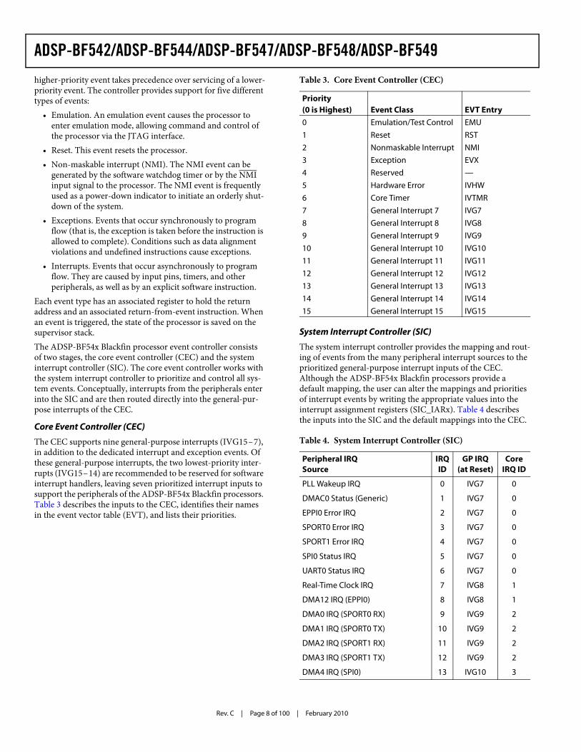
Table 3. Core Event Controller (CEC)
Priority(0 is Highest) Event Class EVT Entry0 Emulation/Test Control EMU1 Reset RST2 Nonmaskable Interrupt NMI3 Exception EVX4 Reserved —5 Hardware Error IVHW6 Core Timer IVTMR7 General Interrupt 7 IVG78 General Interrupt 8 IVG89 General Interrupt 9 IVG910 General Interrupt 10 IVG1011 General Interrupt 11 IVG1112 General Interrupt 12 IVG1213 General Interrupt 13 IVG1314 General Interrupt 14 IVG1415 General Interrupt 15 IVG15
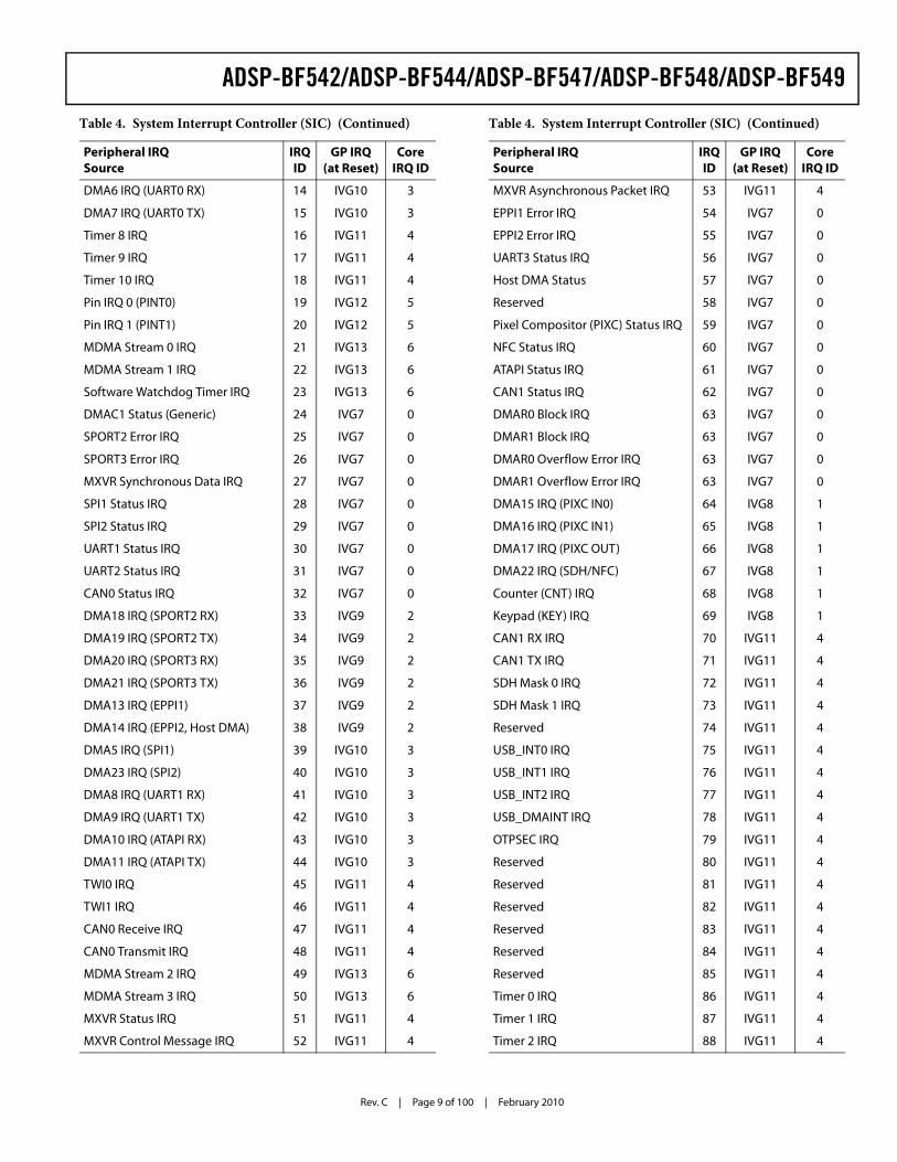
Table 4. System Interrupt Controller (SIC)
Peripheral IRQSource
IRQID
GP IRQ(at Reset)
CoreIRQ ID
PLL Wakeup IRQ 0 IVG7 0
DMAC0 Status (Generic) 1 IVG7 0
EPPI0 Error IRQ 2 IVG7 0
SPORT0 Error IRQ 3 IVG7 0
SPORT1 Error IRQ 4 IVG7 0
SPI0 Status IRQ 5 IVG7 0
UART0 Status IRQ 6 IVG7 0
Real-Time Clock IRQ 7 IVG8 1
DMA12 IRQ (EPPI0) 8 IVG8 1
DMA0 IRQ (SPORT0 RX) 9 IVG9 2
DMA1 IRQ (SPORT0 TX) 10 IVG9 2
DMA2 IRQ (SPORT1 RX) 11 IVG9 2
DMA3 IRQ (SPORT1 TX) 12 IVG9 2
DMA4 IRQ (SPI0) 13 IVG10 3
ADSP-BF542/ADSP-BF544/ADSP-BF547/ADSP-BF548/ADSP-BF549
Rev. C | Page 9 of 100 | February 2010
DMA6 IRQ (UART0 RX) 14 IVG10 3
DMA7 IRQ (UART0 TX) 15 IVG10 3
Timer 8 IRQ 16 IVG11 4
Timer 9 IRQ 17 IVG11 4
Timer 10 IRQ 18 IVG11 4
Pin IRQ 0 (PINT0) 19 IVG12 5
Pin IRQ 1 (PINT1) 20 IVG12 5
MDMA Stream 0 IRQ 21 IVG13 6
MDMA Stream 1 IRQ 22 IVG13 6
Software Watchdog Timer IRQ 23 IVG13 6
DMAC1 Status (Generic) 24 IVG7 0
SPORT2 Error IRQ 25 IVG7 0
SPORT3 Error IRQ 26 IVG7 0
MXVR Synchronous Data IRQ 27 IVG7 0
SPI1 Status IRQ 28 IVG7 0
SPI2 Status IRQ 29 IVG7 0
UART1 Status IRQ 30 IVG7 0
UART2 Status IRQ 31 IVG7 0
CAN0 Status IRQ 32 IVG7 0
DMA18 IRQ (SPORT2 RX) 33 IVG9 2
DMA19 IRQ (SPORT2 TX) 34 IVG9 2
DMA20 IRQ (SPORT3 RX) 35 IVG9 2
DMA21 IRQ (SPORT3 TX) 36 IVG9 2
DMA13 IRQ (EPPI1) 37 IVG9 2
DMA14 IRQ (EPPI2, Host DMA) 38 IVG9 2
DMA5 IRQ (SPI1) 39 IVG10 3
DMA23 IRQ (SPI2) 40 IVG10 3
DMA8 IRQ (UART1 RX) 41 IVG10 3
DMA9 IRQ (UART1 TX) 42 IVG10 3
DMA10 IRQ (ATAPI RX) 43 IVG10 3
DMA11 IRQ (ATAPI TX) 44 IVG10 3
TWI0 IRQ 45 IVG11 4
TWI1 IRQ 46 IVG11 4
CAN0 Receive IRQ 47 IVG11 4
CAN0 Transmit IRQ 48 IVG11 4
MDMA Stream 2 IRQ 49 IVG13 6
MDMA Stream 3 IRQ 50 IVG13 6
MXVR Status IRQ 51 IVG11 4
MXVR Control Message IRQ 52 IVG11 4
Table 4. System Interrupt Controller (SIC) (Continued)
Peripheral IRQSource
IRQID
GP IRQ(at Reset)
CoreIRQ ID
MXVR Asynchronous Packet IRQ 53 IVG11 4
EPPI1 Error IRQ 54 IVG7 0
EPPI2 Error IRQ 55 IVG7 0
UART3 Status IRQ 56 IVG7 0
Host DMA Status 57 IVG7 0
Reserved 58 IVG7 0
Pixel Compositor (PIXC) Status IRQ 59 IVG7 0
NFC Status IRQ 60 IVG7 0
ATAPI Status IRQ 61 IVG7 0
CAN1 Status IRQ 62 IVG7 0
DMAR0 Block IRQ 63 IVG7 0
DMAR1 Block IRQ 63 IVG7 0
DMAR0 Overflow Error IRQ 63 IVG7 0
DMAR1 Overflow Error IRQ 63 IVG7 0
DMA15 IRQ (PIXC IN0) 64 IVG8 1
DMA16 IRQ (PIXC IN1) 65 IVG8 1
DMA17 IRQ (PIXC OUT) 66 IVG8 1
DMA22 IRQ (SDH/NFC) 67 IVG8 1
Counter (CNT) IRQ 68 IVG8 1
Keypad (KEY) IRQ 69 IVG8 1
CAN1 RX IRQ 70 IVG11 4
CAN1 TX IRQ 71 IVG11 4
SDH Mask 0 IRQ 72 IVG11 4
SDH Mask 1 IRQ 73 IVG11 4
Reserved 74 IVG11 4
USB_INT0 IRQ 75 IVG11 4
USB_INT1 IRQ 76 IVG11 4
USB_INT2 IRQ 77 IVG11 4
USB_DMAINT IRQ 78 IVG11 4
OTPSEC IRQ 79 IVG11 4
Reserved 80 IVG11 4
Reserved 81 IVG11 4
Reserved 82 IVG11 4
Reserved 83 IVG11 4
Reserved 84 IVG11 4
Reserved 85 IVG11 4
Timer 0 IRQ 86 IVG11 4
Timer 1 IRQ 87 IVG11 4
Timer 2 IRQ 88 IVG11 4
Table 4. System Interrupt Controller (SIC) (Continued)
Peripheral IRQSource
IRQID
GP IRQ(at Reset)
CoreIRQ ID
Rev. C | Page 10 of 100 | February 2010
ADSP-BF542/ADSP-BF544/ADSP-BF547/ADSP-BF548/ADSP-BF549
Event Control
The ADSP-BF54x Blackfin processors provide the user with a very flexible mechanism to control the processing of events. In the CEC, three registers are used to coordinate and control events. Each register is 16 bits wide:
• CEC interrupt latch register (ILAT). The ILAT register indicates when events have been latched. The appropriate bit is set when the processor has latched the event and cleared when the event has been accepted into the system. This register is updated automatically by the controller, but it may be written only when its corresponding IMASK bit is cleared.
• CEC interrupt mask register (IMASK). The IMASK regis-ter controls the masking and unmasking of individual events. When a bit is set in the IMASK register, that event is unmasked and is processed by the CEC when asserted. A cleared bit in the IMASK register masks the event, prevent-ing the processor from servicing the event even though the event may be latched in the ILAT register. This register may be read or written while in supervisor mode. Note that general-purpose interrupts can be globally enabled and dis-abled with the STI and CLI instructions, respectively.
• CEC interrupt pending register (IPEND). The IPEND reg-ister keeps track of all nested events. A set bit in the IPEND register indicates that the event is currently active or nested at some level. This register is updated automatically by the controller but may be read while in supervisor mode.
The SIC allows further control of event processing by providing three 32-bit interrupt control and status registers. Each register contains a bit corresponding to each of the peripheral interrupt events shown in Table 4 on Page 8.
• SIC interrupt mask registers (SIC_IMASKx). These regis-ters control the masking and unmasking of each peripheral interrupt event. When a bit is set in a register, that periph-eral event is unmasked and is processed by the system when asserted. A cleared bit in the register masks the peripheral event, preventing the processor from servicing the event.
• SIC interrupt status registers (SIC_ISRx). As multiple peripherals can be mapped to a single event, these registers allow the software to determine which peripheral event
source triggered the interrupt. A set bit indicates the peripheral is asserting the interrupt, and a cleared bit indi-cates the peripheral is not asserting the event.
• SIC interrupt wakeup enable registers (SIC_IWRx). By enabling the corresponding bit in this register, a peripheral can be configured to wake up the processor, should the core be idled or in Sleep mode when the event is generated. (For more information, see Dynamic Power Management on Page 16.)
Because multiple interrupt sources can map to a single general-purpose interrupt, multiple pulse assertions can occur simulta-neously, before or during interrupt processing for an interrupt event already detected on this interrupt input. The IPEND reg-ister contents are monitored by the SIC as the interrupt acknowledgement.The appropriate ILAT register bit is set when an interrupt rising edge is detected. (Detection requires two core clock cycles.) The bit is cleared when the respective IPEND register bit is set. The IPEND bit indicates that the event has entered into the proces-sor pipeline. At this point the CEC recognizes and queues the next rising edge event on the corresponding event input. The minimum latency from the rising edge transition of the general-purpose interrupt to the IPEND output asserted is three core clock cycles; however, the latency can be much higher, depend-ing on the activity within and the state of the processor.
DMA CONTROLLERSADSP-BF54x Blackfin processors have multiple, independent DMA channels that support automated data transfers with min-imal overhead for the processor core. DMA transfers can occur between the ADSP-BF54x processors’ internal memories and any of the DMA-capable peripherals. Additionally, DMA trans-fers can be accomplished between any of the DMA-capable peripherals and external devices connected to the external memory interfaces, including DDR and asynchronous memory controllers.While the USB controller and MXVR have their own dedicated DMA controllers, the other on-chip peripherals are managed by two centralized DMA controllers, called DMAC1 (32-bit) and DMAC0 (16-bit). Both operate in the SCLK domain. Each DMA controller manages 12 independent peripheral DMA channels, as well as two independent memory DMA streams. The DMAC1 controller masters high-bandwidth peripherals over a dedicated 32-bit DMA access bus (DAB32). Similarly, the DMAC0 controller masters most serial interfaces over the 16-bit DAB16 bus. Individual DMA channels have fixed access prior-ity on the DAB buses. DMA priority of peripherals is managed by a flexible peripheral-to-DMA channel assignment scheme. All four DMA controllers use the same 32-bit DCB bus to exchange data with L1 memory. This includes L1 ROM, but excludes scratchpad memory. Fine granulation of L1 memory and special DMA buffers minimize potential memory conflicts when the L1 memory is accessed simultaneously by the core. Similarly, there are dedicated DMA buses between the external bus interface unit (EBIU) and the three DMA controllers (DMAC1, DMAC0, and USB) that arbitrate DMA accesses to external memories and the boot ROM.
Timer 3 IRQ 89 IVG11 4
Timer 4 IRQ 90 IVG11 4
Timer 5 IRQ 91 IVG11 4
Timer 6 IRQ 92 IVG11 4
Timer 7 IRQ 93 IVG11 4
Pin IRQ 2 (PINT2) 94 IVG12 5
Pin IRQ 3 (PINT3) 95 IVG12 5
Table 4. System Interrupt Controller (SIC) (Continued)
Peripheral IRQSource
IRQID
GP IRQ(at Reset)
CoreIRQ ID
ADSP-BF542/ADSP-BF544/ADSP-BF547/ADSP-BF548/ADSP-BF549
Rev. C | Page 11 of 100 | February 2010
The ADSP-BF54x Blackfin processors’ DMA controllers sup-port both 1-dimensional (1D) and 2-dimensional (2D) DMA transfers. DMA transfer initialization can be implemented from registers or from sets of parameters called descriptor blocks.The 2D DMA capability supports arbitrary row and column sizes up to 64K elements by 64K elements, and arbitrary row and column step sizes up to ±32K elements. Furthermore, the column step size can be less than the row step size, allowing implementation of interleaved data streams. This feature is especially useful in video applications where data can be de-interleaved on the fly.Examples of DMA types supported by the ADSP-BF54x Blackfin processors’ DMA controllers include:
• A single, linear buffer that stops upon completion• A circular, auto-refreshing buffer that interrupts on each
full or fractionally full buffer• 1D or 2D DMA using a linked list of descriptors• 2D DMA using an array of descriptors, specifying only the
base DMA address within a common pageIn addition to the dedicated peripheral DMA channels, the DMAC1 and DMAC0 controllers each feature two memory DMA channel pairs for transfers between the various memories of the ADSP-BF54x Blackfin processors. This enables transfers of blocks of data between any of the memories—including external DDR, ROM, SRAM, and flash memory—with minimal processor intervention. Like peripheral DMAs, memory DMA transfers can be controlled by a very flexible descriptor-based methodology or by a standard register-based autobuffer mechanism.The memory DMA channels of the DMAC1 controller (MDMA2 and MDMA3) can be controlled optionally by the external DMA request input pins. When used in conjunction with the External Bus Interface Unit (EBIU), this handshaked memory DMA (HMDMA) scheme can be used to efficiently exchange data with block-buffered or FIFO-style devices con-nected externally. Users can select whether the DMA request pins control the source or the destination side of the memory DMA. It allows control of the number of data transfers for memory DMA. The number of transfers per edge is program-mable. This feature can be programmed to allow memory DMA to have an increased priority on the external bus relative to the core.
Host DMA Port Interface
The host DMA port (HOSTDP) facilitates a host device external to the ADSP-BF54x Blackfin processors to be a DMA master and transfer data back and forth. The host device always masters the transactions, and the processor is always a DMA slave device.The HOSTDP is enabled through the peripheral access bus. Once the port has been enabled, the transactions are controlled by the external host. The external host programs standard DMA
configuration words in order to send/receive data to any valid internal or external memory location. The host DMA port con-troller includes the following features:
• Allows an external master to configure DMA read/write data transfers and read port status
• Uses a flexible asynchronous memory protocol for its external interface
• Allows an 8- or 16-bit external data interface to the host device
• Supports half-duplex operation• Supports little/big endian data transfers• Acknowledge mode allows flow control on host
transactions• Interrupt mode guarantees a burst of FIFO depth host
transactions
REAL-TIME CLOCKThe ADSP-BF54x Blackfin processors’ real-time clock (RTC) provides a robust set of digital watch features, including current time, stopwatch, and alarm. The RTC is clocked by a 32.768 kHz crystal external to the ADSP-BF54x Blackfin processors. The RTC peripheral has dedicated power supply pins so that it can remain powered up and clocked even when the rest of the pro-cessor is in a low-power state. The RTC provides several programmable interrupt options, including interrupt per sec-ond, minute, hour, or day clock ticks, interrupt on programmable stopwatch countdown, or interrupt at a pro-grammed alarm time.The 32.768 kHz input clock frequency is divided down to a 1 Hz signal by a prescaler. The counter function of the timer consists of four counters: a 60-second counter, a 60-minute counter, a 24-hour counter, and a 32,768-day counter.When enabled, the alarm function generates an interrupt when the output of the timer matches the programmed value in the alarm control register. There are two alarms. The first alarm is for a time of day. The second alarm is for a day and time of that day.The stopwatch function counts down from a programmed value with one-second resolution. When the stopwatch is enabled and the counter underflows, an interrupt is generated.Like the other peripherals, the RTC can wake up the ADSP-BF54x processor from sleep mode upon generation of any RTC wakeup event. Additionally, an RTC wakeup event can wake up the ADSP-BF54x processors from deep sleep mode, and it can wake up the on-chip internal voltage regulator from the hibernate state.
Rev. C | Page 12 of 100 | February 2010
ADSP-BF542/ADSP-BF544/ADSP-BF547/ADSP-BF548/ADSP-BF549
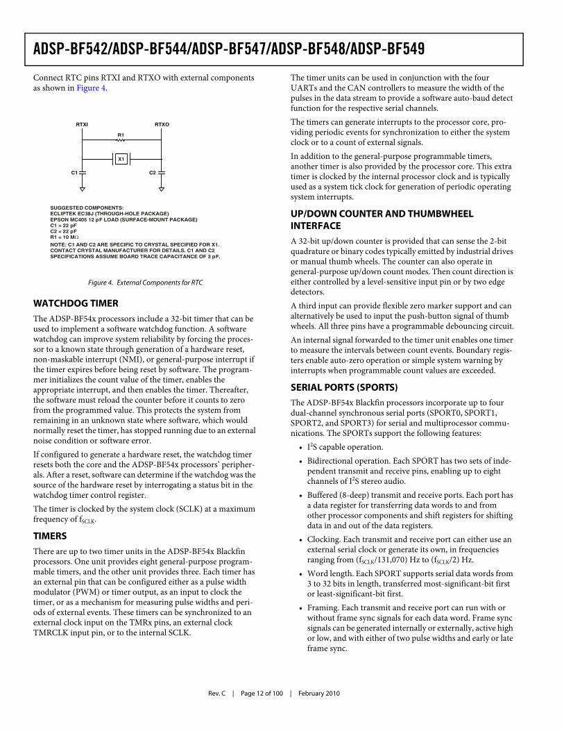
Connect RTC pins RTXI and RTXO with external components as shown in Figure 4.
WATCHDOG TIMERThe ADSP-BF54x processors include a 32-bit timer that can be used to implement a software watchdog function. A software watchdog can improve system reliability by forcing the proces-sor to a known state through generation of a hardware reset, non-maskable interrupt (NMI), or general-purpose interrupt if the timer expires before being reset by software. The program-mer initializes the count value of the timer, enables the appropriate interrupt, and then enables the timer. Thereafter, the software must reload the counter before it counts to zero from the programmed value. This protects the system from remaining in an unknown state where software, which would normally reset the timer, has stopped running due to an external noise condition or software error.If configured to generate a hardware reset, the watchdog timer resets both the core and the ADSP-BF54x processors’ peripher-als. After a reset, software can determine if the watchdog was the source of the hardware reset by interrogating a status bit in the watchdog timer control register.The timer is clocked by the system clock (SCLK) at a maximum frequency of fSCLK.
TIMERSThere are up to two timer units in the ADSP-BF54x Blackfin processors. One unit provides eight general-purpose program-mable timers, and the other unit provides three. Each timer has an external pin that can be configured either as a pulse width modulator (PWM) or timer output, as an input to clock the timer, or as a mechanism for measuring pulse widths and peri-ods of external events. These timers can be synchronized to an external clock input on the TMRx pins, an external clock TMRCLK input pin, or to the internal SCLK.
The timer units can be used in conjunction with the four UARTs and the CAN controllers to measure the width of the pulses in the data stream to provide a software auto-baud detect function for the respective serial channels. The timers can generate interrupts to the processor core, pro-viding periodic events for synchronization to either the system clock or to a count of external signals.In addition to the general-purpose programmable timers, another timer is also provided by the processor core. This extra timer is clocked by the internal processor clock and is typically used as a system tick clock for generation of periodic operating system interrupts.
UP/DOWN COUNTER AND THUMBWHEEL INTERFACEA 32-bit up/down counter is provided that can sense the 2-bit quadrature or binary codes typically emitted by industrial drives or manual thumb wheels. The counter can also operate in general-purpose up/down count modes. Then count direction is either controlled by a level-sensitive input pin or by two edge detectors.A third input can provide flexible zero marker support and can alternatively be used to input the push-button signal of thumb wheels. All three pins have a programmable debouncing circuit.An internal signal forwarded to the timer unit enables one timer to measure the intervals between count events. Boundary regis-ters enable auto-zero operation or simple system warning by interrupts when programmable count values are exceeded.
SERIAL PORTS (SPORTS)The ADSP-BF54x Blackfin processors incorporate up to four dual-channel synchronous serial ports (SPORT0, SPORT1, SPORT2, and SPORT3) for serial and multiprocessor commu-nications. The SPORTs support the following features:
• I2S capable operation.• Bidirectional operation. Each SPORT has two sets of inde-
pendent transmit and receive pins, enabling up to eight channels of I2S stereo audio.
• Buffered (8-deep) transmit and receive ports. Each port has a data register for transferring data words to and from other processor components and shift registers for shifting data in and out of the data registers.
• Clocking. Each transmit and receive port can either use an external serial clock or generate its own, in frequencies ranging from (fSCLK/131,070) Hz to (fSCLK/2) Hz.
• Word length. Each SPORT supports serial data words from 3 to 32 bits in length, transferred most-significant-bit first or least-significant-bit first.
• Framing. Each transmit and receive port can run with or without frame sync signals for each data word. Frame sync signals can be generated internally or externally, active high or low, and with either of two pulse widths and early or late frame sync.
Figure 4. External Components for RTC
RTXO
C1 C2
X1
SUGGESTED COMPONENTS:ECLIPTEK EC38J (THROUGH-HOLE PACKAGE)EPSON MC405 12 pF LOAD (SURFACE-MOUNT PACKAGE)C1 = 22 pFC2 = 22 pFR1 = 10 M
NOTE: C1 AND C2 ARE SPECIFIC TO CRYSTAL SPECIFIED FOR X1.CONTACT CRYSTAL MANUFACTURER FOR DETAILS. C1 AND C2SPECIFICATIONS ASSUME BOARD TRACE CAPACITANCE OF 3 pF.
RTXI
R1
ADSP-BF542/ADSP-BF544/ADSP-BF547/ADSP-BF548/ADSP-BF549
Rev. C | Page 13 of 100 | February 2010
• Companding in hardware. Each SPORT can perform A-law or μ-law companding according to ITU recommen-dation G.711. Companding can be selected on the transmit and/or receive channel of the SPORT without additional latencies.
• DMA operations with single-cycle overhead. Each SPORT can receive and transmit multiple buffers of memory data automatically. The processor can link or chain sequences of DMA transfers between a SPORT and memory.
• Interrupts. Each transmit and receive port generates an interrupt upon completing the transfer of a data word or after transferring an entire data buffer or buffers through DMA.
• Multichannel capability. Each SPORT supports 128 chan-nels out of a 1024-channel window and is compatible with the H.100, H.110, MVIP-90, and HMVIP standards.
SERIAL PERIPHERAL INTERFACE (SPI) PORTSThe ADSP-BF54x Blackfin processors have up to three SPI-compatible ports that allow the processor to communicate with multiple SPI-compatible devices. Each SPI port uses three pins for transferring data: two data pins (master output slave input, SPIxMOSI, and master input-slave output, SPIxMISO) and a clock pin (serial clock, SPIxSCK). An SPI chip select input pin (SPIxSS) lets other SPI devices select the processor, and three SPI chip select output pins per SPI port SPIxSELy let the processor select other SPI devices. The SPI select pins are reconfigured general-purpose I/O pins. Using these pins, the SPI ports provide a full-duplex, synchronous serial interface, which supports both master/slave modes and multimaster environments. The SPI port’s baud rate and clock phase/polarities are pro-grammable, and it has an integrated DMA controller, configurable to support transmit or receive data streams. The SPI’s DMA controller can only service unidirectional accesses at any given time.The SPI port’s clock rate is calculated as
Where the 16-bit SPI_BAUD register contains a value of 2 to 65,535.During transfers, the SPI port transmits and receives simulta-neously by serially shifting data in and out on its two serial data lines. The serial clock line synchronizes the shifting and sam-pling of data on the two serial data lines.
UART PORTS (UARTS)The ADSP-BF54x Blackfin processors provide up to four full-duplex universal asynchronous receiver/transmitter (UART) ports. Each UART port provides a simplified UART interface to other peripherals or hosts, supporting full-duplex, DMA-sup-ported, asynchronous transfers of serial data. A UART port
includes support for five to eight data bits, one or two stop bits, and none, even, or odd parity. Each UART port supports two modes of operation:
• PIO (programmed I/O). The processor sends or receives data by writing or reading I/O-mapped UART registers. The data is double-buffered on both transmit and receive.
• DMA (direct memory access). The DMA controller trans-fers both transmit and receive data. This reduces the number and frequency of interrupts required to transfer data to and from memory. Each UART has two dedicated DMA channels, one for transmit and one for receive. These DMA channels have lower default priority than most DMA channels because of their relatively low service rates. Flexi-ble interrupt timing options are available on the transmit side.
Each UART port’s baud rate, serial data format, error code gen-eration and status, and interrupts are programmable:
• Supporting bit rates ranging from (fSCLK/1,048,576) to (fSCLK) bits per second.
• Supporting data formats from seven to 12 bits per frame.• Both transmit and receive operations can be configured to
generate maskable interrupts to the processor.The UART port’s clock rate is calculated as
Where the 16-bit UART divisor comes from the UARTx_DLH register (most significant 8 bits) and UARTx_DLL register (least significant eight bits), and the EDBO is a bit in the UARTx_GCTL register.In conjunction with the general-purpose timer functions, auto-baud detection is supported. UART1 and UART3 feature a pair of UARTxRTS (request to send) and UARTxCTS (clear to send) signals for hardware flow purposes. The transmitter hardware is automatically prevented from sending further data when the UARTxCTS input is de-asserted. The receiver can automatically de-assert its UARTxRTS output when the enhanced receive FIFO exceeds a certain high-water level. The capabilities of the UARTs are fur-ther extended with support for the Infrared Data Association (IrDA®) Serial Infrared Physical Layer Link Specification (SIR) protocol.
CONTROLLER AREA NETWORK (CAN) The ADSP-BF54x Blackfin processors offer up to two CAN con-trollers that are communication controllers that implement the controller area network (CAN) 2.0B (active) protocol. This pro-tocol is an asynchronous communications protocol used in both industrial and automotive control systems. The CAN protocol is well suited for control applications due to its capability to com-municate reliably over a network since the protocol incorporates CRC checking, message error tracking, and fault node confinement.
SPI Clock RatefSCLK
2 SPI_BAUD×------------------------------------=
UART Clock RatefSCLK
16 1 EDBO–( ) UART_Divisor×------------------------------------------------------------------------------=
Rev. C | Page 14 of 100 | February 2010
ADSP-BF542/ADSP-BF544/ADSP-BF547/ADSP-BF548/ADSP-BF549
The ADSP-BF54x Blackfin processors’ CAN controllers offer the following features:
• 32 mailboxes (8 receive only, 8 transmit only, 16 config-urable for receive or transmit).
• Dedicated acceptance masks for each mailbox.• Additional data filtering on first two bytes.• Support for both the standard (11-bit) and extended (29-
bit) identifier (ID) message formats.• Support for remote frames.• Active or passive network support.• CAN wakeup from hibernation mode (lowest static power
consumption mode).• Interrupts, including: TX complete, RX complete, error
and global.The electrical characteristics of each network connection are very demanding, so the CAN interface is typically divided into two parts: a controller and a transceiver. This allows a single controller to support different drivers and CAN networks. The ADSP-BF54x Blackfin processors’ CAN module represents only the controller part of the interface. The controller interface sup-ports connection to 3.3 V high speed, fault-tolerant, single-wire transceivers.An additional crystal is not required to supply the CAN clock, as the CAN clock is derived from the processor system clock (SCLK) through a programmable divider.
TWI CONTROLLER INTERFACE The ADSP-BF54x Blackfin processors include up to two 2-wire interface (TWI) modules for providing a simple exchange method of control data between multiple devices. The modules are compatible with the widely used I2C bus standard. The TWI modules offer the capabilities of simultaneous master and slave operation and support for both 7-bit addressing and multime-dia data arbitration. Each TWI interface uses two pins for transferring clock (SCLx) and data (SDAx), and supports the protocol at speeds up to 400K bits/sec. The TWI interface pins are compatible with 5 V logic levels.Additionally, the ADSP-BF54x Blackfin processors’ TWI mod-ules are fully compatible with serial camera control bus (SCCB) functionality for easier control of various CMOS camera sensor devices.
PORTS Because of their rich set of peripherals, the ADSP-BF54x Blackfin processors group the many peripheral signals to ten ports—referred to as Port A to Port J. Most ports contain 16 pins, though some have fewer. Many of the associated pins are shared by multiple signals. The ports function as multiplexer controls. Every port has its own set of memory-mapped regis-ters to control port muxing and GPIO functionality.
General-Purpose I/O (GPIO)
Every pin in Port A to Port J can function as a GPIO pin, result-ing in a GPIO pin count up to 154. While it is unlikely that all GPIO pins will be used in an application, as all pins have multi-ple functions, the richness of GPIO functionality guarantees unrestrictive pin usage. Every pin that is not used by any func-tion can be configured in GPIO mode on an individual basis.After reset, all pins are in GPIO mode by default. Since neither GPIO output nor input drivers are active by default, unused pins can be left unconnected. GPIO data and direction control registers provide flexible write-one-to-set and write-one-to-clear mechanisms so that independent software threads do not need to protect against each other because of expensive read-modify-write operations when accessing the same port.
Pin Interrupts
Every port pin on ADSP-BF54x Blackfin processors can request interrupts in either an edge-sensitive or a level-sensitive manner with programmable polarity. Interrupt functionality is decou-pled from GPIO operation. Four system-level interrupt channels (PINT0, PINT1, PINT2 and PINT3) are reserved for this purpose. Each of these interrupt channels can manage up to 32 interrupt pins. The assignment from pin to interrupt is not performed on a pin-by-pin basis. Rather, groups of eight pins (half ports) can be flexibly assigned to interrupt channels. Every pin interrupt channel features a special set of 32-bit mem-ory-mapped registers that enables half-port assignment and interrupt management. This not only includes masking, identi-fication, and clearing of requests, it also enables access to the respective pin states and use of the interrupt latches regardless of whether the interrupt is masked or not. Most control registers feature multiple MMR address entries to write-one-to-set or write-one-to-clear them individually.
PIXEL COMPOSITOR (PIXC)The pixel compositor (PIXC) provides image overlays with transparent-color support, alpha blending, and color space con-version capabilities for output to TFT LCDs and NTSC/PAL video encoders. It provides all of the control to allow two data streams from two separate data buffers to be combined, blended, and converted into appropriate forms for both LCD panels and digital video outputs. The main image buffer pro-vides the basic background image, which is presented in the data stream. The overlay image buffer allows the user to add multiple foreground text, graphics, or video objects on top of the main image or video data stream.
ENHANCED PARALLEL PERIPHERAL INTERFACE (EPPI)The ADSP-BF54x Blackfin processors provide up to three enhanced parallel peripheral interfaces (EPPIs), supporting data widths up to 24 bits. The EPPI supports direct connection to TFT LCD panels, parallel analog-to-digital and digital-to-ana-log converters, video encoders and decoders, image sensor modules and other general-purpose peripherals.
ADSP-BF542/ADSP-BF544/ADSP-BF547/ADSP-BF548/ADSP-BF549
Rev. C | Page 15 of 100 | February 2010
The following features are supported in the EPPI module:• Programmable data length: 8 bits, 10 bits, 12 bits, 14 bits,
16 bits, 18 bits, and 24 bits per clock.• Bidirectional and half-duplex port.• Clock can be provided externally or can be generated
internally.• Various framed and non-framed operating modes. Frame
syncs can be generated internally or can be supplied by an external device.
• Various general-purpose modes with zero to three frame syncs for both receive and transmit directions.
• ITU-656 status word error detection and correction for ITU-656 receive modes.
• ITU-656 preamble and status word decode. • Three different modes for ITU-656 receive modes: active
video only, vertical blanking only, and entire field mode.• Horizontal and vertical windowing for GP 2 and 3 frame
sync modes.• Optional packing and unpacking of data to/from 32 bits
from/to 8, 16 and 24 bits. If packing/unpacking is enabled, endianness can be changed to change the order of pack-ing/unpacking of bytes/words.
• Optional sign extension or zero fill for receive modes. • During receive modes, alternate even or odd data samples
can be filtered out.• Programmable clipping of data values for 8-bit transmit
modes.• RGB888 can be converted to RGB666 or RGB565 for trans-
mit modes.• Various de-interleaving/interleaving modes for receiv-
ing/transmitting 4:2:2 YCrCb data.• FIFO watermarks and urgent DMA features.• Clock gating by an external device asserting the clock gat-
ing control signal.• Configurable LCD data enable (DEN) output available on
Frame Sync 3.
USB ON-THE-GO DUAL-ROLE DEVICE CONTROLLERThe USB OTG dual-role device controller (USBDRC) provides a low-cost connectivity solution for consumer mobile devices such as cell phones, digital still cameras, and MP3 players, allowing these devices to transfer data using a point-to-point USB connection without the need for a PC host. The USBDRC module can operate in a traditional USB peripheral-only mode as well as the host mode presented in the On-the-Go (OTG) supplement to the USB 2.0 specification. In host mode, the USB module supports transfers at high speed (480 Mbps), full speed (12 Mbps), and low speed (1.5 Mbps) rates. Peripheral-only mode supports the high and full speed transfer rates.
The USB clock (USB_XI) is provided through a dedicated exter-nal crystal or crystal oscillator. See Table 62 for related timing requirements. If using a fundamental mode crystal to provide the USB clock, connect the crystal between USB_XI and USB_XO with a circuit similar to that shown in Figure 7. Use a parallel-resonant, fundamental mode, microprocessor-grade crystal. If a third-overtone crystal is used, follow the circuit guidelines outlined in Clock Signals on Page 18 for third-over-tone crystals.The USB On-the-Go dual-role device controller includes a Phase Locked Loop with programmable multipliers to generate the necessary internal clocking frequency for USB. The multi-plier value should be programmed based on the USB_XI clock frequency to achieve the necessary 480 MHz internal clock for USB high speed operation. For example, for a USB_XI crystal frequency of 24 MHz, the USB_PLLOSC_CTRL register should be programmed with a multiplier value of 20 to generate a 480 MHz internal clock.
ATA/ATAPI-6 INTERFACEThe ATAPI interface connects to CD/DVD and HDD drives and is ATAPI-6 compliant. The controller implements the peripheral I/O mode, the multi-DMA mode, and the Ultra DMA mode. The DMA modes enable faster data transfer and reduced host management. The ATAPI controller supports PIO, multi-DMA, and ultra DMA ATAPI accesses. Key features include:
• Supports PIO modes 0, 1, 2, 3, 4• Supports multiword DMA modes 0, 1, 2• Supports ultra DMA modes 0, 1, 2, 3, 4, 5 (up to UDMA
100)• Programmable timing for ATA interface unit• Supports CompactFlash cards using true IDE mode
By default, the ATAPI_A0-2 address signals and the ATAPI_D0-15 data signals are shared on the asynchronous memory interface with the asynchronous memory and NAND flash controllers. The data and address signals can be remapped to GPIO ports F and G, respectively, by setting PORTF_MUX[1:0] to b#01.
KEYPAD INTERFACEThe keypad interface is a 16-pin interface module that is used to detect the key pressed in a 8 × 8 (maximum) keypad matrix. The size of the input keypad matrix is programmable. The interface is capable of filtering the bounce on the input pins, which is common in keypad applications. The width of the filtered bounce is programmable. The module is capable of generating an interrupt request to the core once it identifies that any key has been pressed.The interface supports a press-release-press mode and infra-structure for a press-hold mode. The former mode identifies a press, release and press of a key as two consecutive presses of the same key, whereas the latter mode checks the input key’s state in periodic intervals to determine the number of times the same
Rev. C | Page 16 of 100 | February 2010
ADSP-BF542/ADSP-BF544/ADSP-BF547/ADSP-BF548/ADSP-BF549
key is meant to be pressed. It is possible to detect when multiple keys are pressed simultaneously and to provide limited key reso-lution capability when this happens.
SECURE DIGITAL (SD)/SDIO CONTROLLERThe SD/SDIO controller is a serial interface that stores data at a data rate of up to 10M bytes per second using a 4-bit data line. The SD/SDIO controller supports the SD memory mode only. The interface supports all the power modes and performs error checking by CRC.
CODE SECURITYAn OTP/security system, consisting of a blend of hardware and software, provides customers with a flexible and rich set of code security features with Lockbox® secure technology. Key features include:
• OTP memory• Unique chip ID• Code authentication• Secure mode of operation
The security scheme is based upon the concept of authentica-tion of digital signatures using standards-based algorithms and provides a secure processing environment in which to execute code and protect assets. See Lockbox Secure Technology Dis-claimer on Page 24.
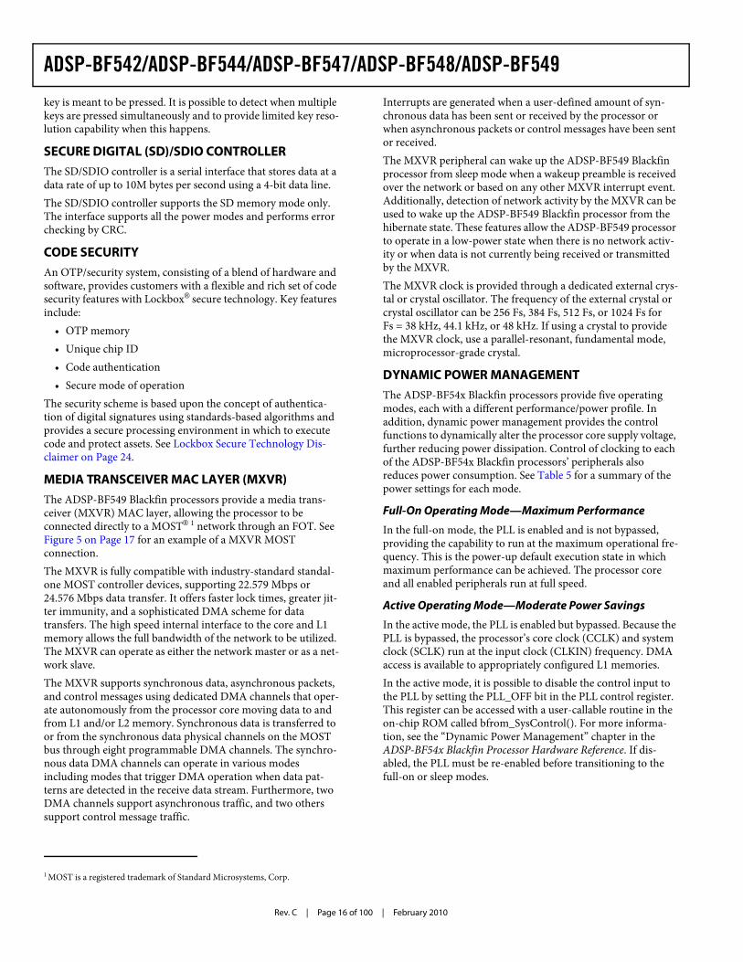
MEDIA TRANSCEIVER MAC LAYER (MXVR)The ADSP-BF549 Blackfin processors provide a media trans-ceiver (MXVR) MAC layer, allowing the processor to be connected directly to a MOST® 1 network through an FOT. See Figure 5 on Page 17 for an example of a MXVR MOST connection.The MXVR is fully compatible with industry-standard standal-one MOST controller devices, supporting 22.579 Mbps or 24.576 Mbps data transfer. It offers faster lock times, greater jit-ter immunity, and a sophisticated DMA scheme for data transfers. The high speed internal interface to the core and L1 memory allows the full bandwidth of the network to be utilized. The MXVR can operate as either the network master or as a net-work slave.The MXVR supports synchronous data, asynchronous packets, and control messages using dedicated DMA channels that oper-ate autonomously from the processor core moving data to and from L1 and/or L2 memory. Synchronous data is transferred to or from the synchronous data physical channels on the MOST bus through eight programmable DMA channels. The synchro-nous data DMA channels can operate in various modes including modes that trigger DMA operation when data pat-terns are detected in the receive data stream. Furthermore, two DMA channels support asynchronous traffic, and two others support control message traffic.
Interrupts are generated when a user-defined amount of syn-chronous data has been sent or received by the processor or when asynchronous packets or control messages have been sent or received.The MXVR peripheral can wake up the ADSP-BF549 Blackfin processor from sleep mode when a wakeup preamble is received over the network or based on any other MXVR interrupt event. Additionally, detection of network activity by the MXVR can be used to wake up the ADSP-BF549 Blackfin processor from the hibernate state. These features allow the ADSP-BF549 processor to operate in a low-power state when there is no network activ-ity or when data is not currently being received or transmitted by the MXVR.The MXVR clock is provided through a dedicated external crys-tal or crystal oscillator. The frequency of the external crystal or crystal oscillator can be 256 Fs, 384 Fs, 512 Fs, or 1024 Fs for Fs = 38 kHz, 44.1 kHz, or 48 kHz. If using a crystal to provide the MXVR clock, use a parallel-resonant, fundamental mode, microprocessor-grade crystal.
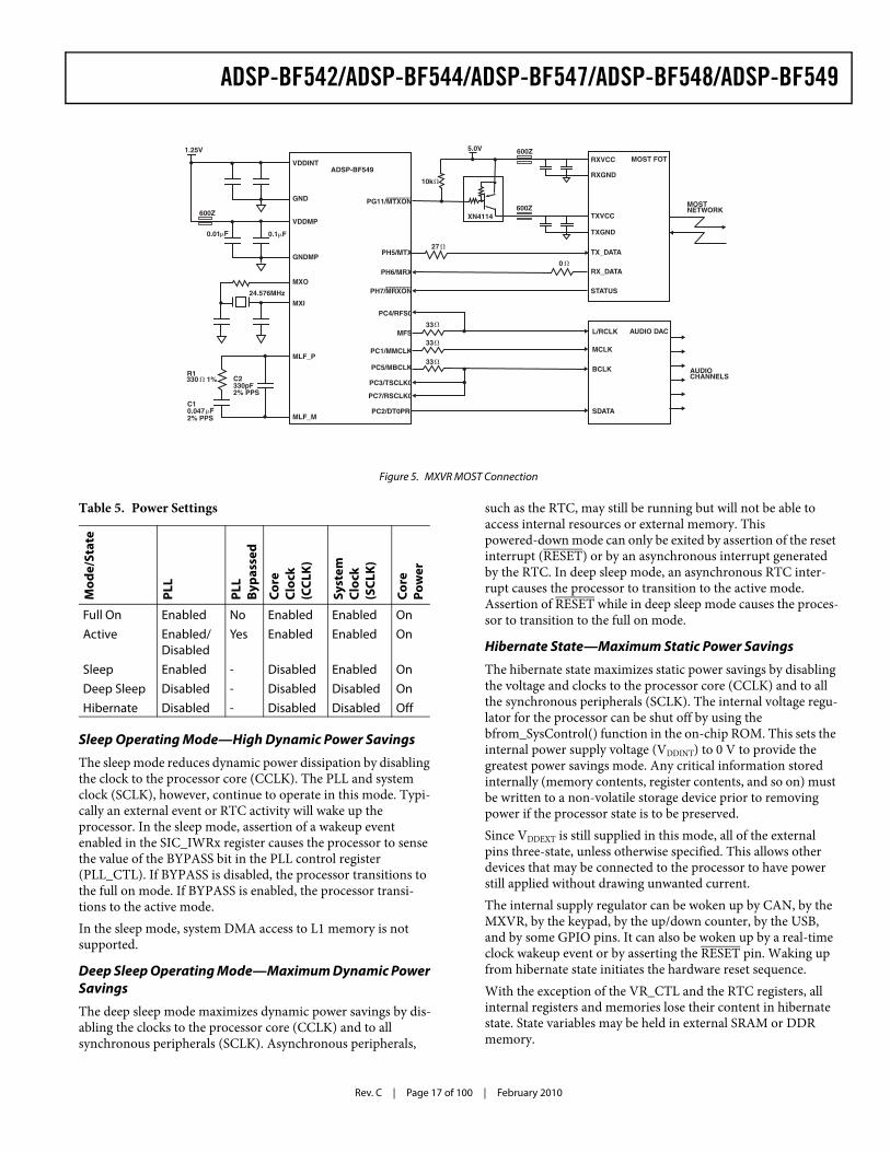
DYNAMIC POWER MANAGEMENTThe ADSP-BF54x Blackfin processors provide five operating modes, each with a different performance/power profile. In addition, dynamic power management provides the control functions to dynamically alter the processor core supply voltage, further reducing power dissipation. Control of clocking to each of the ADSP-BF54x Blackfin processors’ peripherals also reduces power consumption. See Table 5 for a summary of the power settings for each mode.
Full-On Operating Mode—Maximum Performance
In the full-on mode, the PLL is enabled and is not bypassed, providing the capability to run at the maximum operational fre-quency. This is the power-up default execution state in which maximum performance can be achieved. The processor core and all enabled peripherals run at full speed.
Active Operating Mode—Moderate Power Savings
In the active mode, the PLL is enabled but bypassed. Because the PLL is bypassed, the processor’s core clock (CCLK) and system clock (SCLK) run at the input clock (CLKIN) frequency. DMA access is available to appropriately configured L1 memories.In the active mode, it is possible to disable the control input to the PLL by setting the PLL_OFF bit in the PLL control register. This register can be accessed with a user-callable routine in the on-chip ROM called bfrom_SysControl(). For more informa-tion, see the “Dynamic Power Management” chapter in the ADSP-BF54x Blackfin Processor Hardware Reference. If dis-abled, the PLL must be re-enabled before transitioning to the full-on or sleep modes.
1 MOST is a registered trademark of Standard Microsystems, Corp.
ADSP-BF542/ADSP-BF544/ADSP-BF547/ADSP-BF548/ADSP-BF549
Rev. C | Page 17 of 100 | February 2010
Sleep Operating Mode—High Dynamic Power Savings
The sleep mode reduces dynamic power dissipation by disabling the clock to the processor core (CCLK). The PLL and system clock (SCLK), however, continue to operate in this mode. Typi-cally an external event or RTC activity will wake up the processor. In the sleep mode, assertion of a wakeup event enabled in the SIC_IWRx register causes the processor to sense the value of the BYPASS bit in the PLL control register (PLL_CTL). If BYPASS is disabled, the processor transitions to the full on mode. If BYPASS is enabled, the processor transi-tions to the active mode. In the sleep mode, system DMA access to L1 memory is not supported.
Deep Sleep Operating Mode—Maximum Dynamic Power Savings
The deep sleep mode maximizes dynamic power savings by dis-abling the clocks to the processor core (CCLK) and to all synchronous peripherals (SCLK). Asynchronous peripherals,
such as the RTC, may still be running but will not be able to access internal resources or external memory. This powered-down mode can only be exited by assertion of the reset interrupt (RESET) or by an asynchronous interrupt generated by the RTC. In deep sleep mode, an asynchronous RTC inter-rupt causes the processor to transition to the active mode. Assertion of RESET while in deep sleep mode causes the proces-sor to transition to the full on mode.
Hibernate State—Maximum Static Power Savings
The hibernate state maximizes static power savings by disabling the voltage and clocks to the processor core (CCLK) and to all the synchronous peripherals (SCLK). The internal voltage regu-lator for the processor can be shut off by using the bfrom_SysControl() function in the on-chip ROM. This sets the internal power supply voltage (VDDINT) to 0 V to provide the greatest power savings mode. Any critical information stored internally (memory contents, register contents, and so on) must be written to a non-volatile storage device prior to removing power if the processor state is to be preserved.Since VDDEXT is still supplied in this mode, all of the external pins three-state, unless otherwise specified. This allows other devices that may be connected to the processor to have power still applied without drawing unwanted current.The internal supply regulator can be woken up by CAN, by the MXVR, by the keypad, by the up/down counter, by the USB, and by some GPIO pins. It can also be woken up by a real-time clock wakeup event or by asserting the RESET pin. Waking up from hibernate state initiates the hardware reset sequence.With the exception of the VR_CTL and the RTC registers, all internal registers and memories lose their content in hibernate state. State variables may be held in external SRAM or DDR memory.
Figure 5. MXVR MOST Connection
600Z
MLF_M
MOSTNETWORK
AUDIOCHANNELS
GNDMP
VDDMP
MOST FOT
TXVCC
TX_DATA
RX_DATA
STATUS
AUDIO DAC
27
R1330
C10.047 F
0.1 F0.01 F
C2330pF
ADSP-BF549
MXI
MXO
MLF_P
PG11/MTXON
PH5/MTX
PH6/MRX
PH7/MRXON
PC1/MMCLK
MFS
PC5/MBCLK
PC3/TSCLK0
PC7/RSCLK0
PC4/RFS0
PC2/DT0PRI SDATA
L/RCLK
BCLK
MCLK
33
33
33
1.25V
GND
VDDINT
1%
2% PPS
2% PPS
0
TXGND
5.0V
RXVCC
RXGND
600Z
600Z
10k
24.576MHz
XN4114
Table 5. Power Settings
Mod
e/St
ate
PLL
PLL
Bypa
ssed
Core
Cloc
k(C
CLK
)
Syst
emCl
ock
(SCL
K)
Core
Pow
er
Full On Enabled No Enabled Enabled OnActive Enabled/
DisabledYes Enabled Enabled On
Sleep Enabled - Disabled Enabled OnDeep Sleep Disabled - Disabled Disabled OnHibernate Disabled - Disabled Disabled Off
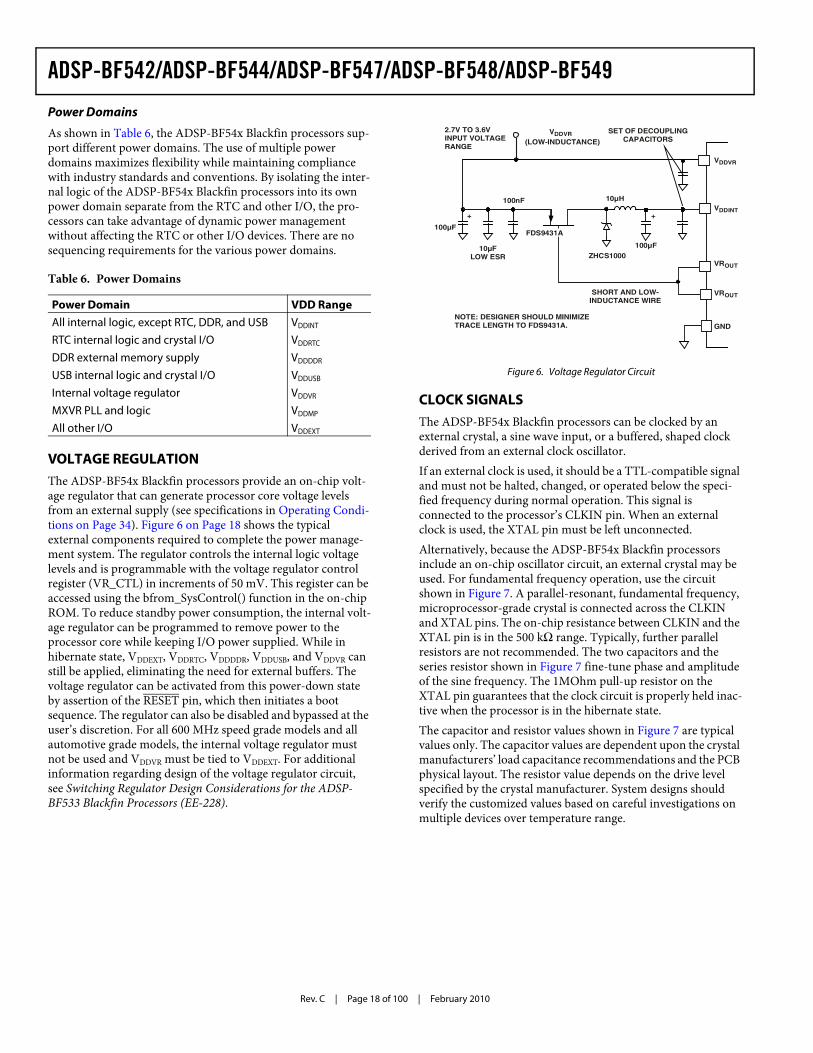
Rev. C | Page 18 of 100 | February 2010
ADSP-BF542/ADSP-BF544/ADSP-BF547/ADSP-BF548/ADSP-BF549
Power Domains
As shown in Table 6, the ADSP-BF54x Blackfin processors sup-port different power domains. The use of multiple power domains maximizes flexibility while maintaining compliance with industry standards and conventions. By isolating the inter-nal logic of the ADSP-BF54x Blackfin processors into its own power domain separate from the RTC and other I/O, the pro-cessors can take advantage of dynamic power management without affecting the RTC or other I/O devices. There are no sequencing requirements for the various power domains.
VOLTAGE REGULATIONThe ADSP-BF54x Blackfin processors provide an on-chip volt-age regulator that can generate processor core voltage levels from an external supply (see specifications in Operating Condi-tions on Page 34). Figure 6 on Page 18 shows the typical external components required to complete the power manage-ment system. The regulator controls the internal logic voltage levels and is programmable with the voltage regulator control register (VR_CTL) in increments of 50 mV. This register can be accessed using the bfrom_SysControl() function in the on-chip ROM. To reduce standby power consumption, the internal volt-age regulator can be programmed to remove power to the processor core while keeping I/O power supplied. While in hibernate state, VDDEXT, VDDRTC, VDDDDR, VDDUSB, and VDDVR can still be applied, eliminating the need for external buffers. The voltage regulator can be activated from this power-down state by assertion of the RESET pin, which then initiates a boot sequence. The regulator can also be disabled and bypassed at the user’s discretion. For all 600 MHz speed grade models and all automotive grade models, the internal voltage regulator must not be used and VDDVR must be tied to VDDEXT. For additional information regarding design of the voltage regulator circuit, see Switching Regulator Design Considerations for the ADSP-BF533 Blackfin Processors (EE-228).
CLOCK SIGNALSThe ADSP-BF54x Blackfin processors can be clocked by an external crystal, a sine wave input, or a buffered, shaped clock derived from an external clock oscillator. If an external clock is used, it should be a TTL-compatible signal and must not be halted, changed, or operated below the speci-fied frequency during normal operation. This signal is connected to the processor’s CLKIN pin. When an external clock is used, the XTAL pin must be left unconnected.Alternatively, because the ADSP-BF54x Blackfin processors include an on-chip oscillator circuit, an external crystal may be used. For fundamental frequency operation, use the circuit shown in Figure 7. A parallel-resonant, fundamental frequency, microprocessor-grade crystal is connected across the CLKIN and XTAL pins. The on-chip resistance between CLKIN and the XTAL pin is in the 500 kΩ range. Typically, further parallel resistors are not recommended. The two capacitors and the series resistor shown in Figure 7 fine-tune phase and amplitude of the sine frequency. The 1MOhm pull-up resistor on the XTAL pin guarantees that the clock circuit is properly held inac-tive when the processor is in the hibernate state.The capacitor and resistor values shown in Figure 7 are typical values only. The capacitor values are dependent upon the crystal manufacturers’ load capacitance recommendations and the PCB physical layout. The resistor value depends on the drive level specified by the crystal manufacturer. System designs should verify the customized values based on careful investigations on multiple devices over temperature range.
Table 6. Power Domains
Power Domain VDD RangeAll internal logic, except RTC, DDR, and USB VDDINT
RTC internal logic and crystal I/O VDDRTC
DDR external memory supply VDDDDR
USB internal logic and crystal I/O VDDUSB
Internal voltage regulator VDDVR
MXVR PLL and logic VDDMP
All other I/O VDDEXT
Figure 6. Voltage Regulator Circuit
VDDVR(LOW-INDUCTANCE)
VDDINT
VROUT
100μF
VROUT
GND
SHORT AND LOW-INDUCTANCE WIRE
VDDVR
+ +
100μF
10μFLOW ESR
100nF
SET OF DECOUPLINGCAPACITORS
FDS9431A
ZHCS1000
2.7V TO 3.6VINPUT VOLTAGERANGE
NOTE: DESIGNER SHOULD MINIMIZETRACE LENGTH TO FDS9431A.
10μH
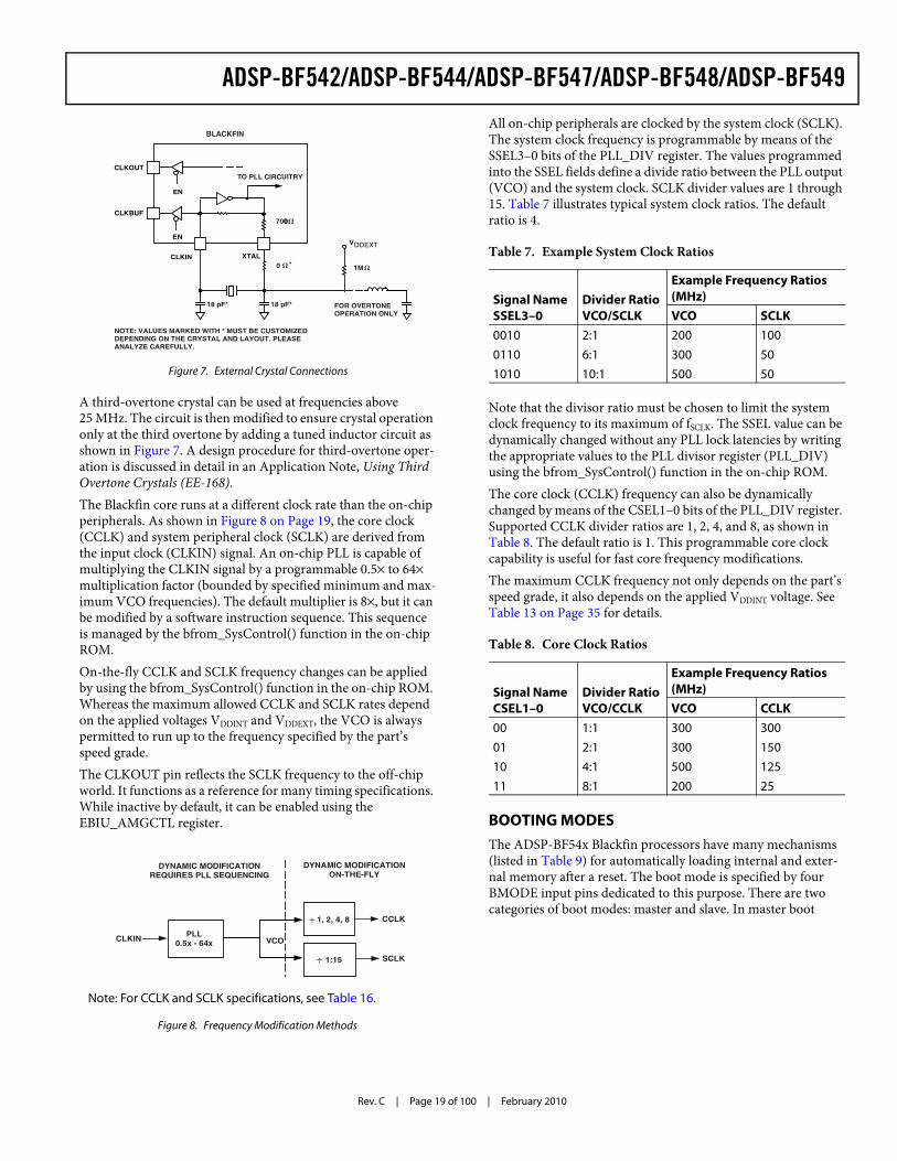
ADSP-BF542/ADSP-BF544/ADSP-BF547/ADSP-BF548/ADSP-BF549
Rev. C | Page 19 of 100 | February 2010
A third-overtone crystal can be used at frequencies above 25 MHz. The circuit is then modified to ensure crystal operation only at the third overtone by adding a tuned inductor circuit as shown in Figure 7. A design procedure for third-overtone oper-ation is discussed in detail in an Application Note, Using Third Overtone Crystals (EE-168).The Blackfin core runs at a different clock rate than the on-chip peripherals. As shown in Figure 8 on Page 19, the core clock (CCLK) and system peripheral clock (SCLK) are derived from the input clock (CLKIN) signal. An on-chip PLL is capable of multiplying the CLKIN signal by a programmable 0.5× to 64× multiplication factor (bounded by specified minimum and max-imum VCO frequencies). The default multiplier is 8×, but it can be modified by a software instruction sequence. This sequence is managed by the bfrom_SysControl() function in the on-chip ROM.On-the-fly CCLK and SCLK frequency changes can be applied by using the bfrom_SysControl() function in the on-chip ROM. Whereas the maximum allowed CCLK and SCLK rates depend on the applied voltages VDDINT and VDDEXT, the VCO is always permitted to run up to the frequency specified by the part’s speed grade. The CLKOUT pin reflects the SCLK frequency to the off-chip world. It functions as a reference for many timing specifications. While inactive by default, it can be enabled using the EBIU_AMGCTL register.
All on-chip peripherals are clocked by the system clock (SCLK). The system clock frequency is programmable by means of the SSEL3–0 bits of the PLL_DIV register. The values programmed into the SSEL fields define a divide ratio between the PLL output (VCO) and the system clock. SCLK divider values are 1 through 15. Table 7 illustrates typical system clock ratios. The default ratio is 4.
Note that the divisor ratio must be chosen to limit the system clock frequency to its maximum of fSCLK. The SSEL value can be dynamically changed without any PLL lock latencies by writing the appropriate values to the PLL divisor register (PLL_DIV) using the bfrom_SysControl() function in the on-chip ROM.The core clock (CCLK) frequency can also be dynamically changed by means of the CSEL1–0 bits of the PLL_DIV register. Supported CCLK divider ratios are 1, 2, 4, and 8, as shown in Table 8. The default ratio is 1. This programmable core clock capability is useful for fast core frequency modifications.The maximum CCLK frequency not only depends on the part’s speed grade, it also depends on the applied VDDINT voltage. See Table 13 on Page 35 for details.
BOOTING MODESThe ADSP-BF54x Blackfin processors have many mechanisms (listed in Table 9) for automatically loading internal and exter-nal memory after a reset. The boot mode is specified by four BMODE input pins dedicated to this purpose. There are two categories of boot modes: master and slave. In master boot
Figure 7. External Crystal Connections
Note: For CCLK and SCLK specifications, see Table 16.
Figure 8. Frequency Modification Methods
CLKIN
CLKOUT
XTAL
EN
CLKBUF
TO PLL CIRCUITRY
F R OVERTONEOPERA
OTION ONLY
NOTE: VALUES MARKED WITH * MUST BE CUSTOMIZEDDEPENDING ON THE CRYSTAL AND LAYOUT. PLEASEANALYZE CAREFULLY.
18 pF*
EN
18 pF*
7000
BLACKFIN
0 *
VDDEXT
1M
PLL0.5x - 64x
1:15
1, 2, 4, 8
VCOCLKIN
DYNAMIC MODIFICATIONREQUIRES PLL SEQUENCING
DYNAMIC MODIFICATIONON-THE-FLY
CCLK
SCLK
Table 7. Example System Clock Ratios
Signal Name SSEL3–0
Divider Ratio VCO/SCLK
Example Frequency Ratios (MHz)VCO SCLK
0010 2:1 200 1000110 6:1 300 501010 10:1 500 50
Table 8. Core Clock Ratios
Signal Name CSEL1–0
Divider Ratio VCO/CCLK
Example Frequency Ratios (MHz)VCO CCLK
00 1:1 300 30001 2:1 300 15010 4:1 500 12511 8:1 200 25
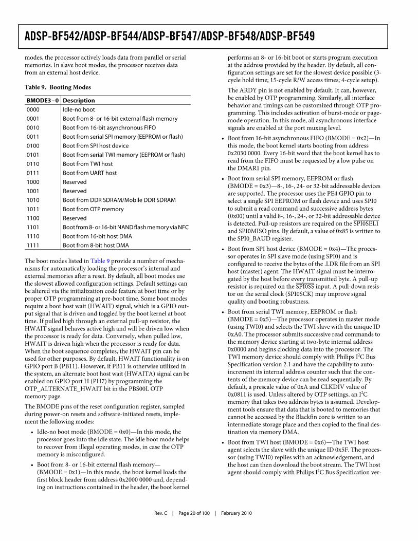
Rev. C | Page 20 of 100 | February 2010
ADSP-BF542/ADSP-BF544/ADSP-BF547/ADSP-BF548/ADSP-BF549
modes, the processor actively loads data from parallel or serial memories. In slave boot modes, the processor receives data from an external host device.
The boot modes listed in Table 9 provide a number of mecha-nisms for automatically loading the processor’s internal and external memories after a reset. By default, all boot modes use the slowest allowed configuration settings. Default settings can be altered via the initialization code feature at boot time or by proper OTP programming at pre-boot time. Some boot modes require a boot host wait (HWAIT) signal, which is a GPIO out-put signal that is driven and toggled by the boot kernel at boot time. If pulled high through an external pull-up resistor, the HWAIT signal behaves active high and will be driven low when the processor is ready for data. Conversely, when pulled low, HWAIT is driven high when the processor is ready for data. When the boot sequence completes, the HWAIT pin can be used for other purposes. By default, HWAIT functionality is on GPIO port B (PB11). However, if PB11 is otherwise utilized in the system, an alternate boot host wait (HWAITA) signal can be enabled on GPIO port H (PH7) by programming the OTP_ALTERNATE_HWAIT bit in the PBS00L OTP memory page.The BMODE pins of the reset configuration register, sampled during power-on resets and software-initiated resets, imple-ment the following modes:
• Idle-no boot mode (BMODE = 0x0)—In this mode, the processor goes into the idle state. The idle boot mode helps to recover from illegal operating modes, in case the OTP memory is misconfigured.
• Boot from 8- or 16-bit external flash memory— (BMODE = 0x1)—In this mode, the boot kernel loads the first block header from address 0x2000 0000 and, depend-ing on instructions contained in the header, the boot kernel
performs an 8- or 16-bit boot or starts program execution at the address provided by the header. By default, all con-figuration settings are set for the slowest device possible (3-cycle hold time; 15-cycle R/W access times; 4-cycle setup). The ARDY pin is not enabled by default. It can, however, be enabled by OTP programming. Similarly, all interface behavior and timings can be customized through OTP pro-gramming. This includes activation of burst-mode or page-mode operation. In this mode, all asynchronous interface signals are enabled at the port muxing level.
• Boot from 16-bit asynchronous FIFO (BMODE = 0x2)—In this mode, the boot kernel starts booting from address 0x2030 0000. Every 16-bit word that the boot kernel has to read from the FIFO must be requested by a low pulse on the DMAR1 pin.
• Boot from serial SPI memory, EEPROM or flash (BMODE = 0x3)—8-, 16-, 24- or 32-bit addressable devices are supported. The processor uses the PE4 GPIO pin to select a single SPI EEPROM or flash device and uses SPI0 to submit a read command and successive address bytes (0x00) until a valid 8-, 16-, 24-, or 32-bit addressable device is detected. Pull-up resistors are required on the SPI0SEL1 and SPI0MISO pins. By default, a value of 0x85 is written to the SPI0_BAUD register.
• Boot from SPI host device (BMODE = 0x4)—The proces-sor operates in SPI slave mode (using SPI0) and is configured to receive the bytes of the .LDR file from an SPI host (master) agent. The HWAIT signal must be interro-gated by the host before every transmitted byte. A pull-up resistor is required on the SPI0SS input. A pull-down resis-tor on the serial clock (SPI0SCK) may improve signal quality and booting robustness.
• Boot from serial TWI memory, EEPROM or flash (BMODE = 0x5)—The processor operates in master mode (using TWI0) and selects the TWI slave with the unique ID 0xA0. The processor submits successive read commands to the memory device starting at two-byte internal address 0x0000 and begins clocking data into the processor. The TWI memory device should comply with Philips I2C Bus Specification version 2.1 and have the capability to auto-increment its internal address counter such that the con-tents of the memory device can be read sequentially. By default, a prescale value of 0xA and CLKDIV value of 0x0811 is used. Unless altered by OTP settings, an I2C memory that takes two address bytes is assumed. Develop-ment tools ensure that data that is booted to memories that cannot be accessed by the Blackfin core is written to an intermediate storage place and then copied to the final des-tination via memory DMA.
• Boot from TWI host (BMODE = 0x6)—The TWI host agent selects the slave with the unique ID 0x5F. The proces-sor (using TWI0) replies with an acknowledgement, and the host can then download the boot stream. The TWI host agent should comply with Philips I2C Bus Specification ver-
Table 9. Booting Modes
BMODE3–0 Description0000 Idle-no boot0001 Boot from 8- or 16-bit external flash memory0010 Boot from 16-bit asynchronous FIFO0011 Boot from serial SPI memory (EEPROM or flash)0100 Boot from SPI host device0101 Boot from serial TWI memory (EEPROM or flash)0110 Boot from TWI host0111 Boot from UART host1000 Reserved1001 Reserved1010 Boot from DDR SDRAM/Mobile DDR SDRAM1011 Boot from OTP memory1100 Reserved1101 Boot from 8- or 16-bit NAND flash memory via NFC1110 Boot from 16-bit host DMA1111 Boot from 8-bit host DMA
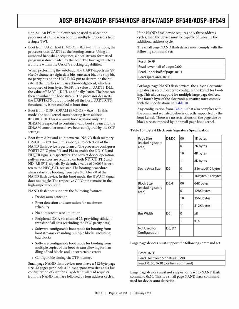
ADSP-BF542/ADSP-BF544/ADSP-BF547/ADSP-BF548/ADSP-BF549
Rev. C | Page 21 of 100 | February 2010
sion 2.1. An I2C multiplexer can be used to select one processor at a time when booting multiple processors from a single TWI.
• Boot from UART host (BMODE = 0x7)—In this mode, the processor uses UART1 as the booting source. Using an autobaud handshake sequence, a boot-stream-formatted program is downloaded by the host. The host agent selects a bit rate within the UART’s clocking capabilities.When performing the autobaud, the UART expects an “@” (0x40) character (eight data bits, one start bit, one stop bit, no parity bit) on the UART1RX pin to determine the bit rate. It then replies with an acknowledgement, which is composed of four bytes (0xBF, the value of UART1_DLL, the value of UART1_DLH, and finally 0x00). The host can then download the boot stream. The processor deasserts the UART1RTS output to hold off the host; UART1CTS functionality is not enabled at boot time.
• Boot from (DDR) SDRAM (BMODE = 0xA)—In this mode, the boot kernel starts booting from address 0x0000 0010. This is a warm boot scenario only. The SDRAM is expected to contain a valid boot stream and the SDRAM controller must have been configured by the OTP settings.
• Boot from 8-bit and 16-bit external NAND flash memory (BMODE = 0xD)—In this mode, auto detection of the NAND flash device is performed. The processor configures PORTJ GPIO pins PJ1 and PJ2 to enable the ND_CE and ND_RB signals, respectively. For correct device operation, pull-up resistors are required on both ND_CE (PJ1) and ND_RB (PJ2) signals. By default, a value of 0x0033 is writ-ten to the NFC_CTL register. The booting procedure always starts by booting from byte 0 of block 0 of the NAND flash device. In this boot mode, the HWAIT signal does not toggle. The respective GPIO pin remains in the high-impedance state.NAND flash boot supports the following features:
• Device auto detection• Error detection and correction for maximum
reliability• No boot stream size limitation• Peripheral DMA via channel 22, providing efficient
transfer of all data (excluding the ECC parity data)• Software-configurable boot mode for booting from
boot streams expanding multiple blocks, including bad blocks
• Software-configurable boot mode for booting from multiple copies of the boot stream allowing for han-dling of bad blocks and uncorrectable errors
• Configurable timing via OTP memorySmall page NAND flash devices must have a 512-byte page size, 32 pages per block, a 16-byte spare area size and a bus configuration of eight bits. By default, all read requests from the NAND flash are followed by four address cycles.
If the NAND flash device requires only three address cycles, then the device must be capable of ignoring the additional address cycle.The small page NAND flash device must comply with the following command set:
For large page NAND flash devices, the 4-byte electronic signature is read in order to configure the kernel for boot-ing. This allows support for multiple large page devices. The fourth byte of the electronic signature must comply with the specifications in Table 10.Any configuration from Table 10 that also complies with the command set listed below is directly supported by the boot kernel. There are no restrictions on the page size or block size as imposed by the small-page boot kernel.
Large page devices must support the following command set:
Large page devices must not support or react to NAND flash command 0x50. This is a small page NAND flash command used for device auto detection.
Reset: 0xFFRead lower half of page: 0x00Read upper half of page: 0x01Read spare area: 0x50
Table 10. Byte 4 Electronic Signature Specification
Page Size (excluding spare area)
D1:D0 00 1K bytes
01 2K bytes
10 4K bytes
11 8K bytes
Spare Area Size D2 0 8 bytes/512 bytes
1 16 bytes/512 bytes
Block Size (excluding spare area)
D5:4 00 64K bytes
01 128K bytes
10 256K bytes
11 512K bytes
Bus Width D6 0 x8
1 x16
Not Used for Configuration
D3, D7
Reset: 0xFFRead Electronic Signature: 0x90Read: 0x00, 0x30 (confirm command)
Rev. C | Page 22 of 100 | February 2010
ADSP-BF542/ADSP-BF544/ADSP-BF547/ADSP-BF548/ADSP-BF549
By default, the boot kernel will always issue five address cycles; therefore, if a large page device requires only four cycles, the device must be capable of ignoring the additional address cycle.16-bit NAND flash memory devices must only support the issu-ing of command and address cycles via the lower eight bits of the data bus. Devices that use the full 16-bit bus for command and address cycles are not supported.
• Boot from OTP memory (BMODE = 0xB)—This provides a standalone booting method. The boot stream is loaded from on-chip OTP memory. By default, the boot stream is expected to start from OTP page 0x40 and can occupy all public OTP memory up to page 0xDF (2560 bytes). Since the start page is programmable, the maximum size of the boot stream can be extended to 3072 bytes.
• Boot from 16-bit host DMA (BMODE = 0xE)—In this mode, the host DMA port is configured in 16-bit acknowl-edge mode with little endian data format. Unlike other modes, the host is responsible for interpreting the boot stream. It writes data blocks individually into the host DMA port. Before configuring the DMA settings for each block, the host may either poll the ALLOW_CONFIG bit in HOST_STATUS or wait to be interrupted by the HWAIT signal. When using HWAIT, the host must still check ALLOW_CONFIG at least once before beginning to con-figure the host DMA port. After completing the configuration, the host is required to poll the READY bit in HOST_STATUS before beginning to transfer data. When the host sends an HIRQ control command, the boot kernel issues a CALL instruction to address 0xFFA0 0000. It is the host’s responsibility to ensure valid code has been placed at this address. The routine at address 0xFFA0 0000 can be a simple initialization routine to configure internal resources, such as the SDRAM controller, which then returns using an RTS instruction. The routine may also be the final application, which will never return to the boot kernel.
• Boot from 8-bit host DMA (BMODE = 0xF)—In this mode, the host DMA port is configured in 8-bit interrupt mode with little endian data format. Unlike other modes, the host is responsible for interpreting the boot stream. It writes data blocks individually to the host DMA port. Before configuring the DMA settings for each block, the host may either poll the ALLOW_CONFIG bit in HOST_STATUS or wait to be interrupted by the HWAIT signal. When using HWAIT, the host must still check ALLOW_CONFIG at least once before beginning to con-figure the host DMA port. The host will receive an interrupt from the HOST_ACK signal every time it is allowed to send the next FIFO depth’s worth (sixteen 32-bit words) of information. When the host sends an HIRQ con-trol command, the boot kernel issues a CALL instruction to address 0xFFA0 0000. It is the host's responsibility to ensure valid code has been placed at this address. The rou-tine at address 0xFFA0 0000 can be a simple initialization routine to configure internal resources, such as the
SDRAM controller, which then returns using an RTS instruction. The routine may also be the final application, which will never return to the boot kernel.
For each of the boot modes, a 16-byte header is first read from an external memory device. The header specifies the number of bytes to be transferred and the memory destination address. Multiple memory blocks may be loaded by any boot sequence. Once all blocks are loaded, program execution commences from the address stored in the EVT1 register.Prior to booting, the pre-boot routine interrogates the OTP memory. Individual boot modes can be customized or disabled based on OTP programming. External hardware, especially booting hosts, may monitor the HWAIT signal to determine when the pre-boot has finished and the boot kernel starts the boot process. However, the HWAIT signal does not toggle in NAND boot mode. By programming OTP memory, the user can instruct the preboot routine to also customize the PLL, volt-age regulator, DDR controller, and/or asynchronous memory interface controller.The boot kernel differentiates between a regular hardware reset and a wakeup-from-hibernate event to speed up booting in the later case. Bits 6-4 in the system reset configuration (SYSCR) register can be used to bypass the pre-boot routine and/or boot kernel in case of a software reset. They can also be used to simu-late a wakeup-from-hibernate boot in the software reset case.The boot process can be further customized by “initialization code.” This is a piece of code that is loaded and executed prior to the regular application boot. Typically, this is used to configure the DDR controller or to speed up booting by managing PLL, clock frequencies, wait states, and/or serial bit rates.The boot ROM also features C-callable function entries that can be called by the user application at run time. This enables sec-ond-stage boot or booting management schemes to be implemented with ease.
INSTRUCTION SET DESCRIPTIONThe Blackfin processor family assembly language instruction set employs an algebraic syntax designed for ease of coding and readability. The instructions have been specifically tuned to pro-vide a flexible, densely encoded instruction set that compiles to a very small final memory size. The instruction set also provides fully featured multifunction instructions that allow the pro-grammer to use many of the processor core resources in a single instruction. Coupled with many features more often seen on microcontrollers, this instruction set is very efficient when com-piling C and C++ source code. In addition, the architecture supports both user (algorithm/application code) and supervisor (O/S kernel, device drivers, debuggers, ISRs) modes of opera-tion, allowing multiple levels of access to core processor resources.
ADSP-BF542/ADSP-BF544/ADSP-BF547/ADSP-BF548/ADSP-BF549
Rev. C | Page 23 of 100 | February 2010
The assembly language, which takes advantage of the proces-sor’s unique architecture, offers the following advantages:
• Seamlessly integrated DSP/MCU features are optimized for both 8-bit and 16-bit operations.
• A multi-issue load/store modified-Harvard architecture, which supports two 16-bit MAC or four 8-bit ALU + two load/store + two pointer updates per cycle.
• All registers, I/O, and memory are mapped into a unified 4G byte memory space, providing a simplified program-ming model.
• Microcontroller features, such as arbitrary bit and bit-field manipulation, insertion, and extraction; integer operations on 8-, 16-, and 32-bit data-types; and separate user and supervisor stack pointers.
• Code density enhancements, which include intermixing of 16- and 32-bit instructions (no mode switching, no code segregation). Frequently used instructions are encoded in 16 bits.
DEVELOPMENT TOOLSThe ADSP-BF54x Blackfin processors are supported with a complete set of CROSSCORE® software and hardware develop-ment tools, including Analog Devices emulators and VisualDSP++® development environment. The same emulator hardware that supports other Blackfin processors also fully emulates the ADSP-BF54x Blackfin processors.
EZ-KIT Lite Evaluation Board
For evaluation of ADSP-BF54x Blackfin processors, use the ADSP-BF548 EZ-KIT Lite® board available from Analog Devices. Order part number ADZS-BF548-EZLITE. The board comes with on-chip emulation capabilities and is equipped to enable software development. Multiple daughter cards are available.
DESIGNING AN EMULATOR-COMPATIBLE PROCESSOR BOARDThe Analog Devices family of emulators are tools that every sys-tem developer needs to test and debug hardware and software systems. Analog Devices has supplied an IEEE 1149.1 JTAG test access port (TAP) on each JTAG processor. The emulator uses the TAP to access the internal features of the processor, allow-ing the developer to load code, set breakpoints, observe variables, observe memory, and examine registers. The proces-sor must be halted to send data and commands, but once an operation has been completed by the emulator, the processor is set running at full speed with no impact on system timing.To use these emulators, the target board must include a header that connects the processor’s JTAG port to the emulator.For details on target board design issues including mechanical layout, single processor connections, multiprocessor scan chains, signal buffering, signal termination, and emulator pod logic, see Analog Devices JTAG Emulation Technical Reference
(EE-68) on the Analog Devices web site under www.analog.com/ee-notes. This document is updated regularly to keep pace with improvements to emulator support.
MXVR BOARD LAYOUT GUIDELINESThe MXVR Loop Filter RC network is connected between the MLF_P and MLF_M pins in the following manner:Capacitors:
• C1: 0.047 µF (PPS type, 2% tolerance recommended)• C2: 330 pF (PPS type, 2% tolerance recommended)
Resistor: • R1: 330 Ω (1% tolerance)
The RC network should be located physically close to the MLF_P and MLF_M pins on the board.The RC network should be shielded using GNDMP traces.Avoid routing other switching signals near the RC network to avoid crosstalk.MXI driven with external clock oscillator IC:
• MXI should be driven with the clock output of a clock oscillator IC running at a frequency of 49.152 MHz or 45.1584 MHz.
• MXO should be left unconnected.• Avoid routing other switching signals near the oscillator
and clock output trace to avoid crosstalk. When not possi-ble, shield traces with ground.
MXI/MXO with external crystal:• The crystal must be a fundamental mode crystal running at
a frequency of 49.152 MHz or 45.1584 MHz.• The crystal and load capacitors should be placed physically
close to the MXI and MXO pins on the board.• Board trace capacitance on each lead should not be more
than 3 pF.• Trace capacitance plus load capacitance should equal the
load capacitance specification for the crystal.• Avoid routing other switching signals near the crystal and
components to avoid crosstalk. When not possible, shield traces and components with ground.
VDDMP/GNDMP—MXVR PLL power domain:• Route VDDMP and GNDMP with wide traces or as isolated
power planes.• Drive VDDMP to same level as VDDINT.• Place a ferrite bead between the VDDINT power plane and the
VDDMP pin for noise isolation.• Locally bypass VDDMP with 0.1 µF and 0.01 µF decoupling
capacitors to GNDMP.• Avoid routing switching signals near to VDDMP and GNDMP
traces to avoid crosstalk.
Rev. C | Page 24 of 100 | February 2010
ADSP-BF542/ADSP-BF544/ADSP-BF547/ADSP-BF548/ADSP-BF549
Fiber optic transceiver (FOT) connections:• Keep the traces between the ADSP-BF549 processor and
the FOT as short as possible.• The receive data trace connecting the FOT receive data
output pin to the ADSP-BF549 PH6/MRX input pin should have a 0 Ω series termination resistor placed close to the FOT receive data output pin. Typically, the edge rate of the FOT receive data signal driven by the FOT is very slow, and further degradation of the edge rate is not desirable.
• The transmit data trace connecting the ADSP-BF549 PH5/MTX output pin to the FOT transmit data input pin should have a 27 Ω series termination resistor placed close to the ADSP-BF549 PH5/MTX pin.
• The receive data trace and the transmit data trace between the ADSP-BF549 processor and the FOT should not be routed close to each other in parallel over long distances to avoid crosstalk.
RELATED DOCUMENTSThe following publications that describe the ADSP-BF54x Blackfin processors (and related processors) can be ordered from any Analog Devices sales office or accessed electronically on www.analog.com:
• ADSP-BF54x Blackfin Processor Hardware Reference, Vol-ume 1 and Volume 2
• Blackfin Processor Programming Reference• ADSP-BF542/BF544/BF547/BF548/BF549
Blackfin Anomaly List
LOCKBOX SECURE TECHNOLOGY DISCLAIMERAnalog Devices products containing Lockbox Secure Technol-ogy are warranted by Analog Devices as detailed in the Analog Devices Standard Terms and Conditions of Sale. To our knowl-edge, the Lockbox secure technology, when used in accordance with the data sheet and hardware reference manual specifica-tions, provides a secure method of implementing code and data safeguards. However, Analog Devices does not guarantee that this technology provides absolute security. ACCORDINGLY, ANALOG DEVICES HEREBY DISCLAIMS ANY AND ALL EXPRESS AND IMPLIED WARRANTIES THAT THE LOCK-BOX SECURE TECHNOLOGY CANNOT BE BREACHED, COMPROMISED, OR OTHERWISE CIRCUMVENTED AND IN NO EVENT SHALL ANALOG DEVICES BE LIABLE FOR ANY LOSS, DAMAGE, DESTRUCTION, OR RELEASE OF DATA, INFORMATION, PHYSICAL PROPERTY, OR INTEL-LECTUAL PROPERTY.
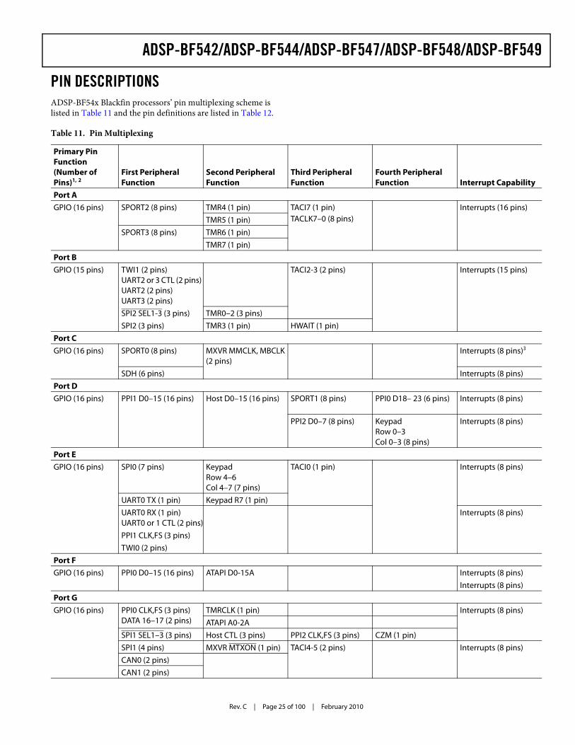
ADSP-BF542/ADSP-BF544/ADSP-BF547/ADSP-BF548/ADSP-BF549
Rev. C | Page 25 of 100 | February 2010
PIN DESCRIPTIONSADSP-BF54x Blackfin processors’ pin multiplexing scheme is listed in Table 11 and the pin definitions are listed in Table 12.
Table 11. Pin Multiplexing
Primary Pin Function(Number of Pins)1, 2
First Peripheral Function
Second Peripheral Function
Third Peripheral Function
Fourth Peripheral Function Interrupt Capability
Port AGPIO (16 pins) SPORT2 (8 pins) TMR4 (1 pin) TACI7 (1 pin)
TACLK7–0 (8 pins)Interrupts (16 pins)
TMR5 (1 pin)SPORT3 (8 pins) TMR6 (1 pin)
TMR7 (1 pin)Port BGPIO (15 pins) TWI1 (2 pins)
UART2 or 3 CTL (2 pins) UART2 (2 pins) UART3 (2 pins)
TACI2-3 (2 pins) Interrupts (15 pins)
SPI2 SEL1-3 (3 pins) TMR0–2 (3 pins)SPI2 (3 pins) TMR3 (1 pin) HWAIT (1 pin)
Port CGPIO (16 pins) SPORT0 (8 pins) MXVR MMCLK, MBCLK
(2 pins)Interrupts (8 pins)3
SDH (6 pins) Interrupts (8 pins)Port DGPIO (16 pins) PPI1 D0–15 (16 pins) Host D0–15 (16 pins) SPORT1 (8 pins) PPI0 D18– 23 (6 pins) Interrupts (8 pins)
PPI2 D0–7 (8 pins) KeypadRow 0–3Col 0–3 (8 pins)
Interrupts (8 pins)
Port EGPIO (16 pins) SPI0 (7 pins) Keypad
Row 4–6 Col 4–7 (7 pins)
TACI0 (1 pin) Interrupts (8 pins)
UART0 TX (1 pin) Keypad R7 (1 pin)UART0 RX (1 pin) UART0 or 1 CTL (2 pins)
Interrupts (8 pins)
PPI1 CLK,FS (3 pins)TWI0 (2 pins)
Port FGPIO (16 pins) PPI0 D0–15 (16 pins) ATAPI D0-15A Interrupts (8 pins)
Interrupts (8 pins)Port GGPIO (16 pins) PPI0 CLK,FS (3 pins)
DATA 16–17 (2 pins)TMRCLK (1 pin) Interrupts (8 pins)ATAPI A0-2A
SPI1 SEL1–3 (3 pins) Host CTL (3 pins) PPI2 CLK,FS (3 pins) CZM (1 pin)SPI1 (4 pins) MXVR MTXON (1 pin) TACI4-5 (2 pins) Interrupts (8 pins)CAN0 (2 pins) CAN1 (2 pins)
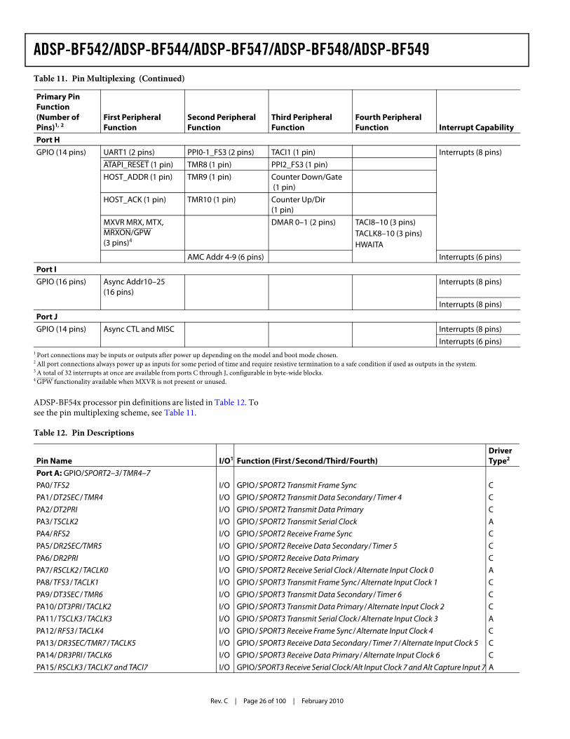
Rev. C | Page 26 of 100 | February 2010
ADSP-BF542/ADSP-BF544/ADSP-BF547/ADSP-BF548/ADSP-BF549
ADSP-BF54x processor pin definitions are listed in Table 12. To see the pin multiplexing scheme, see Table 11.
Port HGPIO (14 pins) UART1 (2 pins) PPI0-1_FS3 (2 pins) TACI1 (1 pin) Interrupts (8 pins)
ATAPI_RESET (1 pin) TMR8 (1 pin) PPI2_FS3 (1 pin)HOST_ADDR (1 pin) TMR9 (1 pin) Counter Down/Gate
(1 pin) HOST_ACK (1 pin) TMR10 (1 pin) Counter Up/Dir
(1 pin)
MXVR MRX, MTX, MRXON/GPW (3 pins)4
DMAR 0–1 (2 pins) TACI8–10 (3 pins)TACLK8–10 (3 pins)HWAITA
AMC Addr 4-9 (6 pins) Interrupts (6 pins)Port IGPIO (16 pins) Async Addr10–25
(16 pins)Interrupts (8 pins)
Interrupts (8 pins)Port JGPIO (14 pins) Async CTL and MISC Interrupts (8 pins)
Interrupts (6 pins)1 Port connections may be inputs or outputs after power up depending on the model and boot mode chosen.2 All port connections always power up as inputs for some period of time and require resistive termination to a safe condition if used as outputs in the system.3 A total of 32 interrupts at once are available from ports C through J, configurable in byte-wide blocks.4 GPW functionality available when MXVR is not present or unused.
Table 11. Pin Multiplexing (Continued)
Primary Pin Function(Number of Pins)1, 2
First Peripheral Function
Second Peripheral Function
Third Peripheral Function
Fourth Peripheral Function Interrupt Capability
Table 12. Pin Descriptions
Pin Name I/O1 Function (First/Second/Third/Fourth)Driver Type2
Port A: GPIO/SPORT2–3/TMR4–7PA0/TFS2 I/O GPIO/SPORT2 Transmit Frame Sync CPA1/DT2SEC/TMR4 I/O GPIO/SPORT2 Transmit Data Secondary/Timer 4 CPA2/DT2PRI I/O GPIO/SPORT2 Transmit Data Primary CPA3/TSCLK2 I/O GPIO/SPORT2 Transmit Serial Clock APA4/RFS2 I/O GPIO/SPORT2 Receive Frame Sync CPA5/DR2SEC/TMR5 I/O GPIO/SPORT2 Receive Data Secondary/Timer 5 CPA6/DR2PRI I/O GPIO/SPORT2 Receive Data Primary CPA7/RSCLK2/TACLK0 I/O GPIO/SPORT2 Receive Serial Clock/Alternate Input Clock 0 APA8/TFS3/TACLK1 I/O GPIO/SPORT3 Transmit Frame Sync/Alternate Input Clock 1 CPA9/DT3SEC/TMR6 I/O GPIO/SPORT3 Transmit Data Secondary/Timer 6 CPA10/DT3PRI/TACLK2 I/O GPIO/SPORT3 Transmit Data Primary/Alternate Input Clock 2 CPA11/TSCLK3/TACLK3 I/O GPIO/SPORT3 Transmit Serial Clock/Alternate Input Clock 3 APA12/RFS3/TACLK4 I/O GPIO/SPORT3 Receive Frame Sync/Alternate Input Clock 4 CPA13/DR3SEC/TMR7/TACLK5 I/O GPIO/SPORT3 Receive Data Secondary/Timer 7/Alternate Input Clock 5 CPA14/DR3PRI/TACLK6 I/O GPIO/SPORT3 Receive Data Primary/Alternate Input Clock 6 CPA15/RSCLK3/TACLK7 and TACI7 I/O GPIO/SPORT3 Receive Serial Clock/Alt Input Clock 7 and Alt Capture Input 7 A
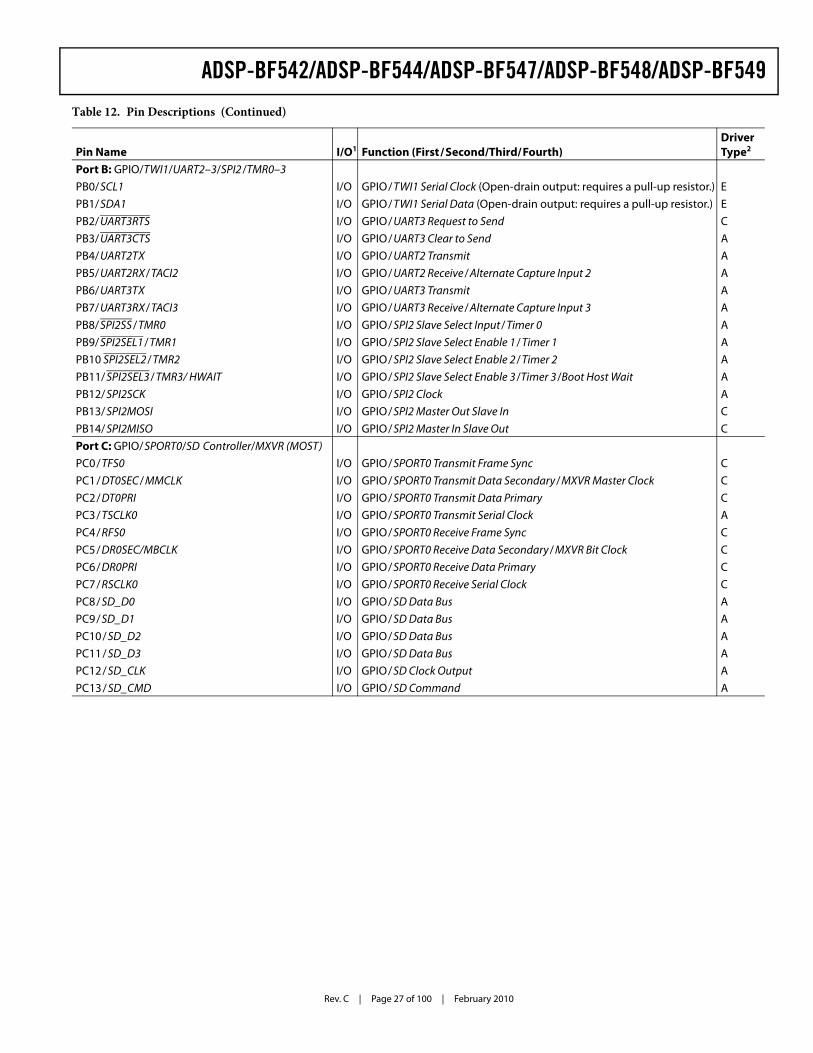
ADSP-BF542/ADSP-BF544/ADSP-BF547/ADSP-BF548/ADSP-BF549
Rev. C | Page 27 of 100 | February 2010
Port B: GPIO/TWI1/UART2–3/SPI2/TMR0–3PB0/SCL1 I/O GPIO/TWI1 Serial Clock (Open-drain output: requires a pull-up resistor.) EPB1/SDA1 I/O GPIO/TWI1 Serial Data (Open-drain output: requires a pull-up resistor.) EPB2/UART3RTS I/O GPIO/UART3 Request to Send CPB3/UART3CTS I/O GPIO/UART3 Clear to Send APB4/UART2TX I/O GPIO/UART2 Transmit APB5/UART2RX/TACI2 I/O GPIO/UART2 Receive/Alternate Capture Input 2 APB6/UART3TX I/O GPIO/UART3 Transmit APB7/UART3RX/TACI3 I/O GPIO/UART3 Receive/Alternate Capture Input 3 APB8/SPI2SS /TMR0 I/O GPIO/SPI2 Slave Select Input/Timer 0 APB9/SPI2SEL1/TMR1 I/O GPIO/SPI2 Slave Select Enable 1/Timer 1 APB10 SPI2SEL2/TMR2 I/O GPIO/SPI2 Slave Select Enable 2/Timer 2 APB11/SPI2SEL3/TMR3/ HWAIT I/O GPIO/SPI2 Slave Select Enable 3/Timer 3/Boot Host Wait APB12/SPI2SCK I/O GPIO/SPI2 Clock APB13/SPI2MOSI I/O GPIO/SPI2 Master Out Slave In CPB14/SPI2MISO I/O GPIO/SPI2 Master In Slave Out CPort C: GPIO/SPORT0/SD Controller/MXVR (MOST)PC0/TFS0 I/O GPIO/SPORT0 Transmit Frame Sync CPC1/DT0SEC/MMCLK I/O GPIO/SPORT0 Transmit Data Secondary/MXVR Master Clock CPC2/DT0PRI I/O GPIO/SPORT0 Transmit Data Primary CPC3/TSCLK0 I/O GPIO/SPORT0 Transmit Serial Clock APC4/RFS0 I/O GPIO/SPORT0 Receive Frame Sync CPC5/DR0SEC/MBCLK I/O GPIO/SPORT0 Receive Data Secondary/MXVR Bit Clock CPC6/DR0PRI I/O GPIO/SPORT0 Receive Data Primary CPC7/RSCLK0 I/O GPIO/SPORT0 Receive Serial Clock CPC8/SD_D0 I/O GPIO/SD Data Bus APC9/SD_D1 I/O GPIO/SD Data Bus APC10/SD_D2 I/O GPIO/SD Data Bus APC11/SD_D3 I/O GPIO/SD Data Bus APC12/SD_CLK I/O GPIO/SD Clock Output APC13/SD_CMD I/O GPIO/SD Command A
Table 12. Pin Descriptions (Continued)
Pin Name I/O1 Function (First/Second/Third/Fourth)Driver Type2
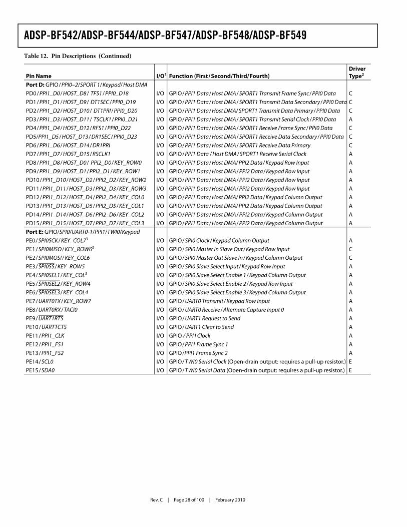
Rev. C | Page 28 of 100 | February 2010
ADSP-BF542/ADSP-BF544/ADSP-BF547/ADSP-BF548/ADSP-BF549
Port D: GPIO/PPI0–2/SPORT 1/Keypad/Host DMA PD0/PPI1_D0/HOST_D8/ TFS1/PPI0_D18 I/O GPIO/PPI1 Data/Host DMA/SPORT1 Transmit Frame Sync/PPI0 Data CPD1/PPI1_D1/HOST_D9/ DT1SEC/PPI0_D19 I/O GPIO/PPI1 Data/Host DMA/SPORT1 Transmit Data Secondary/PPI0 Data CPD2/PPI1_D2/HOST_D10/ DT1PRI/PPI0_D20 I/O GPIO/PPI1 Data/Host DMA/SPORT1 Transmit Data Primary/PPI0 Data CPD3/PPI1_D3/HOST_D11/ TSCLK1/PPI0_D21 I/O GPIO/PPI1 Data/Host DMA/SPORT1 Transmit Serial Clock/PPI0 Data APD4/PPI1_D4/HOST_D12/RFS1/PPI0_D22 I/O GPIO/PPI1 Data/Host DMA/SPORT1 Receive Frame Sync/PPI0 Data CPD5/PPI1_D5/HOST_D13/DR1SEC/PPI0_D23 I/O GPIO/PPI1 Data/Host DMA/SPORT1 Receive Data Secondary/PPI0 Data CPD6/PPI1_D6/HOST_D14/DR1PRI I/O GPIO/PPI1 Data/Host DMA/SPORT1 Receive Data Primary CPD7/PPI1_D7/HOST_D15/RSCLK1 I/O GPIO/PPI1 Data /Host DMA/SPORT1 Receive Serial Clock APD8/PPI1_D8/HOST_D0/ PPI2_D0/KEY_ROW0 I/O GPIO/PPI1 Data/Host DMA/PPI2 Data/Keypad Row Input APD9/PPI1_D9/HOST_D1/PPI2_D1/KEY_ROW1 I/O GPIO/PPI1 Data/Host DMA/PPI2 Data/Keypad Row Input APD10/PPI1_D10/HOST_D2/PPI2_D2/KEY_ROW2 I/O GPIO/PPI1 Data/Host DMA/PPI2 Data/Keypad Row Input APD11/PPI1_D11/HOST_D3/PPI2_D3/KEY_ROW3 I/O GPIO/PPI1 Data/Host DMA/PPI2 Data/Keypad Row Input APD12/PPI1_D12/HOST_D4/PPI2_D4/KEY_COL0 I/O GPIO/PPI1 Data/Host DMA/PPI2 Data/Keypad Column Output APD13/PPI1_D13/HOST_D5/PPI2_D5/KEY_COL1 I/O GPIO/PPI1 Data/Host DMA/PPI2 Data/Keypad Column Output APD14/PPI1_D14/HOST_D6/PPI2_D6/KEY_COL2 I/O GPIO/PPI1 Data/Host DMA/PPI2 Data/Keypad Column Output APD15/PPI1_D15/HOST_D7/PPI2_D7/KEY_COL3 I/O GPIO/PPI1 Data/Host DMA/PPI2 Data/Keypad Column Output APort E: GPIO/SPI0/UART0-1/PPI1/TWI0/KeypadPE0/SPI0SCK/KEY_COL73 I/O GPIO/SPI0 Clock/Keypad Column Output APE1/SPI0MISO/KEY_ROW63 I/O GPIO/SPI0 Master In Slave Out/Keypad Row Input CPE2/SPI0MOSI/KEY_COL6 I/O GPIO/SPI0 Master Out Slave In/Keypad Column Output CPE3/SPI0SS/KEY_ROW5 I/O GPIO/SPI0 Slave Select Input/Keypad Row Input APE4/SPI0SEL1/KEY_COL3 I/O GPIO/SPI0 Slave Select Enable 1/Keypad Column Output APE5/SPI0SEL2/KEY_ROW4 I/O GPIO/SPI0 Slave Select Enable 2/Keypad Row Input APE6/SPI0SEL3/KEY_COL4 I/O GPIO/SPI0 Slave Select Enable 3/Keypad Column Output APE7/UART0TX/KEY_ROW7 I/O GPIO/UART0 Transmit/Keypad Row Input APE8/UART0RX/TACI0 I/O GPIO/UART0 Receive/Alternate Capture Input 0 APE9/UART1RTS I/O GPIO/UART1 Request to Send APE10/UART1CTS I/O GPIO/UART1 Clear to Send APE11/PPI1_CLK I/O GPIO / PPI1Clock APE12/PPI1_FS1 I/O GPIO/PPI1 Frame Sync 1 APE13/PPI1_FS2 I/O GPIO/PPI1 Frame Sync 2 APE14/SCL0 I/O GPIO/TWI0 Serial Clock (Open-drain output: requires a pull-up resistor.) EPE15/SDA0 I/O GPIO/TWI0 Serial Data (Open-drain output: requires a pull-up resistor.) E
Table 12. Pin Descriptions (Continued)
Pin Name I/O1 Function (First/Second/Third/Fourth)Driver Type2
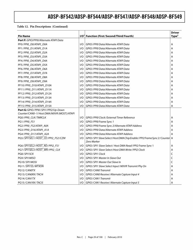
ADSP-BF542/ADSP-BF544/ADSP-BF547/ADSP-BF548/ADSP-BF549
Rev. C | Page 29 of 100 | February 2010
Port F: GPIO/PPI0/Alternate ATAPI DataPF0/PPI0_D0/ATAPI_D0A I/O GPIO/PPI0 Data/Alternate ATAPI Data APF1/PPI0_D1/ATAPI_D1A I/O GPIO/PPI0 Data/Alternate ATAPI Data APF2/PPI0_D2/ATAPI_D2A I/O GPIO/PPI0 Data/Alternate ATAPI Data APF3/PPI0_D3/ATAPI_D3A I/O GPIO/PPI0 Data/Alternate ATAPI Data APF4/PPI0_D4/ATAPI_D4A I/O GPIO/PPI0 Data/Alternate ATAPI Data APF5/PPI0_D5/ATAPI_D5A I/O GPIO/PPI0 Data/Alternate ATAPI Data APF6/PPI0_D6/ATAPI_D6A I/O GPIO/PPI0 Data/Alternate ATAPI Data APF7/PPI0_D7/ATAPI_D7A I/O GPIO/PPI0 Data/Alternate ATAPI Data APF8/PPI0_D8/ATAPI_D8A I/O GPIO/PPI0 Data/Alternate ATAPI Data APF9/PPI0_D9/ATAPI_D9A I/O GPIO/PPI0 Data/Alternate ATAPI Data APF10/PPI0_D10/ATAPI_D10A I/O GPIO/PPI0 Data/Alternate ATAPI Data APF11/PPI0_D11/ATAPI_D11A I/O GPIO/PPI0 Data/Alternate ATAPI Data APF12/PPI0_D12/ATAPI_D12A I/O GPIO/PPI0 Data/Alternate ATAPI Data APF13/PPI0_D13/ATAPI_D13A I/O GPIO/PPI0 Data/Alternate ATAPI Data APF14/PPI0_D14/ATAPI_D14A I/O GPIO/PPI0 Data/Alternate ATAPI Data APF15/PPI0_D15/ATAPI_D15A I/O GPIO/PPI0 Data/Alternate ATAPI Data APort G: GPIO/PPI0/SPI1/PPI2/Up-Down Counter/CAN0–1/Host DMA/MXVR (MOST)/ATAPI PG0/PPI0_CLK/TMRCLK I/O GPIO/PPI0 Clock/External Timer Reference APG1/PPI0_FS1 I/O GPIO/PPI0 Frame Sync 1 APG2/PPI0_FS2/ATAPI_A0A I/O GPIO/PPI0 Frame Sync 2/Alternate ATAPI Address APG3/PPI0_D16/ATAPI_A1A I/O GPIO/PPI0 Data/Alternate ATAPI Address APG4/PPI0_D17/ATAPI_A2A I/O GPIO/PPI0 Data/Alternate ATAPI Address APG5/SPI1SEL1/HOST_CE/PPI2_FS2/CZM I/O GPIO/SPI1 Slave Select/Host DMA Chip Enable/PPI2 Frame Sync 2/Counter
Zero MarkerA
PG6/SPI1SEL2/HOST_RD/PPI2_FS1 I/O GPIO/SPI1 Slave Select/ Host DMA Read/PPI2 Frame Sync 1 APG7/SPI1SEL3/HOST_WR/PPI2_CLK I/O GPIO/SPI1 Slave Select/Host DMA Write/PPI2 Clock APG8/SPI1SCK I/O GPIO/SPI1 Clock CPG9/SPI1MISO I/O GPIO/SPI1 Master In Slave Out CPG10/SPI1MOSI I/O GPIO/SPI1 Master Out Slave In CPG11/SPI1SS / MTXON I/O GPIO/SPI1 Slave Select Input/MXVR Transmit Phy On APG12/CAN0TX I/O GPIO/CAN0 Transmit APG13/CAN0RX/TACI4 I/O GPIO/CAN0 Receive/Alternate Capture Input 4 APG14/CAN1TX I/O GPIO/CAN1 Transmit APG15/CAN1RX/TACI5 I/O GPIO/CAN1 Receive/Alternate Capture Input 5 A
Table 12. Pin Descriptions (Continued)
Pin Name I/O1 Function (First/Second/Third/Fourth)Driver Type2
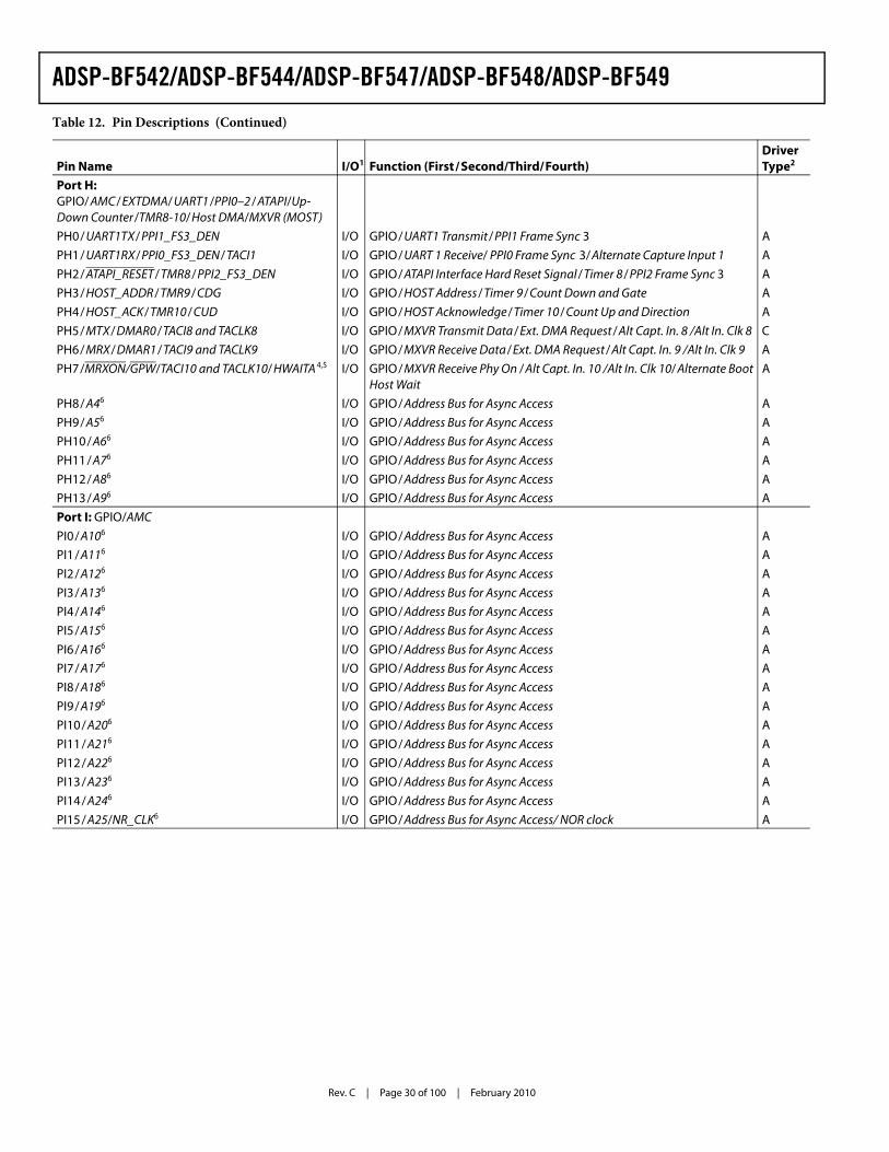
Rev. C | Page 30 of 100 | February 2010
ADSP-BF542/ADSP-BF544/ADSP-BF547/ADSP-BF548/ADSP-BF549
Port H: GPIO/AMC/EXTDMA/UART1/PPI0–2/ATAPI/Up-Down Counter/TMR8-10/Host DMA/MXVR (MOST)PH0/UART1TX/PPI1_FS3_DEN I/O GPIO/UART1 Transmit/PPI1 Frame Sync 3 APH1/UART1RX/PPI0_FS3_DEN/TACI1 I/O GPIO/UART 1 Receive/ PPI0 Frame Sync 3/Alternate Capture Input 1 APH2/ATAPI_RESET/TMR8/PPI2_FS3_DEN I/O GPIO/ATAPI Interface Hard Reset Signal/Timer 8/PPI2 Frame Sync 3 APH3/HOST_ADDR /TMR9/CDG I/O GPIO/HOST Address/Timer 9/Count Down and Gate APH4/HOST_ACK/TMR10/CUD I/O GPIO/HOST Acknowledge/Timer 10/Count Up and Direction APH5/MTX/DMAR0/TACI8 and TACLK8 I/O GPIO/MXVR Transmit Data/Ext. DMA Request/Alt Capt. In. 8 /Alt In. Clk 8 CPH6/MRX/DMAR1/TACI9 and TACLK9 I/O GPIO/MXVR Receive Data/Ext. DMA Request/Alt Capt. In. 9 /Alt In. Clk 9 APH7/MRXON/GPW/TACI10 and TACLK10/HWAITA 4,5 I/O GPIO/MXVR Receive Phy On /Alt Capt. In. 10 /Alt In. Clk 10/Alternate Boot
Host WaitA
PH8/A46 I/O GPIO/Address Bus for Async Access APH9/A56 I/O GPIO/Address Bus for Async Access APH10/A66 I/O GPIO/Address Bus for Async Access APH11/A76 I/O GPIO/Address Bus for Async Access APH12/A86 I/O GPIO/Address Bus for Async Access APH13/A96 I/O GPIO/Address Bus for Async Access APort I: GPIO/AMCPI0/A106 I/O GPIO/Address Bus for Async Access API1/A116 I/O GPIO/Address Bus for Async Access API2/A126 I/O GPIO/Address Bus for Async Access API3/A136 I/O GPIO/Address Bus for Async Access API4/A146 I/O GPIO/Address Bus for Async Access API5/A156 I/O GPIO/Address Bus for Async Access API6/A166 I/O GPIO/Address Bus for Async Access API7/A176 I/O GPIO/Address Bus for Async Access API8/A186 I/O GPIO/Address Bus for Async Access API9/A196 I/O GPIO/Address Bus for Async Access API10/A206 I/O GPIO/Address Bus for Async Access API11/A216 I/O GPIO/Address Bus for Async Access API12/A226 I/O GPIO/Address Bus for Async Access API13/A236 I/O GPIO/Address Bus for Async Access API14/A246 I/O GPIO/Address Bus for Async Access API15/A25/NR_CLK6 I/O GPIO/Address Bus for Async Access/ NOR clock A
Table 12. Pin Descriptions (Continued)
Pin Name I/O1 Function (First/Second/Third/Fourth)Driver Type2
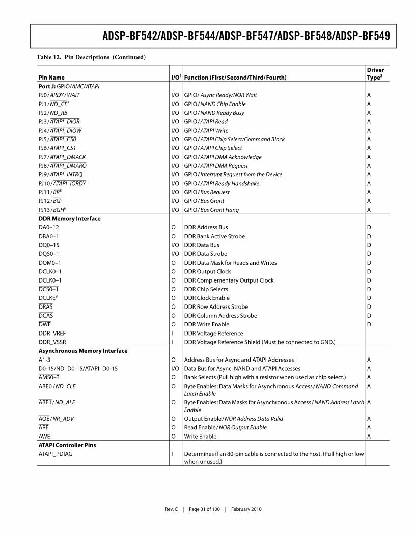
ADSP-BF542/ADSP-BF544/ADSP-BF547/ADSP-BF548/ADSP-BF549
Rev. C | Page 31 of 100 | February 2010
Port J: GPIO/AMC/ATAPI PJ0/ARDY/WAIT I/O GPIO/ Async Ready/NOR Wait APJ1/ND_CE7 I/O GPIO/NAND Chip Enable APJ2/ND_RB I/O GPIO/NAND Ready Busy APJ3/ATAPI_DIOR I/O GPIO/ATAPI Read APJ4/ATAPI_DIOW I/O GPIO/ATAPI Write APJ5/ATAPI_CS0 I/O GPIO/ATAPI Chip Select/Command Block APJ6/ATAPI_CS1 I/O GPIO/ATAPI Chip Select APJ7/ATAPI_DMACK I/O GPIO/ATAPI DMA Acknowledge APJ8/ATAPI_DMARQ I/O GPIO/ATAPI DMA Request APJ9/ATAPI_INTRQ I/O GPIO/ Interrupt Request from the Device APJ10/ATAPI_IORDY I/O GPIO/ATAPI Ready Handshake APJ11/BR8 I/O GPIO/Bus Request APJ12/BG6 I/O GPIO/Bus Grant APJ13/BGH6 I/O GPIO/Bus Grant Hang ADDR Memory InterfaceDA0–12 O DDR Address Bus DDBA0–1 O DDR Bank Active Strobe DDQ0–15 I/O DDR Data Bus DDQS0–1 I/O DDR Data Strobe DDQM0–1 O DDR Data Mask for Reads and Writes DDCLK0–1 O DDR Output Clock DDCLK0–1 O DDR Complementary Output Clock DDCS0–1 O DDR Chip Selects DDCLKE9 O DDR Clock Enable DDRAS O DDR Row Address Strobe DDCAS O DDR Column Address Strobe DDWE O DDR Write Enable DDDR_VREF I DDR Voltage ReferenceDDR_VSSR I DDR Voltage Reference Shield (Must be connected to GND.)Asynchronous Memory InterfaceA1-3 O Address Bus for Async and ATAPI Addresses AD0-15/ND_D0-15/ATAPI_D0-15 I/O Data Bus for Async, NAND and ATAPI Accesses AAMS0–3 O Bank Selects (Pull high with a resistor when used as chip select.) AABE0 /ND_CLE O Byte Enables :Data Masks for Asynchronous Access/NAND Command
Latch EnableA
ABE1/ND_ALE O Byte Enables:Data Masks for Asynchronous Access/NAND Address Latch Enable
A
AOE/NR_ADV O Output Enable/NOR Address Data Valid AARE O Read Enable/NOR Output Enable AAWE O Write Enable AATAPI Controller PinsATAPI_PDIAG I Determines if an 80-pin cable is connected to the host. (Pull high or low
when unused.)
Table 12. Pin Descriptions (Continued)
Pin Name I/O1 Function (First/Second/Third/Fourth)Driver Type2
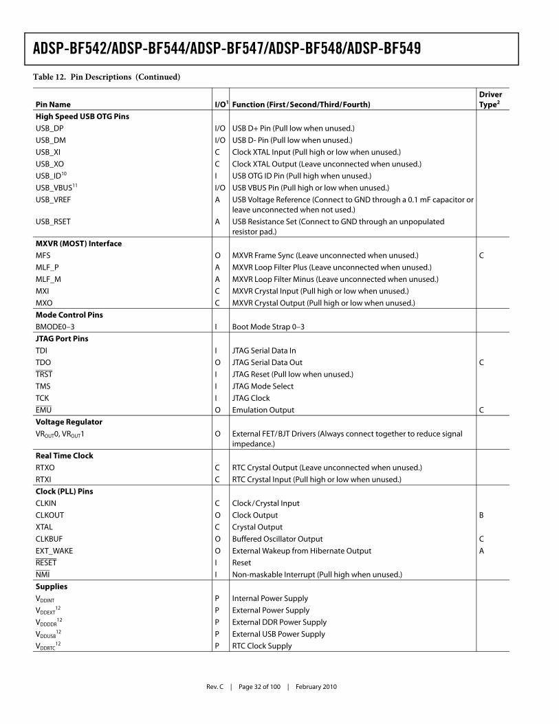
Rev. C | Page 32 of 100 | February 2010
ADSP-BF542/ADSP-BF544/ADSP-BF547/ADSP-BF548/ADSP-BF549
High Speed USB OTG PinsUSB_DP I/O USB D+ Pin (Pull low when unused.)USB_DM I/O USB D- Pin (Pull low when unused.)USB_XI C Clock XTAL Input (Pull high or low when unused.)USB_XO C Clock XTAL Output (Leave unconnected when unused.)USB_ID10 I USB OTG ID Pin (Pull high when unused.)USB_VBUS11 I/O USB VBUS Pin (Pull high or low when unused.)USB_VREF A USB Voltage Reference (Connect to GND through a 0.1 mF capacitor or
leave unconnected when not used.)USB_RSET A USB Resistance Set (Connect to GND through an unpopulated
resistor pad.)MXVR (MOST) InterfaceMFS O MXVR Frame Sync (Leave unconnected when unused.) CMLF_P A MXVR Loop Filter Plus (Leave unconnected when unused.)MLF_M A MXVR Loop Filter Minus (Leave unconnected when unused.)MXI C MXVR Crystal Input (Pull high or low when unused.)MXO C MXVR Crystal Output (Pull high or low when unused.)Mode Control PinsBMODE0–3 I Boot Mode Strap 0–3JTAG Port PinsTDI I JTAG Serial Data InTDO O JTAG Serial Data Out CTRST I JTAG Reset (Pull low when unused.)TMS I JTAG Mode SelectTCK I JTAG ClockEMU O Emulation Output CVoltage RegulatorVROUT0, VROUT1 O External FET/BJT Drivers (Always connect together to reduce signal
impedance.)Real Time ClockRTXO C RTC Crystal Output (Leave unconnected when unused.)RTXI C RTC Crystal Input (Pull high or low when unused.)Clock (PLL) PinsCLKIN C Clock/Crystal InputCLKOUT O Clock Output BXTAL C Crystal OutputCLKBUF O Buffered Oscillator Output CEXT_WAKE O External Wakeup from Hibernate Output ARESET I ResetNMI I Non-maskable Interrupt (Pull high when unused.)SuppliesVDDINT P Internal Power SupplyVDDEXT
12 P External Power SupplyVDDDDR
12 P External DDR Power SupplyVDDUSB
12 P External USB Power SupplyVDDRTC
12 P RTC Clock Supply
Table 12. Pin Descriptions (Continued)
Pin Name I/O1 Function (First/Second/Third/Fourth)Driver Type2
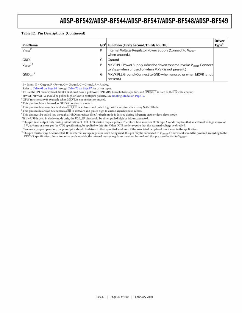
ADSP-BF542/ADSP-BF544/ADSP-BF547/ADSP-BF548/ADSP-BF549
Rev. C | Page 33 of 100 | February 2010
VDDVR13 P Internal Voltage Regulator Power Supply (Connect to VDDEXT
when unused.)GND G GroundVDDMP
12 P MXVR PLL Power Supply. (Must be driven to same level as VDDINT. Connect to VDDINT when unused or when MXVR is not present.)
GNDMP12 G MXVR PLL Ground (Connect to GND when unused or when MXVR is not
present.)1 I = Input, O = Output, P =Power, G = Ground, C = Crystal, A = Analog.2 Refer to Table 61 on Page 86 through Table 70 on Page 87 for driver types.3 To use the SPI memory boot, SPI0SCK should have a pulldown, SPI0MISO should have a pullup, and SPI0SEL1 is used as the CS with a pullup.4 HWAIT/HWAITA should be pulled high or low to configure polarity. See Booting Modes on Page 19.5 GPW functionality is available when MXVR is not present or unused.6 This pin should not be used as GPIO if booting in mode 1.7 This pin should always be enabled as ND_CE in software and pulled high with a resistor when using NAND flash.8 This pin should always be enabled as BR in software and pulled high to enable asynchronous access.9 This pin must be pulled low through a 10kOhm resistor if self-refresh mode is desired during hibernate state or deep-sleep mode.10If the USB is used in device mode only, the USB_ID pin should be either pulled high or left unconnected.11This pin is an output only during initialization of USB OTG session request pulses. Therefore, host mode or OTG type A mode requires that an external voltage source of
5 V, at 8 mA or more per the OTG specification, be applied to this pin. Other OTG modes require that this external voltage be disabled.12To ensure proper operation, the power pins should be driven to their specified level even if the associated peripheral is not used in the application.13This pin must always be connected. If the internal voltage regulator is not being used, this pin may be connected to VDDEXT. Otherwise it should be powered according to the
VDDVR specification. For automotive grade models, the internal voltage regulator must not be used and this pin must be tied to VDDEXT.
Table 12. Pin Descriptions (Continued)
Pin Name I/O1 Function (First/Second/Third/Fourth)Driver Type2
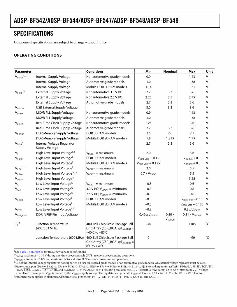
Rev. C | Page 34 of 100 | February 2010
ADSP-BF542/ADSP-BF544/ADSP-BF547/ADSP-BF548/ADSP-BF549
SPECIFICATIONSComponent specifications are subject to change without notice.
OPERATING CONDITIONS
Parameter Conditions Min Nominal Max UnitVDDINT
1, 2 Internal Supply Voltage Nonautomotive grade models 0.9 1.43 VInternal Supply Voltage Automotive grade models 1.0 1.38 VInternal Supply Voltage Mobile DDR SDRAM models 1.14 1.31 V
VDDEXT3 External Supply Voltage Nonautomotive 3.3 V I/O 2.7 3.3 3.6 V
External Supply Voltage Nonautomotive 2.5 V I/O 2.25 2.5 2.75 VExternal Supply Voltage Automotive grade models 2.7 3.3 3.6 V
VDDUSB USB External Supply Voltage 3.0 3.3 3.6 VVDDMP MXVR PLL Supply Voltage Nonautomotive grade models 0.9 1.43 V
MXVR PLL Supply Voltage Automotive grade models 1.0 1.38 VVDDRTC Real Time Clock Supply Voltage Nonautomotive grade models 2.25 3.6 V
Real Time Clock Supply Voltage Automotive grade models 2.7 3.3 3.6 VVDDDDR DDR Memory Supply Voltage DDR SDRAM models 2.5 2.6 2.7 V
DDR Memory Supply Voltage Mobile DDR SDRAM models 1.8 1.875 1.95 VVDDVR
4 Internal Voltage Regulator Supply Voltage
2.7 3.3 3.6 V
VIH High Level Input Voltage5, 6 VDDEXT = maximum 2.0 3.6 VVIHDDR High Level Input Voltage7 DDR SDRAM models VDDR_VREF + 0.15 VDDDDR + 0.3 V
High Level Input Voltage7 Mobile DDR SDRAM models VDDR_VREF + 0.125 VDDDDR + 0.3 VVIH5V
12 High Level Input Voltage8 VDDEXT = maximum 2.0 5.5 VVIHTWI High Level Input Voltage 9, 13 VDDEXT = maximum 0.7 x VDDEXT 5.5 VVIHUSB High Level Input Voltage10 5.25 VVIL Low Level Input Voltage5, 11 VDDEXT = minimum –0.3 0.6 VVIL5V Low Level Input Voltage12 3.3 V I/O, VDDEXT = minimum –0.3 0.8 V
Low Level Input Voltage12 2.5 V I/O, VDDEXT = minimum –0.3 0.6 VVILDDR Low Level Input Voltage7 DDR SDRAM models –0.3 VDDR_VREF – 0.15 V
Low Level Input Voltage7 Mobile DDR SDRAM models –0.3 VDDR_VREF – 0.125 VVILTWI Low Level Input Voltage9, 13 –0.3 0.3 x VDDEXT VVDDR_VREF DDR_VREF Pin Input Voltage 0.49 x VDDDDR 0.50 x
VDDDDR
0.51 x VDDDDR V
TJ14 Junction Temperature
(400/533 MHz)400-Ball Chip Scale Package Ball Grid Array (CSP_BGA) @TAMBIENT = –40ºC to +85ºC
–40 +105 ºC
Junction Temperature (600 MHz) 400-Ball Chip Scale Package Ball Grid Array (CSP_BGA) @TAMBIENT = 0ºC to +70ºC
0 +90 ºC
1 See Table 13 on Page 35 for frequency/voltage specifications.2 VDDINT maximum is 1.10 V during one-time-programmable (OTP) memory programming operations.3 VDDEXT minimum is 3.0 V and maximum is 3.6 V during OTP memory programming operations.4 Use of the internal voltage regulator is not supported on 600 MHz speed grade models or on automotive grade models. An external voltage regulator must be used.5 Bidirectional pins (D15–0, PA15–0, PB14–0, PC15–0, PD15–0, PE15–0, PF15–0, PG15–0, PH13–0, PI15–0, PJ14–0) and input pins (ATAPI_PDIAG, USB_ID, TCK, TDI,
TMS, TRST, CLKIN, RESET, NMI, and BMODE3–0) of the ADSP-BF54x Blackfin processors are 3.3 V-tolerant (always accept up to 3.6 V maximum VIH). Voltage compliance (on outputs, VOH) is limited by the VDDEXT supply voltage. The regulator can generate VDDINT at levels of 0.90 V to 1.30 V with -5% to +5% tolerance.
6 Parameter value applies to all input and bidirectional pins except PB1-0, PE15-14, PG15–11, PH7-6, DQ0-15, and DQS0-1.
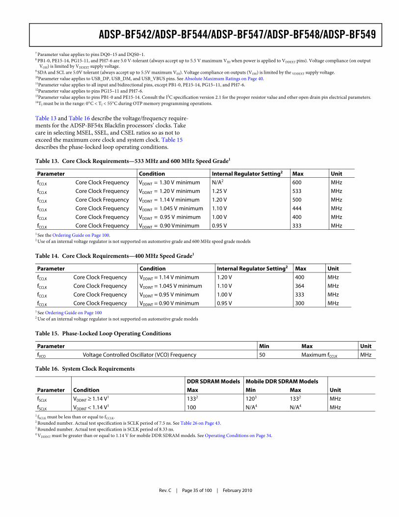
ADSP-BF542/ADSP-BF544/ADSP-BF547/ADSP-BF548/ADSP-BF549
Rev. C | Page 35 of 100 | February 2010
Table 13 and Table 16 describe the voltage/frequency require-ments for the ADSP-BF54x Blackfin processors’ clocks. Take care in selecting MSEL, SSEL, and CSEL ratios so as not to exceed the maximum core clock and system clock. Table 15 describes the phase-locked loop operating conditions.
7 Parameter value applies to pins DQ0–15 and DQS0–1.8 PB1-0, PE15-14, PG15-11, and PH7-6 are 5.0 V-tolerant (always accept up to 5.5 V maximum VIH when power is applied to VDDEXT pins). Voltage compliance (on output
VOH) is limited by VDDEXT supply voltage.9 SDA and SCL are 5.0V tolerant (always accept up to 5.5V maximum VIH). Voltage compliance on outputs (VOH) is limited by the VDDEXT supply voltage.10Parameter value applies to USB_DP, USB_DM, and USB_VBUS pins. See Absolute Maximum Ratings on Page 40.11Parameter value applies to all input and bidirectional pins, except PB1-0, PE15-14, PG15–11, and PH7-6.12Parameter value applies to pins PG15–11 and PH7-6.13Parameter value applies to pins PB1-0 and PE15-14. Consult the I2C specification version 2.1 for the proper resistor value and other open drain pin electrical parameters.14TJ must be in the range: 0°C < TJ < 55°C during OTP memory programming operations.
Table 13. Core Clock Requirements—533 MHz and 600 MHz Speed Grade1
Parameter Condition Internal Regulator Setting2 Max UnitfCCLK Core Clock Frequency VDDINT = 1.30 V minimum N/A2 600 MHzfCCLK Core Clock Frequency VDDINT = 1.20 V minimum 1.25 V 533 MHzfCCLK Core Clock Frequency VDDINT = 1.14 V minimum 1.20 V 500 MHzfCCLK Core Clock Frequency VDDINT = 1.045 V minimum 1.10 V 444 MHzfCCLK Core Clock Frequency VDDINT = 0.95 V minimum 1.00 V 400 MHzfCCLK Core Clock Frequency VDDINT = 0.90 Vminimum 0.95 V 333 MHz
1 See the Ordering Guide on Page 100. 2 Use of an internal voltage regulator is not supported on automotive grade and 600 MHz speed grade models
Table 14. Core Clock Requirements—400 MHz Speed Grade1
Parameter Condition Internal Regulator Setting2 Max UnitfCCLK Core Clock Frequency VDDINT = 1.14 V minimum 1.20 V 400 MHzfCCLK Core Clock Frequency VDDINT = 1.045 V minimum 1.10 V 364 MHzfCCLK Core Clock Frequency VDDINT = 0.95 V minimum 1.00 V 333 MHzfCCLK Core Clock Frequency VDDINT = 0.90 V minimum 0.95 V 300 MHz
1 See Ordering Guide on Page 1002 Use of an internal voltage regulator is not supported on automotive grade models
Table 15. Phase-Locked Loop Operating Conditions
Parameter Min Max UnitfVCO Voltage Controlled Oscillator (VCO) Frequency 50 Maximum fCCLK MHz
Table 16. System Clock Requirements
Parameter ConditionDDR SDRAM Models Mobile DDR SDRAM Models
UnitMax Min MaxfSCLK VDDINT ≥ 1.14 V1 1332 1203 1332 MHzfSCLK VDDINT < 1.14 V1 100 N/A4 N/A4 MHz
1 fSCLK must be less than or equal to fCCLK.2 Rounded number. Actual test specification is SCLK period of 7.5 ns. See Table 26 on Page 43.3 Rounded number. Actual test specification is SCLK period of 8.33 ns.4 VDDINT must be greater than or equal to 1.14 V for mobile DDR SDRAM models. See Operating Conditions on Page 34.
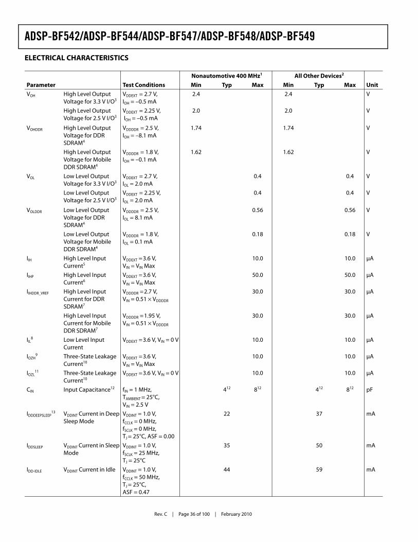
Rev. C | Page 36 of 100 | February 2010
ADSP-BF542/ADSP-BF544/ADSP-BF547/ADSP-BF548/ADSP-BF549
ELECTRICAL CHARACTERISTICS
Nonautomotive 400 MHz1 All Other Devices2
Parameter Test Conditions Min Typ Max Min Typ Max UnitVOH High Level Output
Voltage for 3.3 V I/O3VDDEXT = 2.7 V, IOH = –0.5 mA
2.4 2.4 V
High Level Output Voltage for 2.5 V I/O3
VDDEXT = 2.25 V, IOH = –0.5 mA
2.0 2.0 V
VOHDDR High Level Output Voltage for DDR SDRAM4
VDDDDR = 2.5 V, IOH = –8.1 mA
1.74 1.74 V
High Level Output Voltage for Mobile DDR SDRAM4
VDDDDR = 1.8 V, IOH = –0.1 mA
1.62 1.62 V
VOL Low Level Output Voltage for 3.3 V I/O3
VDDEXT = 2.7 V, IOL = 2.0 mA
0.4 0.4 V
Low Level Output Voltage for 2.5 V I/O3
VDDEXT = 2.25 V, IOL = 2.0 mA
0.4 0.4 V
VOLDDR Low Level Output Voltage for DDR SDRAM4
VDDDDR = 2.5 V, IOL = 8.1 mA
0.56 0.56 V
Low Level Output Voltage for Mobile DDR SDRAM4
VDDDDR = 1.8 V,IOL = 0.1 mA
0.18 0.18 V
IIH High Level Input Current5
VDDEXT =3.6 V, VIN = VIN Max
10.0 10.0 μA
IIHP High Level Input Current6
VDDEXT =3.6 V, VIN = VIN Max
50.0 50.0 μA
IIHDDR_VREF High Level Input Current for DDR SDRAM7
VDDDDR =2.7 V, VIN = 0.51 × VDDDDR
30.0 30.0 μA
High Level Input Current for Mobile DDR SDRAM7
VDDDDR =1.95 V, VIN = 0.51 × VDDDDR
30.0 30.0 μA
IIL8 Low Level Input
CurrentVDDEXT =3.6 V, VIN = 0 V 10.0 10.0 μA
IOZH9 Three-State Leakage
Current10VDDEXT =3.6 V, VIN = VIN Max
10.0 10.0 μA
IOZL11 Three-State Leakage
Current10VDDEXT =3.6 V, VIN = 0 V 10.0 10.0 μA
CIN Input Capacitance12 fIN = 1 MHz, TAMBIENT = 25°C, VIN = 2.5 V
412 812 412 812 pF
IDDDEEPSLEEP13 VDDINT Current in Deep
Sleep ModeVDDINT = 1.0 V,fCCLK = 0 MHz,fSCLK = 0 MHz,TJ = 25°C, ASF = 0.00
22 37 mA
IDDSLEEP VDDINT Current in Sleep Mode
VDDINT = 1.0 V, fSCLK = 25 MHz, TJ = 25°C
35 50 mA
IDD-IDLE VDDINT Current in Idle VDDINT = 1.0 V, fCCLK = 50 MHz, TJ = 25°C, ASF = 0.47
44 59 mA
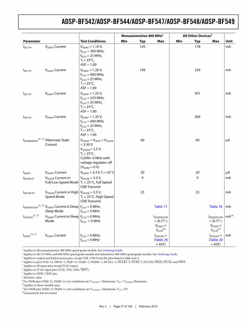
ADSP-BF542/ADSP-BF544/ADSP-BF547/ADSP-BF548/ADSP-BF549
Rev. C | Page 37 of 100 | February 2010
IDD-TYP VDDINT Current VDDINT = 1.10 V, fCCLK = 300 MHz, fSCLK = 25 MHz, TJ = 25°C, ASF = 1.00
145 178 mA
IDD-TYP VDDINT Current VDDINT = 1.20 V, fCCLK = 400 MHz, fSCLK = 25 MHz, TJ = 25°C, ASF = 1.00
199 239 mA
IDD-TYP VDDINT Current VDDINT = 1.25 V,fCCLK = 533 MHz, fSCLK = 25 MHz, TJ = 25°C, ASF = 1.00
301 mA
IDD-TYP VDDINT Current VDDINT = 1.35 V, fCCLK = 600 MHz, fSCLK = 25 MHz, TJ = 25°C, ASF = 1.00
360 mA
IDDHIBERNATE13, 14 Hibernate State
CurrentVDDEXT = VDDVR = VDDUSB
= 3.30 V, VDDDDR = 2.5 V, TJ = 25°C, CLKIN= 0 MHz with voltage regulator off (VDDINT = 0 V)
60 60 µA
IDDRTC VDDRTC Current VDDRTC = 3.3 V, TJ = 25°C 20 20 µAIDDUSB-FS VDDUSB Current in
Full/Low Speed ModeVDDUSB = 3.3 V, TJ = 25°C, Full Speed USB Transmit
9 9 mA
IDDUSB-HS VDDUSB Current in High Speed Mode
VDDUSB = 3.3 V, TJ = 25°C, High Speed USB Transmit
25 25 mA
IDDDEEPSLEEP13, 15 VDDINT Current in Deep
Sleep ModefCCLK = 0 MHz, fSCLK = 0 MHz
Table 17 Table 18 mA
IDDSLEEP13, 15 VDDINIT Current in Sleep
ModefCCLK = 0 MHz, fSCLK > 0 MHz
IDDDEEPSLEEP + (0.77 × VDDINT × fSCLK)16
IDDDEEPSLEEP + (0.77 × VDDINT × fSCLK)16
mA16
IDDINT15, 17 VDDINT Current fCCLK > 0 MHz,
fSCLK > 0 MHzIDDSLEEP + (Table 20
× ASF)
IDDSLEEP + (Table 20
× ASF)
mA
1 Applies to all nonautomotive 400 MHz speed grade models. See Ordering Guide. 2 Applies to all 533 MHz and 600 MHz speed grade models and automotive 400 MHz speed grade models. See Ordering Guide. 3 Applies to output and bidirectional pins, except USB_VBUS and the pins listed in table note 4. 4 Applies to pins DA0–12, DBA0–1, DQ0–15, DQS0–1, DQM0–1, DCLK1–2, DCLK1–2, DCS0–1, DCLKE, DRAS, DCAS, and DWE.5 Applies to all input pins except JTAG inputs.6 Applies to JTAG input pins (TCK, TDI, TMS, TRST).7 Applies to DDR_VREF pin.8 Absolute value.9 For DDR pins (DQ0-15, DQS0-1), test conditions are VDDDDR = Maximum, VIN = VDDDDR Maximum.10Applies to three-statable pins.11For DDR pins (DQ0-15, DQS0-1), test conditions are VDDDDR = Maximum, VIN = 0V.12Guaranteed, but not tested
Nonautomotive 400 MHz1 All Other Devices2
Parameter Test Conditions Min Typ Max Min Typ Max Unit
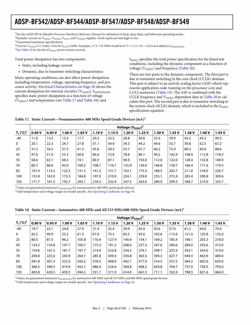
Rev. C | Page 38 of 100 | February 2010
ADSP-BF542/ADSP-BF544/ADSP-BF547/ADSP-BF548/ADSP-BF549
Total power dissipation has two components:• Static, including leakage current• Dynamic, due to transistor switching characteristics
Many operating conditions can also affect power dissipation, including temperature, voltage, operating frequency, and pro-cessor activity. Electrical Characteristics on Page 36 shows the current dissipation for internal circuitry (VDDINT). IDDDEEPSLEEP specifies static power dissipation as a function of voltage (VDDINT) and temperature (see Table 17 and Table 18), and
IDDINT specifies the total power specification for the listed test conditions, including the dynamic component as a function of voltage (VDDINT) and frequency (Table 20). There are two parts to the dynamic component. The first part is due to transistor switching in the core clock (CCLK) domain. This part is subject to an activity scaling factor (ASF) which rep-resents application code running on the processor core and L1/L2 memories (Table 19). The ASF is combined with the CCLK frequency and VDDINT dependent data in Table 20 to cal-culate this part. The second part is due to transistor switching in the system clock (SCLK) domain, which is included in the IDDINT specification equation.
13See the ADSP-BF54x Blackfin Processor Hardware Reference Manual for definition of sleep, deep sleep, and hibernate operating modes.14Includes current on VDDEXT, VDDUSB, VDDVR, and VDDDDR supplies. Clock inputs are tied high or low.15Guaranteed maximum specifications.16Unit for VDDINT is V (volts). Unit for fSCLK is MHz. Example: 1.2 V, 133 MHz would be 0.77 × 1.2 × 133 = 122.9 mA added to IDDDEEPSLEEP.17See Table 19 for the list of IDDINT power vectors covered.
Table 17. Static Current—Nonautomotive 400 MHz Speed Grade Devices (mA)1
Voltage (VDDINT)2
TJ (°C)2 0.90 V 0.95 V 1.00 V 1.05 V 1.10 V 1.15 V 1.20 V 1.25 V 1.30 V 1.35 V 1.38 V 1.40 V 1.43 V-40 11.9 13.5 15.5 17.7 20.3 23.3 26.8 30.6 35.0 39.9 43.2 45.5 49.50 20.1 22.3 24.7 27.8 31.1 34.9 39.3 44.2 49.6 55.7 59.8 62.5 67.225 31.2 34.2 37.5 41.3 45.6 50.3 55.7 61.7 68.2 75.4 80.3 83.6 88.645 47.0 51.0 55.5 60.6 66.0 72.0 78.8 86.1 94.2 102.9 108.9 112.8 118.255 58.6 63.1 68.3 74.1 80.3 87.1 94.9 103.0 112.0 122.0 128.4 132.8 140.070 80.7 86.6 93.0 100.2 108.1 116.7 125.9 136.0 146.8 158.7 166.4 171.6 179.585 107.0 114.3 122.5 131.5 141.2 151.7 163.1 175.3 188.5 202.7 211.8 218.0 226.7100 153.9 163.0 173.3 184.8 197.0 210.0 224.1 239.0 255.1 272.4 283.4 290.8 300.6105 171.7 181.5 192.7 205.1 218.3 232.4 247.5 263.6 280.9 299.3 308.7 314.9 325.7
1 Values are guaranteed maximum IDDDEEPSLEEP for nonautomotive 400 MHz speed-grade devices.2 Valid temperature and voltage ranges are model-specific. See Operating Conditions on Page 34.
Table 18. Static Current—Automotive 400 MHz and All 533 MHz/600 MHz Speed Grade Devices (mA)1
TJ (°C)2Voltage (VDDINT)2
0.90 V 0.95 V 1.00 V 1.05 V 1.10 V 1.15 V 1.20 V 1.25 V 1.30 V 1.35 V 1.38 V 1.40 V 1.43 V-40 19.7 22.1 24.8 27.9 31.4 35.4 39.9 45.0 50.6 57.0 61.2 64.0 70.40 45.2 49.9 55.2 61.3 67.9 75.3 83.5 92.6 102.6 113.6 121.0 125.8 135.025 80.0 87.5 96.2 105.8 116.4 127.9 140.4 154.1 169.2 185.4 196.1 203.3 218.045 124.2 134.8 147.1 160.7 175.3 191.2 208.6 227.3 247.6 269.6 284.0 293.6 312.055 154.6 167.2 181.7 197.7 214.9 233.8 254.2 276.1 299.7 325.9 343.1 354.6 374.070 209.8 225.6 243.9 264.1 285.8 309.4 334.8 363.5 394.3 427.7 449.4 463.9 489.085 281.8 301.3 323.5 350.2 378.5 408.9 442.1 477.9 516.5 557.5 584.2 602.0 629.0100 366.5 390.5 419.4 452.1 486.9 524.4 564.8 608.2 654.8 704.7 737.0 758.5 793.0105 403.8 428.3 459.5 494.3 531.7 571.9 614.9 661.5 711.1 763.9 798.5 821.6 864.0
1 Values are guaranteed maximum IDDDEEPSLEEP for automotive 400 MHz and all 533 MHz and 600 MHz speed grade devices.2 Valid temperature and voltage ranges are model-specific. See Operating Conditions on Page 34.
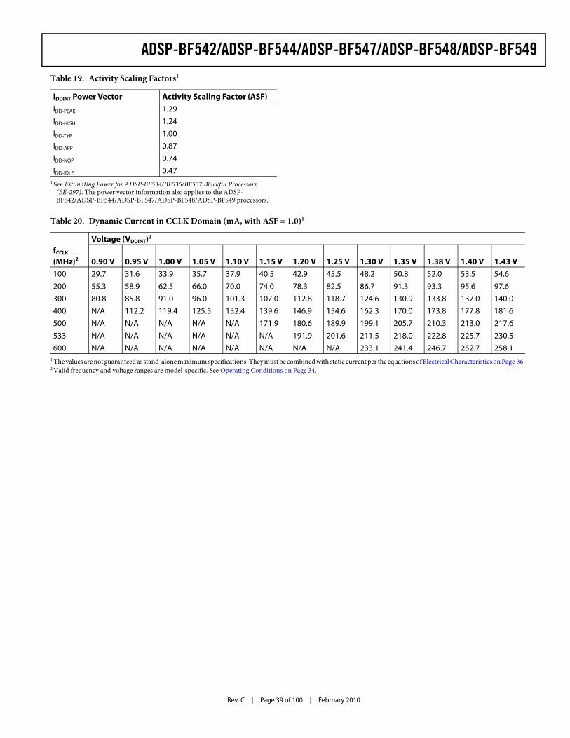
ADSP-BF542/ADSP-BF544/ADSP-BF547/ADSP-BF548/ADSP-BF549
Rev. C | Page 39 of 100 | February 2010
Table 19. Activity Scaling Factors1
IDDINT Power Vector Activity Scaling Factor (ASF)IDD-PEAK 1.29IDD-HIGH 1.24IDD-TYP 1.00IDD-APP 0.87IDD-NOP 0.74IDD-IDLE 0.47
1 See Estimating Power for ADSP-BF534/BF536/BF537 Blackfin Processors (EE-297). The power vector information also applies to the ADSP-BF542/ADSP-BF544/ADSP-BF547/ADSP-BF548/ADSP-BF549 processors.
Table 20. Dynamic Current in CCLK Domain (mA, with ASF = 1.0)1
fCCLK
(MHz)2
Voltage (VDDINT)2
0.90 V 0.95 V 1.00 V 1.05 V 1.10 V 1.15 V 1.20 V 1.25 V 1.30 V 1.35 V 1.38 V 1.40 V 1.43 V100 29.7 31.6 33.9 35.7 37.9 40.5 42.9 45.5 48.2 50.8 52.0 53.5 54.6200 55.3 58.9 62.5 66.0 70.0 74.0 78.3 82.5 86.7 91.3 93.3 95.6 97.6300 80.8 85.8 91.0 96.0 101.3 107.0 112.8 118.7 124.6 130.9 133.8 137.0 140.0400 N/A 112.2 119.4 125.5 132.4 139.6 146.9 154.6 162.3 170.0 173.8 177.8 181.6500 N/A N/A N/A N/A N/A 171.9 180.6 189.9 199.1 205.7 210.3 213.0 217.6533 N/A N/A N/A N/A N/A N/A 191.9 201.6 211.5 218.0 222.8 225.7 230.5600 N/A N/A N/A N/A N/A N/A N/A N/A 233.1 241.4 246.7 252.7 258.1
1 The values are not guaranteed as stand-alone maximum specifications. They must be combined with static current per the equations of Electrical Characteristics on Page 36.2 Valid frequency and voltage ranges are model-specific. See Operating Conditions on Page 34.
Rev. C | Page 40 of 100 | February 2010
ADSP-BF542/ADSP-BF544/ADSP-BF547/ADSP-BF548/ADSP-BF549
ABSOLUTE MAXIMUM RATINGSStresses greater than those listed in Table 21 may cause perma-nent damage to the device. These are stress ratings only. Functional operation of the device at these or any other condi-tions greater than those indicated in the operational sections of this specification is not implied. Exposure to absolute maximum rating conditions for extended periods may affect device reli-ability. Table 22 details the maximum duty cycle for input transient voltage.
The Absolute Maximum Ratings table specifies the maximum total source/sink (IOH/IOL) current for a group of pins. Perma-nent damage can occur if this value is exceeded. To understand this specification, if pins PA4, PA3, PA2, PA1 and PA0 from group 1 in the Total Current Pin Groups table were sourcing or sinking 2 mA each, the total current for those pins would be 10 mA. This would allow up to 70 mA total that could be sourced or sunk by the remaining pins in the group without damaging the device. For a list of all groups and their pins, see
the Total Current Pin Groups table. Note that the VOL and VOH specifications have separate per-pin maximum current require-ments, see the Electrical Characteristics table.
Table 21. Absolute Maximum Ratings
Internal (Core) Supply Voltage (VDDINT) –0.3 V to +1.43 VExternal (I/O) Supply Voltage (VDDEXT) –0.3 V to +3.8 VInput Voltage1, 2, 3
1 Applies to all bidirectional and input only pins except PB1-0, PE15-14, PG15–11, and PH7-6, where the absolute maximum input voltage range is –0.5 V to +5.5 V.
2 Pins USB_DP, USB_DM, and USB_VBUS are 5 V-tolerant when VDDUSB is powered according to the operating conditions table. If VDDUSB supply voltage does not meet the specification in the operating conditions table, these pins could suffer long-term damage when driven to +5 V. If this condition is seen in the application, it can be corrected with additional circuitry to use the external host to power only the VDDUSB pins. Contact factory for application detail and reliability information.
3 Applies only when VDDEXT is within specifications. When VDDEXT is outside speci-fications, the range is VDDEXT ± 0.2 V.
–0.5 V to +3.6 VOutput Voltage Swing –0.5 V to VDDEXT +0.5 VIOH/IOL Current per Single Pin4
4 For more information, see description preceding Table 23.
40 mA (max)IOH/IOL Current per Pin Group4 80 mA (max)Storage Temperature Range –65ºC to +150ºCJunction Temperature Underbias +125ºC
Table 22. Maximum Duty Cycle for Input1 Transient Voltage
1 Does not apply to CLKIN. Absolute maximum for pins PB1-0, PE15-14, PG15-11, and PH7-6 is +5.5V.
VIN Max (V)2
2 Only one of the listed options can apply to a particular design.
VIN Min (V) Maximum Duty Cycle3.63 –0.33 100%3.80 –0.50 48%3.90 –0.60 30%4.00 –0.70 20%4.10 –0.80 10%4.20 –0.90 8%4.30 –1.00 5%
Table 23. Total Current Pin Groups
Group Pins in Group1 PA0, PA1, PA2, PA3, PA4, PA5, PA6, PA7, PA8, PA9, PA10,
PA112 PA12, PA13, PA14, PA15, PB8, PB9, PB10, PB11, PB12,
PB13, PB143 PB0, PB1, PB2, PB3, PB4, PB5, PB6, PB7, BMODE0,
BMODE1, BMODE2, BMODE34 TCK, TDI, TDO, TMS, TRST, PD14, EMU5 PD8, PD9, PD10, PD11, PD12, PD13, PD156 PD0, PD1, PD2, PD3, PD4, PD5, PD6, PD7 7 PE11, PE12, PE13, PF12, PF13, PF14, PF15, PG3, PG4 8 PF4, PF5, PF6, PF7, PF8, PF9, PF10, PF119 PF0, PF1, PF2, PF3, PG0, PG1, PG210 PC0, PC1, PC2, PC3, PC4, PC5, PC6, PC711 PH5, PH6, PH712 A1, A2, A313 PH8, PH9, PH10, PH11, PH12, PH1314 PI0, PI1, PI2, PI3, PI4, PI5, PI6, PI715 PI8, PI9, PI10, PI11, PI12, PI13, PI14, PI1516 AMS0, AMS1, AMS2, AMS3, AOE, CLKBUF, NMI17 CLKIN, XTAL, RESET, RTXI, RTXO, ARE, AWE18 D0, D1, D2, D3, D4, D5, D6, D719 D8, D9, D10, D11, D1220 D13, D14, D15, ABE0, ABE121 EXT_WAKE, CLKOUT, PJ11, PJ12, PJ1322 PJ0, PJ1, PJ2, PJ3, PJ4, PJ5, PJ6, PJ7, ATAPI_PDIAG23 PJ8, PJ9, PJ10, PE7, PG12, PG1324 PE0, PE1, PE2, PE4, PE5, PE6, PE8, PE9, PE10, PH3, PH425 PH0, PH2, PE14, PE15, PG5, PG6, PG7, PG8, PG9, PG10,
PG1126 PC8, PC9, PC10, PC11, PC12, PC13, PE3, PG14, PG15, PH1
ADSP-BF542/ADSP-BF544/ADSP-BF547/ADSP-BF548/ADSP-BF549
Rev. C | Page 41 of 100 | February 2010
ESD SENSITIVITY
PACKAGE INFORMATIONThe information presented in Figure 9 and Table 24 provides information related to specific product features. For a complete listing of product offerings, see the Ordering Guide on Page 100.
ESD (electrostatic discharge) sensitive device.Charged devices and circuit boards can dischargewithout detection. Although this product featurespatented or proprietary protection circuitry, damagemay occur on devices subjected to high energy ESD.Therefore, proper ESD precautions should be taken toavoid performance degradation or loss of functionality.
Figure 9. Product Information on Package
Table 24. Package Information
Brand Key DescriptionBF54x x = 2, 4, 7, 8 or 9(M) Mobile DDR Indicator (optional)t Temperature Rangepp Package TypeZ RoHS Compliant partcc See Ordering Guidevvvvvv.x-q Assembly Lot Coden.n Silicon Revision# RoHS Compliant Designationyyww Date Code
vvvvvv.x-q n.n
tppZ-cc
B
ADSP-BF54x(M)
a
# yywwcountry_of_origin
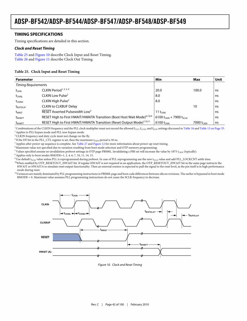
Rev. C | Page 42 of 100 | February 2010
ADSP-BF542/ADSP-BF544/ADSP-BF547/ADSP-BF548/ADSP-BF549
TIMING SPECIFICATIONSTiming specifications are detailed in this section.
Clock and Reset Timing
Table 25 and Figure 10 describe Clock Input and Reset Timing. Table 26 and Figure 11 describe Clock Out Timing.
Table 25. Clock Input and Reset Timing
Parameter Min Max UnitTiming RequirementstCKIN CLKIN Period1, 2, 3, 4 20.0 100.0 nstCKINL CLKIN Low Pulse2 8.0 nstCKINH CLKIN High Pulse2 8.0 nstBUFDLAY CLKIN to CLKBUF Delay 10 nstWRST RESET Asserted Pulsewidth Low5 11 tCKIN nstRHWFT RESET High to First HWAIT/HWAITA Transition (Boot Host Wait Mode)6,7,8,9 6100 tCKIN + 7900 tSCLK nstRHWFT RESET High to First HWAIT/HWAITA Transition (Reset Output Mode)7,10,11 6100 tCKIN 7000 tCKIN ns
1 Combinations of the CLKIN frequency and the PLL clock multiplier must not exceed the allowed fVCO, fCCLK, and fSCLK settings discussed in Table 16 and Table 13 on Page 35.2 Applies to PLL bypass mode and PLL non-bypass mode.3 CLKIN frequency and duty cycle must not change on the fly.4 If the DF bit in the PLL_CTL register is set, then the maximum tCKIN period is 50 ns.5 Applies after power-up sequence is complete. See Table 27 and Figure 12 for more information about power-up reset timing.6 Maximum value not specified due to variation resulting from boot mode selection and OTP memory programming.7 Values specified assume no invalidation preboot settings in OTP page PBS00L. Invalidating a PBS set will increase the value by 1875 tCKIN (typically).8 Applies only to boot modes BMODE=1, 2, 4, 6, 7, 10, 11, 14, 15. 9 Use default tSCLK value unless PLL is reprogrammed during preboot. In case of PLL reprogramming use the new tSCLK value and add PLL_LOCKCNT settle time. 10When enabled by OTP_RESETOUT_HWAIT bit. If regular HWAIT is not required in an application, the OTP_RESETOUT_HWAIT bit in the same page instructs the
HWAIT or HWAITA to simulate reset output functionality. Then an external resistor is expected to pull the signal to the reset level, as the pin itself is in high performance mode during reset.
11Variances are mainly dominated by PLL programming instructions in PBS00L page and boot code differences between silicon revisions. The earlier is bypassed in boot mode BMODE = 0. Maximum value assumes PLL programming instructions do not cause the SCLK frequency to decrease.
Figure 10. Clock and Reset Timing
CLKIN
tWRST
tCKIN
tCKINL tCKINHtBUFDLAY
tBUFDLAY
RESET
CLKBUF
HWAIT (A)
tRHWFT
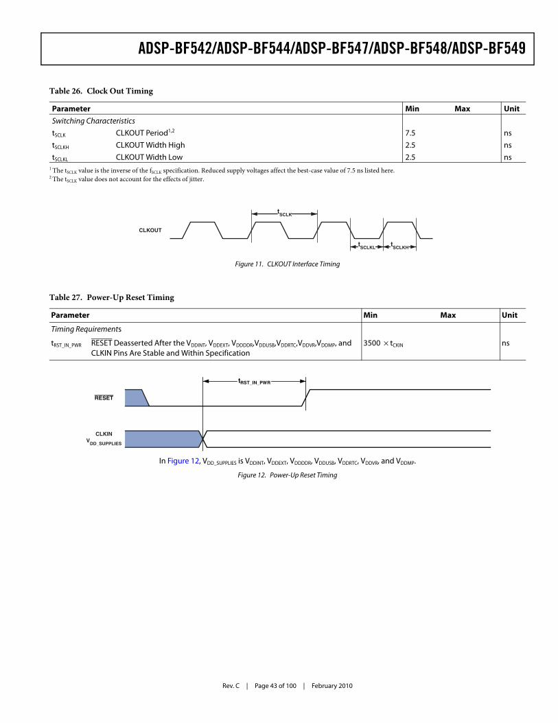
ADSP-BF542/ADSP-BF544/ADSP-BF547/ADSP-BF548/ADSP-BF549
Rev. C | Page 43 of 100 | February 2010
Table 26. Clock Out Timing
Parameter Min Max UnitSwitching CharacteristicstSCLK CLKOUT Period1,2 7.5 nstSCLKH CLKOUT Width High 2.5 nstSCLKL CLKOUT Width Low 2.5 ns
1 The tSCLK value is the inverse of the fSCLK specification. Reduced supply voltages affect the best-case value of 7.5 ns listed here.2 The tSCLK value does not account for the effects of jitter.
Figure 11. CLKOUT Interface Timing
tSCLKL
tSCLKH
tSCLK
CLKOUT
Table 27. Power-Up Reset Timing
Parameter Min Max Unit
Timing Requirements
tRST_IN_PWR RESET Deasserted After the VDDINT, VDDEXT, VDDDDR,VDDUSB,VDDRTC,VDDVR,VDDMP, and CLKIN Pins Are Stable and Within Specification
3500 × tCKIN ns
In Figure 12, VDD_SUPPLIES is VDDINT, VDDEXT, VDDDDR, VDDUSB, VDDRTC, VDDVR, and VDDMP.
Figure 12. Power-Up Reset Timing
RESET
tRST_IN_PWR
CLKINV
DD_SUPPLIES
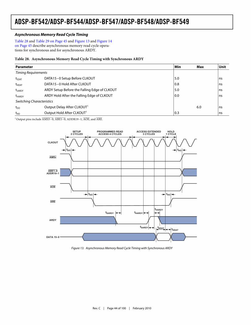
Rev. C | Page 44 of 100 | February 2010
ADSP-BF542/ADSP-BF544/ADSP-BF547/ADSP-BF548/ADSP-BF549
Asynchronous Memory Read Cycle Timing
Table 28 and Table 29 on Page 45 and Figure 13 and Figure 14 on Page 45 describe asynchronous memory read cycle opera-tions for synchronous and for asynchronous ARDY.
Table 28. Asynchronous Memory Read Cycle Timing with Synchronous ARDY
Parameter Min Max Unit
Timing Requirements
tSDAT DATA15–0 Setup Before CLKOUT 5.0 ns
tHDAT DATA15–0 Hold After CLKOUT 0.8 ns
tSARDY ARDY Setup Before the Falling Edge of CLKOUT 5.0 ns
tHARDY ARDY Hold After the Falling Edge of CLKOUT 0.0 ns
Switching Characteristics
tDO Output Delay After CLKOUT1 6.0 ns
tHO Output Hold After CLKOUT1 0.3 ns1 Output pins include AMS3–0, ABE1–0, ADDR19–1, AOE, and ARE.
Figure 13. Asynchronous Memory Read Cycle Timing with Synchronous ARDY
tSARDY tHARDY
tSARDY
tHARDY
SETUP2 CYCLES
PROGRAMMED READACCESS 4 CYCLES
ACCESS EXTENDED3 CYCLES
HOLD1 CYCLE
tDO tHO
tDO
tSDAT tHDAT
CLKOUT
AMSx
ABE1–0ADDR19–1
AOE
ARE
ARDY
DATA 15–0
tHO
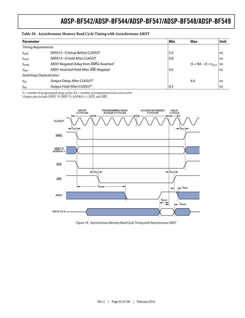
ADSP-BF542/ADSP-BF544/ADSP-BF547/ADSP-BF548/ADSP-BF549
Rev. C | Page 45 of 100 | February 2010
Table 29. Asynchronous Memory Read Cycle Timing with Asynchronous ARDY
Parameter Min Max Unit
Timing Requirements
tSDAT DATA15–0 Setup Before CLKOUT 5.0 ns
tHDAT DATA15–0 Hold After CLKOUT 0.8 ns
tDANR ARDY Negated Delay from AMSx Asserted1 (S + RA – 2) × tSCLK ns
tHAA ARDY Asserted Hold After ARE Negated 0.0 ns
Switching Characteristics
tDO Output Delay After CLKOUT2 6.0 ns
tHO Output Hold After CLKOUT2 0.3 ns1 S = number of programmed setup cycles, RA = number of programmed read access cycles.2 Output pins include AMS3–0, ABE1–0, ADDR19–1, AOE, and ARE.
Figure 14. Asynchronous Memory Read Cycle Timing with Asynchronous ARDY
SETUP2 CYCLES
PROGRAMMED READACCESS 4 CYCLES
ACCESS EXTENDED3 CYCLES
HOLD1 CYCLE
tDO tHO
tDO
tDANR
tSDAT
tHDAT
CLKOUT
AMSx
ABE1–0ADDR19–1
AOE
ARE
ARDY
DATA 15–0
tHO
tHAA
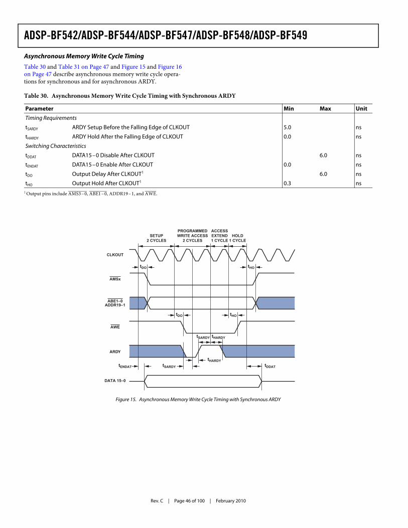
Rev. C | Page 46 of 100 | February 2010
ADSP-BF542/ADSP-BF544/ADSP-BF547/ADSP-BF548/ADSP-BF549
Asynchronous Memory Write Cycle Timing
Table 30 and Table 31 on Page 47 and Figure 15 and Figure 16 on Page 47 describe asynchronous memory write cycle opera-tions for synchronous and for asynchronous ARDY.
Table 30. Asynchronous Memory Write Cycle Timing with Synchronous ARDY
Parameter Min Max Unit
Timing Requirements
tSARDY ARDY Setup Before the Falling Edge of CLKOUT 5.0 ns
tHARDY ARDY Hold After the Falling Edge of CLKOUT 0.0 ns
Switching Characteristics
tDDAT DATA15–0 Disable After CLKOUT 6.0 ns
tENDAT DATA15–0 Enable After CLKOUT 0.0 ns
tDO Output Delay After CLKOUT1 6.0 ns
tHO Output Hold After CLKOUT1 0.3 ns1 Output pins include AMS3–0, ABE1–0, ADDR19–1, and AWE.
Figure 15. Asynchronous Memory Write Cycle Timing with Synchronous ARDY
SETUP2 CYCLES
PROGRAMMEDWRITE ACCESS
2 CYCLES
ACCESSEXTEND1 CYCLE
HOLD1 CYCLE
tDO tHO
CLKOUT
AMSx
ABE1–0ADDR19–1
AWE
DATA 15–0
tDO
tSARDY tDDATtENDAT
tHO
tHARDY
tHARDY
ARDY
tSARDY
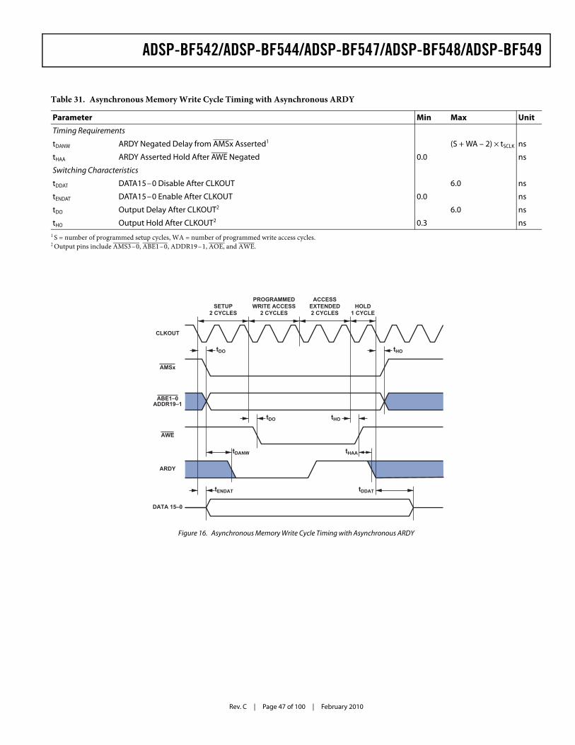
ADSP-BF542/ADSP-BF544/ADSP-BF547/ADSP-BF548/ADSP-BF549
Rev. C | Page 47 of 100 | February 2010
Table 31. Asynchronous Memory Write Cycle Timing with Asynchronous ARDY
Parameter Min Max Unit
Timing Requirements
tDANW ARDY Negated Delay from AMSx Asserted1 (S + WA – 2) × tSCLK ns
tHAA ARDY Asserted Hold After AWE Negated 0.0 ns
Switching Characteristics
tDDAT DATA15–0 Disable After CLKOUT 6.0 ns
tENDAT DATA15–0 Enable After CLKOUT 0.0 ns
tDO Output Delay After CLKOUT2 6.0 ns
tHO Output Hold After CLKOUT2 0.3 ns1 S = number of programmed setup cycles, WA = number of programmed write access cycles.2 Output pins include AMS3–0, ABE1–0, ADDR19–1, AOE, and AWE.
Figure 16. Asynchronous Memory Write Cycle Timing with Asynchronous ARDY
SETUP2 CYCLES
PROGRAMMEDWRITE ACCESS
2 CYCLES
ACCESSEXTENDED2 CYCLES
HOLD1 CYCLE
tDO tHO
CLKOUT
AMSx
ABE1–0ADDR19–1
AWE
ARDY
DATA 15–0
tDO
tDDATtENDAT
tHO
tDANW tHAA
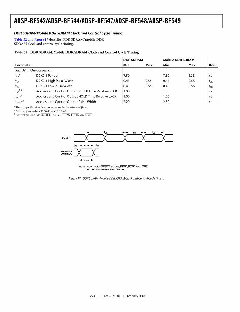
Rev. C | Page 48 of 100 | February 2010
ADSP-BF542/ADSP-BF544/ADSP-BF547/ADSP-BF548/ADSP-BF549
DDR SDRAM/Mobile DDR SDRAM Clock and Control Cycle Timing
Table 32 and Figure 17 describe DDR SDRAM/mobile DDR SDRAM clock and control cycle timing.
Table 32. DDR SDRAM/Mobile DDR SDRAM Clock and Control Cycle Timing
DDR SDRAM Mobile DDR SDRAMUnitParameter Min Max Min Max
Switching CharacteristicstCK
1 DCK0-1 Period 7.50 7.50 8.33 nstCH DCK0-1 High Pulse Width 0.45 0.55 0.45 0.55 tCK
tCL DCK0-1 Low Pulse Width 0.45 0.55 0.45 0.55 tCK
tAS2,3 Address and Control Output SETUP Time Relative to CK 1.00 1.00 ns
tAH2,3 Address and Control Output HOLD Time Relative to CK 1.00 1.00 ns
tOPW2,3 Address and Control Output Pulse Width 2.20 2.30 ns
1 The tCK specification does not account for the effects of jitter. 2 Address pins include DA0-12 and DBA0-1.3 Control pins include DCS0-1, DCLKE, DRAS, DCAS, and DWE.
Figure 17. DDR SDRAM /Mobile DDR SDRAM Clock and Control Cycle Timing
NOTE: CONTROL = DCS0-1, DCLKE, DRAS, DCAS, AND DWE. ADDRESS = DA0-12 AND DBA0-1.
DCK0-1
ADDRESSCONTROL
tAS tAH
tCK tCH tCL
tOPW
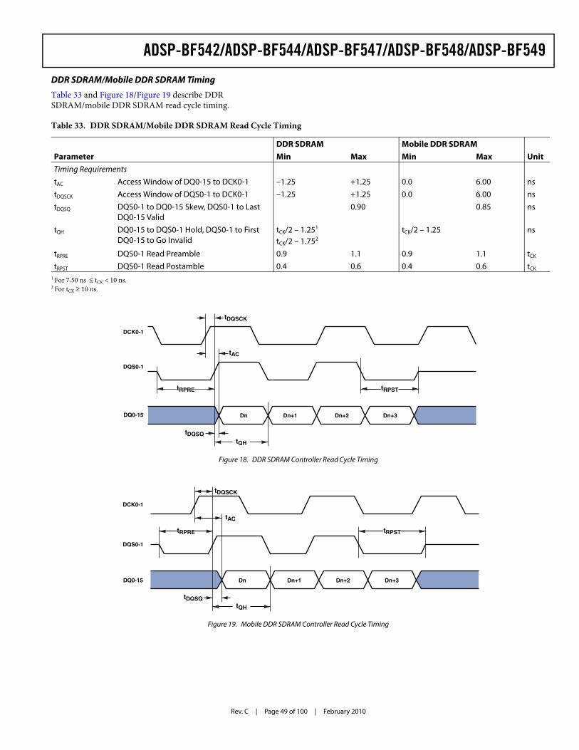
ADSP-BF542/ADSP-BF544/ADSP-BF547/ADSP-BF548/ADSP-BF549
Rev. C | Page 49 of 100 | February 2010
DDR SDRAM/Mobile DDR SDRAM Timing
Table 33 and Figure 18/Figure 19 describe DDR SDRAM/mobile DDR SDRAM read cycle timing.
Table 33. DDR SDRAM/Mobile DDR SDRAM Read Cycle Timing
DDR SDRAM Mobile DDR SDRAMParameter Min Max Min Max UnitTiming RequirementstAC Access Window of DQ0-15 to DCK0-1 –1.25 +1.25 0.0 6.00 nstDQSCK Access Window of DQS0-1 to DCK0-1 –1.25 +1.25 0.0 6.00 nstDQSQ DQS0-1 to DQ0-15 Skew, DQS0-1 to Last
DQ0-15 Valid0.90 0.85 ns
tQH DQ0-15 to DQS0-1 Hold, DQS0-1 to First DQ0-15 to Go Invalid
tCK/2 – 1.251
tCK/2 – 1.752tCK/2 – 1.25 ns
tRPRE DQS0-1 Read Preamble 0.9 1.1 0.9 1.1 tCK
tRPST DQS0-1 Read Postamble 0.4 0.6 0.4 0.6 tCK
1 For 7.50 ns ≤ tCK < 10 ns.2 For tCK ≥ 10 ns.
Figure 18. DDR SDRAM Controller Read Cycle Timing
Figure 19. Mobile DDR SDRAM Controller Read Cycle Timing
DCK0-1
DQS0-1
tDQSCK
tAC
tRPRE
tDQSQtQH
tRPST
DQ0-15 Dn Dn+1 Dn+2 Dn+3
DCK0-1
DQS0-1
tDQSCK
tAC
tDQSQ
DQ0-15 Dn Dn+1 Dn+2 Dn+3
tRPRE tRPST
tQH
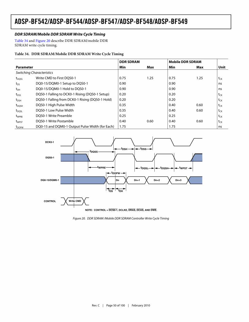
Rev. C | Page 50 of 100 | February 2010
ADSP-BF542/ADSP-BF544/ADSP-BF547/ADSP-BF548/ADSP-BF549
DDR SDRAM/Mobile DDR SDRAM Write Cycle Timing
Table 34 and Figure 20 describe DDR SDRAM/mobile DDR SDRAM write cycle timing.
Table 34. DDR SDRAM/Mobile DDR SDRAM Write Cycle Timing
DDR SDRAM Mobile DDR SDRAMParameter Min Max Min Max UnitSwitching CharacteristicstDQSS Write CMD to First DQS0-1 0.75 1.25 0.75 1.25 tCK
tDS DQ0-15/DQM0-1 Setup to DQS0-1 0.90 0.90 nstDH DQ0-15/DQM0-1 Hold to DQS0-1 0.90 0.90 nstDSS DQS0-1 Falling to DCK0-1 Rising (DQS0-1 Setup) 0.20 0.20 tCK
tDSH DQS0-1 Falling from DCK0-1 Rising (DQS0-1 Hold) 0.20 0.20 tCK
tDQSH DQS0-1 High Pulse Width 0.35 0.40 0.60 tCK
tDQSL DQS0-1 Low Pulse Width 0.35 0.40 0.60 tCK
tWPRE DQS0-1 Write Preamble 0.25 0.25 tCK
tWPST DQS0-1 Write Postamble 0.40 0.60 0.40 0.60 tCK
tDOPW DQ0-15 and DQM0-1 Output Pulse Width (for Each) 1.75 1.75 ns
Figure 20. DDR SDRAM /Mobile DDR SDRAM Controller Write Cycle Timing
DCK0-1
DQS0-1
DQ0-15/DQM0-1
tDQSStDSH tDSS
tDQSL tDQSH tWPSTtWPRE
tDS tDH
tDOPW
CONTROL Write CMD
Dn Dn+1 Dn+2 Dn+3
NOTE: CONTROL = DCS0-1, DCLKE, DRAS, DCAS, AND DWE.
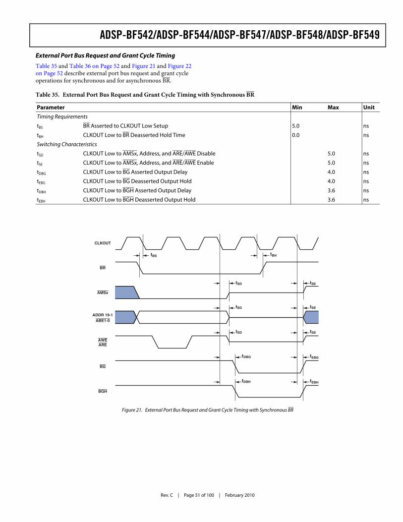
ADSP-BF542/ADSP-BF544/ADSP-BF547/ADSP-BF548/ADSP-BF549
Rev. C | Page 51 of 100 | February 2010
External Port Bus Request and Grant Cycle Timing
Table 35 and Table 36 on Page 52 and Figure 21 and Figure 22 on Page 52 describe external port bus request and grant cycle operations for synchronous and for asynchronous BR.
Table 35. External Port Bus Request and Grant Cycle Timing with Synchronous BR
Parameter Min Max Unit
Timing Requirements
tBS BR Asserted to CLKOUT Low Setup 5.0 ns
tBH CLKOUT Low to BR Deasserted Hold Time 0.0 ns
Switching Characteristics
tSD CLKOUT Low to AMSx, Address, and ARE/AWE Disable 5.0 ns
tSE CLKOUT Low to AMSx, Address, and ARE/AWE Enable 5.0 ns
tDBG CLKOUT Low to BG Asserted Output Delay 4.0 ns
tEBG CLKOUT Low to BG Deasserted Output Hold 4.0 ns
tDBH CLKOUT Low to BGH Asserted Output Delay 3.6 ns
tEBH CLKOUT Low to BGH Deasserted Output Hold 3.6 ns
Figure 21. External Port Bus Request and Grant Cycle Timing with Synchronous BR
AMSx
CLKOUT
BG
BGH
BR
ADDR 19-1ABE1-0
tBHtBS
tSD tSE
tSD
tSD
tSE
tSE
tEBGtDBG
tEBHtDBH
AWEARE
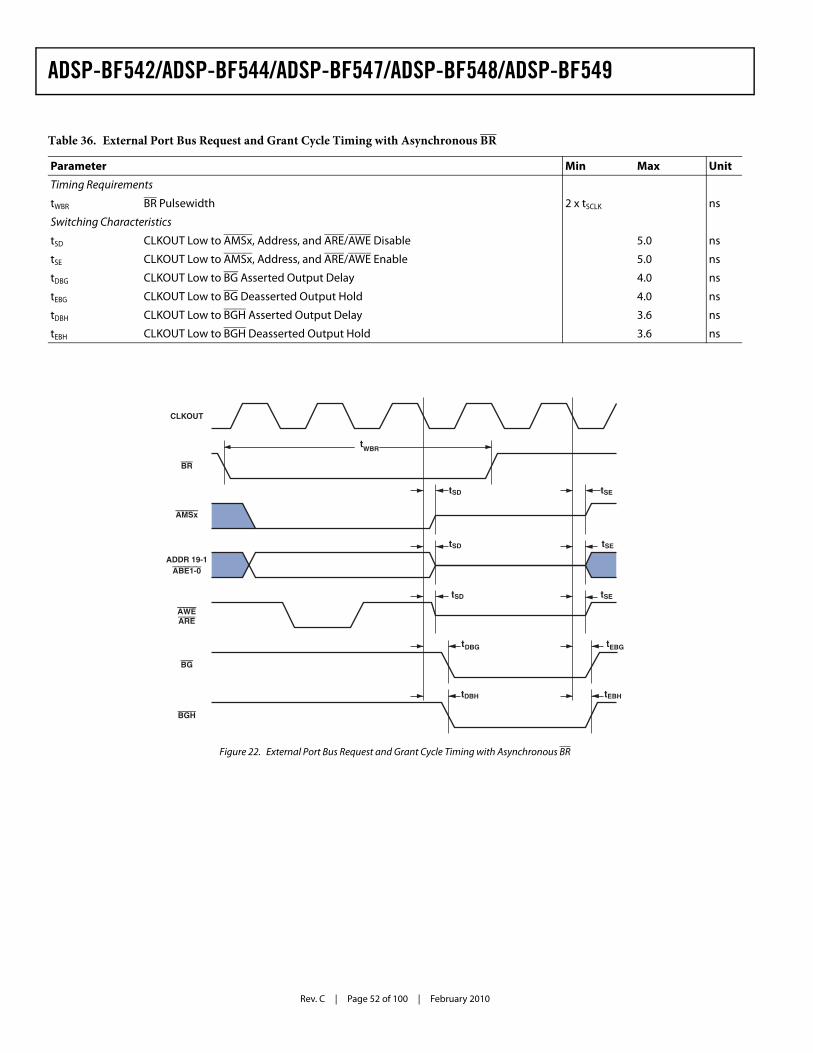
Rev. C | Page 52 of 100 | February 2010
ADSP-BF542/ADSP-BF544/ADSP-BF547/ADSP-BF548/ADSP-BF549
Table 36. External Port Bus Request and Grant Cycle Timing with Asynchronous BR
Parameter Min Max Unit
Timing Requirements
tWBR BR Pulsewidth 2 x tSCLK ns
Switching Characteristics
tSD CLKOUT Low to AMSx, Address, and ARE/AWE Disable 5.0 ns
tSE CLKOUT Low to AMSx, Address, and ARE/AWE Enable 5.0 ns
tDBG CLKOUT Low to BG Asserted Output Delay 4.0 ns
tEBG CLKOUT Low to BG Deasserted Output Hold 4.0 ns
tDBH CLKOUT Low to BGH Asserted Output Delay 3.6 ns
tEBH CLKOUT Low to BGH Deasserted Output Hold 3.6 ns
Figure 22. External Port Bus Request and Grant Cycle Timing with Asynchronous BR
AMSx
CLKOUT
BG
BGH
BR
ADDR 19-1ABE1-0
tSD tSE
tSD
tSD
tSE
tSE
tEBGtDBG
tEBHtDBH
AWEARE
tWBR
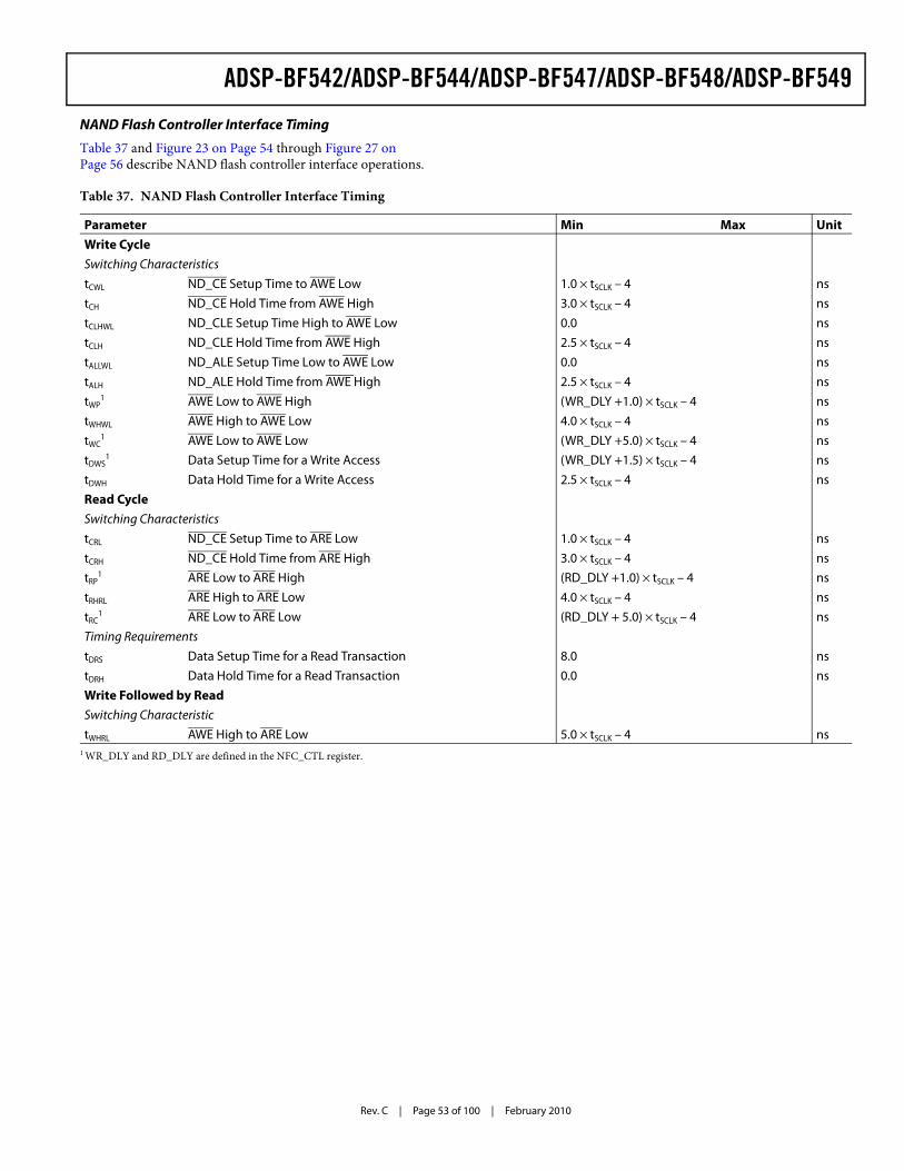
ADSP-BF542/ADSP-BF544/ADSP-BF547/ADSP-BF548/ADSP-BF549
Rev. C | Page 53 of 100 | February 2010
NAND Flash Controller Interface Timing
Table 37 and Figure 23 on Page 54 through Figure 27 on Page 56 describe NAND flash controller interface operations.
Table 37. NAND Flash Controller Interface Timing
Parameter Min Max UnitWrite CycleSwitching Characteristics tCWL ND_CE Setup Time to AWE Low 1.0 × tSCLK – 4 nstCH ND_CE Hold Time from AWE High 3.0 × tSCLK – 4 nstCLHWL ND_CLE Setup Time High to AWE Low 0.0 nstCLH ND_CLE Hold Time from AWE High 2.5 × tSCLK – 4 nstALLWL ND_ALE Setup Time Low to AWE Low 0.0 nstALH ND_ALE Hold Time from AWE High 2.5 × tSCLK – 4 nstWP
1 AWE Low to AWE High (WR_DLY +1.0) × tSCLK – 4 nstWHWL AWE High to AWE Low 4.0 × tSCLK – 4 nstWC
1 AWE Low to AWE Low (WR_DLY +5.0) × tSCLK – 4 nstDWS
1 Data Setup Time for a Write Access (WR_DLY +1.5) × tSCLK – 4 nstDWH Data Hold Time for a Write Access 2.5 × tSCLK – 4 nsRead CycleSwitching Characteristics tCRL ND_CE Setup Time to ARE Low 1.0 × tSCLK – 4 nstCRH ND_CE Hold Time from ARE High 3.0 × tSCLK – 4 nstRP
1 ARE Low to ARE High (RD_DLY +1.0) × tSCLK – 4 nstRHRL ARE High to ARE Low 4.0 × tSCLK – 4 nstRC
1 ARE Low to ARE Low (RD_DLY + 5.0) × tSCLK – 4 nsTiming Requirements tDRS Data Setup Time for a Read Transaction 8.0 nstDRH Data Hold Time for a Read Transaction 0.0 nsWrite Followed by ReadSwitching Characteristic tWHRL AWE High to ARE Low 5.0 × tSCLK – 4 ns
1 WR_DLY and RD_DLY are defined in the NFC_CTL register.
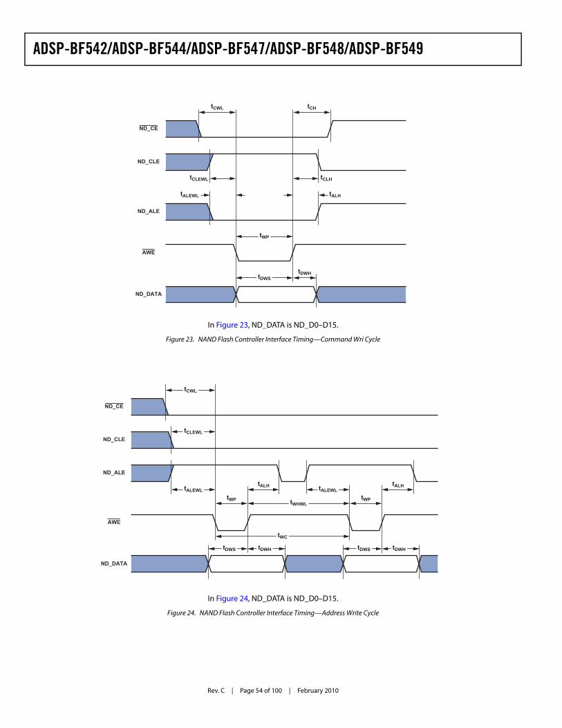
Rev. C | Page 54 of 100 | February 2010
ADSP-BF542/ADSP-BF544/ADSP-BF547/ADSP-BF548/ADSP-BF549
In Figure 23, ND_DATA is ND_D0–D15.
Figure 23. NAND Flash Controller Interface Timing—Command Wri Cycle
tCLEWL
tALEWL
ND_DATA
tCHtCWL
tCLH
tALH
tDWH
ND_CE
ND_CLE
ND_ALE
AWE
tWP
tDWS
In Figure 24, ND_DATA is ND_D0–D15.
Figure 24. NAND Flash Controller Interface Timing—Address Write Cycle
ND_DATA
tWP tWP
tALH tALH
ND_CE
ND_CLE
ND_ALE
AWE
tCWL
tCLEWL
tALEWL
tWHWL
tWC
tDWS tDWH tDWS tDWH
tALEWL
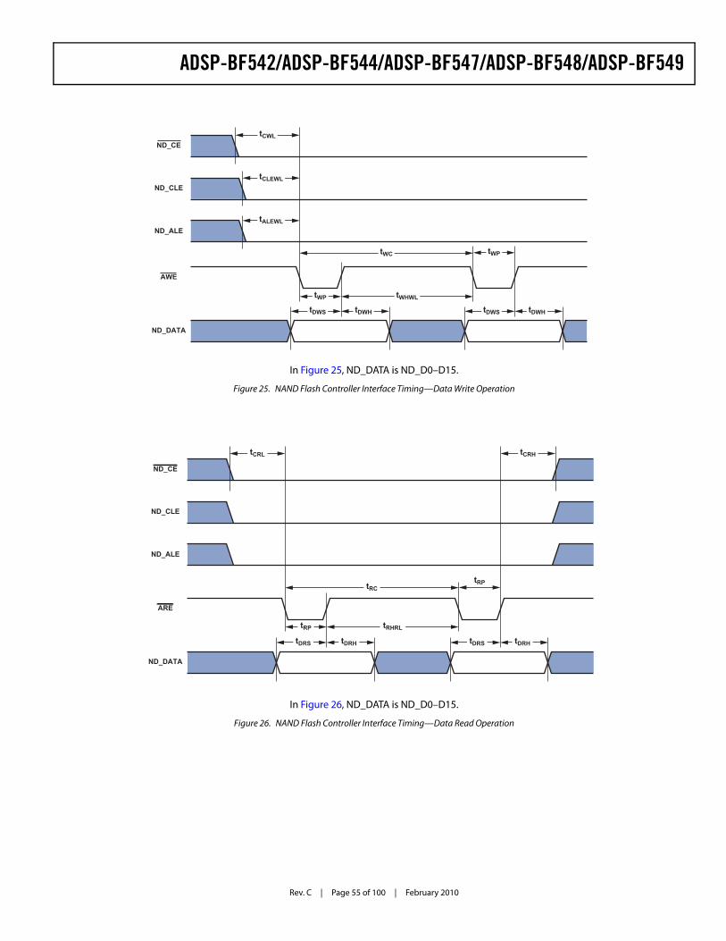
ADSP-BF542/ADSP-BF544/ADSP-BF547/ADSP-BF548/ADSP-BF549
Rev. C | Page 55 of 100 | February 2010
In Figure 25, ND_DATA is ND_D0–D15.
Figure 25. NAND Flash Controller Interface Timing—Data Write Operation
ND_DATA
ND_CE
ND_CLE
ND_ALE
AWE
tCWL
tCLEWL
tALEWL
tWC
tDWS tDWH tDWS tDWH
tWHWLtWP
tWP
In Figure 26, ND_DATA is ND_D0–D15.
Figure 26. NAND Flash Controller Interface Timing—Data Read Operation
ND_DATA
tRP
ND_CLE
ND_CE
ND_ALE
ARE
tCRL tCRH
tRP tRHRL
tRC
tDRS tDRH tDRS tDRH
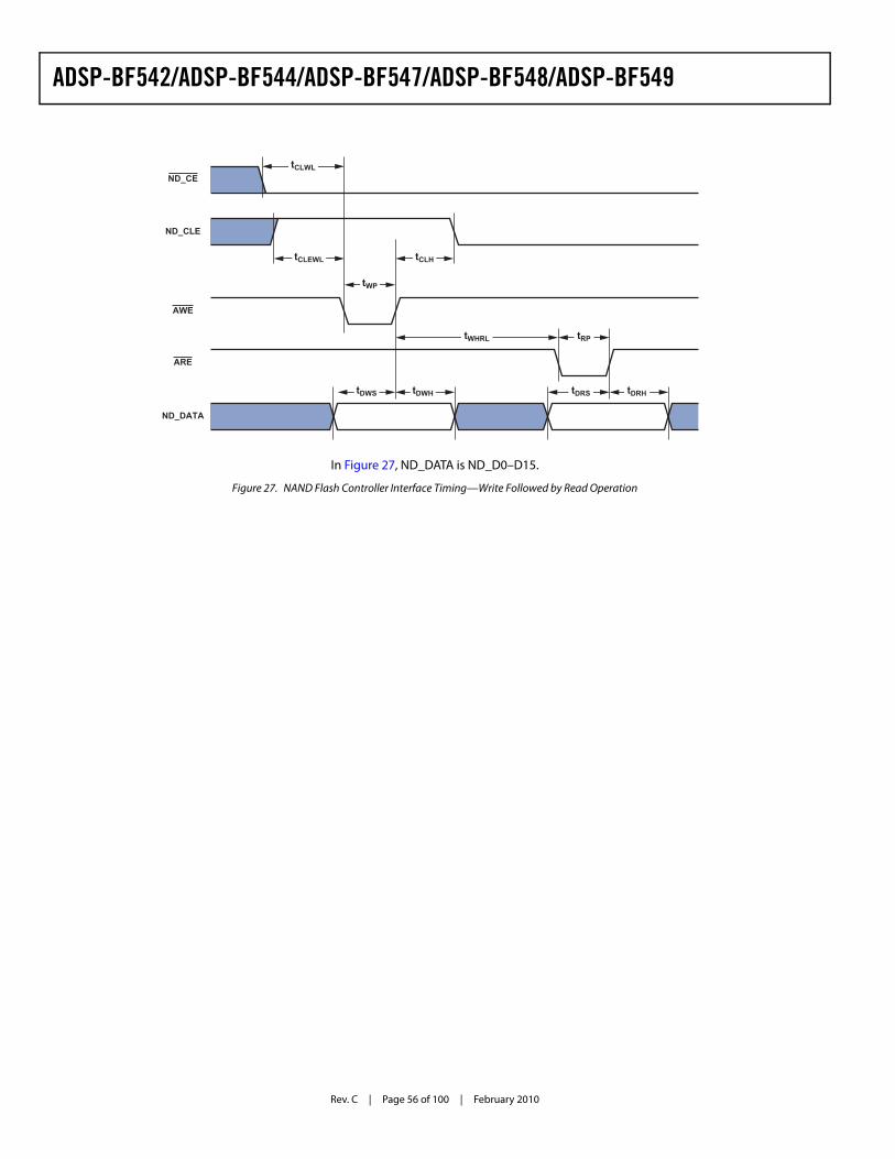
Rev. C | Page 56 of 100 | February 2010
ADSP-BF542/ADSP-BF544/ADSP-BF547/ADSP-BF548/ADSP-BF549
In Figure 27, ND_DATA is ND_D0–D15.
Figure 27. NAND Flash Controller Interface Timing—Write Followed by Read Operation
ND_DATA
ND_CLE
tCLWL
tCLEWL tCLH
ARE
AWE
tDWS tDWH tDRS tDRH
tWHRL
tWP
tRP
ND_CE
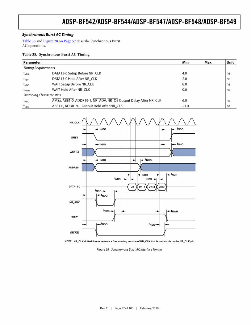
ADSP-BF542/ADSP-BF544/ADSP-BF547/ADSP-BF548/ADSP-BF549
Rev. C | Page 57 of 100 | February 2010
Synchronous Burst AC Timing
Table 38 and Figure 28 on Page 57 describe Synchronous Burst AC operations.
Table 38. Synchronous Burst AC Timing
Parameter Min Max UnitTiming Requirements tNDS DATA15-0 Setup Before NR_CLK 4.0 nstNDH DATA15-0 Hold After NR_CLK 2.0 nstNWS WAIT Setup Before NR_CLK 8.0 nstNWH WAIT Hold After NR_CLK 0.0 nsSwitching Characteristics tNDO AMSx, ABE1-0, ADDR19-1, NR_ADV, NR_OE Output Delay After NR_CLK 6.0 nstNHO ABE1-0, ADDR19-1 Output Hold After NR_CLK –3.0 ns
Figure 28. Synchronous Burst AC Interface Timing
tNDO
tNDO
tNDO
tNDO
tNDO
tNWS tNWH
tNDO
tNDO
tNHO
tNDH tNDH
tNDS tNDS
tNDO
tNHO
Dn Dn+1 Dn+2 Dn+3
AMSx
NR_CLK
ABE1-0
ADDR19-1
DATA15-0
NR_ADV
NR_OE
WAIT
NOTE: NR_CLK dotted line represents a free running version of NR_CLK that is not visible on the NR_CLK pin.
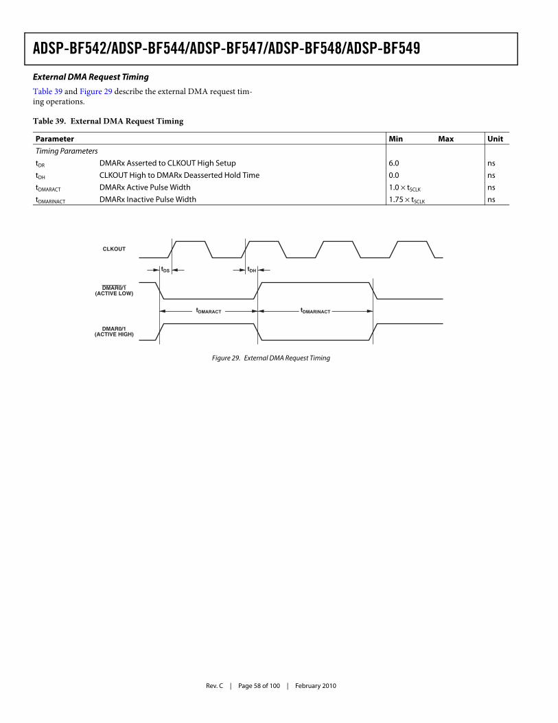
Rev. C | Page 58 of 100 | February 2010
ADSP-BF542/ADSP-BF544/ADSP-BF547/ADSP-BF548/ADSP-BF549
External DMA Request Timing
Table 39 and Figure 29 describe the external DMA request tim-ing operations.
Table 39. External DMA Request Timing
Parameter Min Max UnitTiming ParameterstDR DMARx Asserted to CLKOUT High Setup 6.0 nstDH CLKOUT High to DMARx Deasserted Hold Time 0.0 nstDMARACT DMARx Active Pulse Width 1.0 × tSCLK nstDMARINACT DMARx Inactive Pulse Width 1.75 × tSCLK ns
Figure 29. External DMA Request Timing
CLKOUT
tDS
DMAR0/1(ACTIVE LOW)
DMAR0/1(ACTIVE HIGH)
tDMARACT tDMARINACT
tDH
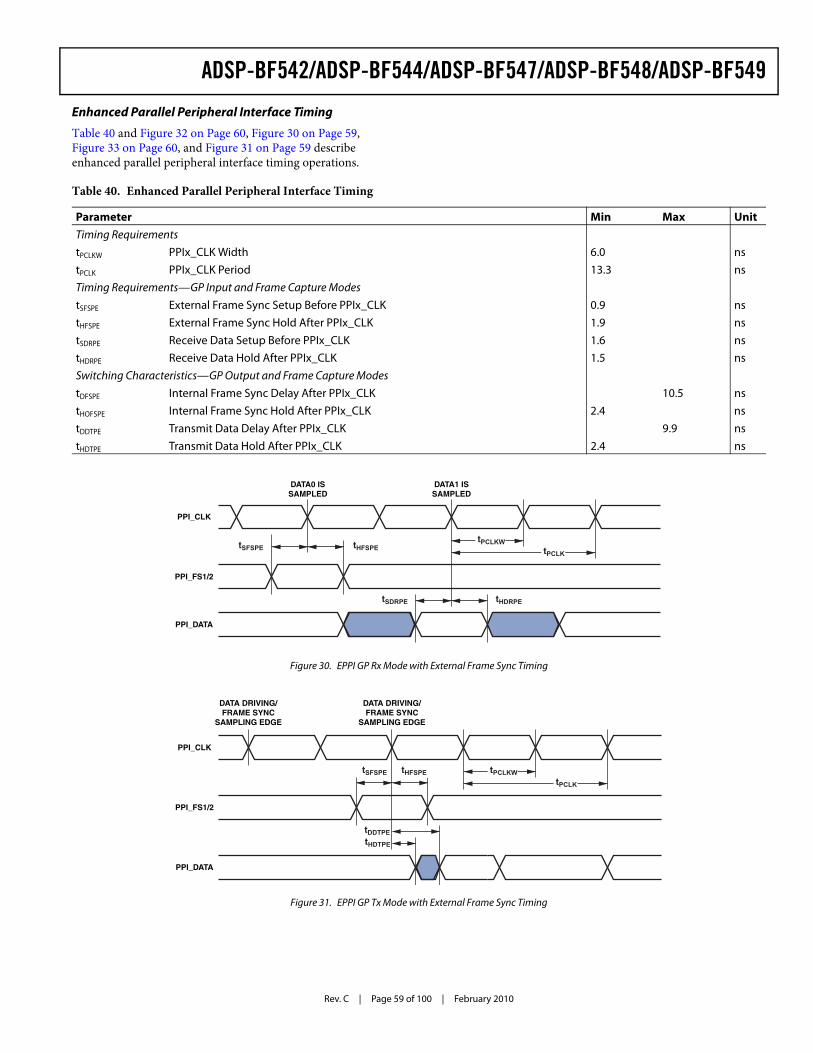
ADSP-BF542/ADSP-BF544/ADSP-BF547/ADSP-BF548/ADSP-BF549
Rev. C | Page 59 of 100 | February 2010
Enhanced Parallel Peripheral Interface Timing
Table 40 and Figure 32 on Page 60, Figure 30 on Page 59, Figure 33 on Page 60, and Figure 31 on Page 59 describe enhanced parallel peripheral interface timing operations.
Table 40. Enhanced Parallel Peripheral Interface Timing
Parameter Min Max UnitTiming RequirementstPCLKW PPIx_CLK Width 6.0 nstPCLK PPIx_CLK Period 13.3 nsTiming Requirements—GP Input and Frame Capture ModestSFSPE External Frame Sync Setup Before PPIx_CLK 0.9 nstHFSPE External Frame Sync Hold After PPIx_CLK 1.9 nstSDRPE Receive Data Setup Before PPIx_CLK 1.6 nstHDRPE Receive Data Hold After PPIx_CLK 1.5 nsSwitching Characteristics—GP Output and Frame Capture ModestDFSPE Internal Frame Sync Delay After PPIx_CLK 10.5 nstHOFSPE Internal Frame Sync Hold After PPIx_CLK 2.4 nstDDTPE Transmit Data Delay After PPIx_CLK 9.9 nstHDTPE Transmit Data Hold After PPIx_CLK 2.4 ns
Figure 30. EPPI GP Rx Mode with External Frame Sync Timing
Figure 31. EPPI GP Tx Mode with External Frame Sync Timing
tPCLKtSFSPE
DATA0 ISSAMPLED
DATA1 ISSAMPLED
PPI_DATA
PPI_CLK
PPI_FS1/2
tHFSPE
tHDRPEtSDRPE
tPCLKW
tHDTPE
tSFSPE
DATA DRIVING/FRAME SYNC
SAMPLING EDGE
DATA DRIVING/FRAME SYNC
SAMPLING EDGE
PPI_DATA
PPI_CLK
PPI_FS1/2
tHFSPE
tDDTPE
tPCLK
tPCLKW
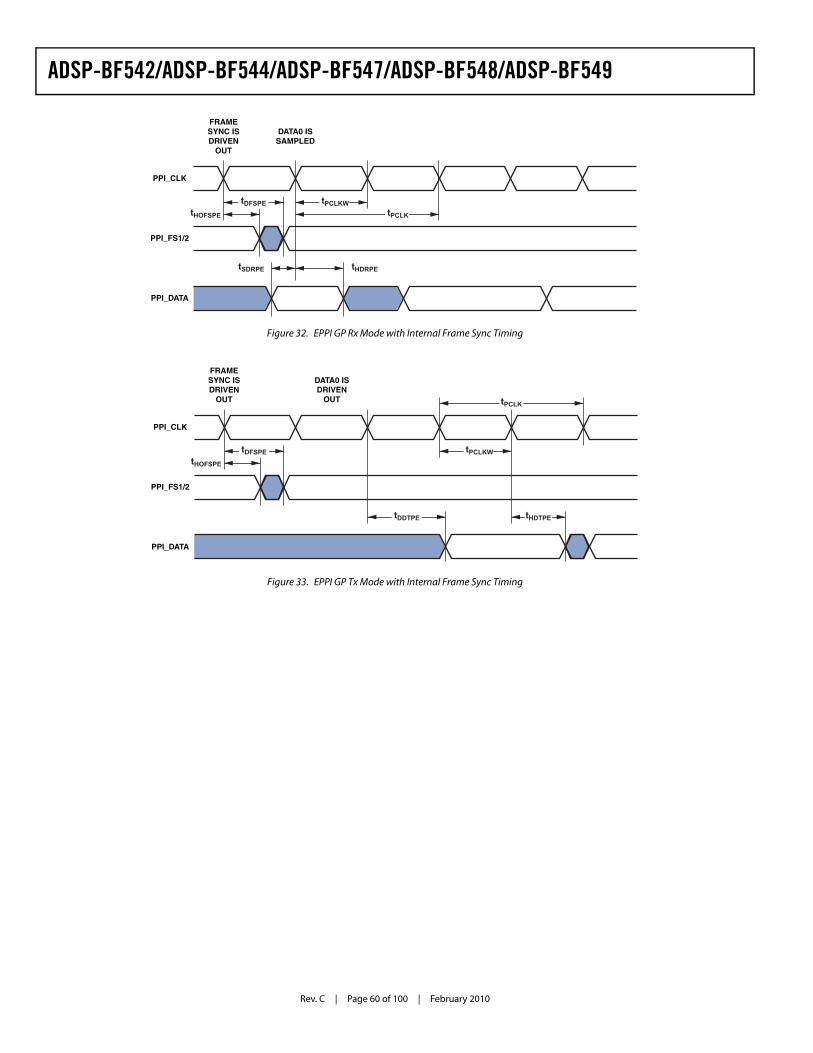
Rev. C | Page 60 of 100 | February 2010
ADSP-BF542/ADSP-BF544/ADSP-BF547/ADSP-BF548/ADSP-BF549
Figure 32. EPPI GP Rx Mode with Internal Frame Sync Timing
Figure 33. EPPI GP Tx Mode with Internal Frame Sync Timing
tHDRPEtSDRPE
tHOFSPE
FRAMESYNC ISDRIVEN
OUT
DATA0 ISSAMPLED
PPI_DATA
PPI_CLK
PPI_FS1/2
tDFSPEtPCLK
tPCLKW
tHOFSPE
FRAMESYNC ISDRIVEN
OUT
DATA0 ISDRIVEN
OUT
PPI_DATA
PPI_CLK
PPI_FS1/2
tDFSPE
tDDTPE tHDTPE
tPCLK
tPCLKW
ADSP-BF542/ADSP-BF544/ADSP-BF547/ADSP-BF548/ADSP-BF549
Rev. C | Page 61 of 100 | February 2010
Serial Ports Timing
Table 41 through Table 44 on Page 63 and Figure 34 on Page 62 through Figure 37 on Page 63 describe serial port operations.
Table 41. Serial Ports—External Clock
Parameter Min Max Unit
Timing Requirements
tSFSE TFSx/RFSx Setup Before TSCLKx/RSCLKx (Externally Generated TFSx/RFSx)1 3.0 ns
tHFSE TFSx/RFSx Hold After TSCLKx/RSCLKx (Externally Generated TFSx/RFSx)1 3.0 ns
tSDRE Receive Data Setup Before RSCLKx1 3.0 ns
tHDRE Receive Data Hold After RSCLKx1 3.0 ns
tSCLKEW TSCLKx/RSCLKx Width 4.5 ns
tSCLKE TSCLKx/RSCLKx Period 15.0 ns
tRCLKE RSCLKx Period2 11.1 ns
tSUDTE Start-Up Delay From SPORT Enable To First External TFSx 4 × tSCLKE ns
tSUDRE Start-Up Delay From SPORT Enable To First External RFSx 4 × tRCLKE ns
Switching Characteristics
tDFSE TFSx/RFSx Delay After TSCLKx/RSCLKx (Internally Generated TFSx/RFSx)3 10.0 ns
tHOFSE TFSx/RFSx Hold After TSCLKx/RSCLKx (Internally Generated TFSx/RFSx)3 0.0 ns
tDDTE Transmit Data Delay After TSCLKx3 10.0 ns
tHDTE Transmit Data Hold After TSCLKx3 0.0 ns1 Referenced to sample edge.2 For serial port receive with external clock and external frame sync only.3 Referenced to drive edge.
Table 42. Serial Ports—Internal Clock
Parameter Min Max Unit
Timing Requirements
tSFSI TFSx/RFSx Setup Before TSCLKx/RSCLKx (Externally Generated TFSx/RFSx)1 10.0 ns
tHFSI TFSx/RFSx Hold After TSCLKx/RSCLKx (Externally Generated TFSx/RFSx)1 –1.5 ns
tSDRI Receive Data Setup Before RSCLKx1 10.0 ns
tHDRI Receive Data Hold After RSCLKx1 –1.5 ns
Switching Characteristics
tDFSI TFSx/RFSx Delay After TSCLKx/RSCLKx (Internally Generated TFSx/RFSx)2 3.0 ns
tHOFSI TFSx/RFSx Hold After TSCLKx/RSCLKx (Internally Generated TFSx/RFSx)2 –1.0 ns
tDDTI Transmit Data Delay After TSCLKx2 3.0 ns
tHDTI Transmit Data Hold After TSCLKx2 –2.0 ns
tSCLKIW TSCLKx/RSCLKx Width 4.5 ns1 Referenced to sample edge.2 Referenced to drive edge.
Rev. C | Page 62 of 100 | February 2010
ADSP-BF542/ADSP-BF544/ADSP-BF547/ADSP-BF548/ADSP-BF549
Figure 34. Serial Port Start-Up with External Clock and Frame Sync
Figure 35. Serial Ports
TSCLKx(INPUT)
TFSx(INPUT)
RFSx(INPUT)
RSCLKx(INPUT)
tSUDTE
tSUDRE
FIRSTTSCLKx/RSCLKx
EDGE AFTER SPORT ENABLED
tSDRI
RSCLKx
DRx
DRIVE EDGE
tHDRI
tSFSI tHFSI
tDFSItHOFSI
tSCLKIW
DATA RECEIVE—INTERNAL CLOCK
tSDRE
DATA RECEIVE—EXTERNAL CLOCK
RSCLKx
DRx
tHDRE
tSFSE tHFSE
tDFSE
tSCLKEW
tHOFSE
tDDTI
tHDTI
TSCLKx
TFSx(INPUT)
DTx
tSFSI tHFSI
tSCLKIW
tD FSI
tHOFSI
DATA TRANSMIT—INTERNAL CLOCK
tDDTE
tHDTE
TSCLKx
DTx
tSFSE
tDFSE
t SCLKEW
tHOFSE
DATA TRANSMIT—EXTERNAL CLOCK
SAMPLE EDGE
DRIVE EDGE SAMPLE EDGE DRIVE EDGE SAMPLE EDGE
DRIVE EDGE SAMPLE EDGEtSCLKE
tSCLKE
tHFSE
TFSx(OUTPUT)
TFSx(INPUT)
TFSx(OUTPUT)
RFSx(INPUT)
RFSx(OUTPUT)
RFSx(INPUT)
RFSx(OUTPUT)
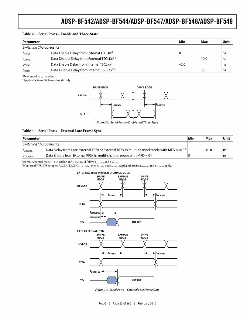
ADSP-BF542/ADSP-BF544/ADSP-BF547/ADSP-BF548/ADSP-BF549
Rev. C | Page 63 of 100 | February 2010
Table 43. Serial Ports—Enable and Three-State
Parameter Min Max Unit
Switching Characteristics
tDTENE Data Enable Delay from External TSCLKx1 0 ns
tDDTTE Data Disable Delay from External TSCLKx1, 2 10.0 ns
tDTENI Data Enable Delay from Internal TSCLKx1 –2.0 ns
tDDTTI Data Disable Delay from Internal TSCLKx1, 2 3.0 ns1 Referenced to drive edge.2 Applicable to multichannel mode only.
Figure 36. Serial Ports—Enable and Three-State
Table 44. Serial Ports—External Late Frame Sync
Parameter Min Max Unit
Switching Characteristics
tDDTLFSE Data Delay from Late External TFSx or External RFSx in multi-channel mode with MFD = 011, 2 10.0 ns
tDTENLFSE Data Enable from External RFSx in multi-channel mode with MFD = 01, 2 0 ns1 In multichannel mode, TFSx enable and TFSx valid follow tDTENLFS and tDDTLFSE.2 If external RFS/TFS setup to RSCLK/TSCLK > tSCLKE/2, then tDDTE/I and tDTENE/I apply; otherwise tDDTLFSE and tDTENLFS apply.
Figure 37. Serial Ports—External Late Frame Sync
TSCLKx
DTx
DRIVE EDGE
tDDTTE/ItDTENE/I
DRIVE EDGE
RSCLKx
RFSx
DTx
DRIVEEDGE
DRIVEEDGE
SAMPLEEDGE
EXTERNAL RFSx IN MULTI-CHANNEL MODE
1ST BIT
tHOFSE/I
tDTENLFSE
tDDTLFSE
tSFSE/I
TSCLKx
TFSx
DTx
DRIVEEDGE
DRIVEEDGE
SAMPLEEDGE
LATE EXTERNAL TFSx
1ST BIT
tHOFSE/I
tDDTLFSE
tSFSE/I
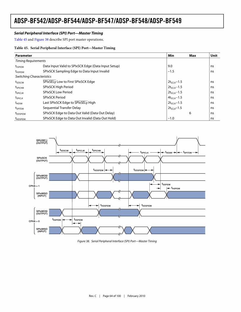
Rev. C | Page 64 of 100 | February 2010
ADSP-BF542/ADSP-BF544/ADSP-BF547/ADSP-BF548/ADSP-BF549
Serial Peripheral Interface (SPI) Port—Master Timing
Table 45 and Figure 38 describe SPI port master operations.
Table 45. Serial Peripheral Interface (SPI) Port—Master Timing
Parameter Min Max UnitTiming RequirementstSSPIDM Data Input Valid to SPIxSCK Edge (Data Input Setup) 9.0 nstHSPIDM SPIxSCK Sampling Edge to Data Input Invalid –1.5 nsSwitching CharacteristicstSDSCIM SPIxSELy Low to First SPIxSCK Edge 2tSCLK –1.5 nstSPICHM SPIxSCK High Period 2tSCLK –1.5 nstSPICLM SPIxSCK Low Period 2tSCLK –1.5 nstSPICLK SPIxSCK Period 4tSCLK –1.5 nstHDSM Last SPIxSCK Edge to SPIxSELy High 2tSCLK –1.5 nstSPITDM Sequential Transfer Delay 2tSCLK–1.5 nstDDSPIDM SPIxSCK Edge to Data Out Valid (Data Out Delay) 6 nstHDSPIDM SPIxSCK Edge to Data Out Invalid (Data Out Hold) –1.0 ns
Figure 38. Serial Peripheral Interface (SPI) Port—Master Timing
tSDSCIM tSPICLK tHDSM tSPITDMtSPICLM tSPICHM
tHDSPIDM
tHSPIDMtSSPIDM
SPIxSELy(OUTPUT)
SPIxSCK(OUTPUT)
SPIxMOSI(OUTPUT)
SPIxMISO(INPUT)
SPIxMOSI(OUTPUT)
SPIxMISO(INPUT)
CPHA = 1
CPHA = 0
tDDSPIDM
tHSPIDM
tSSPIDM
tHDSPIDM
tDDSPIDM
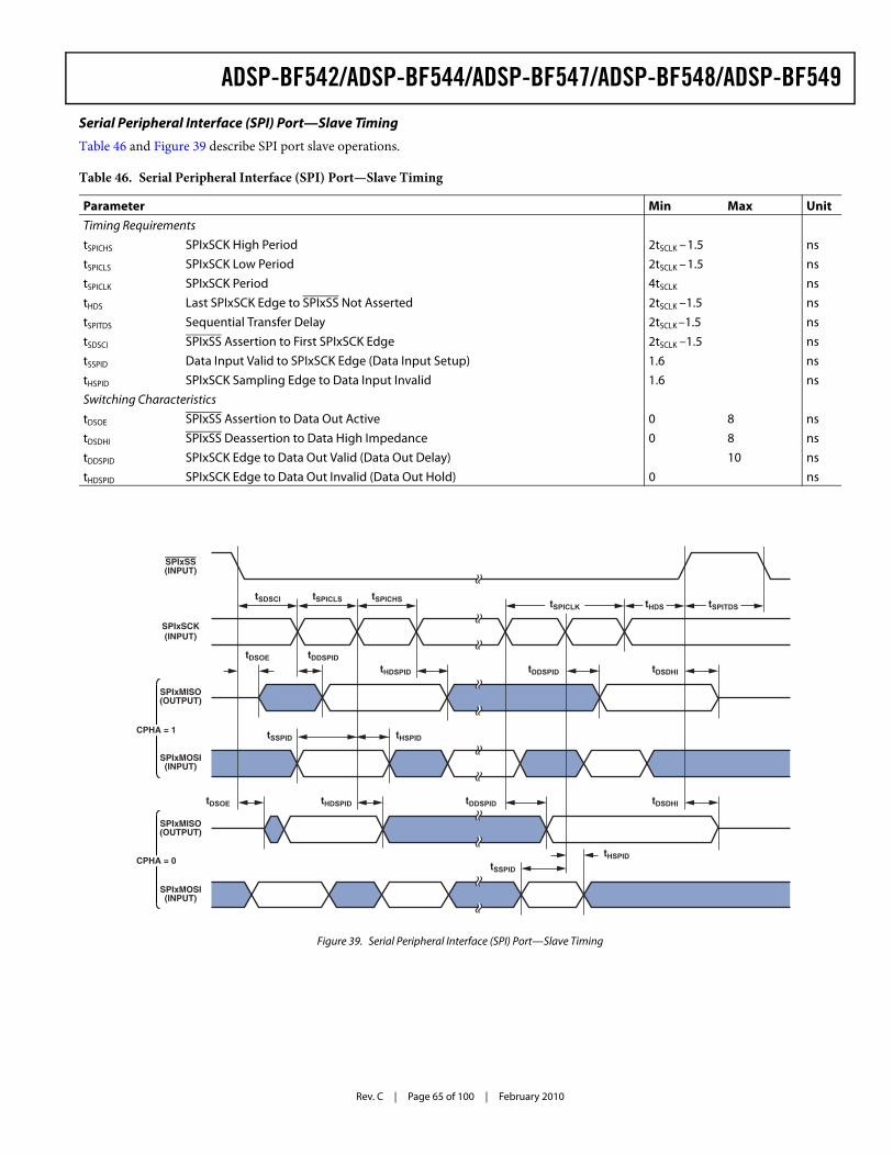
ADSP-BF542/ADSP-BF544/ADSP-BF547/ADSP-BF548/ADSP-BF549
Rev. C | Page 65 of 100 | February 2010
Serial Peripheral Interface (SPI) Port—Slave Timing
Table 46 and Figure 39 describe SPI port slave operations.
Table 46. Serial Peripheral Interface (SPI) Port—Slave Timing
Parameter Min Max UnitTiming RequirementstSPICHS SPIxSCK High Period 2tSCLK –1.5 nstSPICLS SPIxSCK Low Period 2tSCLK –1.5 nstSPICLK SPIxSCK Period 4tSCLK nstHDS Last SPIxSCK Edge to SPIxSS Not Asserted 2tSCLK –1.5 nstSPITDS Sequential Transfer Delay 2tSCLK –1.5 nstSDSCI SPIxSS Assertion to First SPIxSCK Edge 2tSCLK –1.5 nstSSPID Data Input Valid to SPIxSCK Edge (Data Input Setup) 1.6 nstHSPID SPIxSCK Sampling Edge to Data Input Invalid 1.6 nsSwitching CharacteristicstDSOE SPIxSS Assertion to Data Out Active 0 8 nstDSDHI SPIxSS Deassertion to Data High Impedance 0 8 nstDDSPID SPIxSCK Edge to Data Out Valid (Data Out Delay) 10 nstHDSPID SPIxSCK Edge to Data Out Invalid (Data Out Hold) 0 ns
Figure 39. Serial Peripheral Interface (SPI) Port—Slave Timing
tSPICLK tHDS tSPITDStSDSCI tSPICLS tSPICHS
tDSOE tDDSPIDtDDSPID tDSDHItHDSPID
tSSPID
tDSDHItHDSPIDtDSOE
tHSPIDtSSPID
tDDSPID
SPIxSS(INPUT)
SPIxSCK(INPUT)
SPIxMISO(OUTPUT)
SPIxMOSI(INPUT)
SPIxMISO(OUTPUT)
SPIxMOSI(INPUT)
CPHA = 1
CPHA = 0
tHSPID
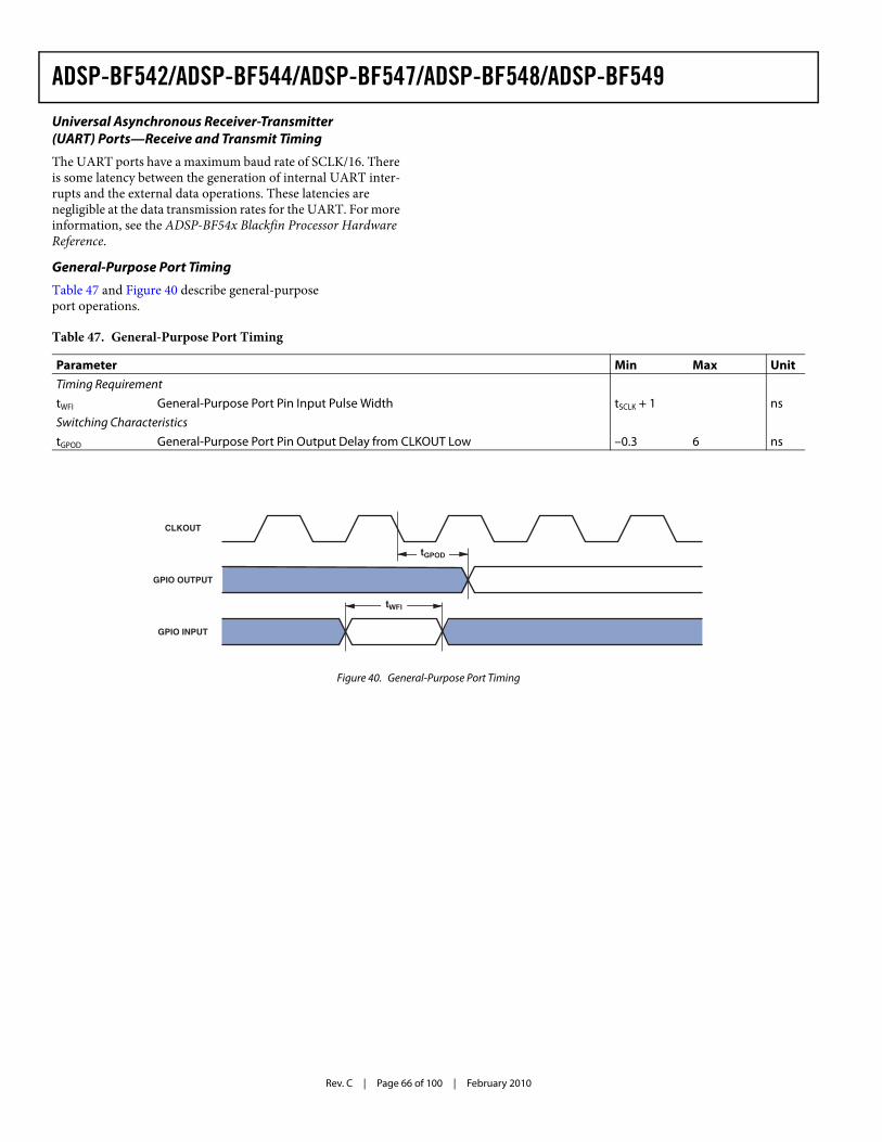
Rev. C | Page 66 of 100 | February 2010
ADSP-BF542/ADSP-BF544/ADSP-BF547/ADSP-BF548/ADSP-BF549
Universal Asynchronous Receiver-Transmitter (UART) Ports—Receive and Transmit Timing
The UART ports have a maximum baud rate of SCLK/16. There is some latency between the generation of internal UART inter-rupts and the external data operations. These latencies are negligible at the data transmission rates for the UART. For more information, see the ADSP-BF54x Blackfin Processor Hardware Reference.
General-Purpose Port Timing
Table 47 and Figure 40 describe general-purpose port operations.
Table 47. General-Purpose Port Timing
Parameter Min Max UnitTiming RequirementtWFI General-Purpose Port Pin Input Pulse Width tSCLK + 1 nsSwitching CharacteristicstGPOD General-Purpose Port Pin Output Delay from CLKOUT Low –0.3 6 ns
Figure 40. General-Purpose Port Timing
CLKOUT
GPIO OUTPUT
GPIO INPUT
tWFI
tGPOD
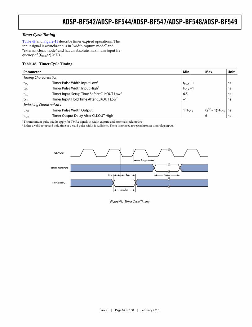
ADSP-BF542/ADSP-BF544/ADSP-BF547/ADSP-BF548/ADSP-BF549
Rev. C | Page 67 of 100 | February 2010
Timer Cycle Timing
Table 48 and Figure 41 describe timer expired operations. The input signal is asynchronous in “width capture mode” and “external clock mode” and has an absolute maximum input fre-quency of (fSCLK/2) MHz.
Table 48. Timer Cycle Timing
Parameter Min Max UnitTiming CharacteristicstWL Timer Pulse Width Input Low1 tSCLK +1 nstWH Timer Pulse Width Input High1 tSCLK +1 nstTIS Timer Input Setup Time Before CLKOUT Low2 6.5 nstTIH Timer Input Hold Time After CLKOUT Low2 –1 nsSwitching CharacteristicstHTO Timer Pulse Width Output 1×tSCLK (232 – 1)×tSCLK nstTOD Timer Output Delay After CLKOUT High 6 ns
1 The minimum pulse widths apply for TMRx signals in width capture and external clock modes.2 Either a valid setup and hold time or a valid pulse width is sufficient. There is no need to resynchronize timer flag inputs.
Figure 41. Timer Cycle Timing
CLKOUT
TMRx OUTPUT
TMRx INPUT
tTIS tTIH
tWH,tWL
tTOD
tHTO
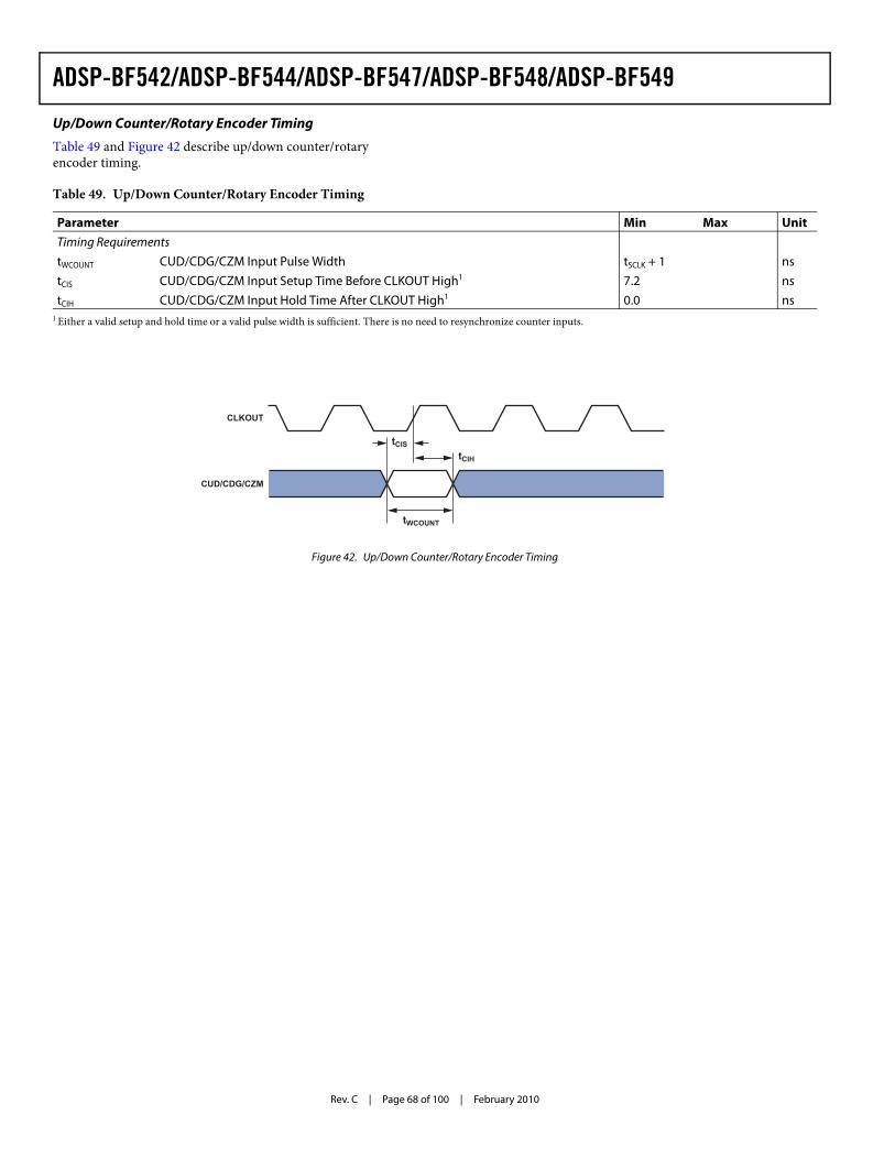
Rev. C | Page 68 of 100 | February 2010
ADSP-BF542/ADSP-BF544/ADSP-BF547/ADSP-BF548/ADSP-BF549
Up/Down Counter/Rotary Encoder Timing
Table 49 and Figure 42 describe up/down counter/rotary encoder timing.
Table 49. Up/Down Counter/Rotary Encoder Timing
Parameter Min Max UnitTiming RequirementstWCOUNT CUD/CDG/CZM Input Pulse Width tSCLK + 1 nstCIS CUD/CDG/CZM Input Setup Time Before CLKOUT High1 7.2 nstCIH CUD/CDG/CZM Input Hold Time After CLKOUT High1 0.0 ns
1 Either a valid setup and hold time or a valid pulse width is sufficient. There is no need to resynchronize counter inputs.
Figure 42. Up/Down Counter/Rotary Encoder Timing
CLKOUT
CUD/CDG/CZM
tCIStCIH
tWCOUNT
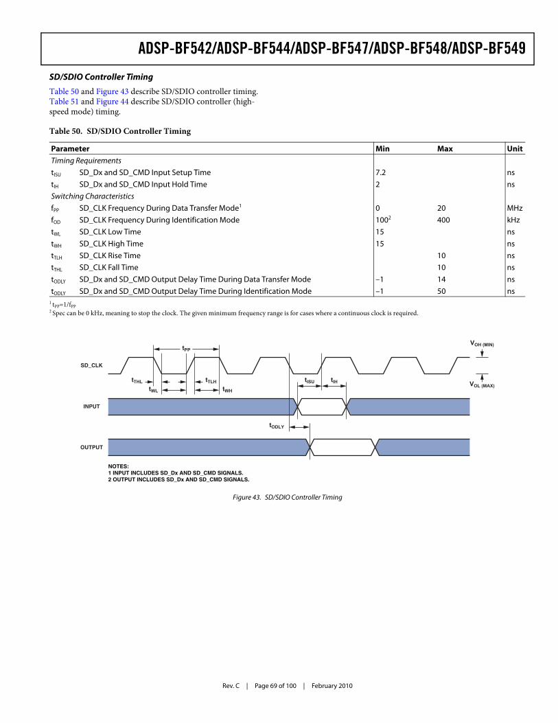
ADSP-BF542/ADSP-BF544/ADSP-BF547/ADSP-BF548/ADSP-BF549
Rev. C | Page 69 of 100 | February 2010
SD/SDIO Controller Timing
Table 50 and Figure 43 describe SD/SDIO controller timing. Table 51 and Figure 44 describe SD/SDIO controller (high-speed mode) timing.
Table 50. SD/SDIO Controller Timing
Parameter Min Max UnitTiming RequirementstISU SD_Dx and SD_CMD Input Setup Time 7.2 nstIH SD_Dx and SD_CMD Input Hold Time 2 nsSwitching CharacteristicsfPP SD_CLK Frequency During Data Transfer Mode1 0 20 MHzfOD SD_CLK Frequency During Identification Mode 1002 400 kHztWL SD_CLK Low Time 15 nstWH SD_CLK High Time 15 nstTLH SD_CLK Rise Time 10 nstTHL SD_CLK Fall Time 10 nstODLY SD_Dx and SD_CMD Output Delay Time During Data Transfer Mode –1 14 nstODLY SD_Dx and SD_CMD Output Delay Time During Identification Mode –1 50 ns
1 tPP=1/fPP2 Spec can be 0 kHz, meaning to stop the clock. The given minimum frequency range is for cases where a continuous clock is required.
Figure 43. SD/SDIO Controller Timing
SD_CLK
INPUT
OUTPUT
tISU
NOTES:1 INPUT INCLUDES SD_Dx AND SD_CMD SIGNALS.2 OUTPUT INCLUDES SD_Dx AND SD_CMD SIGNALS.
tTHL tTLHtWL tWH
tPP
tIH
tODLY
VOH (MIN)
VOL (MAX)
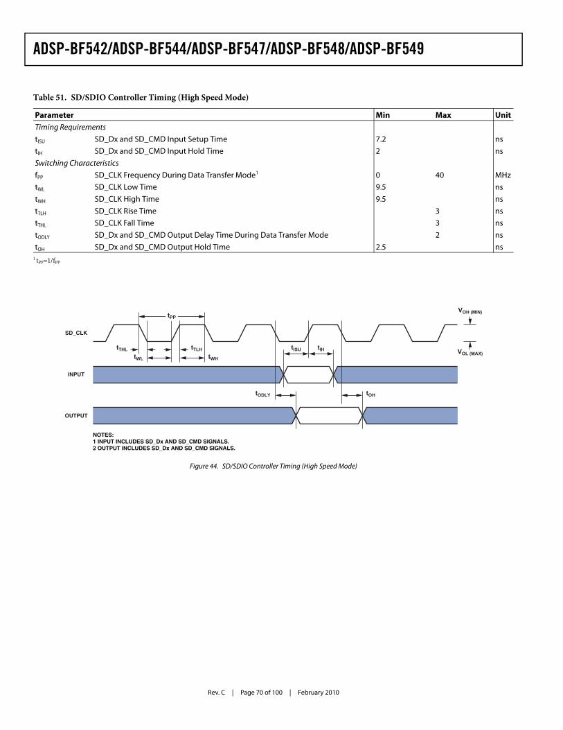
Rev. C | Page 70 of 100 | February 2010
ADSP-BF542/ADSP-BF544/ADSP-BF547/ADSP-BF548/ADSP-BF549
Table 51. SD/SDIO Controller Timing (High Speed Mode)
Parameter Min Max UnitTiming RequirementstISU SD_Dx and SD_CMD Input Setup Time 7.2 nstIH SD_Dx and SD_CMD Input Hold Time 2 nsSwitching CharacteristicsfPP SD_CLK Frequency During Data Transfer Mode1 0 40 MHztWL SD_CLK Low Time 9.5 nstWH SD_CLK High Time 9.5 nstTLH SD_CLK Rise Time 3 nstTHL SD_CLK Fall Time 3 nstODLY SD_Dx and SD_CMD Output Delay Time During Data Transfer Mode 2 nstOH SD_Dx and SD_CMD Output Hold Time 2.5 ns
1 tPP=1/fPP
Figure 44. SD/SDIO Controller Timing (High Speed Mode)
SD_CLK
INPUT
OUTPUT
tISU
NOTES:1 INPUT INCLUDES SD_Dx AND SD_CMD SIGNALS.2 OUTPUT INCLUDES SD_Dx AND SD_CMD SIGNALS.
tTHL tTLHtWL tWH
tPP
tIH
tODLY tOH
VOH (MIN)
VOL (MAX)
ADSP-BF542/ADSP-BF544/ADSP-BF547/ADSP-BF548/ADSP-BF549
Rev. C | Page 71 of 100 | February 2010
MXVR Timing
Table 52 and Table 53 describe the MXVR timing requirements. Figure 5 illustrates the MOST connection.
Table 52. MXVR Timing—MXI Center Frequency Requirements
Parameter Fs = 38 kHz Fs = 44.1 kHz Fs = 48 kHz UnitfMXI_256 MXI Center Frequency (256 Fs) 9.728 11.2896 12.288 MHzfMXI_384 MXI Center Frequency (384 Fs) 14.592 16.9344 18.432 MHzfMXI_512 MXI Center Frequency (512 Fs) 19.456 22.5792 24.576 MHzfMXI_1024 MXI Center Frequency (1024 Fs) 38.912 45.1584 49.152 MHz
Table 53. MXVR Timing— MXI Clock Requirements
Parameter Min Max UnitTiming RequirementsFSMXI MXI Clock Frequency Stability –50 +50 ppmFTMXI MXI Frequency Tolerance Over Temperature –300 +300 ppmDCMXI MXI Clock Duty Cycle +40 +60 %
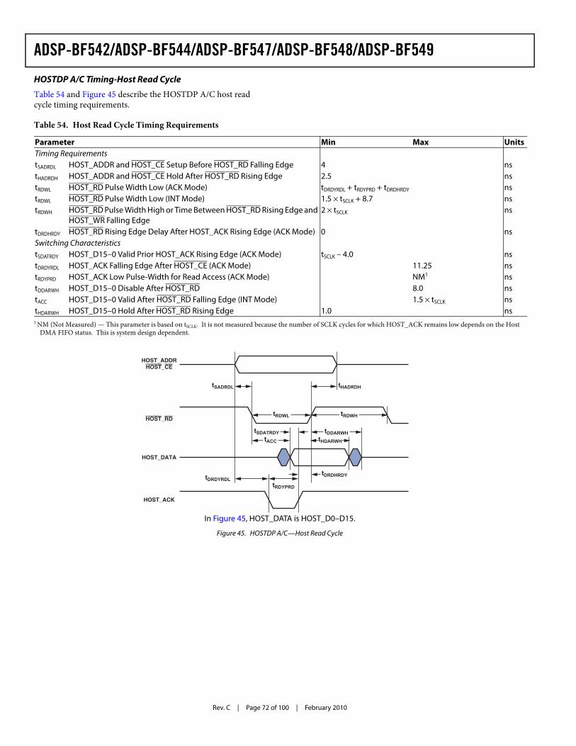
Rev. C | Page 72 of 100 | February 2010
ADSP-BF542/ADSP-BF544/ADSP-BF547/ADSP-BF548/ADSP-BF549
HOSTDP A/C Timing-Host Read Cycle
Table 54 and Figure 45 describe the HOSTDP A/C host read cycle timing requirements.
Table 54. Host Read Cycle Timing Requirements
Parameter Min Max UnitsTiming RequirementstSADRDL HOST_ADDR and HOST_CE Setup Before HOST_RD Falling Edge 4 nstHADRDH HOST_ADDR and HOST_CE Hold After HOST_RD Rising Edge 2.5 nstRDWL HOST_RD Pulse Width Low (ACK Mode) tDRDYRDL + tRDYPRD + tDRDHRDY nstRDWL HOST_RD Pulse Width Low (INT Mode) 1.5 × tSCLK + 8.7 nstRDWH HOST_RD Pulse Width High or Time Between HOST_RD Rising Edge and
HOST_WR Falling Edge2 × tSCLK ns
tDRDHRDY HOST_RD Rising Edge Delay After HOST_ACK Rising Edge (ACK Mode) 0 nsSwitching CharacteristicstSDATRDY HOST_D15–0 Valid Prior HOST_ACK Rising Edge (ACK Mode) tSCLK – 4.0 nstDRDYRDL HOST_ACK Falling Edge After HOST_CE (ACK Mode) 11.25 nstRDYPRD HOST_ACK Low Pulse-Width for Read Access (ACK Mode) NM1 nstDDARWH HOST_D15–0 Disable After HOST_RD 8.0 nstACC HOST_D15–0 Valid After HOST_RD Falling Edge (INT Mode) 1.5 × tSCLK nstHDARWH HOST_D15–0 Hold After HOST_RD Rising Edge 1.0 ns1 NM (Not Measured) — This parameter is based on tSCLK. It is not measured because the number of SCLK cycles for which HOST_ACK remains low depends on the Host
DMA FIFO status. This is system design dependent.
In Figure 45, HOST_DATA is HOST_D0–D15.
Figure 45. HOSTDP A/C—Host Read Cycle
HOST_RD
HOST_ACK
HOST_DATA
tSADRDL tHADRDH
tDRDHRDY
tHDARWH
tRDYPRD
tDRDYRDL
tSDATRDY
HOST_ADDRHOST_CE
tRDWL tRDWH
tACC
tDDARWH
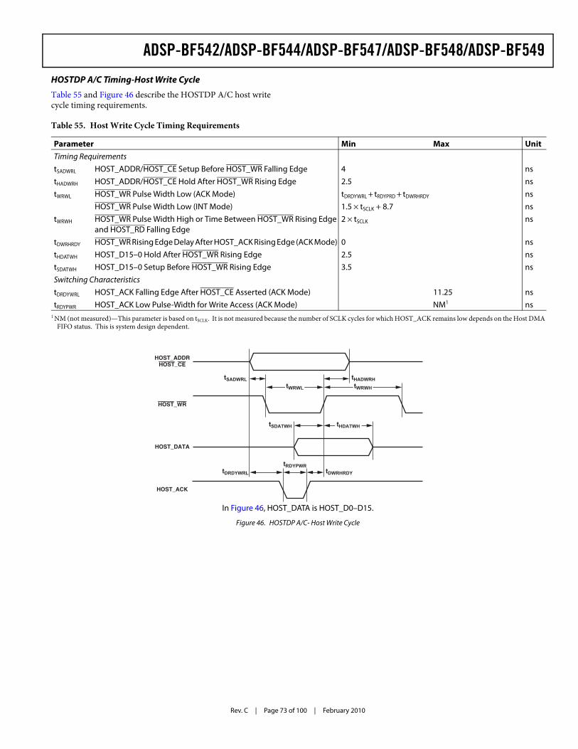
ADSP-BF542/ADSP-BF544/ADSP-BF547/ADSP-BF548/ADSP-BF549
Rev. C | Page 73 of 100 | February 2010
HOSTDP A/C Timing-Host Write Cycle
Table 55 and Figure 46 describe the HOSTDP A/C host write cycle timing requirements.
Table 55. Host Write Cycle Timing Requirements
Parameter Min Max UnitTiming RequirementstSADWRL HOST_ADDR/HOST_CE Setup Before HOST_WR Falling Edge 4 nstHADWRH HOST_ADDR/HOST_CE Hold After HOST_WR Rising Edge 2.5 nstWRWL HOST_WR Pulse Width Low (ACK Mode) tDRDYWRL + tRDYPRD + tDWRHRDY ns
HOST_WR Pulse Width Low (INT Mode) 1.5 × tSCLK + 8.7 nstWRWH HOST_WR Pulse Width High or Time Between HOST_WR Rising Edge
and HOST_RD Falling Edge2 × tSCLK ns
tDWRHRDY HOST_WR Rising Edge Delay After HOST_ACK Rising Edge (ACK Mode) 0 nstHDATWH HOST_D15–0 Hold After HOST_WR Rising Edge 2.5 nstSDATWH HOST_D15–0 Setup Before HOST_WR Rising Edge 3.5 nsSwitching CharacteristicstDRDYWRL HOST_ACK Falling Edge After HOST_CE Asserted (ACK Mode) 11.25 nstRDYPWR HOST_ACK Low Pulse-Width for Write Access (ACK Mode) NM1 ns
1 NM (not measured)—This parameter is based on tSCLK. It is not measured because the number of SCLK cycles for which HOST_ACK remains low depends on the Host DMA FIFO status. This is system design dependent.
In Figure 46, HOST_DATA is HOST_D0–D15.
Figure 46. HOSTDP A/C- Host Write Cycle
HOST_WR
HOST_ACK
HOST_DATA
tSADWRL tHADWRH
tDWRHRDY
tRDYPWRtDRDYWRL
tSDATWH
HOST_ADDRHOST_CE
tWRWL tWRWH
tHDATWH
Rev. C | Page 74 of 100 | February 2010
ADSP-BF542/ADSP-BF544/ADSP-BF547/ADSP-BF548/ADSP-BF549
ATA/ATAPI-6 Interface Timing
The following tables and figures specify ATAPI timing parame-ters. For detailed parameter descriptions, refer to the ATAPI specification (ANSI INCITS 361-2002). Table 58 to Table 61 include ATAPI timing parameter equations. System designers should use these equations along with the parameters provided
in Table 56 and Table 57. ATAPI timing control registers should be programmed such that ANSI INCITS 361-2002 speci-fications are met for the desired transfer type and mode.
Table 56. ATA/ATAPI-6 Timing Parameters
Parameter Min Max UnittSK1 Difference in output delay after CLKOUT for ATAPI output pins1 6 nstOD Output delay after CLKOUT for outputs1 12 nstSUD ATAPI_D0-15 or ATAPI_D0-15A Setup Before CLKOUT 6 nstSUI ATAPI_IORDY Setup Before CLKOUT 6 nstSUDU ATAPI_D0-15 or ATAPI_D0-15A Setup Before ATAPI_IORDY (UDMA-in only) 2 nstHDU ATAPI_D0-15 or ATAPI_D0-15A Hold After ATAPI_IORDY (UDMA-in only) 2.6 ns
1 ATAPI output pins include ATAPI_CS0, ATAPI_CS1, A1-3, ATAPI_DIOR, ATAPI_DIOW, ATAPI_DMACK, ATAPI_D0-15, ATAPI_A0-2A, and ATAPI_D0-15A.
Table 57. ATA/ATAPI-6 System Timing Parameters
Parameter SourcetSK2 Maximum difference in board propagation delay between any 2 ATAPI output pins1 System DesigntBD Maximum board propagation delay. System DesigntSK3 Maximum difference in board propagation delay during a read between ATAPI_IORDY and ATAPI_D0-
15/ATAPI_D0-15A.System Design
tSK4 Maximum difference in ATAPI cable propagation delay between output pin group A and output pin group B2
ATAPI Cable Specification
tCDD ATAPI cable propagation delay for ATAPI_D0-15 and ATAPI_D0-15A signals. ATAPI Cable SpecificationtCDC ATAPI cable propagation delay for ATAPI_DIOR, ATAPI_DIOW, ATAPI_IORDY, and ATAPI_DMACK signals. ATAPI Cable Specification
1 ATAPI output pins include ATAPI_CS0, ATAPI_CS1, A1-3, ATAPI_DIOR, ATAPI_DIOW, ATAPI_DMACK, ATAPI_D0-15, ATAPI_A0-2A, and ATAPI_D0-15A.2 Output pin group A includes ATAPI_DIOR, ATAPI_DIOW, and ATAPI_DMACK. Output pin group B includes ATAPI_CS0, ATAPI_CS1, A1-3, ATAPI_D0-15,
ATAPI_A0-2A, and ATAPI_D0-15A.
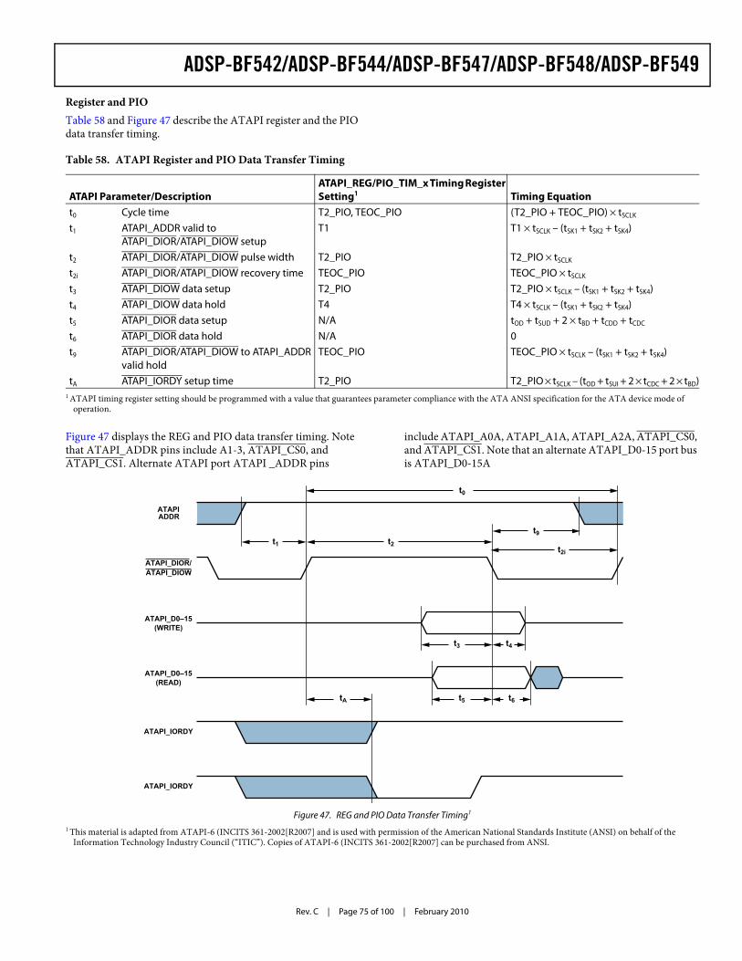
ADSP-BF542/ADSP-BF544/ADSP-BF547/ADSP-BF548/ADSP-BF549
Rev. C | Page 75 of 100 | February 2010
Register and PIO Table 58 and Figure 47 describe the ATAPI register and the PIO data transfer timing.
Figure 47 displays the REG and PIO data transfer timing. Note that ATAPI_ADDR pins include A1-3, ATAPI_CS0, and ATAPI_CS1. Alternate ATAPI port ATAPI _ADDR pins
include ATAPI_A0A, ATAPI_A1A, ATAPI_A2A, ATAPI_CS0, and ATAPI_CS1. Note that an alternate ATAPI_D0-15 port bus is ATAPI_D0-15A
Table 58. ATAPI Register and PIO Data Transfer Timing
ATAPI Parameter/DescriptionATAPI_REG/PIO_TIM_x Timing Register Setting1 Timing Equation
t0 Cycle time T2_PIO, TEOC_PIO (T2_PIO + TEOC_PIO) × tSCLK
t1 ATAPI_ADDR valid to ATAPI_DIOR/ATAPI_DIOW setup
T1 T1 × tSCLK – (tSK1 + tSK2 + tSK4)
t2 ATAPI_DIOR/ATAPI_DIOW pulse width T2_PIO T2_PIO × tSCLK
t2i ATAPI_DIOR/ATAPI_DIOW recovery time TEOC_PIO TEOC_PIO × tSCLK
t3 ATAPI_DIOW data setup T2_PIO T2_PIO × tSCLK – (tSK1 + tSK2 + tSK4)t4 ATAPI_DIOW data hold T4 T4 × tSCLK – (tSK1 + tSK2 + tSK4)t5 ATAPI_DIOR data setup N/A tOD + tSUD + 2 × tBD + tCDD + tCDC
t6 ATAPI_DIOR data hold N/A 0t9 ATAPI_DIOR/ATAPI_DIOW to ATAPI_ADDR
valid holdTEOC_PIO TEOC_PIO × tSCLK – (tSK1 + tSK2 + tSK4)
tA ATAPI_IORDY setup time T2_PIO T2_PIO × tSCLK – (tOD + tSUI + 2 × tCDC + 2 × tBD)1 ATAPI timing register setting should be programmed with a value that guarantees parameter compliance with the ATA ANSI specification for the ATA device mode of
operation.
Figure 47. REG and PIO Data Transfer Timing1
1 This material is adapted from ATAPI-6 (INCITS 361-2002[R2007] and is used with permission of the American National Standards Institute (ANSI) on behalf of the Information Technology Industry Council (“ITIC”). Copies of ATAPI-6 (INCITS 361-2002[R2007] can be purchased from ANSI.
ATAPIADDR
t0
t2
t9
t3 t4
t5tA t6
t2it1
ATAPI_DIOR/ATAPI_DIOW
ATAPI_D0–15
ATAPI_IORDY
ATAPI_IORDY
ATAPI_D0–15(WRITE)
(READ)
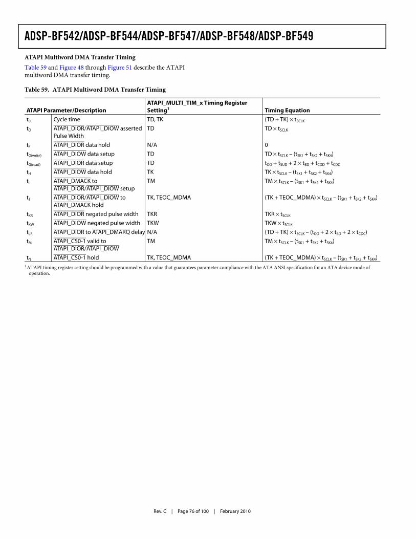
Rev. C | Page 76 of 100 | February 2010
ADSP-BF542/ADSP-BF544/ADSP-BF547/ADSP-BF548/ADSP-BF549
ATAPI Multiword DMA Transfer Timing Table 59 and Figure 48 through Figure 51 describe the ATAPI multiword DMA transfer timing.
Table 59. ATAPI Multiword DMA Transfer Timing
ATAPI Parameter/DescriptionATAPI_MULTI_TIM_x Timing Register Setting1 Timing Equation
t0 Cycle time TD, TK (TD + TK) × tSCLK
tD ATAPI_DIOR/ATAPI_DIOW asserted Pulse Width
TD TD × tSCLK
tF ATAPI_DIOR data hold N/A 0tG(write) ATAPI_DIOW data setup TD TD × tSCLK – (tSK1 + tSK2 + tSK4)tG(read) ATAPI_DIOR data setup TD tOD + tSUD + 2 × tBD + tCDD + tCDC
tH ATAPI_DIOW data hold TK TK × tSCLK – (tSK1 + tSK2 + tSK4)tI ATAPI_DMACK to
ATAPI_DIOR/ATAPI_DIOW setupTM TM × tSCLK – (tSK1 + tSK2 + tSK4)
tJ ATAPI_DIOR/ATAPI_DIOW to ATAPI_DMACK hold
TK, TEOC_MDMA (TK + TEOC_MDMA) × tSCLK – (tSK1 + tSK2 + tSK4)
tKR ATAPI_DIOR negated pulse width TKR TKR × tSCLK
tKW ATAPI_DIOW negated pulse width TKW TKW × tSCLK
tLR ATAPI_DIOR to ATAPI_DMARQ delay N/A (TD + TK) × tSCLK – (tOD + 2 × tBD + 2 × tCDC)tM ATAPI_CS0-1 valid to
ATAPI_DIOR/ATAPI_DIOWTM TM × tSCLK – (tSK1 + tSK2 + tSK4)
tN ATAPI_CS0-1 hold TK, TEOC_MDMA (TK + TEOC_MDMA) × tSCLK – (tSK1 + tSK2 + tSK4)1 ATAPI timing register setting should be programmed with a value that guarantees parameter compliance with the ATA ANSI specification for an ATA device mode of
operation.
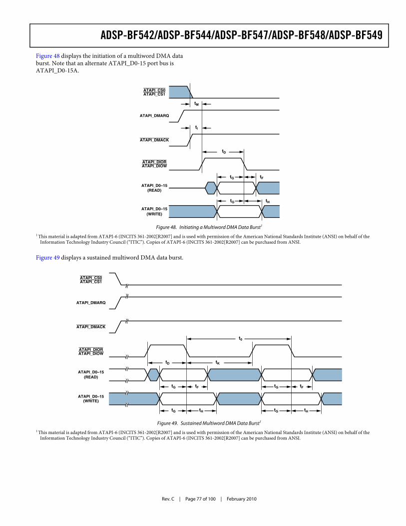
ADSP-BF542/ADSP-BF544/ADSP-BF547/ADSP-BF548/ADSP-BF549
Rev. C | Page 77 of 100 | February 2010
Figure 48 displays the initiation of a multiword DMA data burst. Note that an alternate ATAPI_D0-15 port bus is ATAPI_D0-15A.
Figure 49 displays a sustained multiword DMA data burst.
Figure 48. Initiating a Multiword DMA Data Burst1
1 This material is adapted from ATAPI-6 (INCITS 361-2002[R2007] and is used with permission of the American National Standards Institute (ANSI) on behalf of the Information Technology Industry Council (“ITIC”). Copies of ATAPI-6 (INCITS 361-2002[R2007] can be purchased from ANSI.
tM
tI
tD
tG tF
tG tH
ATAPI_DMARQ
ATAPI_CS0ATAPI_CS1
ATAPI_DMACK
ATAPI_DIORATAPI_DIOW
ATAPI_D0–15(READ)
ATAPI_D0–15(WRITE)
Figure 49. Sustained Multiword DMA Data Burst1
1 This material is adapted from ATAPI-6 (INCITS 361-2002[R2007] and is used with permission of the American National Standards Institute (ANSI) on behalf of the Information Technology Industry Council (“ITIC”). Copies of ATAPI-6 (INCITS 361-2002[R2007] can be purchased from ANSI.
ATAPI_DMARQ
ATAPI_D0–15
ATAPI_D0–15
ATAPI_CS0ATAPI_CS1
ATAPI_DIORATAPI_DIOW
t0
tD
tG tF
tG tH tG tH
tG tF
tK
(READ)
(WRITE)
ATAPI_DMACK
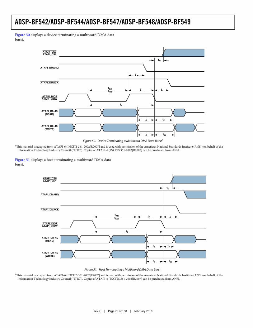
Rev. C | Page 78 of 100 | February 2010
ADSP-BF542/ADSP-BF544/ADSP-BF547/ADSP-BF548/ADSP-BF549
Figure 50 displays a device terminating a multiword DMA data burst.
Figure 51 displays a host terminating a multiword DMA data burst.
Figure 50. Device Terminating a Multiword DMA Data Burst1
1 This material is adapted from ATAPI-6 (INCITS 361-2002[R2007] and is used with permission of the American National Standards Institute (ANSI) on behalf of the Information Technology Industry Council (“ITIC”). Copies of ATAPI-6 (INCITS 361-2002[R2007] can be purchased from ANSI.
ATAPI_DMARQ
ATAPI_D0–15
ATAPI_D0–15
ATAPI_CS0ATAPI_CS1
ATAPI_DMACK
ATAPI_DIORATAPI_DIOW
tN
t0
tD tJ
tG tF
tLR
tG tH
tKRtKW
(READ)
(WRITE)
Figure 51. Host Terminating a Multiword DMA Data Burst1
1 This material is adapted from ATAPI-6 (INCITS 361-2002[R2007] and is used with permission of the American National Standards Institute (ANSI) on behalf of the Information Technology Industry Council (“ITIC”). Copies of ATAPI-6 (INCITS 361-2002[R2007] can be purchased from ANSI.
ATAPI_DMARQ
ATAPI_D0–15
ATAPI_D0–15
ATAPI_CS0ATAPI_CS1
ATAPI_DMACK
ATAPI_DIORATAPI_DIOW
t0
tN
tKRtKW
tD tJ
tG tF
tG tH
(READ)
(WRITE)
ADSP-BF542/ADSP-BF544/ADSP-BF547/ADSP-BF548/ADSP-BF549
Rev. C | Page 79 of 100 | February 2010
ATAPI Ultra DMA Data-In Transfer Timing Table 60 and Figure 52 through Figure 55 describe the ATAPI ultra DMA data-in data transfer timing.
Table 60. ATAPI Ultra DMA Data-In Transfer Timing
ATAPI ParameterATAPI_ULTRA_TIM_x Timing Register Setting1 Timing Equation
tDS Data setup time at host N/A TSK3 + tSUDU
tDH Data hold time at host N/A TSK3 + tHDU
tCVS CRC word valid setup time at host TDVS TDVS × tSCLK – (tSK1 + tSK2)tCVH CRC word valid hold time at host TACK TACK × tSCLK – (tSK1 + tSK2)tLI Limited interlock time N/A 2 × tBD + 2 × tSCLK + tOD
tMLI Interlock time with minimum TZAH, TCVS (TZAH + TCVS) × tSCLK – (4 × tBD + 4 × tSCLK + 2 × tOD)tAZ Maximum time allowed for output drivers to
releaseN/A 0
tZAH Minimum delay time required for output TZAH 2 × tSCLK + TZAH × tSCLK + tSCLK
tENV2 ATAPI_DMACK to ATAPI_DIOR/DIOW TENV (TENV × tSCLK) +/- (tSK1 + tSK2)
tRP ATAPI_DMACK to ATAPI_DIOR/DIOW TRP TRP × tSCLK – (tSK1 + tSK2 + tSK4) tACK Setup and hold times for ATAPI_DMACK TACK TACK × tSCLK – (tSK1 + tSK2)
1 ATAPI Timing Register Setting should be programmed with a value that guarantees parameter compliance with the ATA ANSI specification for ATA device mode of operation.2 This timing equation can be used to calculate both the minimum and maximum tENV.
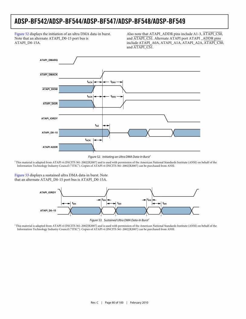
Rev. C | Page 80 of 100 | February 2010
ADSP-BF542/ADSP-BF544/ADSP-BF547/ADSP-BF548/ADSP-BF549
Figure 52 displays the initiation of an ultra DMA data-in burst. Note that an alternate ATAPI_D0-15 port bus is ATAPI_D0-15A.
Also note that ATAPI_ADDR pins include A1-3, ATAPI_CS0, and ATAPI_CS1. Alternate ATAPI port ATAPI _ADDR pins include ATAPI_A0A, ATAPI_A1A, ATAPI_A2A, ATAPI_CS0, and ATAPI_CS1.
Figure 53 displays a sustained ultra DMA data-in burst. Note that an alternate ATAPI_D0-15 port bus is ATAPI_D0-15A.
Figure 52. Initiating an Ultra DMA Data-In Burst1
1 This material is adapted from ATAPI-6 (INCITS 361-2002[R2007] and is used with permission of the American National Standards Institute (ANSI) on behalf of the Information Technology Industry Council (“ITIC”). Copies of ATAPI-6 (INCITS 361-2002[R2007] can be purchased from ANSI.
ATAPI_DMARQ
ATAPI_IORDY
ATAPI_D0–15
ATAPI ADDR
tENVtACK
tENVtACK
tAZ
tACK
ATAPI_DMACK
ATAPI_DIOW
ATAPI_DIOR
Figure 53. Sustained Ultra DMA Data-In Burst1
1 This material is adapted from ATAPI-6 (INCITS 361-2002[R2007] and is used with permission of the American National Standards Institute (ANSI) on behalf of the Information Technology Industry Council (“ITIC”). Copies of ATAPI-6 (INCITS 361-2002[R2007] can be purchased from ANSI.
ATAPI_IORDY
ATAPI_D0–15
tDH tDH
tDStDH
tDS
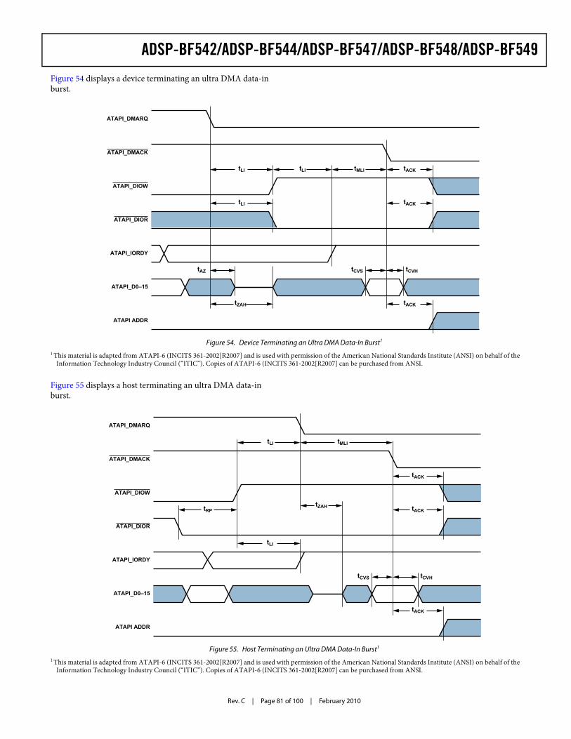
ADSP-BF542/ADSP-BF544/ADSP-BF547/ADSP-BF548/ADSP-BF549
Rev. C | Page 81 of 100 | February 2010
Figure 54 displays a device terminating an ultra DMA data-in burst.
Figure 55 displays a host terminating an ultra DMA data-in burst.
Figure 54. Device Terminating an Ultra DMA Data-In Burst1
1 This material is adapted from ATAPI-6 (INCITS 361-2002[R2007] and is used with permission of the American National Standards Institute (ANSI) on behalf of the Information Technology Industry Council (“ITIC”). Copies of ATAPI-6 (INCITS 361-2002[R2007] can be purchased from ANSI.
ATAPI_DMARQ
ATAPI_IORDY
ATAPI_D0–15
ATAPI ADDR
ATAPI_DMACK
ATAPI_DIOW
ATAPI_DIOR
tMLI tACK
tACK
tLItLI
tLI
tZAH
tAZ tCVS tCVH
tACK
Figure 55. Host Terminating an Ultra DMA Data-In Burst1
1 This material is adapted from ATAPI-6 (INCITS 361-2002[R2007] and is used with permission of the American National Standards Institute (ANSI) on behalf of the Information Technology Industry Council (“ITIC”). Copies of ATAPI-6 (INCITS 361-2002[R2007] can be purchased from ANSI.
ATAPI_DMARQ
ATAPI_IORDY
ATAPI_D0–15
ATAPI ADDR
ATAPI_DMACK
ATAPI_DIOW
ATAPI_DIOR
tLI tMLI
tZAHtRP
tACK
tACK
tACK
tLI
tCVS tCVH
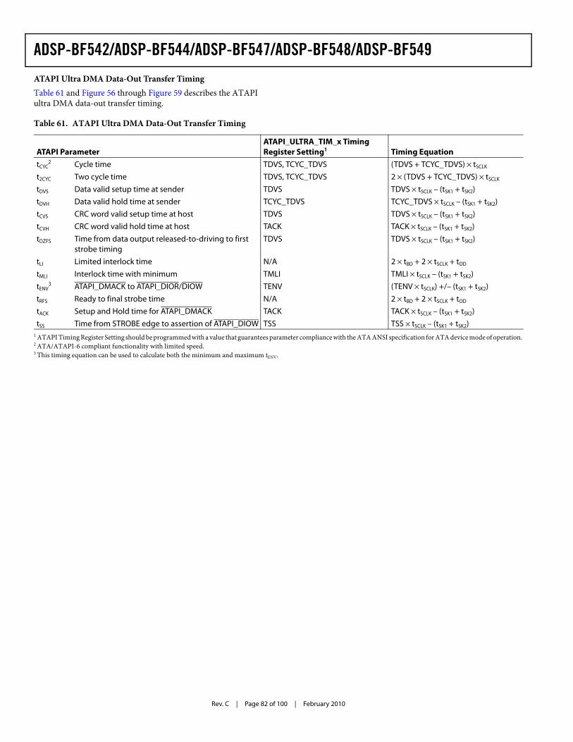
Rev. C | Page 82 of 100 | February 2010
ADSP-BF542/ADSP-BF544/ADSP-BF547/ADSP-BF548/ADSP-BF549
ATAPI Ultra DMA Data-Out Transfer Timing Table 61 and Figure 56 through Figure 59 describes the ATAPI ultra DMA data-out transfer timing.
Table 61. ATAPI Ultra DMA Data-Out Transfer Timing
ATAPI ParameterATAPI_ULTRA_TIM_x Timing Register Setting1 Timing Equation
tCYC2 Cycle time TDVS, TCYC_TDVS (TDVS + TCYC_TDVS) × tSCLK
t2CYC Two cycle time TDVS, TCYC_TDVS 2 × (TDVS + TCYC_TDVS) × tSCLK
tDVS Data valid setup time at sender TDVS TDVS × tSCLK – (tSK1 + tSK2)tDVH Data valid hold time at sender TCYC_TDVS TCYC_TDVS × tSCLK – (tSK1 + tSK2)tCVS CRC word valid setup time at host TDVS TDVS × tSCLK – (tSK1 + tSK2)tCVH CRC word valid hold time at host TACK TACK × tSCLK – (tSK1 + tSK2)tDZFS Time from data output released-to-driving to first
strobe timingTDVS TDVS × tSCLK – (tSK1 + tSK2)
tLI Limited interlock time N/A 2 × tBD + 2 × tSCLK + tOD
tMLI Interlock time with minimum TMLI TMLI × tSCLK – (tSK1 + tSK2)tENV
3 ATAPI_DMACK to ATAPI_DIOR/DIOW TENV (TENV × tSCLK) +/– (tSK1 + tSK2)tRFS Ready to final strobe time N/A 2 × tBD + 2 × tSCLK + tOD
tACK Setup and Hold time for ATAPI_DMACK TACK TACK × tSCLK – (tSK1 + tSK2)tSS Time from STROBE edge to assertion of ATAPI_DIOW TSS TSS × tSCLK – (tSK1 + tSK2)
1 ATAPI Timing Register Setting should be programmed with a value that guarantees parameter compliance with the ATA ANSI specification for ATA device mode of operation. 2 ATA/ATAPI-6 compliant functionality with limited speed.3 This timing equation can be used to calculate both the minimum and maximum tENV.
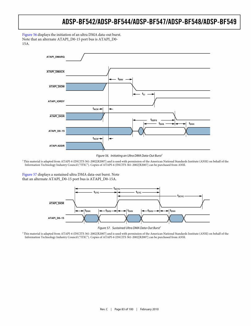
ADSP-BF542/ADSP-BF544/ADSP-BF547/ADSP-BF548/ADSP-BF549
Rev. C | Page 83 of 100 | February 2010
Figure 56 displays the initiation of an ultra DMA data-out burst. Note that an alternate ATAPI_D0-15 port bus is ATAPI_D0-15A.
Figure 57 displays a sustained ultra DMA data-out burst. Note that an alternate ATAPI_D0-15 port bus is ATAPI_D0-15A.
Figure 56. Initiating an Ultra DMA Data-Out Burst1
1 This material is adapted from ATAPI-6 (INCITS 361-2002[R2007] and is used with permission of the American National Standards Institute (ANSI) on behalf of the Information Technology Industry Council (“ITIC”). Copies of ATAPI-6 (INCITS 361-2002[R2007] can be purchased from ANSI.
ATAPI_DMARQ
ATAPI_IORDY
ATAPI ADDR
ATAPI_D0–15
tENV
tACK
tACK
ATAPI_DMACK
ATAPI_DIOW
ATAPI_DIOR
tLI
tDVS tDVH
tDZFS
Figure 57. Sustained Ultra DMA Data-Out Burst1
1 This material is adapted from ATAPI-6 (INCITS 361-2002[R2007] and is used with permission of the American National Standards Institute (ANSI) on behalf of the Information Technology Industry Council (“ITIC”). Copies of ATAPI-6 (INCITS 361-2002[R2007] can be purchased from ANSI.
ATAPI_D0–15
ATAPI_DIOR
t2CYCtCYC
tDVH tDVH tDVHtDVStDVS
tCYCt2CYC
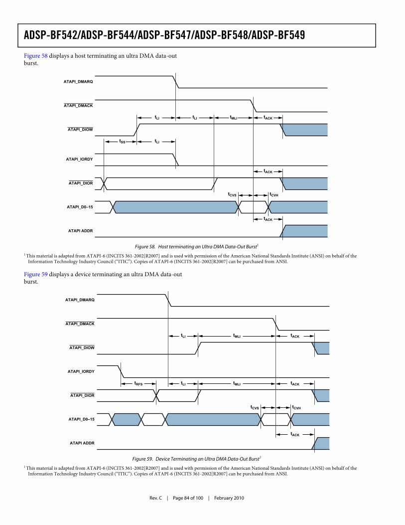
Rev. C | Page 84 of 100 | February 2010
ADSP-BF542/ADSP-BF544/ADSP-BF547/ADSP-BF548/ADSP-BF549
Figure 58 displays a host terminating an ultra DMA data-out burst.
Figure 59 displays a device terminating an ultra DMA data-out burst.
Figure 58. Host terminating an Ultra DMA Data-Out Burst1
1 This material is adapted from ATAPI-6 (INCITS 361-2002[R2007] and is used with permission of the American National Standards Institute (ANSI) on behalf of the Information Technology Industry Council (“ITIC”). Copies of ATAPI-6 (INCITS 361-2002[R2007] can be purchased from ANSI.
ATAPI_DMARQ
ATAPI_IORDY
ATAPI ADDR
ATAPI_D0–15
ATAPI_DMACK
ATAPI_DIOW
ATAPI_DIOR
tLI
tLItSS
tMLItLI tACK
tACK
tACK
tCVS tCVH
Figure 59. Device Terminating an Ultra DMA Data-Out Burst1
1 This material is adapted from ATAPI-6 (INCITS 361-2002[R2007] and is used with permission of the American National Standards Institute (ANSI) on behalf of the Information Technology Industry Council (“ITIC”). Copies of ATAPI-6 (INCITS 361-2002[R2007] can be purchased from ANSI.
ATAPI_DMARQ
ATAPI_IORDY
ATAPI ADDR
ATAPI_D0–15
ATAPI_DMACK
ATAPI_DIOW
ATAPI_DIOR
tLI tACKtMLI
tRFS
tCVS tCVH
tACK
tLI tACKtMLI
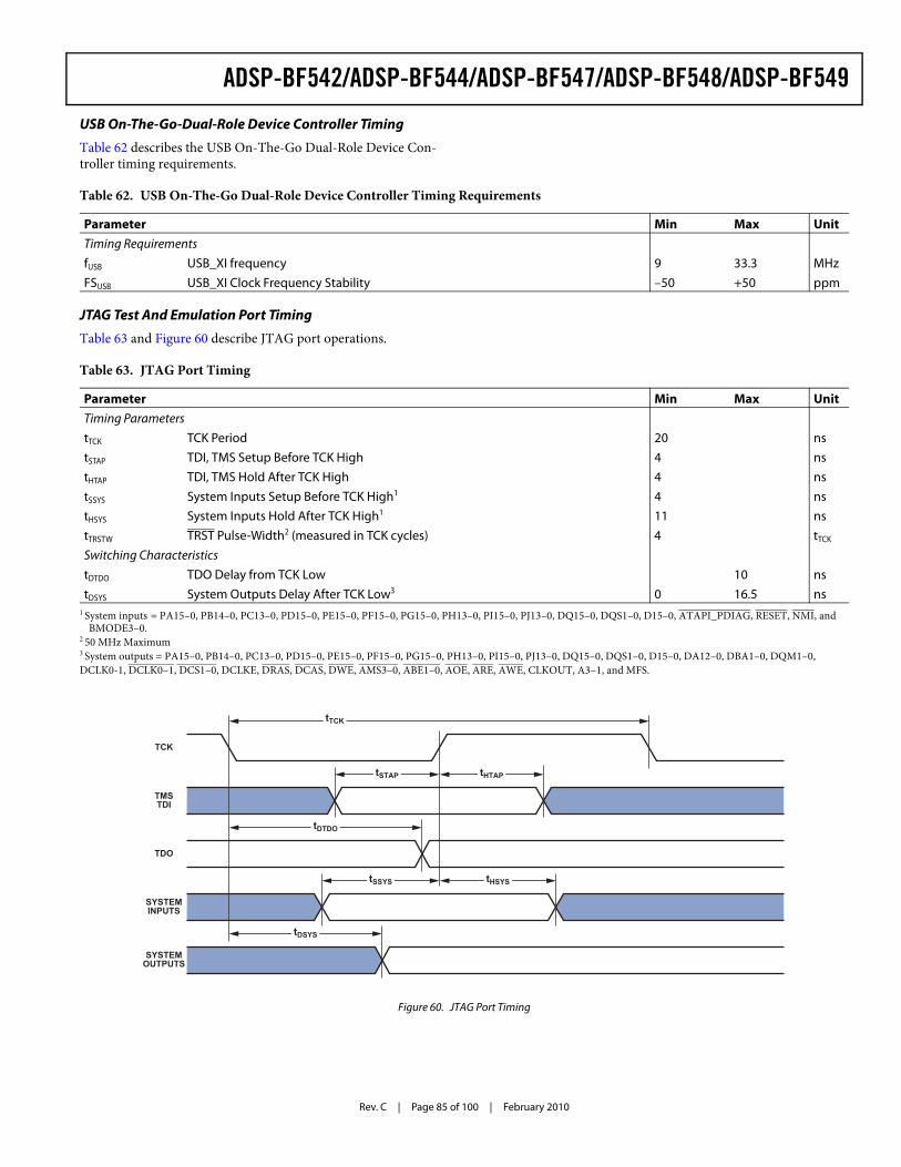
ADSP-BF542/ADSP-BF544/ADSP-BF547/ADSP-BF548/ADSP-BF549
Rev. C | Page 85 of 100 | February 2010
USB On-The-Go-Dual-Role Device Controller Timing
Table 62 describes the USB On-The-Go Dual-Role Device Con-troller timing requirements.
JTAG Test And Emulation Port Timing
Table 63 and Figure 60 describe JTAG port operations.
Table 62. USB On-The-Go Dual-Role Device Controller Timing Requirements
Parameter Min Max UnitTiming RequirementsfUSB USB_XI frequency 9 33.3 MHzFSUSB USB_XI Clock Frequency Stability –50 +50 ppm
Table 63. JTAG Port Timing
Parameter Min Max UnitTiming ParameterstTCK TCK Period 20 nstSTAP TDI, TMS Setup Before TCK High 4 nstHTAP TDI, TMS Hold After TCK High 4 nstSSYS System Inputs Setup Before TCK High1 4 nstHSYS System Inputs Hold After TCK High1 11 nstTRSTW TRST Pulse-Width2 (measured in TCK cycles) 4 tTCK
Switching CharacteristicstDTDO TDO Delay from TCK Low 10 nstDSYS System Outputs Delay After TCK Low3 0 16.5 ns
1 System inputs = PA15–0, PB14–0, PC13–0, PD15–0, PE15–0, PF15–0, PG15–0, PH13–0, PI15–0, PJ13–0, DQ15–0, DQS1–0, D15–0, ATAPI_PDIAG, RESET, NMI, and BMODE3–0.
2 50 MHz Maximum3 System outputs = PA15–0, PB14–0, PC13–0, PD15–0, PE15–0, PF15–0, PG15–0, PH13–0, PI15–0, PJ13–0, DQ15–0, DQS1–0, D15–0, DA12–0, DBA1–0, DQM1–0, DCLK0-1, DCLK0–1, DCS1–0, DCLKE, DRAS, DCAS, DWE, AMS3–0, ABE1–0, AOE, ARE, AWE, CLKOUT, A3–1, and MFS.
Figure 60. JTAG Port Timing
TCK
TMSTDI
TDO
SYSTEMINPUTS
SYSTEMOUTPUTS
tTCK
tSTAP tHTAP
tDTDO
tSSYS tHSYS
tDSYS
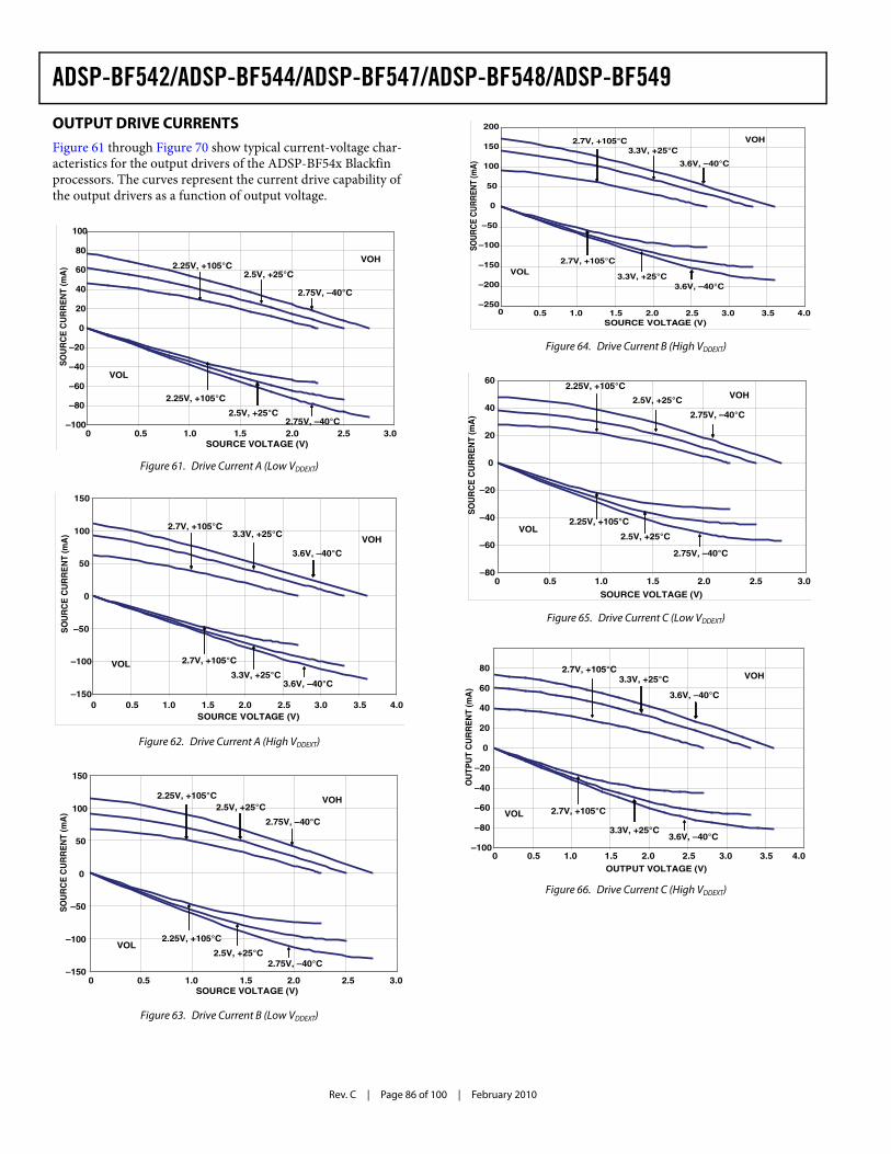
Rev. C | Page 86 of 100 | February 2010
ADSP-BF542/ADSP-BF544/ADSP-BF547/ADSP-BF548/ADSP-BF549
OUTPUT DRIVE CURRENTSFigure 61 through Figure 70 show typical current-voltage char-acteristics for the output drivers of the ADSP-BF54x Blackfin processors. The curves represent the current drive capability of the output drivers as a function of output voltage.
Figure 61. Drive Current A (Low VDDEXT)
Figure 62. Drive Current A (High VDDEXT)
Figure 63. Drive Current B (Low VDDEXT)
–100
–80
–60
–40
–20
0
20
40
60
80
100
0 0.5 1.0 1.5 2.0 2.5 3.0SOURCE VOLTAGE (V)
SO
UR
CE
CU
RR
EN
T(m
A)
VOL
VOH2.25V, +105°C
2.5V, +25°C
2.75V, –40°C
2.25V, +105°C
2.5V, +25°C2.75V, –40°C
–150
–100
–50
0
50
100
150
0 0.5 1.0 1.5 2.0 2.5 3.0 3.5 4.0SOURCE VOLTAGE (V)
SO
UR
CE
CU
RR
EN
T(m
A) VOH
VOL
2.7V, +105°C3.3V, +25°C
3.6V, –40°C
2.7V, +105°C
3.3V, +25°C3.6V, –40°C
–150
–100
–50
0
50
100
150
0 0.5 1.0 1.5 2.0 2.5 3.0SOURCE VOLTAGE (V)
SO
UR
CE
CU
RR
EN
T(m
A)
VOH
VOL
2.25V, +105°C2.5V, +25°C
2.75V, –40°C
2.25V, +105°C
2.5V, +25°C2.75V, –40°C
Figure 64. Drive Current B (High VDDEXT)
Figure 65. Drive Current C (Low VDDEXT)
Figure 66. Drive Current C (High VDDEXT)
–250
–200
–150
–100
–50
0
50
100
150
200
0 0.5 1.0 1.5 2.0 2.5 3.0 3.5 4.0SOURCE VOLTAGE (V)
SOU
RC
EC
UR
REN
T(m
A)
VOH
VOL
2.7V, +105°C3.3V, +25°C
3.6V, –40°C
2.7V, +105°C
3.3V, +25°C3.6V, –40°C
–80
–60
–40
–20
0
20
40
60
0 0.5 1.0 1.5 2.0 2.5 3.0
SOURCE VOLTAGE (V)
SO
UR
CE
CU
RR
EN
T(m
A)
VOH
VOL
2.25V, +105°C
2.5V, +25°C
2.75V, –40°C
2.25V, +105°C
2.5V, +25°C
2.75V, –40°C
–100
–80
–60
–40
–20
0
20
40
60
80
0 0.5 1.0 1.5 2.0 2.5 3.0 3.5 4.0OUTPUT VOLTAGE (V)
OU
TPU
TC
UR
RE
NT
(mA
)
VOH
VOL
2.7V, +105°C3.3V, +25°C
3.6V, –40°C
2.7V, +105°C
3.3V, +25°C3.6V, –40°C
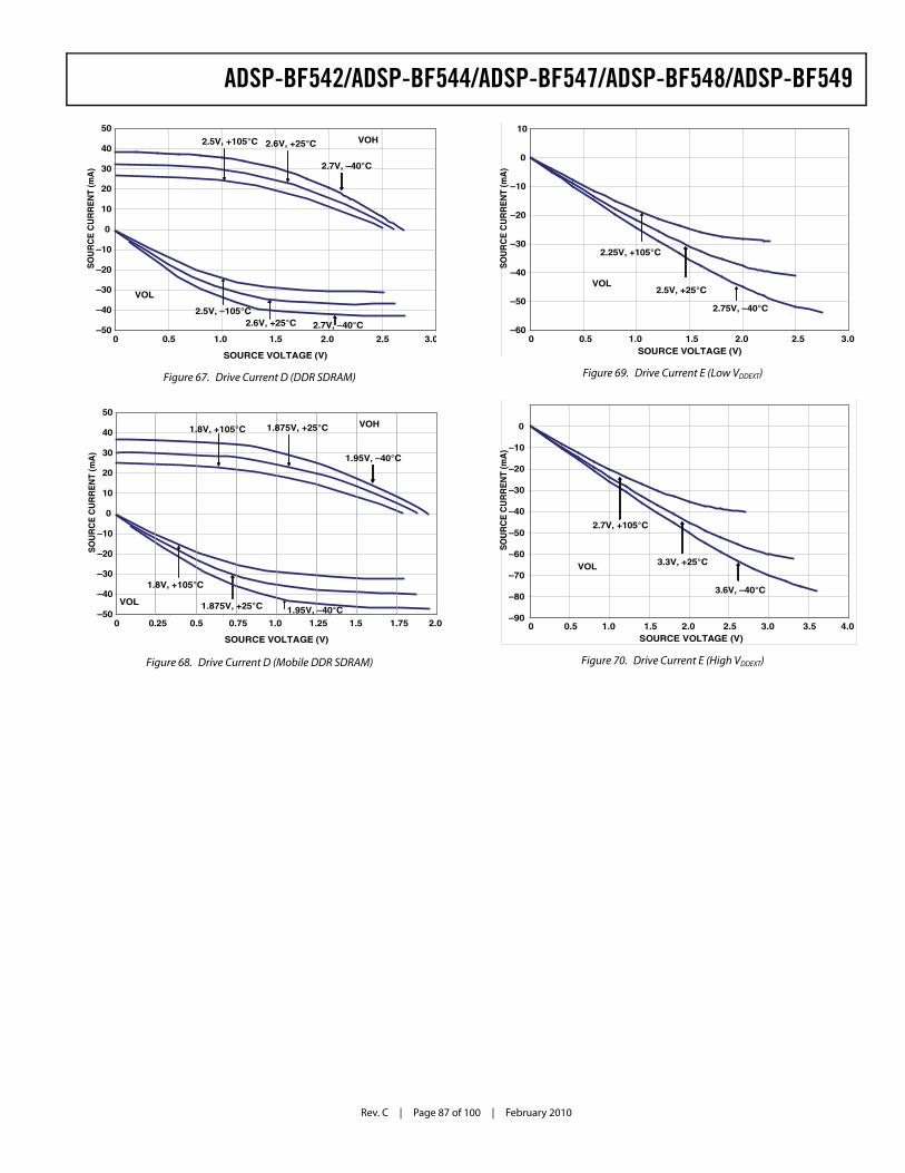
ADSP-BF542/ADSP-BF544/ADSP-BF547/ADSP-BF548/ADSP-BF549
Rev. C | Page 87 of 100 | February 2010
Figure 67. Drive Current D (DDR SDRAM)
Figure 68. Drive Current D (Mobile DDR SDRAM)
–50
–40
–30
–20
–10
0
10
20
30
40
50
0 0.5 1.0 1.5 2.0 2.5 3.0
SOURCE VOLTAGE (V)
SO
UR
CE
CU
RR
EN
T(m
A)
VOH
VOL
2.6V, +25°C
2.7V, –40°C
2.6V, +25°C 2.7V, –40°C
2.5V, +105°C
2.5V, –105°C
–50
–40
–30
–20
–10
0
10
20
30
40
50
0 0.25 0.5 0.75 1.0 1.25 2.0
SOURCE VOLTAGE (V)
SO
UR
CE
CU
RR
EN
T(m
A)
VOH
VOL
1.875V, +25°C
1.95V, –40°C
1.875V, +25°C 1.95V, –40°C
1.8V, +105°C
1.8V, +105°C
1.5 1.75
Figure 69. Drive Current E (Low VDDEXT)
Figure 70. Drive Current E (High VDDEXT)
–60
–50
–40
–30
–20
–10
0
10
0 0.5 1.0 1.5 2.0 2.5 3.0SOURCE VOLTAGE (V)
SO
UR
CE
CU
RR
EN
T(m
A)
VOL
2.25V, +105°C
2.5V, +25°C
2.75V, –40°C
–90
–80
–70
–60
–50
–40
–30
–20
–10
0
0 0.5 1.0 1.5 2.0 2.5 3.0 3.5 4.0SOURCE VOLTAGE (V)
SO
UR
CE
CU
RR
EN
T(m
A)
VOL
2.7V, +105°C
3.3V, +25°C
3.6V, –40°C
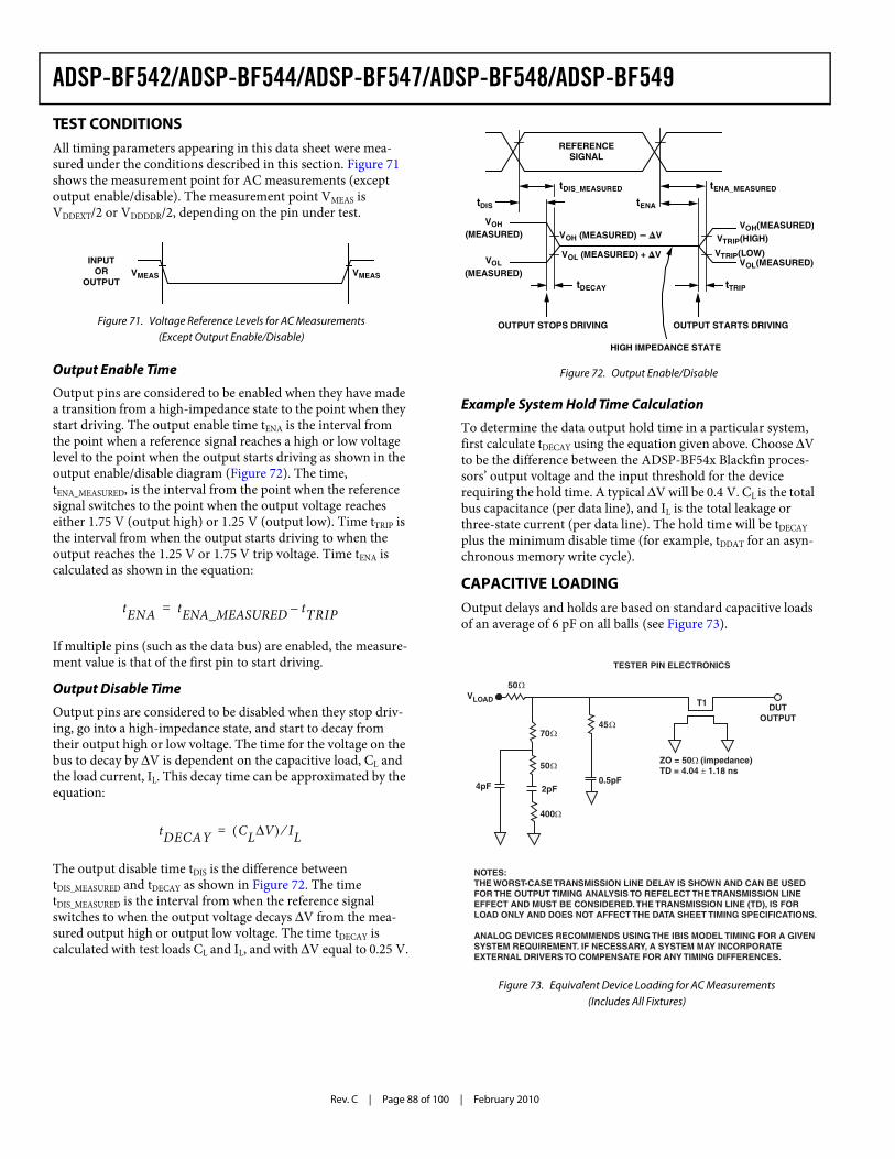
Rev. C | Page 88 of 100 | February 2010
ADSP-BF542/ADSP-BF544/ADSP-BF547/ADSP-BF548/ADSP-BF549
TEST CONDITIONSAll timing parameters appearing in this data sheet were mea-sured under the conditions described in this section. Figure 71 shows the measurement point for AC measurements (except output enable/disable). The measurement point VMEAS is VDDEXT/2 or VDDDDR/2, depending on the pin under test.
Output Enable Time
Output pins are considered to be enabled when they have made a transition from a high-impedance state to the point when they start driving. The output enable time tENA is the interval from the point when a reference signal reaches a high or low voltage level to the point when the output starts driving as shown in the output enable/disable diagram (Figure 72). The time, tENA_MEASURED, is the interval from the point when the reference signal switches to the point when the output voltage reaches either 1.75 V (output high) or 1.25 V (output low). Time tTRIP is the interval from when the output starts driving to when the output reaches the 1.25 V or 1.75 V trip voltage. Time tENA is calculated as shown in the equation:
If multiple pins (such as the data bus) are enabled, the measure-ment value is that of the first pin to start driving.
Output Disable Time
Output pins are considered to be disabled when they stop driv-ing, go into a high-impedance state, and start to decay from their output high or low voltage. The time for the voltage on the bus to decay by ∆V is dependent on the capacitive load, CL and the load current, IL. This decay time can be approximated by the equation:
The output disable time tDIS is the difference between tDIS_MEASURED and tDECAY as shown in Figure 72. The time tDIS_MEASURED is the interval from when the reference signal switches to when the output voltage decays ∆V from the mea-sured output high or output low voltage. The time tDECAY is calculated with test loads CL and IL, and with ∆V equal to 0.25 V.
Example System Hold Time Calculation
To determine the data output hold time in a particular system, first calculate tDECAY using the equation given above. Choose ∆V to be the difference between the ADSP-BF54x Blackfin proces-sors’ output voltage and the input threshold for the device requiring the hold time. A typical ∆V will be 0.4 V. CL is the total bus capacitance (per data line), and IL is the total leakage or three-state current (per data line). The hold time will be tDECAY plus the minimum disable time (for example, tDDAT for an asyn-chronous memory write cycle).
CAPACITIVE LOADINGOutput delays and holds are based on standard capacitive loads of an average of 6 pF on all balls (see Figure 73).
Figure 71. Voltage Reference Levels for AC Measurements (Except Output Enable/Disable)
INPUTOR
OUTPUTVMEAS VMEAS
tENA tENA_MEASURED tTRIP–=
tDECAY CL V∆( ) IL⁄=
Figure 72. Output Enable/Disable
Figure 73. Equivalent Device Loading for AC Measurements (Includes All Fixtures)
REFERENCESIGNAL
tDIS
OUTPUT STARTS DRIVING
VOH (MEASURED) V
VOL (MEASURED) + V
tDIS_MEASURED
VOH(MEASURED)
VOL(MEASURED)
VTRIP(HIGH)VOH(MEASURED)
VOL(MEASURED)
HIGH IMPEDANCE STATE
OUTPUT STOPS DRIVING
tENA
tDECAY
tENA_MEASURED
tTRIP
VTRIP(LOW)
T1
ZO = 50 (impedance)TD = 4.04 1.18 ns
2pF
TESTER PIN ELECTRONICS
50
0.5pF
70
400
45
4pF
NOTES:THE WORST-CASE TRANSMISSION LINE DELAY IS SHOWN AND CAN BE USEDFOR THE OUTPUT TIMING ANALYSIS TO REFELECT THE TRANSMISSION LINEEFFECT AND MUST BE CONSIDERED. THE TRANSMISSION LINE (TD), IS FOR LOAD ONLY AND DOES NOT AFFECT THE DATA SHEET TIMING SPECIFICATIONS.
ANALOG DEVICES RECOMMENDS USING THE IBIS MODEL TIMING FOR A GIVEN SYSTEM REQUIREMENT. IF NECESSARY, A SYSTEM MAY INCORPORATE EXTERNAL DRIVERS TO COMPENSATE FOR ANY TIMING DIFFERENCES.
VLOADDUT
OUTPUT
50
ADSP-BF542/ADSP-BF544/ADSP-BF547/ADSP-BF548/ADSP-BF549
Rev. C | Page 89 of 100 | February 2010
VLOAD is equal to VDDEXT/2 or VDDDDR/2, depending on the pin under test. Figure 74 through Figure 85 on Page 91 show how output rise time varies with capacitance. The delay and hold specifications given should be derated by a factor derived from these figures. The graphs in these figures may not be linear out-side the ranges shown.
TYPICAL RISE AND FALL TIMES
Figure 74. Typical Rise and Fall Times (10% to 90%) vs. Load Capacitance for Driver A at VDDEXT = 2.25 V
Figure 75. Typical Rise and Fall Times (10% to 90%) vs. Load Capacitance for Driver A at VDDEXT = 3.65 V
LOAD CAPACITANCE (pF)
RISE TIME
RIS
E A
ND
FA
LL
TIM
E n
s (1
0% t
o 9
0%)
14
12
10
8
6
4
2
00 50 100 150 200 250
FALL TIME
LOAD CAPACITANCE (pF)
RISE TIME
RIS
E A
ND
FA
LL
TIM
E n
s (1
0% t
o 9
0%)
12
10
8
6
4
2
00 50 100 150 200 250
FALL TIME
Figure 76. Typical Rise and Fall Times (10% to 90%) vs. Load Capacitance for Driver B at VDDEXT = 2.25 V
Figure 77. Typical Rise and Fall Times (10% to 90%) vs. Load Capacitance for Driver B at VDDEXT = 3.65 V
LOAD CAPACITANCE (pF)
RISE TIME
RIS
E A
ND
FA
LL
TIM
E n
s (1
0% t
o 9
0%)
12
10
8
6
4
2
00 50 100 150 200 250
FALL TIME
LOAD CAPACITANCE (pF)
RISE TIME
RIS
E A
ND
FA
LL
TIM
E n
s (1
0% t
o 9
0%)
10
9
8
7
6
5
4
3
2
1
00 50 100 150 200 250
FALL TIME
Rev. C | Page 90 of 100 | February 2010
ADSP-BF542/ADSP-BF544/ADSP-BF547/ADSP-BF548/ADSP-BF549
Figure 78. Typical Rise and Fall Times (10% to 90%) vs. Load Capacitance for Driver C at VDDEXT = 2.25 V
Figure 79. Typical Rise and Fall Times (10% to 90%) vs. Load Capacitance for Driver C at VDDEXT = 3.65 V
Figure 80. Typical Rise and Fall Times (10% to 90%) vs. Load Capacitance for Driver D DDR SDRAM at VDDDDR= 2.5V
LOAD CAPACITANCE (pF)
RISE TIME
RIS
E A
ND
FA
LL
TIM
E n
s (1
0% t
o 9
0%)
25
30
20
15
10
5
00 50 100 150 200 250
FALL TIME
LOAD CAPACITANCE (pF)
RISE TIME
RIS
E A
ND
FA
LL
TIM
E n
s (1
0% t
o 9
0%)
20
18
16
14
12
10
8
6
4
2
00 50 100 150 200 250
FALL TIME
LOAD CAPACITANCE (pF)
RISE/FALL TIME
RIS
E A
ND
FA
LL
TIM
E n
s (1
0% t
o 9
0%)
5
6
4
3
2
1
00 10 20 30 40 50 60 70
Figure 81. Typical Rise and Fall Times (10% to 90%) vs. Load Capacitance for Driver D DDR SDRAM at VDDDDR= 2.7V
Figure 82. Typical Rise and Fall Times (10% to 90%) vs. Load Capacitance for Driver D Mobile DDR SDRAM at VDDDDR = 1.8V
Figure 83. Typical Rise and Fall Times (10% to 90%) vs. Load Capacitance for Driver D Mobile DDR SDRAM at VDDDDR = 1.95V
LOAD CAPACITANCE (pF)
RISE/FALL TIME
RIS
E A
ND
FA
LL
TIM
E n
s (1
0% t
o 9
0%)
5
6
4
3
2
1
00 10 20 30 40 7050 60
LOAD CAPACITANCE (pF)
RISE/FALL TIME
RIS
E A
ND
FA
LL
TIM
E n
s (1
0% t
o 9
0%)
2.5
3
2
1.5
1
.5
00 10 20 30 40 50 60 70
3.5
4
LOAD CAPACITANCE (pF)
RISE/FALL TIME
RIS
E A
ND
FA
LL
TIM
E n
s (1
0% t
o 9
0%)
2.5
3
2
1.5
1
.5
00 10 20 30 40 50 60 70
3.5
4
ADSP-BF542/ADSP-BF544/ADSP-BF547/ADSP-BF548/ADSP-BF549
Rev. C | Page 91 of 100 | February 2010
THERMAL CHARACTERISTICSTo determine the junction temperature on the application printed circuit board use
where:TJ =junction temperature (C)TCASE = case temperature (C) measured by customer at top cen-ter of package.ΨJT = from Table 71PD = power dissipation. (See Table 18 on Page 38 for a method to calculate PD.)Values of θJA are provided for package comparison and printed circuit board design considerations. θJA can be used for a first order approximation of TJ by the equation
where:TA = ambient temperature (C)Table 64 lists values for θJC and θJB parameters. These values are provided for package comparison and printed circuit board design considerations. Airflow measurements in Table 64 com-ply with JEDEC standards JESD51-2 and JESD51-6, and the junction-to-board measurement complies with JESD51-8. The junction-to-case measurement complies with MIL-STD-883 (Method 1012.1). All measurements use a 2S2P JEDEC testboard.
Figure 84. Typical Fall Time (10% to 90%) vs. Load Capacitance for Driver E at VDDEXT = 2.7 V
Figure 85. Typical Fall Time (10% to 90%) vs. Load Capacitance for Driver E at VDDEXT = 3.65 V
LOAD CAPACITANCE (pF)
FAL
L T
IME
ns
(10%
to
90%
)
132
128
124
120
116
1080 50 100 150 200 250
FALL TIME
112
LOAD CAPACITANCE (pF)
FAL
LT
IME
ns
(10%
to
90%
)
124
120
116
112
108
1000 50 100 150 200 250
FALL TIME
104
Table 64. Thermal Characteristics, 400-Ball CSP_BGA
Parameter Condition Typical UnitθJA 0 linear m/s air flow 18.4 C/W
1 linear m/s air flow 15.8 C/W2 linear m/s air flow 15.0 C/W
θJB 9.75 C/WθJC 6.37 C/WΨJT 0 linear m/s air flow 0.27 C/W
1 linear m/s air flow 0.60 C/W2 linear m/s air flow 0.66 C/W
TJ TCASE ΨJT PD×( )+=
TJ TA θJA PD×( )+=
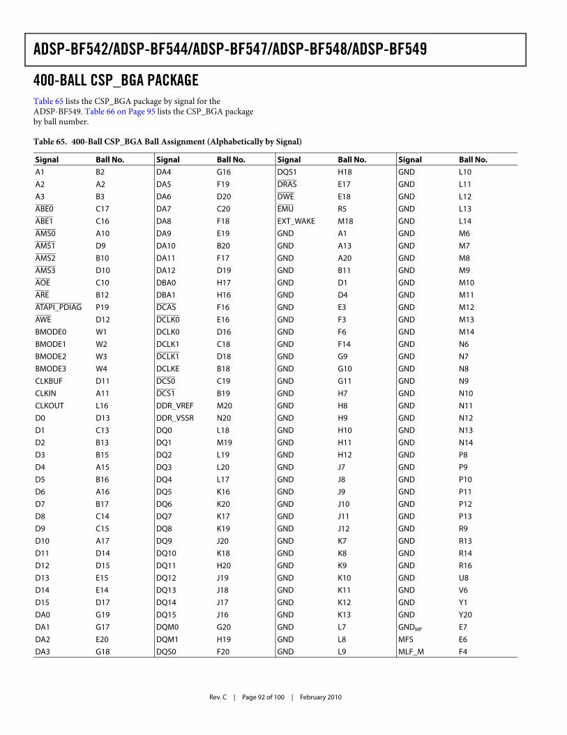
Rev. C | Page 92 of 100 | February 2010
ADSP-BF542/ADSP-BF544/ADSP-BF547/ADSP-BF548/ADSP-BF549
400-BALL CSP_BGA PACKAGETable 65 lists the CSP_BGA package by signal for the ADSP-BF549. Table 66 on Page 95 lists the CSP_BGA package by ball number.
Table 65. 400-Ball CSP_BGA Ball Assignment (Alphabetically by Signal)
Signal Ball No. Signal Ball No. Signal Ball No. Signal Ball No.A1 B2 DA4 G16 DQS1 H18 GND L10A2 A2 DA5 F19 DRAS E17 GND L11A3 B3 DA6 D20 DWE E18 GND L12ABE0 C17 DA7 C20 EMU R5 GND L13ABE1 C16 DA8 F18 EXT_WAKE M18 GND L14AMS0 A10 DA9 E19 GND A1 GND M6AMS1 D9 DA10 B20 GND A13 GND M7AMS2 B10 DA11 F17 GND A20 GND M8AMS3 D10 DA12 D19 GND B11 GND M9AOE C10 DBA0 H17 GND D1 GND M10ARE B12 DBA1 H16 GND D4 GND M11ATAPI_PDIAG P19 DCAS F16 GND E3 GND M12AWE D12 DCLK0 E16 GND F3 GND M13BMODE0 W1 DCLK0 D16 GND F6 GND M14BMODE1 W2 DCLK1 C18 GND F14 GND N6BMODE2 W3 DCLK1 D18 GND G9 GND N7BMODE3 W4 DCLKE B18 GND G10 GND N8CLKBUF D11 DCS0 C19 GND G11 GND N9CLKIN A11 DCS1 B19 GND H7 GND N10CLKOUT L16 DDR_VREF M20 GND H8 GND N11D0 D13 DDR_VSSR N20 GND H9 GND N12D1 C13 DQ0 L18 GND H10 GND N13D2 B13 DQ1 M19 GND H11 GND N14D3 B15 DQ2 L19 GND H12 GND P8D4 A15 DQ3 L20 GND J7 GND P9D5 B16 DQ4 L17 GND J8 GND P10D6 A16 DQ5 K16 GND J9 GND P11D7 B17 DQ6 K20 GND J10 GND P12D8 C14 DQ7 K17 GND J11 GND P13D9 C15 DQ8 K19 GND J12 GND R9D10 A17 DQ9 J20 GND K7 GND R13D11 D14 DQ10 K18 GND K8 GND R14D12 D15 DQ11 H20 GND K9 GND R16D13 E15 DQ12 J19 GND K10 GND U8D14 E14 DQ13 J18 GND K11 GND V6D15 D17 DQ14 J17 GND K12 GND Y1DA0 G19 DQ15 J16 GND K13 GND Y20DA1 G17 DQM0 G20 GND L7 GNDMP E7DA2 E20 DQM1 H19 GND L8 MFS E6DA3 G18 DQS0 F20 GND L9 MLF_M F4
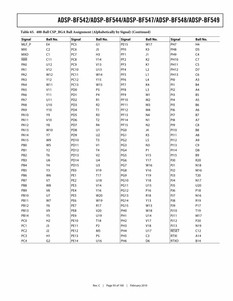
ADSP-BF542/ADSP-BF544/ADSP-BF547/ADSP-BF548/ADSP-BF549
Rev. C | Page 93 of 100 | February 2010
MLF_P E4 PC5 G1 PE15 W17 PH7 H4MXI C2 PC6 J5 PF0 K3 PH8 D5MXO C1 PC7 H3 PF1 J1 PH9 C4NMI C11 PC8 Y14 PF2 K2 PH10 C7PA0 U12 PC9 V13 PF3 K1 PH11 C5PA1 V12 PC10 U13 PF4 L2 PH12 D7PA2 W12 PC11 W14 PF5 L1 PH13 C6PA3 Y12 PC12 Y15 PF6 L4 PI0 A3PA4 W11 PC13 W15 PF7 K4 PI1 B4PA5 V11 PD0 P3 PF8 L3 PI2 A4PA6 Y11 PD1 P4 PF9 M1 PI3 B5PA7 U11 PD2 R1 PF10 M2 PI4 A5PA8 U10 PD3 R2 PF11 M3 PI5 B6PA9 Y10 PD4 T1 PF12 M4 PI6 A6PA10 Y9 PD5 R3 PF13 N4 PI7 B7PA11 V10 PD6 T2 PF14 N1 PI8 A7PA12 Y8 PD7 R4 PF15 N2 PI9 C8PA13 W10 PD8 U1 PG0 J4 PI10 B8PA14 Y7 PD9 U2 PG1 K5 PI11 A8PA15 W9 PD10 T3 PG2 L5 PI12 A9PB0 W5 PD11 V1 PG3 N3 PI13 C9PB1 Y2 PD12 T4 PG4 P1 PI14 D8PB2 T6 PD13 V2 PG5 V15 PI15 B9PB3 U6 PD14 U4 PG6 Y17 PJ0 R20PB4 Y4 PD15 U3 PG7 W16 PJ1 N18PB5 Y3 PE0 V19 PG8 V16 PJ2 M16PB6 W6 PE1 T17 PG9 Y19 PJ3 T20PB7 V7 PE2 U18 PG10 Y18 PJ4 N17PB8 W8 PE3 V14 PG11 U15 PJ5 U20PB9 V8 PE4 Y16 PG12 P16 PJ6 P18PB10 U7 PE5 W20 PG13 R18 PJ7 N16PB11 W7 PE6 W19 PG14 Y13 PJ8 R19PB12 Y6 PE7 R17 PG15 W13 PJ9 P17PB13 V9 PE8 V20 PH0 W18 PJ10 T19PB14 Y5 PE9 U19 PH1 U14 PJ11 M17PC0 H2 PE10 T18 PH2 V17 PJ12 P20PC1 J3 PE11 P2 PH3 V18 PJ13 N19PC2 J2 PE12 M5 PH4 U17 RESET C12PC3 H1 PE13 P5 PH5 C3 RTXI A14PC4 G2 PE14 U16 PH6 D6 RTXO B14
Table 65. 400-Ball CSP_BGA Ball Assignment (Alphabetically by Signal) (Continued)
Signal Ball No. Signal Ball No. Signal Ball No. Signal Ball No.
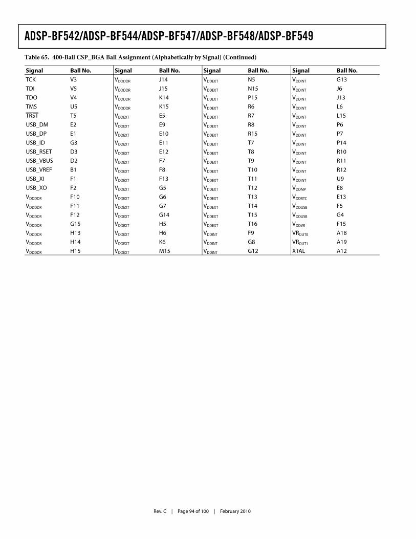
Rev. C | Page 94 of 100 | February 2010
ADSP-BF542/ADSP-BF544/ADSP-BF547/ADSP-BF548/ADSP-BF549
TCK V3 VDDDDR J14 VDDEXT N5 VDDINT G13TDI V5 VDDDDR J15 VDDEXT N15 VDDINT J6TDO V4 VDDDDR K14 VDDEXT P15 VDDINT J13TMS U5 VDDDDR K15 VDDEXT R6 VDDINT L6TRST T5 VDDEXT E5 VDDEXT R7 VDDINT L15USB_DM E2 VDDEXT E9 VDDEXT R8 VDDINT P6USB_DP E1 VDDEXT E10 VDDEXT R15 VDDINT P7USB_ID G3 VDDEXT E11 VDDEXT T7 VDDINT P14USB_RSET D3 VDDEXT E12 VDDEXT T8 VDDINT R10USB_VBUS D2 VDDEXT F7 VDDEXT T9 VDDINT R11USB_VREF B1 VDDEXT F8 VDDEXT T10 VDDINT R12USB_XI F1 VDDEXT F13 VDDEXT T11 VDDINT U9USB_XO F2 VDDEXT G5 VDDEXT T12 VDDMP E8VDDDDR F10 VDDEXT G6 VDDEXT T13 VDDRTC E13VDDDDR F11 VDDEXT G7 VDDEXT T14 VDDUSB F5VDDDDR F12 VDDEXT G14 VDDEXT T15 VDDUSB G4VDDDDR G15 VDDEXT H5 VDDEXT T16 VDDVR F15VDDDDR H13 VDDEXT H6 VDDINT F9 VROUT0 A18VDDDDR H14 VDDEXT K6 VDDINT G8 VROUT1 A19VDDDDR H15 VDDEXT M15 VDDINT G12 XTAL A12
Table 65. 400-Ball CSP_BGA Ball Assignment (Alphabetically by Signal) (Continued)
Signal Ball No. Signal Ball No. Signal Ball No. Signal Ball No.
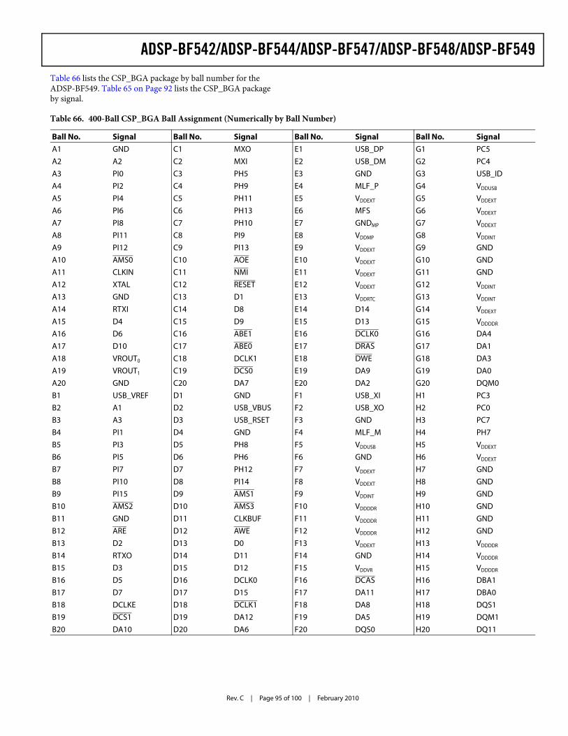
ADSP-BF542/ADSP-BF544/ADSP-BF547/ADSP-BF548/ADSP-BF549
Rev. C | Page 95 of 100 | February 2010
Table 66 lists the CSP_BGA package by ball number for the ADSP-BF549. Table 65 on Page 92 lists the CSP_BGA package by signal.
Table 66. 400-Ball CSP_BGA Ball Assignment (Numerically by Ball Number)
Ball No. Signal Ball No. Signal Ball No. Signal Ball No. SignalA1 GND C1 MXO E1 USB_DP G1 PC5A2 A2 C2 MXI E2 USB_DM G2 PC4A3 PI0 C3 PH5 E3 GND G3 USB_IDA4 PI2 C4 PH9 E4 MLF_P G4 VDDUSB
A5 PI4 C5 PH11 E5 VDDEXT G5 VDDEXT
A6 PI6 C6 PH13 E6 MFS G6 VDDEXT
A7 PI8 C7 PH10 E7 GNDMP G7 VDDEXT
A8 PI11 C8 PI9 E8 VDDMP G8 VDDINT
A9 PI12 C9 PI13 E9 VDDEXT G9 GNDA10 AMS0 C10 AOE E10 VDDEXT G10 GNDA11 CLKIN C11 NMI E11 VDDEXT G11 GNDA12 XTAL C12 RESET E12 VDDEXT G12 VDDINT
A13 GND C13 D1 E13 VDDRTC G13 VDDINT
A14 RTXI C14 D8 E14 D14 G14 VDDEXT
A15 D4 C15 D9 E15 D13 G15 VDDDDR
A16 D6 C16 ABE1 E16 DCLK0 G16 DA4A17 D10 C17 ABE0 E17 DRAS G17 DA1A18 VROUT0 C18 DCLK1 E18 DWE G18 DA3A19 VROUT1 C19 DCS0 E19 DA9 G19 DA0A20 GND C20 DA7 E20 DA2 G20 DQM0B1 USB_VREF D1 GND F1 USB_XI H1 PC3B2 A1 D2 USB_VBUS F2 USB_XO H2 PC0B3 A3 D3 USB_RSET F3 GND H3 PC7B4 PI1 D4 GND F4 MLF_M H4 PH7B5 PI3 D5 PH8 F5 VDDUSB H5 VDDEXT
B6 PI5 D6 PH6 F6 GND H6 VDDEXT
B7 PI7 D7 PH12 F7 VDDEXT H7 GNDB8 PI10 D8 PI14 F8 VDDEXT H8 GNDB9 PI15 D9 AMS1 F9 VDDINT H9 GNDB10 AMS2 D10 AMS3 F10 VDDDDR H10 GNDB11 GND D11 CLKBUF F11 VDDDDR H11 GNDB12 ARE D12 AWE F12 VDDDDR H12 GNDB13 D2 D13 D0 F13 VDDEXT H13 VDDDDR
B14 RTXO D14 D11 F14 GND H14 VDDDDR
B15 D3 D15 D12 F15 VDDVR H15 VDDDDR
B16 D5 D16 DCLK0 F16 DCAS H16 DBA1B17 D7 D17 D15 F17 DA11 H17 DBA0B18 DCLKE D18 DCLK1 F18 DA8 H18 DQS1B19 DCS1 D19 DA12 F19 DA5 H19 DQM1B20 DA10 D20 DA6 F20 DQS0 H20 DQ11
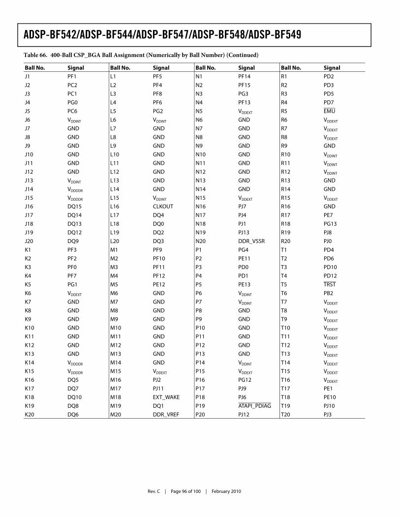
Rev. C | Page 96 of 100 | February 2010
ADSP-BF542/ADSP-BF544/ADSP-BF547/ADSP-BF548/ADSP-BF549
J1 PF1 L1 PF5 N1 PF14 R1 PD2J2 PC2 L2 PF4 N2 PF15 R2 PD3J3 PC1 L3 PF8 N3 PG3 R3 PD5J4 PG0 L4 PF6 N4 PF13 R4 PD7J5 PC6 L5 PG2 N5 VDDEXT R5 EMUJ6 VDDINT L6 VDDINT N6 GND R6 VDDEXT
J7 GND L7 GND N7 GND R7 VDDEXT
J8 GND L8 GND N8 GND R8 VDDEXT
J9 GND L9 GND N9 GND R9 GNDJ10 GND L10 GND N10 GND R10 VDDINT
J11 GND L11 GND N11 GND R11 VDDINT
J12 GND L12 GND N12 GND R12 VDDINT
J13 VDDINT L13 GND N13 GND R13 GNDJ14 VDDDDR L14 GND N14 GND R14 GNDJ15 VDDDDR L15 VDDINT N15 VDDEXT R15 VDDEXT
J16 DQ15 L16 CLKOUT N16 PJ7 R16 GNDJ17 DQ14 L17 DQ4 N17 PJ4 R17 PE7J18 DQ13 L18 DQ0 N18 PJ1 R18 PG13J19 DQ12 L19 DQ2 N19 PJ13 R19 PJ8J20 DQ9 L20 DQ3 N20 DDR_VSSR R20 PJ0K1 PF3 M1 PF9 P1 PG4 T1 PD4K2 PF2 M2 PF10 P2 PE11 T2 PD6K3 PF0 M3 PF11 P3 PD0 T3 PD10K4 PF7 M4 PF12 P4 PD1 T4 PD12K5 PG1 M5 PE12 P5 PE13 T5 TRSTK6 VDDEXT M6 GND P6 VDDINT T6 PB2K7 GND M7 GND P7 VDDINT T7 VDDEXT
K8 GND M8 GND P8 GND T8 VDDEXT
K9 GND M9 GND P9 GND T9 VDDEXT
K10 GND M10 GND P10 GND T10 VDDEXT
K11 GND M11 GND P11 GND T11 VDDEXT
K12 GND M12 GND P12 GND T12 VDDEXT
K13 GND M13 GND P13 GND T13 VDDEXT
K14 VDDDDR M14 GND P14 VDDINT T14 VDDEXT
K15 VDDDDR M15 VDDEXT P15 VDDEXT T15 VDDEXT
K16 DQ5 M16 PJ2 P16 PG12 T16 VDDEXT
K17 DQ7 M17 PJ11 P17 PJ9 T17 PE1K18 DQ10 M18 EXT_WAKE P18 PJ6 T18 PE10K19 DQ8 M19 DQ1 P19 ATAPI_PDIAG T19 PJ10K20 DQ6 M20 DDR_VREF P20 PJ12 T20 PJ3
Table 66. 400-Ball CSP_BGA Ball Assignment (Numerically by Ball Number) (Continued)
Ball No. Signal Ball No. Signal Ball No. Signal Ball No. Signal
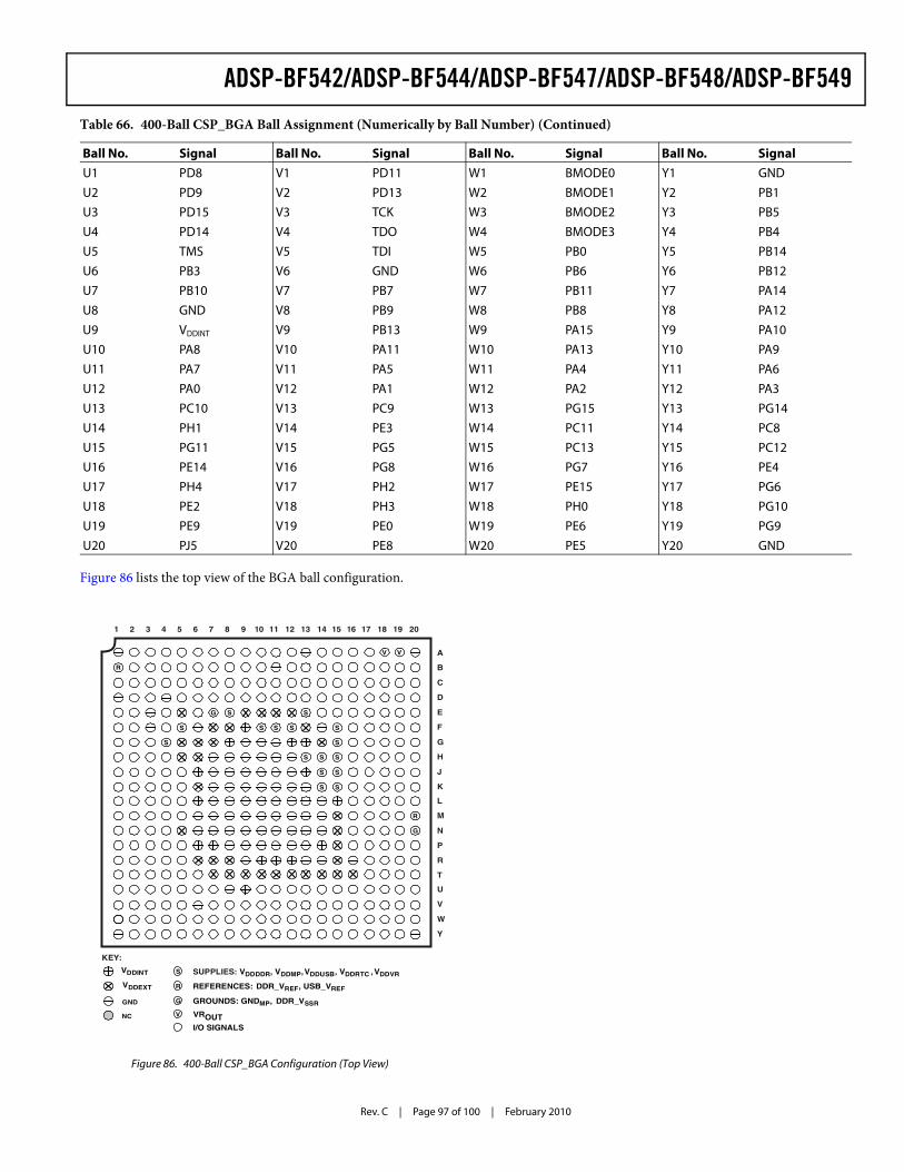
ADSP-BF542/ADSP-BF544/ADSP-BF547/ADSP-BF548/ADSP-BF549
Rev. C | Page 97 of 100 | February 2010
Figure 86 lists the top view of the BGA ball configuration.
U1 PD8 V1 PD11 W1 BMODE0 Y1 GNDU2 PD9 V2 PD13 W2 BMODE1 Y2 PB1U3 PD15 V3 TCK W3 BMODE2 Y3 PB5U4 PD14 V4 TDO W4 BMODE3 Y4 PB4U5 TMS V5 TDI W5 PB0 Y5 PB14U6 PB3 V6 GND W6 PB6 Y6 PB12U7 PB10 V7 PB7 W7 PB11 Y7 PA14U8 GND V8 PB9 W8 PB8 Y8 PA12U9 VDDINT V9 PB13 W9 PA15 Y9 PA10U10 PA8 V10 PA11 W10 PA13 Y10 PA9U11 PA7 V11 PA5 W11 PA4 Y11 PA6U12 PA0 V12 PA1 W12 PA2 Y12 PA3U13 PC10 V13 PC9 W13 PG15 Y13 PG14U14 PH1 V14 PE3 W14 PC11 Y14 PC8U15 PG11 V15 PG5 W15 PC13 Y15 PC12U16 PE14 V16 PG8 W16 PG7 Y16 PE4U17 PH4 V17 PH2 W17 PE15 Y17 PG6U18 PE2 V18 PH3 W18 PH0 Y18 PG10U19 PE9 V19 PE0 W19 PE6 Y19 PG9U20 PJ5 V20 PE8 W20 PE5 Y20 GND
Table 66. 400-Ball CSP_BGA Ball Assignment (Numerically by Ball Number) (Continued)
Ball No. Signal Ball No. Signal Ball No. Signal Ball No. Signal
Figure 86. 400-Ball CSP_BGA Configuration (Top View)
A
B
C
D
E
F
G
H
J
K
L
M
N
P
1 2 3 4 5 6 7 8 9 10 11 12 13 14 16 17 18 19 2015
VDDEXT
GND
VDDINT
I/O SIGNALS
KEY:
REFERENCES: DDR_VREF, USB_VREF
R
T
U
V
W
Y
NC
S
G
R
GROUNDS: GNDMP, DDR_VSSR
SUPPLIES: VDDDDR, VDDMP,VDDUSB, VDDRTC
V V
SG
R
S
G
R
S S
S S
S
S
S S
SS
S
S
S
VDDVR,
S
VROUTV
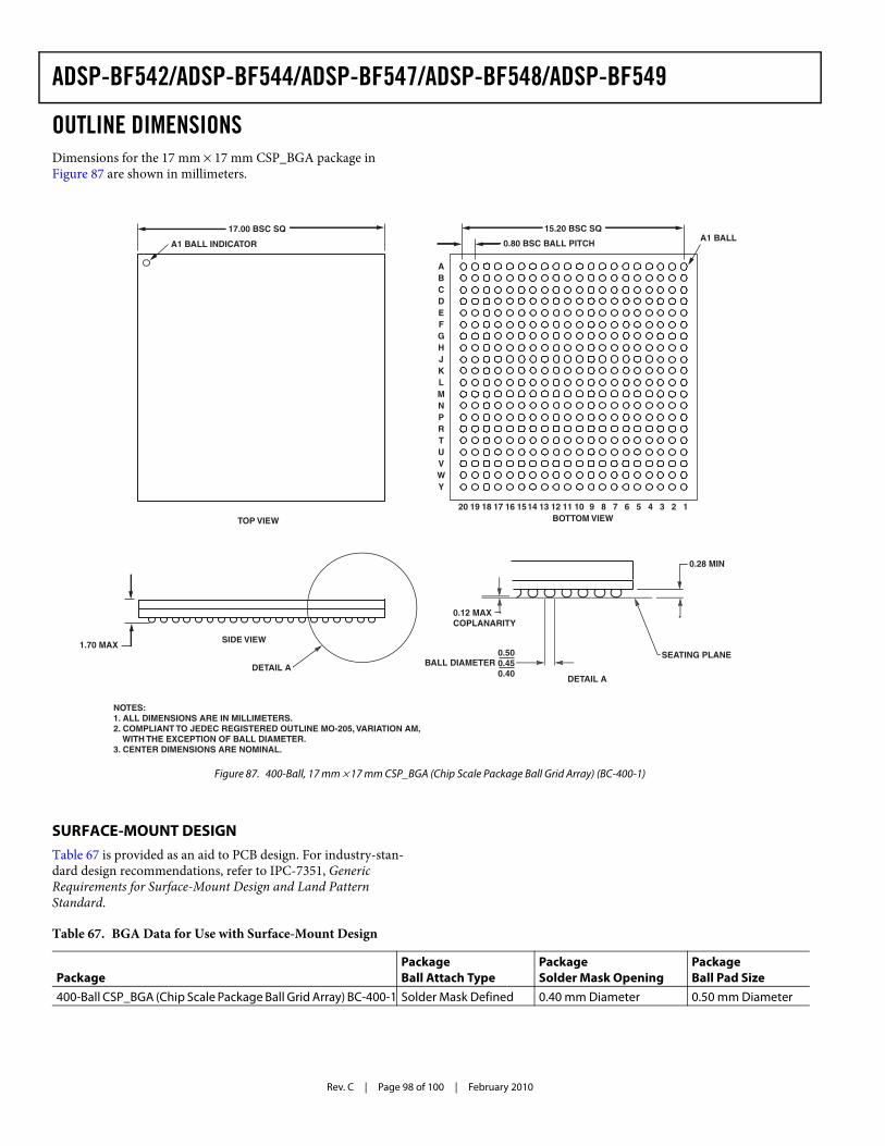
Rev. C | Page 98 of 100 | February 2010
ADSP-BF542/ADSP-BF544/ADSP-BF547/ADSP-BF548/ADSP-BF549
OUTLINE DIMENSIONSDimensions for the 17 mm × 17 mm CSP_BGA package in Figure 87 are shown in millimeters.
SURFACE-MOUNT DESIGNTable 67 is provided as an aid to PCB design. For industry-stan-dard design recommendations, refer to IPC-7351, Generic Requirements for Surface-Mount Design and Land Pattern Standard.
Figure 87. 400-Ball, 17 mm × 17 mm CSP_BGA (Chip Scale Package Ball Grid Array) (BC-400-1)
ABCDEFGHJKLMNPR
UVWY
T
BOTTOM VIEW20 19 18 17 1514 13 12 11 10 9 8 7 6 5 4 3 2 116
A1 BALL INDICATOR
NOTES:1. ALL DIMENSIONS ARE IN MILLIMETERS.2. COMPLIANT TO JEDEC REGISTERED OUTLINE MO-205, VARIATION AM, WITH THE EXCEPTION OF BALL DIAMETER.3. CENTER DIMENSIONS ARE NOMINAL.
SIDE VIEW
TOP VIEW
DETAIL A
17.00 BSC SQ 15.20 BSC SQ
0.80 BSC BALL PITCHA1 BALL
1.70 MAX
DETAIL A
SEATING PLANE0.500.450.40
BALL DIAMETER
0.12 MAXCOPLANARITY
0.28 MIN
Table 67. BGA Data for Use with Surface-Mount Design
PackagePackage Ball Attach Type
Package Solder Mask Opening
Package Ball Pad Size
400-Ball CSP_BGA (Chip Scale Package Ball Grid Array) BC-400-1 Solder Mask Defined 0.40 mm Diameter 0.50 mm Diameter
ADSP-BF542/ADSP-BF544/ADSP-BF547/ADSP-BF548/ADSP-BF549
Rev. C | Page 99 of 100 | February 2010
AUTOMOTIVE PRODUCTSSome ADSP-BF54x Blackfin processor models are available for automotive applications with controlled manufacturing. Note that these special models may have specifications that differ from the general release models.
The automotive grade products shown in Table 68 are available for use in automotive applications. Contact your local ADI account representative or authorized ADI product distributor for specific product ordering information. Note that all automo-tive products are RoHS compliant.
Table 68. Automotive Products
Product Family1 Temperature Range2 Speed Grade (Max) Package Description Package OptionADBF542WBBCZ-4xx –40°C to +85°C 400 MHz 400-Ball CSP_BGA BC-400-1ADBF542WBBCZ-5xx –40°C to +85°C 533 MHz 400-Ball CSP_BGA BC-400-1ADBF544WBBCZ-5xx –40°C to +85°C 533 MHz 400-Ball CSP_BGA BC-400-1ADBF549WBBCZ-5xx –40°C to +85°C 533 MHz 400-Ball CSP_BGA BC-400-1ADBF549MWBBCZ-5xx –40°C to +85°C 533 MHz 400-Ball CSP_BGA BC-400-1
1 The use of xx designates silicon revision2 Referenced temperature is ambient temperature.
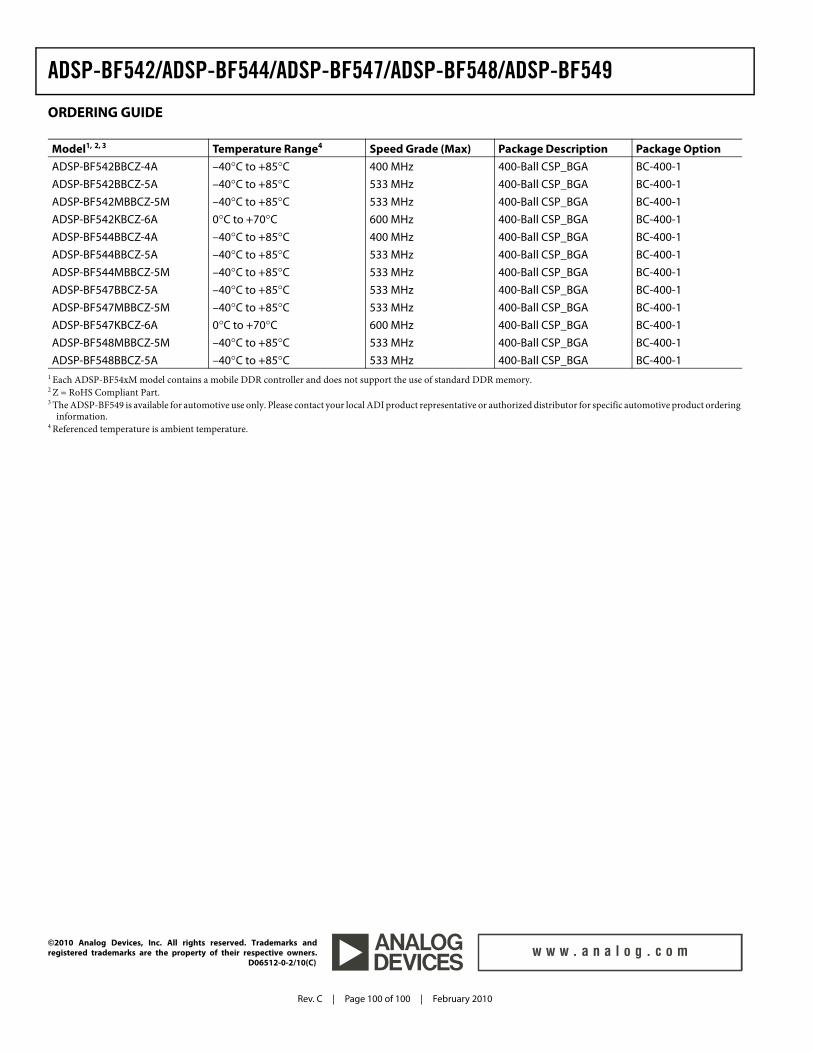
Rev. C | Page 100 of 100 | February 2010
ADSP-BF542/ADSP-BF544/ADSP-BF547/ADSP-BF548/ADSP-BF549
©2010 Analog Devices, Inc. All rights reserved. Trademarks andregistered trademarks are the property of their respective owners.
D06512-0-2/10(C)
ORDERING GUIDE
Model1, 2, 3
1 Each ADSP-BF54xM model contains a mobile DDR controller and does not support the use of standard DDR memory.2 Z = RoHS Compliant Part.3 The ADSP-BF549 is available for automotive use only. Please contact your local ADI product representative or authorized distributor for specific automotive product ordering
information.
Temperature Range4
4 Referenced temperature is ambient temperature.
Speed Grade (Max) Package Description Package OptionADSP-BF542BBCZ-4A –40°C to +85°C 400 MHz 400-Ball CSP_BGA BC-400-1ADSP-BF542BBCZ-5A –40°C to +85°C 533 MHz 400-Ball CSP_BGA BC-400-1ADSP-BF542MBBCZ-5M –40°C to +85°C 533 MHz 400-Ball CSP_BGA BC-400-1ADSP-BF542KBCZ-6A 0°C to +70°C 600 MHz 400-Ball CSP_BGA BC-400-1ADSP-BF544BBCZ-4A –40°C to +85°C 400 MHz 400-Ball CSP_BGA BC-400-1ADSP-BF544BBCZ-5A –40°C to +85°C 533 MHz 400-Ball CSP_BGA BC-400-1ADSP-BF544MBBCZ-5M –40°C to +85°C 533 MHz 400-Ball CSP_BGA BC-400-1ADSP-BF547BBCZ-5A –40°C to +85°C 533 MHz 400-Ball CSP_BGA BC-400-1ADSP-BF547MBBCZ-5M –40°C to +85°C 533 MHz 400-Ball CSP_BGA BC-400-1ADSP-BF547KBCZ-6A 0°C to +70°C 600 MHz 400-Ball CSP_BGA BC-400-1ADSP-BF548MBBCZ-5M –40°C to +85°C 533 MHz 400-Ball CSP_BGA BC-400-1ADSP-BF548BBCZ-5A –40°C to +85°C 533 MHz 400-Ball CSP_BGA BC-400-1