Embed Size (px)
Citation preview

BK3266 Datasheet v 0.5
© 2017 Beken Corporation Proprietary and Confidential Page 1 of 28
BK3266 Bluetooth Audio SoC Datasheet
Beken Corporation 41,1387 Zhangdong Rd, Shanghai 201203, China
PHONE: (86)21 5108 6811 FAX: (86)21 6087 1089
This document contains information that may be proprietary to, and/or secrets of, Beken Corporation. The
contents of this document should not be disclosed outside the companies without specific written permission.
Disclaimer: Descriptions of specific implementations are for illustrative purpose only, actual hardware implementation may differ.

Low Power Bluetooth Audio SoC v 0.5
© 2017 Beken Corporation Proprietary and Confidential Page 2 of 28
Revision History Rev. Date Remark 0.1 22/Sep/2017 Initial version 0.2 26/Sep/2017 Update pin list that line in will be no GPIO function 0.3 19/Oct/2017 Update TSSOP28 pin definition 0.4 20/Oct/2017 Typo correction
0.41 20/Oct/2017 Typo correction 0.5 11/Apr/2018 Add SOP16 package

BK3266 Datasheet v 0.5
© 2017 Beken Corporation Proprietary and Confidential Page 3 of 28
Contents
1. General Description ................................................................................................. 5
1.1. Features .......................................................................................................... 5 1.2. Applications ..................................................................................................... 5
2. Pin Definition ........................................................................................................... 6
3. Functional Description ........................................................................................... 12
3.1. Overview ........................................................................................................ 12 3.2. Modes of Operation ....................................................................................... 12 3.3. RF Transceiver .............................................................................................. 12 3.4. Bluetooth Baseband....................................................................................... 13 3.5. Audio Peripherals .......................................................................................... 13
3.5.1. 5 – Band Digital Equalizer ............................................................. 13 3.5.2. Stereo ADC and DAC .................................................................... 14 3.5.3. Microphone Input Amplifier and Bias ............................................. 14 3.5.4. Line-in Input ................................................................................... 14 3.5.5. Stereo Audio L/R Outputs .............................................................. 15
3.6. MCU .............................................................................................................. 15 3.7. FLASH Access Interface ................................................................................ 15 3.8. Beken Bluetooth Software Stack .................................................................... 15 3.9. Crystal Oscillator ............................................................................................ 15 3.10. Power Management ....................................................................................... 16 3.11. GPIO and LED Driver .................................................................................... 16 3.12. Timer and Watch Dog Timer .......................................................................... 17 3.13. PWM output ................................................................................................... 17 3.14. I2C and UART Interface ................................................................................. 18 3.15. SPI Interface .................................................................................................. 18 3.16. General Purpose SAR ADC ........................................................................... 18 3.17. SDIO Card Interface and USB interface ......................................................... 18 3.18. IrDA interface ................................................................................................. 19 3.19. I2S interface .................................................................................................. 19
4. Electrical Characteristics ....................................................................................... 20
4.1. Absolute Maximum Ratings ........................................................................... 20 4.2. Recommended Operating Conditions ............................................................ 20 4.3. System LDO .................................................................................................. 20 4.4. USB LDO ....................................................................................................... 20 4.5. BATTERY CHARGE ...................................................................................... 21 4.6. Analog LDO/BUCK ........................................................................................ 21 4.7. Digital LDO/BUCK ......................................................................................... 21 4.8. Crystal and Reference Clock ......................................................................... 21 4.9. Typical Power Consumption .......................................................................... 22 4.10. RF Characteristics ......................................................................................... 22 4.11. Audio Characteristics ..................................................................................... 22
5. About Qualification ................................................................................................ 23

Low Power Bluetooth Audio SoC v 0.5
© 2017 Beken Corporation Proprietary and Confidential Page 4 of 28
6. Package Information .............................................................................................. 24
6.1. QFN 4x4 32-pin package ............................................................................... 24 6.2. TSSOP28 package ........................................................................................ 25 6.3. QFN 5x5 40-pin package ............................................................................... 26 6.4. SOP16 package ............................................................................................. 27
7. Ordering Information .............................................................................................. 28

BK3266 Datasheet v 0.5
© 2017 Beken Corporation Proprietary and Confidential Page 5 of 28
1. General Description The BK3266 is a low power, highly integrated Bluetooth system on chip (SoC) audio device. It integrates a high performance Bluetooth RF transceiver, feature rich baseband processor, FLASH memory controller, multiple analog and digital peripherals, and a Bluetooth software stack including the audio, voice, and SPP profiles.
The cache based architecture enables full programmability with an SIP 8M FLASH memory device and can be used for both control and multimedia hybrid applications. The internal dual stereo ADC converts stereo analog input to digital signals that can be processed with a digital equalizer. Hardware realizations of the equalizer offload the MCU making the chip ideal for low power headset applications.
The device incorporates on-chip power management with linear and switch-mode buck regulators and also includes a 220 mA internal battery charge controller to further reduce external bill of material (BOM) costs.
1.1. Features Operation voltage from 2.8 V to 4.2 V
9 mA average current for A2DP
300 uA for 500 ms sniff current
0.8 uA deep sleep current
Bluetooth 4.2 classic and low energy
A2DP v1.3, AVRCP v1.6, HFP v1.7, HID v1.1, AVCTP v1.4, AVDTP v1.3, and SPP v1.2
True wireless stereo and two active link
Two wires UART download interface
16 bits stereo ADC and DAC
Stereo line in and dual microphone
Five bands digital hardware equalizer
SPI, UART, I2C, SDIO and USB
I2S master and slave interface with MCLK output
Interface for external PA and LNA
Up to 220 mA battery charge controller
1.2. Applications Bluetooth stereo speaker Bluetooth stereo headset Bluetooth control and multimedia hybrid
DCO
LDOs
POR
Charge
Audio DAC
Audio ADC 32 bit
MCU
Reset
DMA
EQ
ADCData RAM
FLASHI2S
M/S
SPI1
BIST
Bluetooth TransceiverDual Mode
3 Timers
Audio Digital Filter
USB
SD-Card
SPI2
Always on Domain
ROSC
RTC
Watch Dog
DPLL
D-Cache
I2C/UART
FIR/FFT
GPIO
Retention Regs
Temp. S
IrDA
6 PWMs
Figure 1. Block diagram of BK3266 Bluetooth Audio SoC
Low Power Bluetooth Audio SoC v 0.5
© 2017 Beken Corporation Proprietary and Confidential Page 6 of 28
2. Pin Definition The BK3266 is available in 16-pin SOP, 28-pin TSSOP package, 32-pin 4x4 mm2 QFN and 40-pin 5x5 mm2 QFN package.
9 10
11
12
13
14
15
16
RF
GPIO1_RXD
GPIO13_SD_DAT0
GPIO0_TXD
GPIO14 1
2
3
4
5
6
7
8
24
23
22
21
20
19
18
17
32
31
30
29
28
27
26
25
BK32664x4 QFN32
RSTN
GPI
O15
_GPI
O3
GPI
O11
_SD
_CLK
GPI
O12
_SD
_CM
D
VDD
DIG
SWD
SWA
VDD
ANA
VCC3SYS
VCC5USB
AUDRP
AUDRN
AUDLN
AUDLP
MIC
REF
MIC
RN
MIC
RP
GPI
O6_
USB
DP
VDD
BT
XOXI
VDDALON
LINER
LINEL
VCC
4BAT
GPI
O7_
USB
DN
VDDIO3VFLA
Figure 2 32-Pin QFN 4mmx4mm diagram
Table 1 Pin Description of 32-Pin Package
PIN
Name Description
1 GPIO14 GPIO14, JTAG_TDO/PWM5/ADC7/PCM_DOUT 2 GPIO13_SD_DA
T0 GPIO13, JTAG_TDI/PWM4/ADC6/PCM_DIN/SD_DATA0/SPI2_MISO
3 RSTN Reset pin, active low 4 RF RF port 5 GPIO0_TXD GPIO0, UART_TXD/I2C_SCL, Download port 6 GPIO1_RXD GPIO1, UART_RXD/I2C_SDA, Download port 7 LINER Line in L 8 LINEL Line in R

BK3266 Datasheet v 0.5
© 2017 Beken Corporation Proprietary and Confidential Page 7 of 28
9 GPIO15_GPIO3 GPIO15, also as GPIO3, SPI_SCK/ADC2/CLKOUT Soft shut down and wake up (active high)
10 GPIO11_SD_CLK
GPIO11, JTAG_TCK/PWM2/ADC4/PCM_SYNC/SD_CLK//SPI2_SCK
11 GPIO12_SD_CMD
GPIO12, JTAG_TMS/PWM3/PCM_CLK/SD_CMD/SPI2_MOSI
12 VDDDIG Digital LDO output 13 SWD Buck component 14 SWA Buck component 15 VDDANA Analog LDO output 16 VCC4BAT Battery input 17 VCC3SYS System LDO output 18 VCC5USB USB charge power input 19 VDDALON Always on power supply 20 VDDIO3VFLA FLASH power supply 21 AUDRP Audio right channel positive 22 AUDRN Audio right channel negative 23 AUDLN Audio left channel negative 24 AUDLP Audio left channel positive 25 MICREF Microphone reference voltage 26 MICRN Microphone input negative 27 MICRP Microphone input positive 28 GPIO7_USBDN GPIO7, PWM1 / USBN 29 GPIO6_USBDP GPIO6, PWM0 / USBP 30 VDDBT Bluetooth RF LDO output 31 XO Crystal output 32 XI Crystal input

Low Power Bluetooth Audio SoC v 0.5
© 2017 Beken Corporation Proprietary and Confidential Page 8 of 28
BK3266TSSOP28
MICRP
VDDIO3VFLA
USBDP_GPIO6
XI
XO
VDDBT
GND
GPIO3_ADC2
RF
GPIO2
GPIO1_RXD
AUDRP
USBDN_GPIO7 GPIO12_SD_CMD
GPIO11_SD_CLK
AUDLP
GPIO13_SD_DATA0
GPIO15
GPIO0_TXD
LINER
LINEL
VDDANA
VCC4BAT
VCOM
VCC3SYS
1
2
3
4
5
6
7
8
9
10
11
12
13
14
28
27
26
25
24
23
22
21
20
19
18
17
16
15 VDDDIG
VDDALON
MICRN
Figure 3 TSSOP28 Package
Table 2 Pin Description of 28-Pin Package
PIN
Name Description
1 GPIO7_USBDN GPIO7, PWM1 / USBN 2 GPIO6_USBDP GPIO6, PWM0 / USBP 3 VDDBT Bluetooth RF LDO output 4 XO Crystal output 5 XI Crystal input 6 GND Ground 7 RF RF port 8 GPIO0_TXD GPIO0, UART_TXD/I2C_SCL, Download port 9 GPIO1_RXD GPIO1, UART_RXD/I2C_SDA, Download port 10 LINER Line in L 11 LINEL Line in R 12 GPIO2 GPIO2, SPI_CSN/ADC1/IrDA/Capture Time 13 GPIO15 GPIO15, Soft shut down and wake up (active high) 14 GPIO3_ADC2 GPIO3, SPI_SCK/ADC2/CLKOUT 15 VDDDIG Digital LDO output 16 VDDANA Analog LDO output 17 VCC4BAT Battery input

BK3266 Datasheet v 0.5
© 2017 Beken Corporation Proprietary and Confidential Page 9 of 28
18 VCC3SYS System LDO output 19 VDDALON Always on power supply 20 VDDIO3VFLA FLASH power supply 21 MICRP Microphone input positive 22 AUDRP Audio right channel positive 23 AUDLP Audio left channel positive 24 VCOM Common mode decoupling capacitor 25 GPIO13_SD_DA
T0 GPIO13, JTAG_TDI/PWM4/ADC6/PCM_DIN/SD_DATA0/SPI2_MISO
26 MICRP Microphone input negative 27 GPIO11_SD_CL
K GPIO11, JTAG_TCK/PWM2/ADC4/PCM_SYNC/SD_CLK//SPI2_SCK
28 GPIO12_SD_CMD
GPIO12, JTAG_TMS/PWM3/PCM_CLK/SD_CMD/SPI2_MOSI
11
12
13
14
15
16
17
18
RF
GPIO1_RXD
GPIO13
GPIO0_TXD
GPIO14
1
2
3
4
5
6
7
8
30
29
28
27
26
25
24
23
40
39
38
37
36
35
34
33
BK32665x5 QFN40
Full Functional
GPIO10
GPIO9
GPI
O8
GPI
O15
GPI
O11
GPI
O12
VDD
DIG
SWD
SWA
VDD
ANA
VCC4BAT
VCC3SYS
VCC5USB
AUDRP
AUDRN
AUDLN
AUDLP
LIN
ER
USB
DN
USB
DP
VDD
BT
XOXI
9
10
19
20
21
22
31
32
GPIO4
GPIO5
GPI
O3
GN
D
MIC
REF
MIC
RN
MIC
RP
LIN
EL
GPIO2
VDDALON
VCOM
VDDIO3VFLA
Figure 4 40-Pin QFN 5mmx5mm diagram
Table 3 Pin Description of 40-Pin Package

Low Power Bluetooth Audio SoC v 0.5
© 2017 Beken Corporation Proprietary and Confidential Page 10 of 28
PIN
Name Description
1 GPIO2 GPIO2, SPI_CSN/ADC1/IrDA/Capture Time 2 GPIO14 GPIO14, JTAG_TDO/PWM5/ADC7/PCM_DOUT 3 GPIO13 GPIO13,
JTAG_TDI/PWM4/ADC6/PCM_DIN/SD_DATA0/SPI2_MISO
4 RF RF port 5 GPIO10 GPIO10, SD_DATA0/RX_EN/SPI2_MISO 6 GPIO0_TXD GPIO0, UART_TXD/I2C_SCL, Download port 7 GPIO1_RXD GPIO1, UART_RXD/I2C_SDA, Download port 8 GPIO9 GPIO9, SD_CMD/TX_EN/SPI2_MOSI 9 GPIO4 GPIO4, SPI_MOSI//I2C_SCL 10 GPIO5 GPIO5, SPI_MOSI//I2C_SCL 11 GPIO8 GPIO8, SD_CLK//SPI2_SCK 12 GPIO15 GPIO15, Soft shut down and wake up (active high) 13 GPIO3 GPIO3, SPI_SCK/ADC2/CLKOUT 14 GPIO11 GPIO11,
JTAG_TCK/PWM2/ADC4/PCM_SYNC/SD_CLK//SPI2_SCK
15 GPIO12 GPIO12, JTAG_TMS/PWM3/PCM_CLK/SD_CMD/SPI2_MOSI
16 VDDDIG Digital LDO output 17 SWD Buck component 18 GND Ground 19 SWA Buck component 20 VDDANA Analog LDO output 21 VCC4BAT Battery input 22 VCC3SYS System LDO output 23 VCC5USB USB charge power input 24 VDDALON Always on power supply 25 VDDIO3VFLA FLASH power supply 26 AUDRP Audio right channel positive 27 AUDRN Audio right channel negative 28 AUDLN Audio left channel negative 29 AUDLP Audio left channel positive 30 VCOM Common mode voltage for audio output 31 MICREF Microphone reference voltage 32 MICRN Microphone input negative 33 MICRP Microphone input positive 34 LINEL Line left channel input 35 LINER Line right channel input 36 USBDN GPIO7, PWM1 / USBN 37 USBDP GPIO6, PWM0 / USBP 38 VDDBT Bluetooth RF LDO output
BK3266 Datasheet v 0.5
© 2017 Beken Corporation Proprietary and Confidential Page 11 of 28
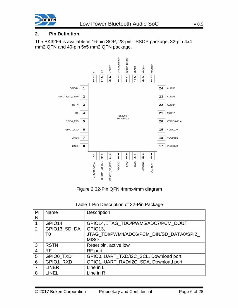
39 XO Crystal output 40 XI Crystal input
BK3266SO16B
SOP16
XI
XO
RF
GPIO1
GPIO0
VDDANA
VDDDIG
1
2
3
4
5
6
7
8
16
15
14
13
12
11
10
9GPIO15_GPIO3
MICRP
AUDLP
VCC3SYS
VCC4BAT
AUDRP
GPIO2
GND
MICRN
Figure 5 16-Pin SOP SO16B diagram
BK3266SO16A
SOP16
XI
XO
RF
GPIO1
GPIO0
VDDANAVDDDIG
1
2
3
4
5
6
7
8
16
15
14
13
12
11
10
9
GPIO15_GPIO3
MICRP
AUDLP
VCC3SYS
VCC4BAT
GND
MICRN
AUDRP
VCC5USB
Figure 6 16-Pin SOP SO16A diagram
There are two kinds of BK3266 SOP16 package, one for speaker and one for earpiece. Please refer to the pin description of other package types for SOP16 pin description.

Low Power Bluetooth Audio SoC v 0.5
© 2017 Beken Corporation Proprietary and Confidential Page 12 of 28
3. Functional Description
3.1. Overview
The BK3266 is a single-chip Bluetooth SoC offering advanced audio processing and low power consumption by utilizing dedicated hardware blocks such as a five band equalizer and a hardware accelerator to increase performance and offload the MCU. It has Bluetooth version 4.2 EDR stack and application profiles and can be used for both control and multimedia hybrid applications. The BK3266 includes a rich set of analog and digital peripherals that allow users to add features such as a microphone input, stereo line-in inputs, SDIO memory card, and an FM radio to a Bluetooth application enhancing overall user experience.
3.2. Modes of Operation
The general operation of the BK3266 is as follows. After system reset, the BK3266 enters the low power standby mode waiting for external circuitry via the GPIO interface to wake the device up. Once the device is awake, it will establish a connection with other Bluetooth devices using the Inquire and Paging states. After a connection is made the device can be placed into Active or Sniff mode depending on the master Bluetooth device Shutdown – In this mode all circuits are powered down except for the GPIO15 interface to allow external circuitry to wake-up the device. Software can enter this mode by write special register and system can only be waked up by active level applied on GPIO15. Standby – In this mode all circuits are powered down except the GPIO interface and a timer active to allow external circuitry and internal timer to wake-up the device. This is the default low power state of the chip while it is waiting to be used. There is no interaction with any Bluetooth devices in this state. Active – During this mode, the BK3266 and the other connected Bluetooth device are actively receiving and transmitting data on the channel. This data can be high fidelity audio, voice, or control commands depending on the application. Sniff – In this mode, the device remains active but listens and communicates at a reduced rate. The device maintains connection with the master with its Active Member Address (AM_ADDR) and goes to sleep and wakes up at assigned Sniff Intervals to exchange packets with the master. Test – The BK3266 provides a test mode to test the internal RAM memory BIST and other blocks. The test mode is normally not used.
3.3. RF Transceiver
The BK3266 integrates a high-performance Bluetooth transceiver and frequency synthesizer. The transceiver is fully differential and incorporates an integrated
BK3266 Datasheet v 0.5
© 2017 Beken Corporation Proprietary and Confidential Page 13 of 28
on-chip balun which transforms the single-ended RF signal from the antenna through pin, RFP_BT, into an internal differential balanced signal for the low noise amplifier (LNA). On the transmit side, the differential outputs of the power amplifier (PA) are combined and transformed to a single-ended output using the same on-chip balun thus enabling only one RF pin connection to the antenna for both transmit and receive operations. The device is able to output +8 dBm of transmit output power allowing users to develop a class 2 (+4 dBm) device with small printed circuit board (PCB) antenna. The frequency synthesizer is fully integrated and does not require any external components.
3.4. Bluetooth Baseband
The BK3266 Bluetooth baseband implements the Bluetooth version 4.2 Enhanced Data Rate (EDR) modem providing Basic Data Rate (BDR) 1 Mbps as well as the enhanced 2 Mbps, and 3 Mbps data rates.
Data Rate Modulation Bits/Symbol BDR: 1 Mbps GFSK 1
EDR: 2 Mbps π/4 DQPSK 2
EDR: 3 Mbps 8 DPSK 3
Table 4. BK3266 Bluetooth Modulation Formats The Bluetooth baseband utilizes a combination of both hardware blocks and firmware for the frequency hopping sequence generator, access code generation, detection, and correlation, encryption and decryption for security, forward error correction, 16-bit CRC, packet construction, and Bluetooth clocks and timers to optimize for power consumption and user programmability.
3.5. Audio Peripherals
The BK3266 comes with a rich set of audio peripherals to enhance the Bluetooth listening experience. The chip includes a 5-band digital equalizer, 96 dB signal-to-noise ratio (SNR) stereo analog-to-digital converter (ADC) and digital-to-analog converter (DAC), microphone input amplifier and bias, line-in input, and stereo audio left and right (L/R) outputs.
3.5.1. 5 – Band Digital Equalizer
A dedicated 5-band digital equalizer is implemented prior to digital-to-analog conversion to give users the option of customizing the frequency response of the audio output. The equalizer is implemented in hardware to reduce overall chip power consumption. The 5-band equalizer is easily configured using the BK3266

Low Power Bluetooth Audio SoC v 0.5
© 2017 Beken Corporation Proprietary and Confidential Page 14 of 28
software configuration tool kit. For more information, please refer to the BK3266 Software Configuration Tool Users Guide.
3.5.2. Stereo ADC and DAC
The BK3266 contains high fidelity 96 dB SNR stereo ADCs with sample rates of 8 kHz, 16 kHz, 44.1 kHz, or 48 kHz. The chip also integrates high fidelity 96 dB SNR stereo DACs with sample rates of 8 kHz, 16 kHz, 44.1 kHz or 48 kHz.
3.5.3. Microphone Input Amplifier and Bias
BK3266 contains a fully differential analog microphone input amplifier and a low-noise microphone bias generator. Expensive external components are not needed as the microphone amplifier and active bias circuitry are integrated into the chip allowing the microphone to be interfaced with only cheap passive resistors and capacitors. The microphone signal can be amplified with gain from -8 ~ 38dB with 0.5 dB step.
MIC
R32 k
C51uF
R42 k
C91uF
C61uF
MICRP MICRN MICREF
MIC
R43.9 k
C91uF
C61uF
MICRP MICREF
Differential Mode Single_End Mode Figure 7. Microphone Interface
3.5.4. Line-in Input
BK3266 includes stereo line-in inputs which connect to the stereo left and right channel ADCs through a 0~6 dB amplifier with 2 dB step. The digitized line-in inputs can be further processed with the 5-band equalizer prior to digital-to-analog conversion.

BK3266 Datasheet v 0.5
© 2017 Beken Corporation Proprietary and Confidential Page 15 of 28
3.5.5. Stereo Audio L/R Outputs
BK3266 provides high fidelity stereo audio L/R outputs capable of driving 16 Ω speakers with up to 30 pF of load capacitance.
3.6. MCU
The BK3266 includes a 32-bit internal RISC MCU, memory and a DMA bus controller to run the Bluetooth software stack and application while supporting efficient execution and data exchange with the internal SIP FLASH memory. The JTAG interface can be used for on-line debug and can also be configured as GPIO.
3.7. FLASH Access Interface
BK3266 internal RISC MCU operates with an external FLASH, which is used to store program code, external settings and configurations, and can also be used to store user data such as encryption key configuration and Bluetooth paring information.
3.8. Beken Bluetooth Software Stack
The BK3266 comes with Bluetooth version 4.2 + EDR compliant software stack which run on the internal 32-bit RISC MCU. The SoC also runs the application program removing the need for an external host controller. An external host can be connected through the UART interface for debugging purposes but is not needed to run the application. Beken Corporation provides a development kit that customers can use to configure their applications. The development kit includes a software configuration tool and reference software code for stereo-mode Bluetooth speakers and hands-free operation. The interested reader is encouraged to contact their local Beken Corporation representative for more information.
3.9. Crystal Oscillator
BK3266 contains an integrated crystal oscillator driver circuit to drive an external 26 MHz crystal. The 26 MHz crystal frequency provides the reference frequency to the frequency synthesizer and can also be selected as the reference clock to the internal MCU. If an external reference clock is used, the clock input should be applied to the XI pin. Care must be taken to not overdrive the XI input with a voltage above 3.6 V.

Low Power Bluetooth Audio SoC v 0.5
© 2017 Beken Corporation Proprietary and Confidential Page 16 of 28
There is tunable load capacitance from 6 to 18 pF (both side have this capacitance) with 64 steps to tune the crystal frequency, that no external capacitance is needed.
3.10. Power Management
The power management system on the BK3266 includes a battery charger, two buck regulators which can be configured as low–drop out (LDO) regulators and several internal LDO regulators to provide voltage and noise isolation to various parts of the chip. The BK3266 can be powered directly from a 2.8V to 4.2V external battery via the VCC4BAT pin or it can be powered from a 4.75V to 5.75V USB power supply via the VCC5USB pin. For battery powered applications, the BK3266 will generate 3.2V to the VCC3SYS pin using the SYS LDO regulator for the other of the chip to run off of. When USB power is available, the BK3266 will get its power from the USB power supply and will use the USB LDO regulator to generate 3.3V for the rest of the system to run from. If a low voltage battery is connected while the USB power supply is applied, the BK3266 will automatically charge the battery using charge current control while providing power to the chip through the USB LDO regulator. When BUCK is enabled, the internal analog and digital buck regulators (BUCKA, BUCKD) directly work under VBAT; The VCC3SYS regulated output voltage serves as the voltage source to all others of the chip. The LDO regulators (LDOA, LDOD, XTAL, Flash and digital) all use the VCC3SYS output voltage as their input voltage. Outputs from the buck and LDO regulators require proper bypass capacitors to reduce supply noise and these outputs are to be used only by the BK3266. Please refer to the BK3266 EVB Users Guide or application note for more details about choosing the proper bypass capacitors. Also one BUCK mode is available. In this condition, BUCKA is on, and BUCKD is off; and LDOD is work under output of BUCKA. The two on-chip buck converters reduce the current consumption by about 50% and thus provide a significant improvement in overall chip power consumption. The BK3266 can enter standby mode when there is no active connection. The standby mode can be awakened by any GPIO signal and by applying the USB power supply.
3.11. GPIO and LED Driver
The BK3266 has a total 16 GPIOs, which can be configured as either input or output. Most of them have a second function as shown below:

BK3266 Datasheet v 0.5
© 2017 Beken Corporation Proprietary and Confidential Page 17 of 28
GPIO Peripheral Mode
GPIO0 UART_TXD/I2C_SCL GPIO1 UART_RXD/I2C_SDA GPIO2 SPI_CSN/ADC1/IrDA/Capture Time GPIO3 SPI_SCK/ADC2/CLKOUT GPIO4 SPI_MOSI//I2C_SCL/Line in L GPIO5 SPI_MISO//I2C_SDA/Line in R GPIO6 PWM0 / USBP GPIO7 PWM1 / USBN GPIO8 SD_CLK//SPI2_SCK GPIO9 SD_CMD/TX_EN/SPI2_MOSI GPIO10 SD_DATA0/RX_EN/SPI2_MISO GPIO11 JTAG_TCK/PWM2/ADC4/PCM_SYNC/SD_CLK//SPI2_SCK GPIO12 JTAG_TMS/PWM3/PCM_CLK/SD_CMD/SPI2_MOSI GPIO13 JTAG_TDI/PWM4/ADC6/PCM_DIN/SD_DATA0/SPI2_MISO GPIO14 JTAG_TDO/PWM5/ADC7/PCM_DOUT GPIO15 Shutdown IO (Shutdown mode, wake up by active high)
Table 4 GPIO Function Mapping
All GPIO pins can wake up the internal MCU from standby mode. In standby mode, any level change on the set GPIO will trigger the wake up procedure. In shutdown mode, system can be only waked up by GPIO15 high level.
3.12. Timer and Watch Dog Timer
There are two sets of timers. One set (fast) uses 1 MHz clock as the main clock, and another set (slow) uses divided 100 kHz clock as main clock. Each set has three 16-bit counters with 4-bit pre-divider. The watch dog timer runs from the RC 100 kHz clock and has a maximum programmable period of up to 10.48 (2^16/100kHz * 16) seconds.
3.13. PWM output
There are six PWM timers to provide six PWM output on GPIO. All the timers run with the same frequency, which can be either 26 MHz clock or low power clock. The PWM timer has 16 bit resolution, with 1~16 pre scalar.

Low Power Bluetooth Audio SoC v 0.5
© 2017 Beken Corporation Proprietary and Confidential Page 18 of 28
3.14. I2C and UART Interface
There is an I2C interface or UART interface for debug or external MCU control of the BK3266. They both share the same pins GPIO0 and GPIO1. The I2C clock rate can be from 12 to 3072 divided frequency from 26 MHz clock. The UART clock rate can be from 3.2 kHz to 6.5 MHz.
3.15. SPI Interface
The 4-wire SPI interface supports high speed data communication which can be used as an interface for an external memory or LCD controller. The SPI clock rate is from 50.8 kHz to 6.5 MHz when acts as master, and can be 6.5 MHz maximum as slave.
3.16. General Purpose SAR ADC
The general purpose SAR ADC has 10-bit resolution with a programmable sampling rate range from 5 kHz up to 50 kHz and is used to measure DC and low frequency voltages. The input voltage range for the ADC is from 0V to 3V. The general purpose ADC has six channels as shown in Table 5. Channel Number Detected Voltage Description
0 VCCBAT Monitor battery voltage(0.65*VBAT) 1 GPIO2 GPIO2 voltage 2 GPIO3 GPIO3 voltage 3 VCC5USB Monitor USB voltage(0.5*VUSB) 4 GPIO11 GPIO11 voltage 5 Temp-Sensor Temp-Sensor Output voltage 6 GPIO13 GPIO13 voltage 7 GPIO14 GPIO14 voltage
Table 5 ADC Channel Table
3.17. SDIO Card Interface and USB interface
BK3266 includes a secure digital input output (SDIO) card interface. It supports either 1-bit mode, 2-bit mode or 4-bit mode. The initial clock rate is 203.125 kHz and can be up to 13 MHz. The USB interface support both host and device mode, with full speed.

BK3266 Datasheet v 0.5
© 2017 Beken Corporation Proprietary and Confidential Page 19 of 28
3.18. IrDA interface
There is a hardware IrDA decoder interface to decode the signal. Also the interface has the capture timer capability to allow software decoding the input signal.
3.19. I2S interface
The I2S interface supports both master and slave mode, with sample rate from 7.35 kHz to 96 kHz. The master clock can be output from GPIO3.

Low Power Bluetooth Audio SoC v 0.5
© 2017 Beken Corporation Proprietary and Confidential Page 20 of 28
4. Electrical Characteristics
4.1. Absolute Maximum Ratings
Parameter Description MIN TYP MAX Unit
VCC4BAT Battery regulator supply voltage -0.3 4.2 V VCC5USB USB power supply voltage 4.75 5.75 V
VCCBT BT transceiver supply voltage 1.6 2.4 V VCCAUD Audio supply voltage 1.6 2.4 V
VCC3XTAL Crystal supply voltage 2.8 3.8 V PRX RX input power - 10 - dBm TSTR Storage temperature range -40 - 150
4.2. Recommended Operating Conditions
Parameter Description MIN TYP MAX Unit
VCC4BAT Battery regulator supply voltage 2.8 3.6 4.2 V VCC5USB USB power supply voltage 4.75 5 5.75 V
VCCBT BT transceiver supply voltage 1.6 2.4 V VCCAUD Audio supply voltage 1.6 2.4 V
VCC3XTAL Crystal supply voltage 2.8 3.8 V TOPR Operation temperature range -20 - 80
4.3. System LDO
Parameter Description MIN TYP MAX Unit
VCC4BAT Battery input voltage 2.8 4.2 V VCC3SYS LDO output voltage 2.8 3.2 3.8 V
Load Current Load current 200 mA
4.4. USB LDO When USB is plug in, VCC3SYS will be generated from USB LDO.
Parameter Description MIN TYP MAX Unit
VCC5USB USB Input voltage 4.75 5 5.75 V VCC3SYS LDO output voltage 3.3 V
Load Current Load current 200 mA
BK3266 Datasheet v 0.5
© 2017 Beken Corporation Proprietary and Confidential Page 21 of 28
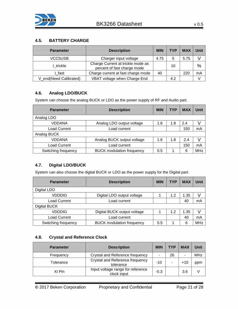
4.5. BATTERY CHARGE
Parameter Description MIN TYP MAX Unit
VCC5USB Charger input voltage 4.75 5 5.75 V I_trickle Charge Current at trickle mode as
percent of fast charge mode 10 % I_fast Charge current at fast charge mode 40 220 mA
V_end(Need Calibrated) VBAT voltage when Charge End 4.2 V
4.6. Analog LDO/BUCK System can choose the analog BUCK or LDO as the power supply of RF and Audio part.
Parameter Description MIN TYP MAX Unit
Analog LDO VDDANA Analog LDO output voltage 1.6 1.8 2.4 V
Load Current Load current 150 mA Analog BUCK
VDDANA Analog BUCK output voltage 1.6 1.8 2.4 V Load Current Load current 150 mA
Switching frequency BUCK modulation frequency 0.5 1 6 MHz
4.7. Digital LDO/BUCK System can also choose the digital BUCK or LDO as the power supply for the Digital part.
Parameter Description MIN TYP MAX Unit
Digital LDO VDDDIG Digital LDO output voltage 1 1.2 1.35 V
Load Current Load current 40 mA Digital BUCK
VDDDIG Digital BUCK output voltage 1 1.2 1.35 V Load Current Load current 40 mA
Switching frequency BUCK modulation frequency 0.5 1 6 MHz
4.8. Crystal and Reference Clock
Parameter Description MIN TYP MAX Unit
Frequency Crystal and Reference frequency - 26 - MHz
Tolerance Crystal and Reference frequency tolerance -10 - +10 ppm
XI Pin Input voltage range for reference clock input -0.3 3.6 V
Low Power Bluetooth Audio SoC v 0.5
© 2017 Beken Corporation Proprietary and Confidential Page 22 of 28
4.9. Typical Power Consumption
State Description MIN TYP MAX Unit
Shut Down Software sets device into shut down mode, wake up from GPIO15 0.4 0.8 uA
Standby Software sets device into standby mode, wake up from GPIO and RTC timer 4 6 uA
Idle-Sniff Idle state at Sniff mode 300 uA Active (A2DP) 2DH5 9 mA Active (HFP) HV1 9.5 mA
4.10. RF Characteristics
Parameter Condition MIN TYP MAX Unit
Operate Frequency 2402~2480 2402 2480 MHz RXSENS-1 Mbps BER=0.001 -88 dBm RXSENS-2 Mbps BER=0.0001 -91 dBm RXSENS-3 Mbps BER=0.0001 -83 dBm
Maximum received signal BER=0.001 0 dBm Maximum RF transmit
power 8 dBm
RF Power Control Range 30 dB
4.11. Audio Characteristics
Parameter Condition MIN TYP MAX Unit
DAC Diff. Output With 600ohm loading 1.1 Vrms With 32ohm loading - - Vrms With 16ohm loading 0.9 Vrms
DAC Diff. Output THD With 1.1Vrms@600ohm loading 75 dB With 0.8Vrms@16ohm loading 75 dB
DAC output SNR 1 kHz sine wave 98 dB DAC Sample Rate 8 48 kHz
ADC SNR 1 kHz sine wave 96 dB ADC Sample Rate 8 48 kHz
BK3266 Datasheet v 0.5
© 2017 Beken Corporation Proprietary and Confidential Page 23 of 28
5. About Qualification By carefully laying out the printed circuit board (PCB), the BK3266 RF performance meets FCC, CE and BQB requirement. The Bluetooth protocol and profile provided by Beken are already qualified and listed in the SIG website. If there is any end product listing requirement with the BK3266, please inquire your local Beken Corporation representative for the related QDID authorization.

Low Power Bluetooth Audio SoC v 0.5
© 2017 Beken Corporation Proprietary and Confidential Page 24 of 28
6. Package Information
6.1. QFN 4x4 32-pin package

BK3266 Datasheet v 0.5
© 2017 Beken Corporation Proprietary and Confidential Page 25 of 28
6.2. TSSOP28 package

Low Power Bluetooth Audio SoC v 0.5
© 2017 Beken Corporation Proprietary and Confidential Page 26 of 28
6.3. QFN 5x5 40-pin package

BK3266 Datasheet v 0.5
© 2017 Beken Corporation Proprietary and Confidential Page 27 of 28
6.4. SOP16 package

Low Power Bluetooth Audio SoC v 0.5
© 2017 Beken Corporation Proprietary and Confidential Page 28 of 28
7. Ordering Information
Part number Package Packing MOQ (ea) BK3266QN32 QFN 4mmx4mm 32-Pin Tape Reel 3 k BK3266TS28 TSSOP 28-Pin Tube - BK3266QN40 QFN 5mmx5mm 40-Pin Tape Reel 3 k BK3266SO16A SOP 16-Pin Tube - BK3266SO16B SOP 16-Pin Tube -
Remark: MOQ: Minimum Order Quantity