Embed Size (px)
Citation preview
BIT ERROR RATE MONITORING
FOR A SONET/SDH FRAMER
by
Robert Trost
A THESIS SUBMITTED IN PARTIAL FULFILLMENT OF THE REQUIREMENTS FOR THE DEGREE OF
BACHELOR OF APPLIED SCIENCE In the School
of Engineering Science
Robert Trost 2001 West Bay Semiconductor Inc.
April 1, 2001
All rights reserved. This work may not be reproduced in whole or in part, by photocopy or other means, without
permission of the author.
ii
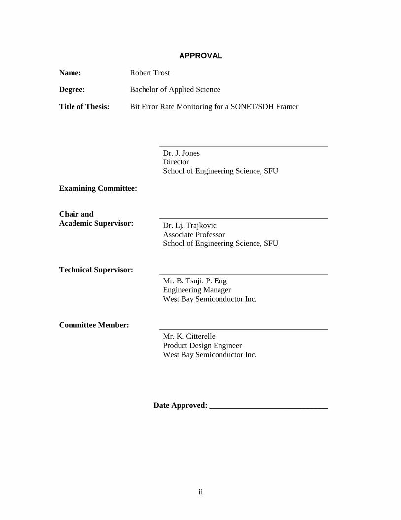
APPROVAL
Name: Robert Trost
Degree: Bachelor of Applied Science
Title of Thesis: Bit Error Rate Monitoring for a SONET/SDH Framer
Dr. J. Jones
Director School of Engineering Science, SFU
Examining Committee:
Chair and
Academic Supervisor: Dr. Lj. Trajkovic Associate Professor School of Engineering Science, SFU
Technical Supervisor: Mr. B. Tsuji, P. Eng Engineering Manager West Bay Semiconductor Inc.
Committee Member: Mr. K. Citterelle Product Design Engineer West Bay Semiconductor Inc.
Date Approved: ______________________________
iii
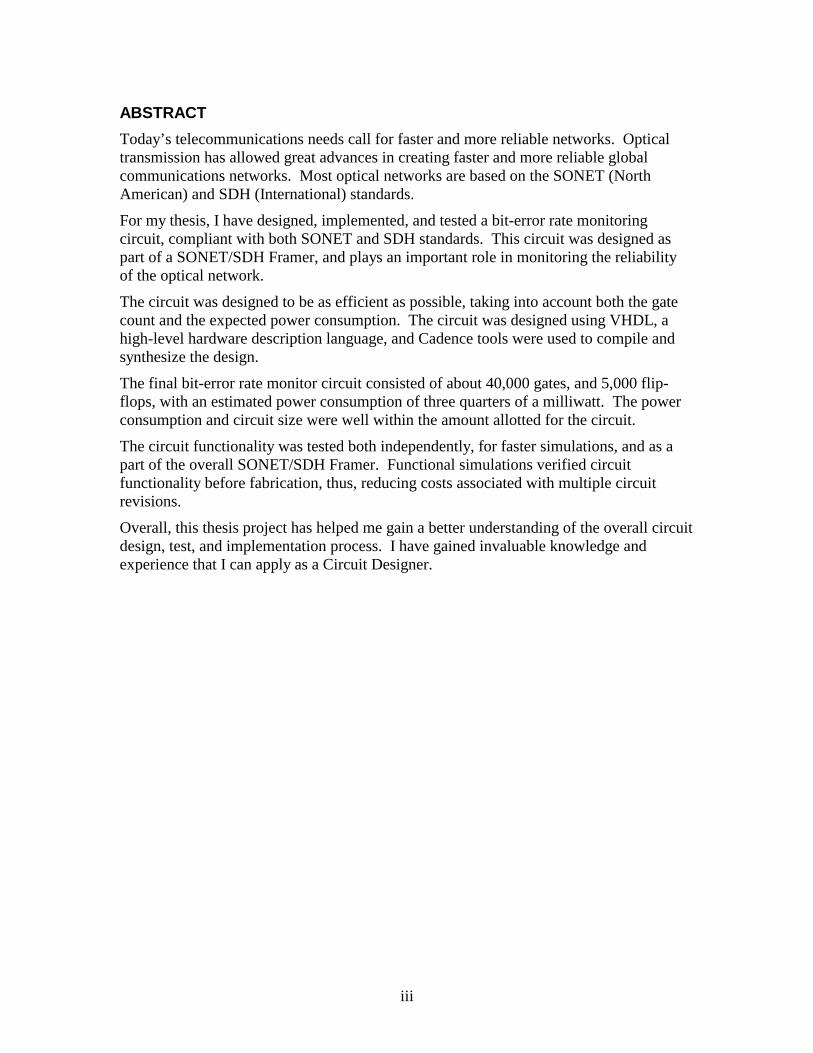
ABSTRACT Today’s telecommunications needs call for faster and more reliable networks. Optical transmission has allowed great advances in creating faster and more reliable global communications networks. Most optical networks are based on the SONET (North American) and SDH (International) standards.
For my thesis, I have designed, implemented, and tested a bit-error rate monitoring circuit, compliant with both SONET and SDH standards. This circuit was designed as part of a SONET/SDH Framer, and plays an important role in monitoring the reliability of the optical network.
The circuit was designed to be as efficient as possible, taking into account both the gate count and the expected power consumption. The circuit was designed using VHDL, a high-level hardware description language, and Cadence tools were used to compile and synthesize the design.
The final bit-error rate monitor circuit consisted of about 40,000 gates, and 5,000 flip-flops, with an estimated power consumption of three quarters of a milliwatt. The power consumption and circuit size were well within the amount allotted for the circuit.
The circuit functionality was tested both independently, for faster simulations, and as a part of the overall SONET/SDH Framer. Functional simulations verified circuit functionality before fabrication, thus, reducing costs associated with multiple circuit revisions.
Overall, this thesis project has helped me gain a better understanding of the overall circuit design, test, and implementation process. I have gained invaluable knowledge and experience that I can apply as a Circuit Designer.

iv
ACKNOWLEDGMENTS I would like to offer many thanks to Barry Tsuji, Ljiljana Trajkovic and Kevin Citterelle for serving on my thesis committee, as well as Steve Whitmore for editing this document. I would also like to thank everyone at West Bay Semiconductor for their assistance in putting together this thesis. Special thanks go to my wife, Elia Robles, for her support.
PRIVATE AND CONFIDENTIAL v
TABLE OF CONTENTS APPROVAL ....................................................................................................................... ii ABSTRACT....................................................................................................................... iii ACKNOWLEDGMENTS ................................................................................................. iv LIST OF FIGURES ........................................................................................................... vi LIST OF TABLES............................................................................................................. vi GLOSSARY OF ACRONYMS........................................................................................ vii 1 Introduction................................................................................................................. 1 2 A SONET Primer........................................................................................................ 1
2.1 SONET Frame Structure..................................................................................... 2 2.2 SONET Transport Overhead............................................................................... 3 2.3 The B2 Line Overhead Byte ............................................................................... 4
3 SONET Bit-Error Rate Monitoring Requirements ..................................................... 4 3.1 Statistical Model for Bit-Error Rate Monitoring ................................................ 6 3.2 Determining Bit-Error Rate Monitoring Thresholds .......................................... 7
4 System Design ............................................................................................................ 8 4.1 The SONET Framer............................................................................................ 8 4.2 The Bit-Error Rate Monitoring Circuit ............................................................... 9 4.3 Bit Error Rate Monitor Functional Design ....................................................... 11 4.4 Bit-Error Rate Monitor Architecture ................................................................ 12
4.4.1 Controller Circuitry................................................................................... 13 4.4.2 Adder and Mux ......................................................................................... 13 4.4.3 Register Bank............................................................................................ 14 4.4.4 Computational Unit................................................................................... 15
5 Circuit Implementation ............................................................................................. 17 5.1 Synthesis ........................................................................................................... 17 5.2 Power Consumption.......................................................................................... 18
6 Circuit Testing .......................................................................................................... 18 6.1 Circuit-Level Simulations................................................................................. 19 6.2 Top-Level Simulation ....................................................................................... 21
7 Conclusion ................................................................................................................ 22 References......................................................................................................................... 23

PRIVATE AND CONFIDENTIAL vi
LIST OF FIGURES Figure 1 – SONET STS-1 Frame........................................................................................ 2 Figure 2 – SONET STS-1 Overhead Bytes. ....................................................................... 3 Figure 3 – SONET STS-N Overhead Bytes. ...................................................................... 4 Figure 4 – Block Diagram of SONET/SDH Framer with Bit-Error Rate Monitoring ....... 9 Figure 5 – Bit-Error Rate Monitoring Circuitry ................................................................. 9 Figure 6 – Sliding Window to Detect SF/SD Bit Error Rate Conditions ......................... 11 Figure 7 – Block Diagram of Bit-Error Rate Monitoring Circuit Architecture................ 12 Figure 8 – Pseudocode for Bit-Error Rate Monitor Controller......................................... 13 Figure 9 – Pseudocode for BIP Count Adder. .................................................................. 14 Figure 10 – Pseudocode for Computational Unit. ............................................................ 16 Figure 11 – Block Diagram of Circuit-Level Test-Bench ................................................ 19
LIST OF TABLES Table 1 – SONET Line Rates. ............................................................................................ 2 Table 2 – Maximum/Objective Bit-Error Rate Detection/Clearing Times......................... 5 Table 3 – Probability of BIP Errors for Bit-Error Rate Between 10-3 and 10-9 .................. 6 Table 4 – STS-3/12/48 Detection and Clearing Line Bit-Error Rate Thresholds............... 8 Table 5 –Bit-Error Rate Monitoring Circuit Port Descriptions ........................................ 10 Table 6 – Registers for Storing Bit-Error Rate Monitoring Data. .................................... 15 Table 7 – Power Calculation............................................................................................. 18
PRIVATE AND CONFIDENTIAL vii
GLOSSARY OF ACRONYMS ANSI – American Standards Institute
BIP – Bit-Interleaved Parity
CCITT – Consultative Committee on International Telegraphy and Telephony
EDA – Electronic Design Automation
IC – Integrated Circuit
ITU – International Telecommunications Union
OC – Optical Carrier
SDH – Synchronous Digital Hierarchy
SD – Signal Degrade
SF – Signal Failure
SONET – Synchronous Optical Network
STS – Synchronous Transport Signal
VHDL – VHSIC Hardware description Language
VHSIC – Very High Speed Integrated Circuit

. PRIVATE AND CONFIDENTIAL 1
1 Introduction Over the last 100 years, communications networks have evolved from analog telephone and radio signals to the modern digital network. These digital networks are required to carry large amounts of data at high rates. The need for increased bandwidth has caused an evolution in the media from wires and air, to optical fibers, which provide for fast communications and improved quality of service. The SONET standard provides for an economic, flexible, and compatible solution for optical transmission.
One of the advantages of SONET, and optical networks in general, is the low bit error rates that are achieved. A thousand times improvement in bit error rate can be achieved when changing from coax or twisted pair to optical fiber (Chow, 1995, 1-23). For my thesis, I have designed, implemented, and tested a bit-error rate monitoring circuit. The circuit might be used in a SONET/SDH Framer, part of West Bay Semiconductor’s new high density SONET solutions.
Bit-error rate monitoring plays an important role in measuring the quality of service delivered by a network. Service providers must guarantee data integrity to their clients, and the bit-error rate measurement is used to measure it. Thus, bit-error rate monitoring circuitry plays an integral role in a SONET/SDH Framer.
An important aspect of the bit-error rate circuit that I have designed is that it is able to operate at a variety of SONET/SDH line rates. In order to increase reusability of the circuit, it has been designed to work in SONET/SDH Framers operating at several line rates in the SONET/SDH hierarchy, as described in Section 2.
2 A SONET Primer SONET (Synchronous Optical Network) is a standard for optical transport formulated for the American National Standards Institute (ANSI), which sets industry standards in the U.S. for telecommunications and other industries. The standard has also been incorporated into the Synchronous Digital Hierarchy (SDH) recommendations of the Consultative Committee on International Telegraphy and Telephony (CCITT) (now called the International Telecommunications Union [ITU]), which sets standards for international telecommunications. However, SONET and SDH are technically consistent, with the major difference being in the terminology used to describe the standards. For the purpose of my thesis, I intend to use the SONET terminology to remain consistent, however, the circuit must be compliant with both SONET/SDH standards (Kartalopoulos, 1999, 32).
SONET defines optical carrier (OC) levels and electrically equivalent synchronous transport signals (STS’s) for the fiber-optic based transmission hierarchy. The standard SONET line rates and STS-equivalent formats are shown in Table 1. The fiber-optic rates shown in bold must be supported by the bit error rate monitoring circuit.
. PRIVATE AND CONFIDENTIAL 2
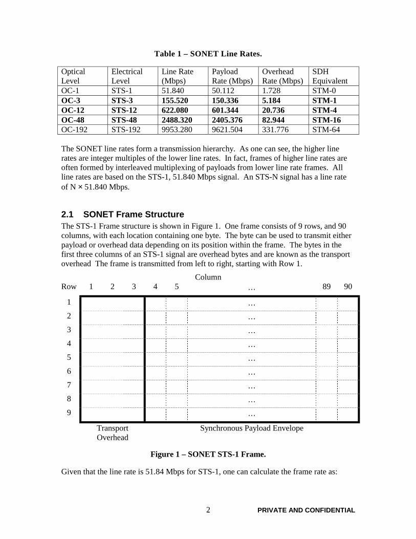
Table 1 – SONET Line Rates.
Optical Level
Electrical Level
Line Rate (Mbps)
Payload Rate (Mbps)
Overhead Rate (Mbps)
SDH Equivalent
OC-1 STS-1 51.840 50.112 1.728 STM-0 OC-3 STS-3 155.520 150.336 5.184 STM-1 OC-12 STS-12 622.080 601.344 20.736 STM-4 OC-48 STS-48 2488.320 2405.376 82.944 STM-16 OC-192 STS-192 9953.280 9621.504 331.776 STM-64 The SONET line rates form a transmission hierarchy. As one can see, the higher line rates are integer multiples of the lower line rates. In fact, frames of higher line rates are often formed by interleaved multiplexing of payloads from lower line rate frames. All line rates are based on the STS-1, 51.840 Mbps signal. An STS-N signal has a line rate of N × 51.840 Mbps.
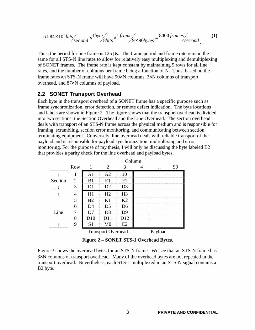
2.1 SONET Frame Structure The STS-1 Frame structure is shown in Figure 1. One frame consists of 9 rows, and 90 columns, with each location containing one byte. The byte can be used to transmit either payload or overhead data depending on its position within the frame. The bytes in the first three columns of an STS-1 signal are overhead bytes and are known as the transport overhead The frame is transmitted from left to right, starting with Row 1.
Column Row 1 2 3 4 5 … 89 90
1 …
2 …
3 …
4 …
5 …
6 …
7 …
8 …
9 …
Transport Overhead
Synchronous Payload Envelope
Figure 1 – SONET STS-1 Frame.
Given that the line rate is 51.84 Mbps for STS-1, one can calculate the frame rate as:
. PRIVATE AND CONFIDENTIAL 3
ondframes
bytesframe
bitsbyte
ondbits
sec8000
9091
81
sec1084.51 6
=××××. (1)
Thus, the period for one frame is 125 µs. The frame period and frame rate remain the same for all STS-N line rates to allow for relatively easy multiplexing and demultiplexing of SONET frames. The frame rate is kept constant by maintaining 9 rows for all line rates, and the number of columns per frame being a function of N. Thus, based on the frame rates an STS-N frame will have 90×N columns, 3×N columns of transport overhead, and 87×N columns of payload.
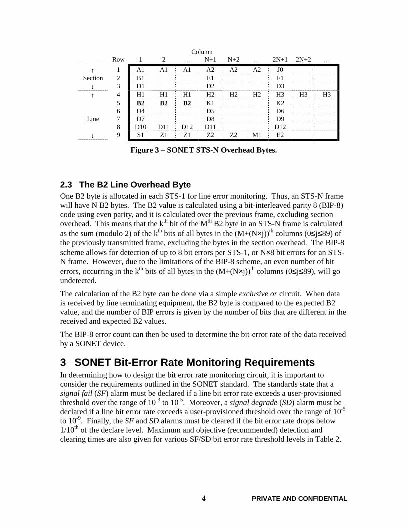
2.2 SONET Transport Overhead Each byte in the transport overhead of a SONET frame has a specific purpose such as frame synchronization, error detection, or remote defect indication. The byte locations and labels are shown in Figure 2. The figure shows that the transport overhead is divided into two sections: the Section Overhead and the Line Overhead. The section overhead deals with transport of an STS-N frame across the physical medium and is responsible for framing, scrambling, section error monitoring, and communicating between section terminating equipment. Conversely, line overhead deals with reliable transport of the payload and is responsible for payload synchronization, multiplexing and error monitoring. For the purpose of my thesis, I will only be discussing the byte labeled B2 that provides a parity check for the line overhead and payload bytes.
Column Row 1 2 3 4 … 90
↑ 1 A1 A2 J0 Section 2 B1 E1 F1
↓ 3 D1 D2 D3 ↑ 4 H1 H2 H3 5 B2 K1 K2 6 D4 D5 D6
Line 7 D7 D8 D9 8 D10 D11 D12
↓ 9 S1 M0 E2 Transport Overhead Payload
Figure 2 – SONET STS-1 Overhead Bytes.
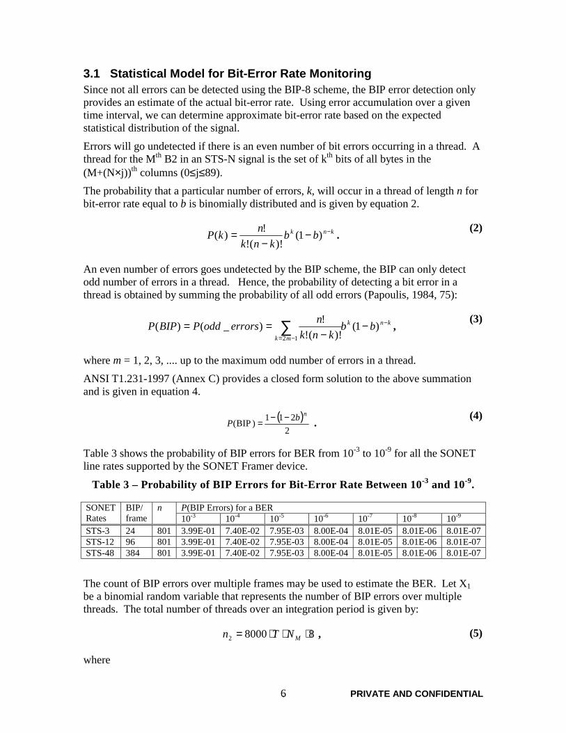
Figure 3 shows the overhead bytes for an STS-N frame. We see that an STS-N frame has 3×N columns of transport overhead. Many of the overhead bytes are not repeated in the transport overhead. Nevertheless, each STS-1 multiplexed in an STS-N signal contains a B2 byte.
. PRIVATE AND CONFIDENTIAL 4
Column Row 1 2 … N+1 N+2 … 2N+1 2N+2 …
↑ 1 A1 A1 A1 A2 A2 A2 J0 Section 2 B1 E1 F1
↓ 3 D1 D2 D3 ↑ 4 H1 H1 H1 H2 H2 H2 H3 H3 H3 5 B2 B2 B2 K1 K2 6 D4 D5 D6
Line 7 D7 D8 D9 8 D10 D11 D12 D11 D12
↓ 9 S1 Z1 Z1 Z2 Z2 M1 E2
Figure 3 – SONET STS-N Overhead Bytes.
2.3 The B2 Line Overhead Byte One B2 byte is allocated in each STS-1 for line error monitoring. Thus, an STS-N frame will have N B2 bytes. The B2 value is calculated using a bit-interleaved parity 8 (BIP-8) code using even parity, and it is calculated over the previous frame, excluding section overhead. This means that the kth bit of the Mth B2 byte in an STS-N frame is calculated as the sum (modulo 2) of the kth bits of all bytes in the (M+(N×j))th columns (0≤j≤89) of the previously transmitted frame, excluding the bytes in the section overhead. The BIP-8 scheme allows for detection of up to 8 bit errors per STS-1, or N×8 bit errors for an STS-N frame. However, due to the limitations of the BIP-8 scheme, an even number of bit errors, occurring in the kth bits of all bytes in the (M+(N×j))th columns (0≤j≤89), will go undetected.
The calculation of the B2 byte can be done via a simple exclusive or circuit. When data is received by line terminating equipment, the B2 byte is compared to the expected B2 value, and the number of BIP errors is given by the number of bits that are different in the received and expected B2 values.
The BIP-8 error count can then be used to determine the bit-error rate of the data received by a SONET device.
3 SONET Bit-Error Rate Monitoring Requirements In determining how to design the bit error rate monitoring circuit, it is important to consider the requirements outlined in the SONET standard. The standards state that a signal fail (SF) alarm must be declared if a line bit error rate exceeds a user-provisioned threshold over the range of 10-3 to 10-5. Moreover, a signal degrade (SD) alarm must be declared if a line bit error rate exceeds a user-provisioned threshold over the range of 10-5 to 10-9. Finally, the SF and SD alarms must be cleared if the bit error rate drops below 1/10th of the declare level. Maximum and objective (recommended) detection and clearing times are also given for various SF/SD bit error rate threshold levels in Table 2.

. PRIVATE AND CONFIDENTIAL 5
Table 2 – Maximum/Objective Bit-Error Rate Detection/Clearing Times.
SD/SF BER Threshold
10-3 10-4 10-5 10-6 10-7 10-8 10-9
Clearing BER Threshold
10-4 10-5 10-6 10-7 10-8 10-9 10-10
Max. Detection and Clearing Time (s)
0.01 0.1 1 10 100 1000 10000
STS-3 0.008/ none
0.13/ none
0.1/ none
1.0/ none
10/ 83
83/ 667
667/ 5360
STS-12 0.008/ none
0.008/ 0.025
0.025/ 0.25
0.25/ 2.5
2.5/ 21
21/ 167
167/ 1330
Objective Detection/ Clearing Time (s)
STS-48 0.008/ none
0.008/ 0.01
0.008/ 0.0625
0.0625/ 0.625
0.625/ 5.2
5.2/ 42
42/ 340
Moreover, the SONET standard contains detection, false detection, clearing, and false clearing requirements for both SD and SF conditions as follows:
Detection requirement: A 10-x bit-error rate detection time will be less than maximum detection time (GR-253 R5-44).
Objective detection requirement: the probability of the 10-x bit-error rate detection time will be less than objective detection time should be ≥ 0.95 (GR-253 O5-45). False detection requirement: for a bit-error rate detection threshold of 10-x and an actual bit-error rate of 10-(x+1), the probability the bit-error rate detected in the maximum detection time shall be ≤ 10-6 (GR-253 R5-46).
Clearing requirement: If a bit-error rate condition has been detected and the incoming signal’s bit-error rate is ≤ 10–(x+1), the probability that the detector will detect the bit-error rate is less than the clearing threshold within the maximum clearing time shall be ≥ 0.99 (GR-253 R5-51).
Objective clearing requirement: If the bit-error rate condition has been detected and the incoming signal’s bit-error rate is ≤ 10–(x+1), the probability that the detector will detect the bit-error rate is less than the clearing threshold within the objective clearing time should be ≥ 0.95 (GR-253 O5-53).
False clearing requirement: If a bit-error rate condition has been detected and the incoming signal’s bit-error rate is ≥ 10–x, the probability that the detector will detect the bit-error rate is less than the clearing threshold within the maximum clearing time shall be ≤ 10-6 (GR-253 R5-52).
In the above x = 3, 4 or 5 is defined for line SF and x = 5, 6, 7, 8 or 9 is defined for line SD.
In order to apply the SONET criteria for declaring and clearing of SD and SF conditions, we must derive a statistical model for the bit-error rate.
. PRIVATE AND CONFIDENTIAL 6
3.1 Statistical Model for Bit-Error Rate Monitoring Since not all errors can be detected using the BIP-8 scheme, the BIP error detection only provides an estimate of the actual bit-error rate. Using error accumulation over a given time interval, we can determine approximate bit-error rate based on the expected statistical distribution of the signal.
Errors will go undetected if there is an even number of bit errors occurring in a thread. A thread for the Mth B2 in an STS-N signal is the set of kth bits of all bytes in the (M+(N×j))th columns (0≤j≤89). The probability that a particular number of errors, k, will occur in a thread of length n for bit-error rate equal to b is binomially distributed and is given by equation 2.
knk bbknk
nkP −−−
= )1()!(!
!)( . (2)
An even number of errors goes undetected by the BIP scheme, the BIP can only detect odd number of errors in a thread. Hence, the probability of detecting a bit error in a thread is obtained by summing the probability of all odd errors (Papoulis, 1984, 75):
knk
mkbb
knknerrorsoddPBIPP −
−=
−−
== ∑ )1()!(!
!)_()(12
, (3)
where m = 1, 2, 3, .... up to the maximum odd number of errors in a thread.
ANSI T1.231-1997 (Annex C) provides a closed form solution to the above summation and is given in equation 4.
( )2
211) BIP(nbP −−= . (4)
Table 3 shows the probability of BIP errors for BER from 10-3 to 10-9 for all the SONET line rates supported by the SONET Framer device.
Table 3 – Probability of BIP Errors for Bit-Error Rate Between 10-3 and 10-9.
P(BIP Errors) for a BER SONET Rates
BIP/ frame
n 10-3 10-4 10-5 10-6 10-7 10-8 10-9
STS-3 24 801 3.99E-01 7.40E-02 7.95E-03 8.00E-04 8.01E-05 8.01E-06 8.01E-07 STS-12 96 801 3.99E-01 7.40E-02 7.95E-03 8.00E-04 8.01E-05 8.01E-06 8.01E-07 STS-48 384 801 3.99E-01 7.40E-02 7.95E-03 8.00E-04 8.01E-05 8.01E-06 8.01E-07
The count of BIP errors over multiple frames may be used to estimate the BER. Let X1 be a binomial random variable that represents the number of BIP errors over multiple threads. The total number of threads over an integration period is given by:
880002 ⋅⋅⋅= MNTn , (5)
where
. PRIVATE AND CONFIDENTIAL 7
T = integration period in seconds, NM = the hierarchy level N in STS-N.
Assuming the bit errors in any thread of a frame are independent and at the same time the bit errors in the threads in different frames are independent, the probability of k2 BIP errors in the integration period is given by the binomial distribution (Papoulis, 1984, 75):
( ) ( ) ( ) 222 )(1)(!!
!
222
221
knk BIPPBIPPknk
nkXP −−
−== . (6)
Since n2 is sufficiently large, central limit theorem applies, and the above distribution can be approximated by a normal distribution (Papoulis, 1984, 194):
( )( )
2
22
221
21 p
pk
p
ekXP σ
µ
σπ
−−
≅= . (7)
The mean and variance are given by:
( )( ) ( )( )BIP1BIP
BIP
22
2
PPn
Pn
p
p
−××=
×=
σ
µ .
(8)
A 100 × (1 - α) % confidence interval to estimate a normal distribution with mean µ and standard deviation σ is therefore given by:
⋅+⋅− pppp zz σµσµ αα22
, . (9)
The one-sided 95%, 99% and 99.9999% confidence limits where α/2 = 0.05, 0.01 and 0.000001 are found to be: ±1.645, ±2.326 and ±4.768. These three values are used later to deduce the thresholds for different BER.
3.2 Determining Bit-Error Rate Monitoring Thresholds In order to detect a SD or SF condition, the objective detection threshold must be chosen so that the confidence level of detection must be ≥ 95% when the actual bit-error rate condition is present. Alternatively, to clear a SD or SF condition when the cumulated BIP count is less than the threshold over the objective measuring time interval, the objective clearing threshold must be chosen such that the confidence level of clearing must be ≥ 95% when the actual BER condition is absent. The criteria for the remaining four threshold values, mentioned in section 3, can be defined similarly.

. PRIVATE AND CONFIDENTIAL 8
We can derive error thresholds by applying the statistical model for BIP-8 detection at various bit-error rates to the SONET detection and clearing requirements. Table 4 shows the BIP-8 error thresholds necessary to declare or clear SD/SF alarms at various bit-error rates. All thresholds are determined over the objective declaration or clearing periods except for those marked with an asterisk, which have no objective period. For those entries with no objective clearing/detecting time, the maximum time was used.
Table 4 – STS-3/12/48 Detection and Clearing Line Bit-Error Rate Thresholds.
Bit-Error Rate Threshold Limits SONET Rates
10-3 10-4 10-5 10-6 10-7 10-8 10-9
Detect Thresh.
581 163 132 133 133 109 85 STS-3
Clear Thresh.
169* 182* 183* 183* 147 120 98
Detect Thresh.
2390 421 132 133 133 110 86 STS-12
Clear Thresh.
622* 173 175 175 148 120 97
Detect Thresh.
9689 1751 172 133 133 109 86 STS-48
Clear Thresh.
2381* 270 175 175 147 121 99
These values for bit-error rate thresholds will be applied when determining the maximum register sizes for the user provisionable settings of the bit-error rate monitoring circuitry.
4 System Design 4.1 The SONET Framer The SONET Framer for which the bit-error rate circuitry has been designed is scalable. This means that the framer, and in turn, the bit-error rate circuitry, is designed to operate at various line rates. As mentioned previously, these line rates are STS-3, STS-12, and STS-48. However, the total bandwidth handled by the device remains constant as the framer can handle up to 16 lines simultaneously in STS-3 mode, 4 lines in STS-12 mode, and 1 line in STS-48.
The SONET Framer receives raw data in the form of electrical pulses, performs clock and data recovery on the signal, and synchronizes to the A1/A2 framing bytes in the section overhead (see Figure 3). As the frame overhead and data are processed, a BIP-8 count is kept and compared to the B2 value in the line overhead to detect bit-errors. The number of detected errors is then used by the bit-error rate monitoring block to determine if a Signal Degrade or Signal Failure condition, as defined in the SONET standard, is to be declared. If an SD or SF condition is met, the bit-error rate monitoring block generates an alarm signal that is transmitted with the data to indicate poor data integrity to downstream devices. Moreover, an output status signal from the SONET Framer will
. PRIVATE AND CONFIDENTIAL 9
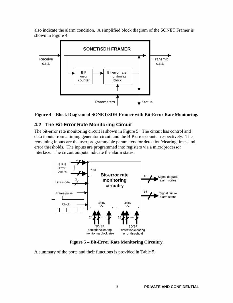
also indicate the alarm condition. A simplified block diagram of the SONET Framer is shown in Figure 4.
BIP error
counter
Bit error rate monitoring
block
Receive data
Transmit data
Parameters Status
SONET/SDH FRAMER
Figure 4 – Block Diagram of SONET/SDH Framer with Bit-Error Rate Monitoring.
4.2 The Bit-Error Rate Monitoring Circuit The bit-error rate monitoring circuit is shown in Figure 5. The circuit has control and data inputs from a timing generator circuit and the BIP error counter respectively. The remaining inputs are the user programmable parameters for detection/clearing times and error thresholds. The inputs are programmed into registers via a microprocessor interface. The circuit outputs indicate the alarm states.
BIP-8 error
counts 48
Frame pulse
Clock
16
16
15 24
4×16 4×16
SD/SF detection/clearing
monitoring block size
SD/SF detection/clearing
error threshold
Line mode 2
Signal degrade alarm status
Signal failure alarm status
Bit-error rate monitoring
circuitry
4
Figure 5 – Bit-Error Rate Monitoring Circuitry.
A summary of the ports and their functions is provided in Table 5.

. PRIVATE AND CONFIDENTIAL 10
Table 5 –Bit-Error Rate Monitoring Circuit Port Descriptions.
Port Name Port Type
Port Description Number of ports
Width of port (bits)
BIP-8 error count
Input BIP-8 error counts. Values range from 0 to 8. Note there are N BIP-8 counts per STS-N signal.
48 4
Line mode Input Two bits to determine if device is to operate in 16 STS-3, 4 STS-12, or one STS-48 line mode.
1 2
Frame pulse Input Pulse lasting one clock period repeated every 125 µs.
1 1
Clock Input 19.44 MHz clock. 1 1
SD detection monitoring block size
Input 24-bit user provisioned parameter to determine the monitoring block size for Signal Degrade detection.
16 24
SD clearing monitoring block size
Input 24-bit user provisioned parameter to determine the monitoring block size for Signal Degrade clearing.
16 24
SF detection monitoring block size
Input 24-bit user provisioned parameter to determine the monitoring block size for Signal Failure detection.
16 24
SF clearing monitoring block size
Input 24-bit user provisioned parameter to determine the monitoring block size for Signal Failure clearing.
16 24
SD detection error threshold
Input 15-bit user provisioned error threshold parameter for Signal Degrade detection.
16 15
SD clearing error threshold
Input 15-bit user provisioned error threshold parameter for Signal Degrade clearing.
16 15
SF detection error threshold
Input 15-bit user provisioned error threshold parameter for Signal Failure detection.
16 15
SF clearing error threshold
Input 15-bit user provisioned error threshold parameter for Signal Failure clearing.
16 15
SD alarm status Output Signal degrade status for each line. 16 1
SF alarm status Output Signal failure status for each line. 16 1
Note that the circuit has 48 BIP-8 error count inputs, resulting from the fact that there are 48 B2 bytes per frame in sixteen STS-3 signals, four STS-12 signals, or one STS-48 signal. The two-bit line mode input determines which of the three modes the circuit will
. PRIVATE AND CONFIDENTIAL 11
operate in. The input clock is a 19.44 MHz clock, and the frame pulse input is strobed ‘hi’ every 125 µs after all of the 48 BIP-8 counts have been updated by the BIP error counting circuitry. For each line, we require four monitoring block size parameters and four error threshold parameters since detection and clearing for signal degrade and signal failure are independent. Thus, we need 64 detection/clearing time parameters, and 64 error threshold parameters for the sixteen STS-3 line mode. In the four STS-12 line mode, we only require the 16 values, and in one STS-48 line mode, only 4 input parameters for the clearing/detection time and error threshold are necessary. These parameters are programmed into on-chip registers via the SONET Framer’s microprocessor interface.
Finally, the outputs of the chip indicate whether a given line is in SD or SF alarm state. This signal is used to introduce alarm indication signals into the data stream as well as to cause a hardware interrupt.
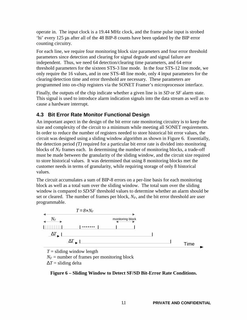
4.3 Bit Error Rate Monitor Functional Design An important aspect in the design of the bit error rate monitoring circuitry is to keep the size and complexity of the circuit to a minimum while meeting all SONET requirements. In order to reduce the number of registers needed to store historical bit error values, the circuit was designed using a sliding window algorithm as shown in Figure 6. Essentially, the detection period (T) required for a particular bit error rate is divided into monitoring blocks of NF frames each. In determining the number of monitoring blocks, a trade-off must be made between the granularity of the sliding window, and the circuit size required to store historical values. It was determined that using 8 monitoring blocks met the customer needs in terms of granularity, while requiring storage of only 8 historical values.
The circuit accumulates a sum of BIP-8 errors on a per-line basis for each monitoring block as well as a total sum over the sliding window. The total sum over the sliding window is compared to SD/SF threshold values to determine whether an alarm should be set or cleared. The number of frames per block, NF, and the bit error threshold are user programmable.
T ∆ T ∆
F N 8 T × =
F N
Time
monitoring block
T = sliding window length NF = number of frames per monitoring block ∆T = sliding delta
Figure 6 – Sliding Window to Detect SF/SD Bit-Error Rate Conditions.
. PRIVATE AND CONFIDENTIAL 12
In Table 5, it is shown that NF, the number of frames per monitoring block, which determines detection and clearing times, requires a 24 bits wide parameter. The number of bits required is determined from the SONET standard which allows for a maximum sliding window length of 10,000 seconds. At a rate of 8,000 frames/second, we would have a maximum detection/clearing period (T) of 80 million frames, thus the maximum number of frames per monitoring block would be 10 million frames. Since 224=16,777,216, the fewest number of bits necessary to represent the maximum NF value is 24 bits.
Moreover, in Table 4, we see that the greatest detection/clearing error threshold is 9,689 bit errors, which indicates that a 14-bit (214=16,384) threshold value would suffice. However, the threshold values in Table 4 are given for the objective detection/clearing times, and in order to meet the maximum time criteria, we need error thresholds as high as 23,692, thus requiring a 15-bit threshold value (215=32,768). That being said, the SF/SD clearing threshold values only require 13-bit values since they are a factor of 10 lower than the declare thresholds, as stated in the SONET standards.
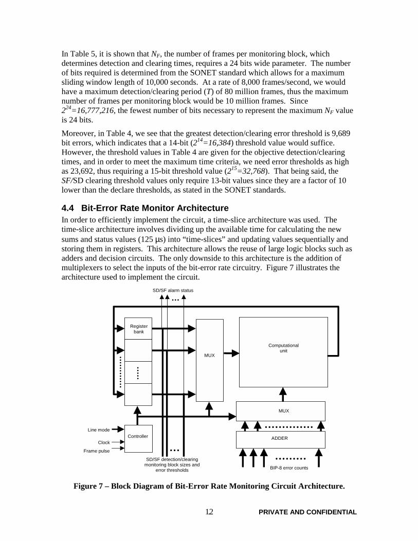
4.4 Bit-Error Rate Monitor Architecture In order to efficiently implement the circuit, a time-slice architecture was used. The time-slice architecture involves dividing up the available time for calculating the new sums and status values (125 µs) into “time-slices” and updating values sequentially and storing them in registers. This architecture allows the reuse of large logic blocks such as adders and decision circuits. The only downside to this architecture is the addition of multiplexers to select the inputs of the bit-error rate circuitry. Figure 7 illustrates the architecture used to implement the circuit.
Controller
MUX
Computational unit
SD/SF alarm status
Register bank
BIP-8 error counts
MUX
Line mode
Frame pulse
Clock ADDER
SD/SF detection/clearing monitoring block sizes and
error thresholds Figure 7 – Block Diagram of Bit-Error Rate Monitoring Circuit Architecture.
. PRIVATE AND CONFIDENTIAL 13
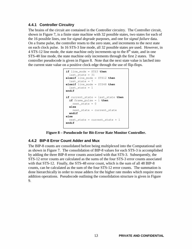
4.4.1 Controller Circuitry The brains of the circuit are contained in the Controller circuitry. The Controller circuit, shown in Figure 7, is a finite state machine with 32 possible states, two states for each of the 16 possible lines, one for signal degrade purposes, and one for signal failure data. On a frame pulse, the controller resets to the zero state, and increments to the next state on each clock pulse. In 16 STS-3 line mode, all 32 possible states are used. However, in 4 STS-12 line mode, the state machine only increments up to the 8th state, and in one STS-48 line mode, the state machine only increments through the first 2 states. The controller pseudocode is given in Figure 8. Note that the next state value is latched into the current state value on a positive clock edge through the use of flip-flops.
if line_mode = STS3 then last_state = 31 elseif line_mode = STS12 then last_state = 7 elseif line_mode = STS48 then last_state = 1 endif if current_state = last_state then if frame_pulse = 1 then next_state = 0 else next_state = current_state endif else next_state = current_state + 1 endif
Figure 8 – Pseudocode for Bit-Error Rate Monitor Controller.
4.4.2 BIP-8 Error Count Adder and Mux The BIP-8 counts are consolidated before being multiplexed into the Computational unit as shown in Figure 7. The consolidation of BIP-8 values for each STS-3 is accomplished by adding the three BIP-8 error counts associated with that STS-3. Subsequently, the STS-12 error counts are calculated as the sums of the four STS-3 error counts associated with that STS-12. Finally, the STS-48 error count, which is the sum of all 48 BIP-8 counts, can be calculated as the sum of the four STS-12 error counts. The summation is done hierarchically in order to reuse adders for the higher rate modes which require more addition operations. Pseudocode outlining the consolidation structure is given in Figure 9.

. PRIVATE AND CONFIDENTIAL 14
for i = 0 to 15 generate STS3_error_count(i) = BIP_error_count(3*i) +
BIP_error_count(3*i+1) + BIP_error_count(3*i+2)
end generate for i = 0 to 3 generate STS12_error_count(i) = STS3_error_count(4*i) + STS3_error_count(4*i+1) +
STS3_error_count(4*i+2) + STS3_error_count(4*i+3)
end generate STS48_error_count = STS12_error_count(0) + STS12_error_count(1) + STS12_error_count(2) + STS12_error_count(3)
Figure 9 – Pseudocode for BIP Count Adder.
The input to the computational unit is selected from the 21 possible error counts (16 STS-3 counts, 4 STS-12 counts and 1 STS-48 count) by the multiplexer depending on the line mode and the current state of the controller. Pseudocode outlining the multiplexing of the error counts for input to the computational unit is given in Figure 10.
if line_mode = STS3 then new_BIP_errors = STS3_error_count(current_state/2) elseif line_mode = STS12 then new_BIP_errors = STS12_error_count(current_state/2) elseif line_mode = STS48 then new_BIP_errors = STS48_error_count endif
Figure 10 – Pseudocode for BIP Count Multiplexer.
4.4.3 Register Bank The architecture also contains a Register bank consisting of 32 sets of registers as shown in Figure 7. The ith set of registers are selected by the multiplexer as input to the computational block and are also updated when the current state of the controller is i. Thus, only the first eight sets of registers are used in 4 STS-12 line mode, and only two in STS-48 line mode. For each possible state of the controller, there is a set of registers. The data stored in the registers are the eight error counts, one for each monitoring block, the current monitoring block number (0 → 7), the current frame number, an error count over the previous seven monitoring blocks, and two flags to indicate the alarm status, and valid data over the sliding window. A list of the registers in each register set, and their purpose is provided in Table 6.

. PRIVATE AND CONFIDENTIAL 15
Table 6 – Registers for Storing Bit-Error Rate Monitoring Data.
Register Name
Register Description Number of
registers per state
Width of
register (bits)
block_count Running total of the errors for each of the eight monitoring blocks.
8 15
block_number Index determining which of the eight monitoring blocks is currently in use.
1 3
sum_last_7 Count of the total errors over the previous 7 monitoring blocks.
1 18
frame_number Count of the number of frames processed in the current monitoring block.
1 24
alarm_status Bit to indicate signal degrade or signal failure status.
1 1
wait_flag Bit to indicate that status has recently changed. Thus indicating that we must wait 8 monitoring blocks to completely clear out old data. This is necessary since clearing and declaring parameters are different, and thus previous data is no longer valid.
1 1
One might note that the sum_last_7 register is redundant, however it was implemented to improve circuit performance, while only requiring a small additional amount of register space. The sum_last_7 value stores a sum of the block counts of the previous 7 monitoring blocks. By keeping track of this value, we only need to perform two additions to determine the total errors over the sliding window. If we did not store this value, we would need to sum all 8 block counts and the new BIP error count in order to determine the total errors over the sliding window, thus requiring 9 additions and a much larger computational block.
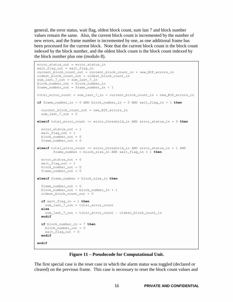
4.4.4 Computational Unit The bit-error rate monitoring circuitry was designed to keep the circuit size and complexity to a minimum. The largest mass of combinational logic is contained in the Computational unit. However, by using a time-slice architecture, we are able to share one instance of the large of logic to be used for all 16 possible lines. The Computational unit is shown in Figure 7, and is responsible for updating the register and alarm status values. The algorithm used to determine whether the bit-error count has exceeded the user-defined thresholds, and update the register values is outlined in Figure 11.
The computational block pseudocode begins by declaring the expected output values, followed by a decision structure, which determines if a special case must be handled. In
. PRIVATE AND CONFIDENTIAL 16
general, the error status, wait flag, oldest block count, sum last 7 and block number values remain the same. Also, the current block count is incremented by the number of new errors, and the frame number is incremented by one, as one additional frame has been processed for the current block. Note that the current block count is the block count indexed by the block number, and the oldest block count is the block count indexed by the block number plus one (modulo 8). error_status_out = error_status_in wait_flag_out = wait_flag_in current_block_count_out = current_block_count_in + new_BIP_errors_in oldest_block_count_out = oldest_block_count_in sum_last_7_out = sum_last_7_in block_number_out = block_number_in frame_number_out = frame_number_in + 1 total_error_count = sum_last_7_in + current_block_count_in + new_BIP_errors_in if frame_number_in = 0 AND block_number_in = 0 AND wait_flag_in = 1 then current_block_count_out = new_BIP_errors_in sum_last_7_out = 0 elseif total_error_count >= error_threshold_in AND error_status_in = 0 then error_status_out = 1 wait_flag_out = 1 block_number_out = 0 frame_number_out = 0 elseif total_error_count <= error_threshold_in AND error_status_in = 1 AND frame_number = block_size_in AND wait_flag_in = 1 then error_status_out = 0 wait_flag_out = 1 block_number_out = 0 frame_number_out = 0 elseif frame_number = block_size_in then frame_number_out = 0 block_number_out = block_number_in + 1 oldest_block_count_out = 0 if wait_flag_in = 1 then sum_last_7_out = total_error_count else sum_last_7_out = total_error_count – oldest_block_count_in endif if block_number_in = 7 then block_number_out = 0 wait_flag_out = 0 endif endif
Figure 11 – Pseudocode for Computational Unit.
The first special case is the reset case in which the alarm status was toggled (declared or cleared) on the previous frame. This case is necessary to reset the block count values and

. PRIVATE AND CONFIDENTIAL 17
to reset the start of the sliding window. It is necessary to reset the sliding window and discard old data since for the alarm clearing/declaring different sets of parameters are used and the window size might be different. To indicate that the full window of data is not yet valid, the wait flag is used to indicate that a full 8 monitoring blocks have not yet been processed since a change in alarm status.
The second case declares an alarm if the current BIP error total is greater than the error threshold parameter, and an alarm has not already been declared. The third case clears an alarm if the current BIP error total is less than the error threshold parameter, an alarm has already been declared and it has reached the end of a sliding window period. It is important to note that an alarm can be declared any time the error count exceeds the threshold. However, it can only be cleared at the end of a sliding window with eight valid monitoring blocks.
The final case determines if the block number pointer should advance to the next monitoring block. If the frame count has reached the monitoring block size, it will be reset to zero, and the monitoring block pointer will be advanced. At this point the sum_last_7 value is updated. Notice that if the wait flag is asserted, the oldest block count is ignored, as the data is invalid. Finally, as the block number pointer rolls over from the 7th monitoring block to monitoring block number zero, the wait flag is cleared regardless of its previous value, as all registers should contain valid values at this point.
Note that all variables with the suffix ‘_in’ are input parameters, and all variables with the suffix ‘_out’ are output parameters. Also, the current_block_count, as selected by the multiplexer circuitry, is equivalent to the kth block_count for a given set of registers, where k is the input block_number. Moreover, the oldest_block_count is the (k+1 modulo 8)th block count for a given register set.
5 Circuit Implementation The bit-error rate monitoring circuit was implemented using the hardware description language VHDL. VHDL allows for increased productivity and quality of design by eliminating irrelevant detail, allowing technology-independent description, catching errors earlier, and promoting portable and interoperable models from the gate to system level (Ashenden, 1996, vii). Using Electronic Design Automation (EDA) tools, the designer can compile and synthesize the VHDL description into a gate-level net-list. These tools save the designer from being overwhelmed by masses of detail when designing large Integrated Circuits (ICs)
For this thesis project, Cadence EDA tools were used for compilation, synthesis and simulation of the design. Due to good planning, the circuit implementation in VHDL was relatively painless, and after a few compilation attempts, all syntax errors were eliminated, and the design compiled successfully.
5.1 Synthesis The circuit was synthesized using a 50 ns timing constraint, and maximum optimization effort. This synthesis process creates a gate-level net-list, which implements all the functions of the high-level description, using as few logic gates as possible. The 50 ns timing constraint instructs the synthesis tool to create a net-list in such a manner that all

. PRIVATE AND CONFIDENTIAL 18
clocked flip-flop transitions happen within 50 ns of a clock edge. The timing constraint is extremely important since there might be gate configurations that reduce the number of gates, yet increase the flip-flop to flip-flop timing. By using the timing constraint, we can ensure that all flip-flop to flip-flop timing is met.
5.2 Power Consumption The final synthesized circuit had a total size of 39,965 gates for combinational logic, and 5,350 flip-flops. Using this information, and process specific information for fabrication, I was able to calculate the expected power consumption for the circuit. The average power consumption per gate is a function of the transistor capacitance, the voltage swing, and the frequency with which the gate switches. The power calculation parameters and results are shown in Table 7.
Table 7 – Power Calculation.
Count Power Dissipation Coefficient
Operating Frequency
Switching Probability Power
(mW/MHz/gate) (MHz) (0 → 0.5) (mW) Gates 39,965 3.120×10⁻⁴ 19.44 0.003 0.73 Flip-flops 5,350 1.764×10⁻³ 19.44 0.0001 0.04
The expected power consumption is calculated by multiplying the gate or flip-flop count by the respective power dissipation coefficient, operating frequency and switching probability. The power dissipation coefficient takes into account the gate capacitance and switching voltage for the process. The operating frequency is the frequency of the clock controlling the circuit. And, the switching probability is the probability that a gate will toggle on a clock edge. In our case, we only expect most flip-flops to be updated once a frame at most, and the probability of a bit switching is only one half. Similarly, we only expect the gates to be toggling during the first 32 clock cycles of a frame.
Overall, the circuit is expected to consume about three quarters of a milliwatt. This is well within the power consumption limit of 2 mW allotted for the circuit.
6 Circuit Testing Testing the circuit through simulations is a very important stage in the design process. With the high cost of fabricating multiple revisions of a large integrated circuit, it is important that the design work correctly on the first revision. Simulations were run using Cadence’s NCSIM tool to ensure correct functionality of the circuit.
The circuit was initially simulated on its own (circuit-level simulation) to ensure correct functionality and to allow for quick simulations. After ensuring that the circuit operated properly under a variety of conditions, it was simulated as part of the entire design (top-level simulation). Simulating the circuit as a stand-alone component allows for faster simulations, increasing the speed of testing. However, simulations of the circuit as part of the overall SONET Framer design are much more complex and slower. Nevertheless, these simulations are necessary in order to ensure correct connectivity.
. PRIVATE AND CONFIDENTIAL 19
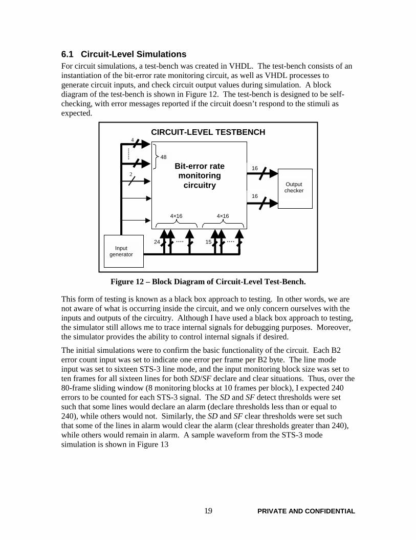
6.1 Circuit-Level Simulations For circuit simulations, a test-bench was created in VHDL. The test-bench consists of an instantiation of the bit-error rate monitoring circuit, as well as VHDL processes to generate circuit inputs, and check circuit output values during simulation. A block diagram of the test-bench is shown in Figure 12. The test-bench is designed to be self-checking, with error messages reported if the circuit doesn’t respond to the stimuli as expected.
48
Output checker
16
16
15 24
4×16 4×16
2 Bit-error rate monitoring
circuitry
4 CIRCUIT-LEVEL TESTBENCH
Input generator
Figure 12 – Block Diagram of Circuit-Level Test-Bench.
This form of testing is known as a black box approach to testing. In other words, we are not aware of what is occurring inside the circuit, and we only concern ourselves with the inputs and outputs of the circuitry. Although I have used a black box approach to testing, the simulator still allows me to trace internal signals for debugging purposes. Moreover, the simulator provides the ability to control internal signals if desired.
The initial simulations were to confirm the basic functionality of the circuit. Each B2 error count input was set to indicate one error per frame per B2 byte. The line mode input was set to sixteen STS-3 line mode, and the input monitoring block size was set to ten frames for all sixteen lines for both SD/SF declare and clear situations. Thus, over the 80-frame sliding window (8 monitoring blocks at 10 frames per block), I expected 240 errors to be counted for each STS-3 signal. The SD and SF detect thresholds were set such that some lines would declare an alarm (declare thresholds less than or equal to 240), while others would not. Similarly, the SD and SF clear thresholds were set such that some of the lines in alarm would clear the alarm (clear thresholds greater than 240), while others would remain in alarm. A sample waveform from the STS-3 mode simulation is shown in Figure 13
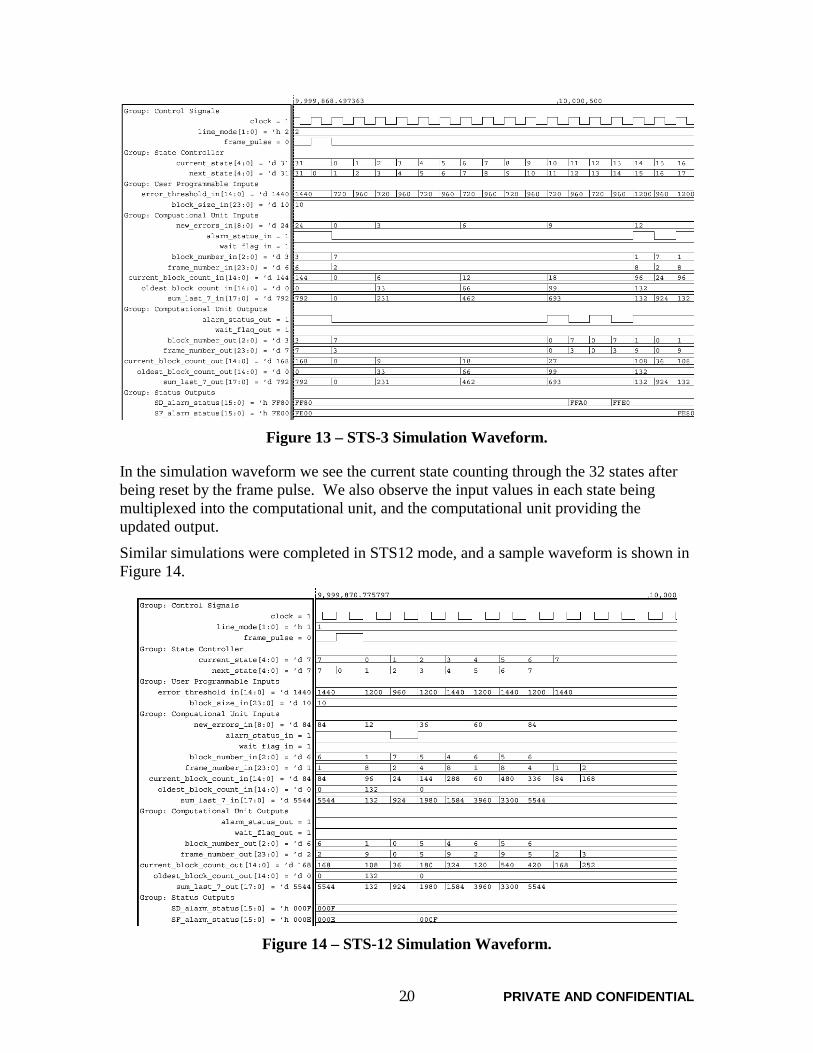
. PRIVATE AND CONFIDENTIAL 20
Figure 13 – STS-3 Simulation Waveform.
In the simulation waveform we see the current state counting through the 32 states after being reset by the frame pulse. We also observe the input values in each state being multiplexed into the computational unit, and the computational unit providing the updated output.
Similar simulations were completed in STS12 mode, and a sample waveform is shown in Figure 14.
Figure 14 – STS-12 Simulation Waveform.
. PRIVATE AND CONFIDENTIAL 21
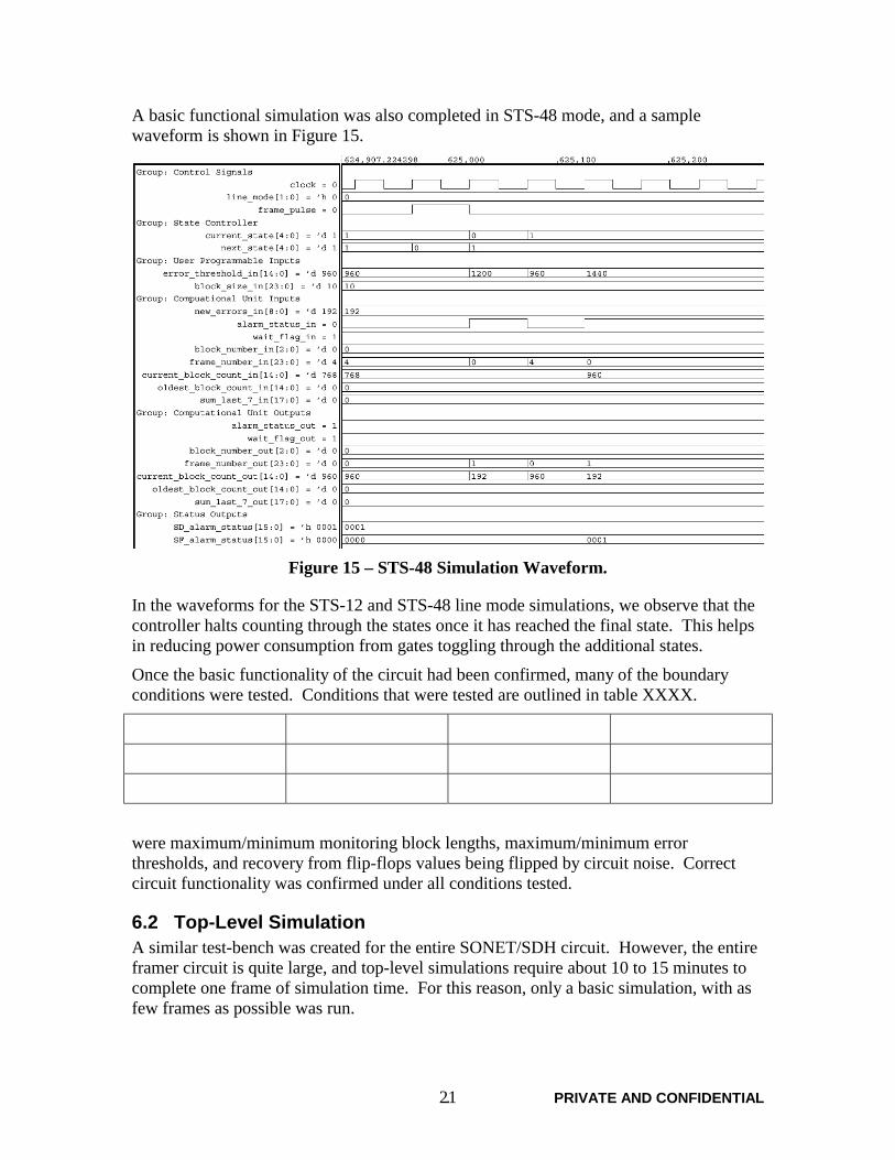
A basic functional simulation was also completed in STS-48 mode, and a sample waveform is shown in Figure 15.
Figure 15 – STS-48 Simulation Waveform.
In the waveforms for the STS-12 and STS-48 line mode simulations, we observe that the controller halts counting through the states once it has reached the final state. This helps in reducing power consumption from gates toggling through the additional states.
Once the basic functionality of the circuit had been confirmed, many of the boundary conditions were tested. Conditions that were tested are outlined in table XXXX.
were maximum/minimum monitoring block lengths, maximum/minimum error thresholds, and recovery from flip-flops values being flipped by circuit noise. Correct circuit functionality was confirmed under all conditions tested.
6.2 Top-Level Simulation A similar test-bench was created for the entire SONET/SDH circuit. However, the entire framer circuit is quite large, and top-level simulations require about 10 to 15 minutes to complete one frame of simulation time. For this reason, only a basic simulation, with as few frames as possible was run.

. PRIVATE AND CONFIDENTIAL 22
Also, for the top-level test-bench I do not have direct control over the BIP8 error-counts, instead, I must introduce actual SONET frames with the desired number of bit-errors into the device. A third-party tool was used to generate the SONET frames to ensure that they were compliant with the SONET standards. The SD/SF monitoring block size and error threshold values were programmed into the device using the microprocessor interface. The values were chosen to ensure that some lines would go into alarm state, while others did not, and that some of the lines in alarm would clear.
The top-level simulations indicated some problems in the connectivity of the bit-error rate monitoring circuit to the BIP-8 error counter circuitry. These problems were fixed and the circuit functioned correctly under the basic test condition in all three line modes.
7 Conclusion In high-speed networks, an important consideration is quality of service. Customers want a guaranteed level of data integrity. To provide data integrity, network traffic must be monitored in real-time to determine if there are any faults in the network. The bit error rate monitoring circuit, which I designed as my thesis project, will aid in the operation and maintenance of high-speed optical networks. Moreover, the design is user configurable to handle both SONET and SDH standards.
Through good design practices, I was able to create an efficient circuit implementation. The final gate count was reasonable, and the power consumption was well within the allotted power. The modern design process, making use of high-level hardware description language, is relatively fast and efficient. The number of design revisions can also be reduced by completely simulating a design before it is ever produced. Other tools allow us to minimize gate counts, ensure that timing constraints are met, and automate the place and route process.
As today’s circuit designs become larger and more complex, it is important to have tools that can cope with the larger scale of design. I have shown, through the design of a bit-error rate monitoring circuit, that with the right tools, it is becoming easier to design larger and more complex systems. However, it is also necessary to maintain a hierarchical approach towards design, as synthesizing and testing extremely large circuits remains slow and difficult.
Finally, this thesis project has helped me gain a better understanding of the overall circuit design, test, and implementation process. I have gained invaluable knowledge and experience that I can apply as a Product Design Engineer at West Bay Semiconductor.

. PRIVATE AND CONFIDENTIAL 23
References
Ashenden, Peter J., The Designer’s Guide to VHDL, Morgan Kaufman Publishers Inc., 1996.
Chow, Ming-Chwan, UNDERSTANDING SONET/SDH: Standards and Applications, Andan Publisher, 1995.
Goralski, Walter J., SONET: A Guide to Synchronous Optical Networks, McGraw Hill, New York, 1997.
GR-253-CORE, Synchronous Optical Network (SONET) Transport Systems: Common Generic Criteria, Issue 2, December 1995, Revision 2, Telcordia, January 1999.
Kartalopoulos, Stamatios V., Understanding SONET/SDH and ATM, IEEE Press, 1999
Papoulis, Athanasios, Probability, Random Variables, and Stochastic Processes, Second Edition, McGraw-Hill, New York, 1984.
T1.231-1997, Digital Hierarchy – Layer 1 In-Service Digital Transmission Performance Monitoring, ANSI, October 1997.