Embed Size (px)
Citation preview
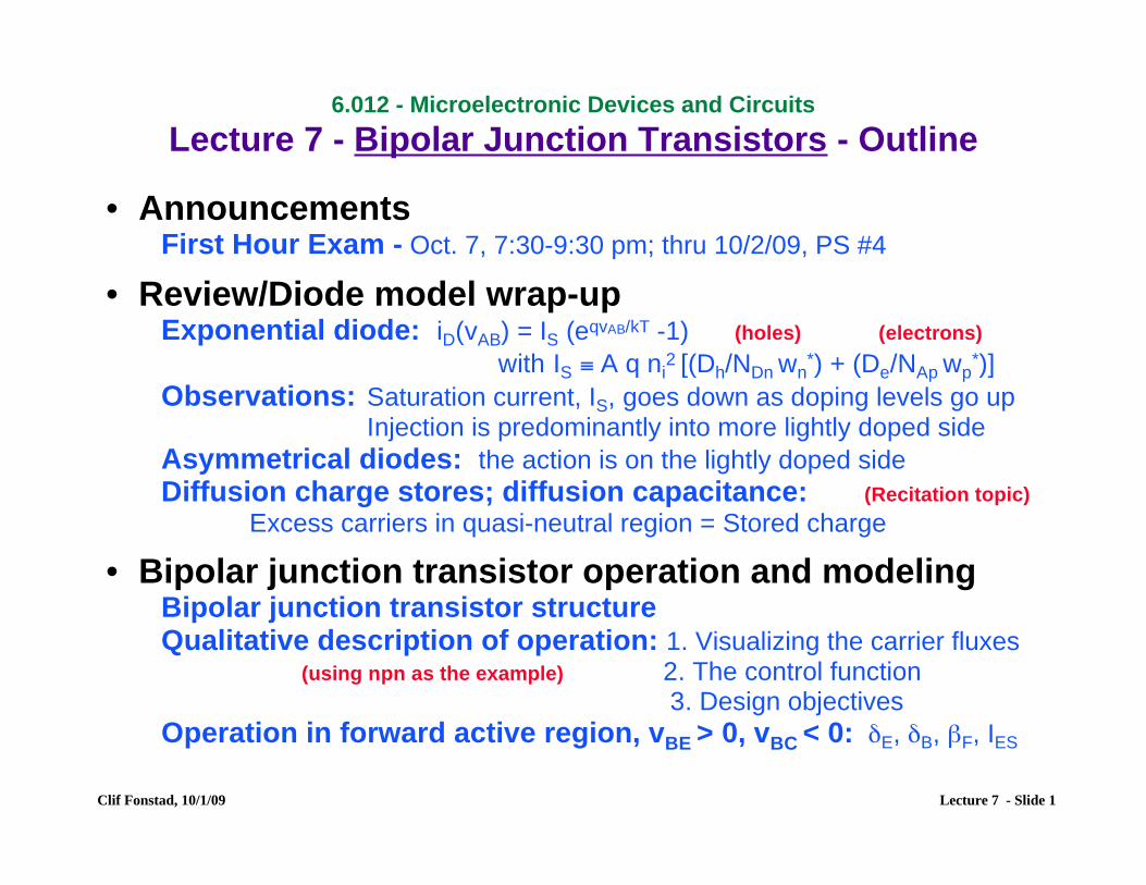
6.012 - Microelectronic Devices and Circuits Lecture 7 - Bipolar Junction Transistors - Outline
• Announcements First Hour Exam - Oct. 7, 7:30-9:30 pm; thru 10/2/09, PS #4
• Review/Diode model wrap-upExponential diode: iD(vAB) = IS (eqvAB/kT -1) (holes) (electrons)
with IS ≡ A q ni2 [(Dh/NDn wn
*) + (De/NAp wp*)]
Observations: Saturation current, IS, goes down as doping levels go up Injection is predominantly into more lightly doped side
Asymmetrical diodes: the action is on the lightly doped side Diffusion charge stores; diffusion capacitance: (Recitation topic)
Excess carriers in quasi-neutral region = Stored charge
• Bipolar junction transistor operation and modelingBipolar junction transistor structure Qualitative description of operation: 1. Visualizing the carrier fluxes
(using npn as the example) 2. The control function 3. Design objectives
Operation in forward active region, vBE > 0, vBC < 0: δE, δB, βF, IES
Clif Fonstad, 10/1/09 Lecture 7 - Slide 1
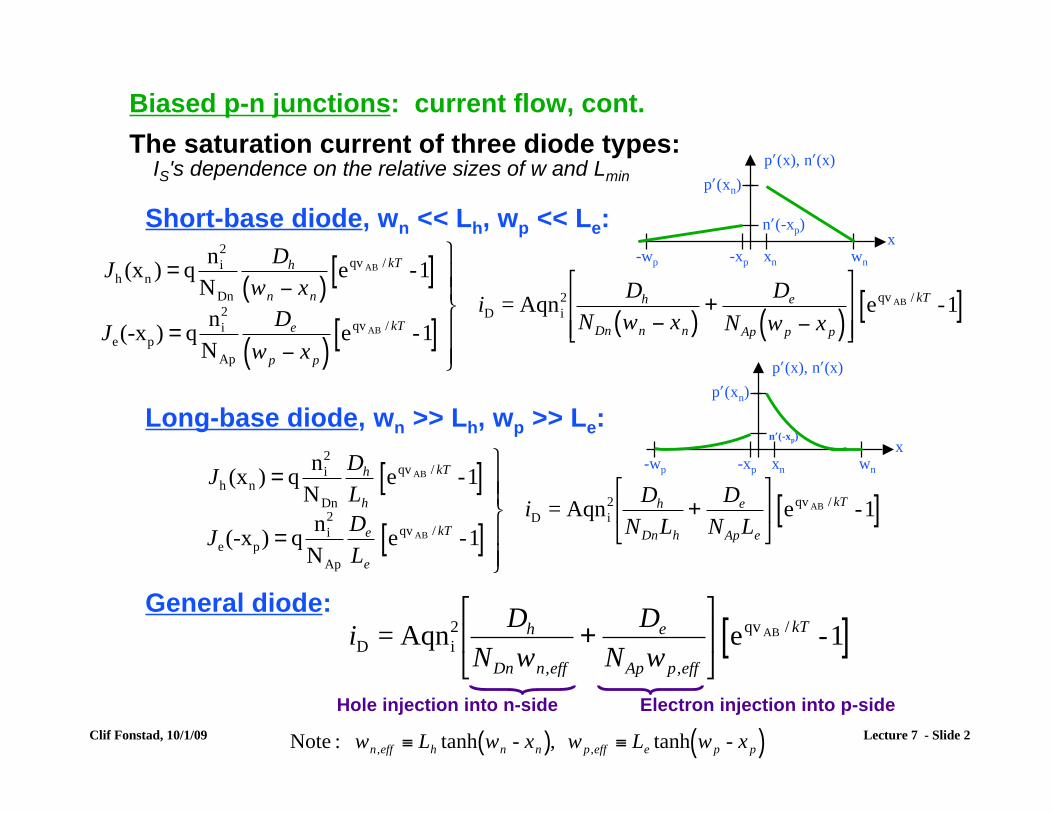
Biased p-n junctions: current flow, cont. The saturation current of three diode types:
!
iD = Aqni
2 Dh
NDnwn,eff
+De
NApwp,eff
"
# $
%
& ' eqv AB / kT -1[ ]
IS's dependence on the relative sizes of w and Lmin
Short-base diode, wn << Lh, wp << Le:
!
Jh (xn ) = qni
2
NDn
Dh
wn " xn( )eqv AB / kT -1[ ]
Je(-xp) = qni
2
NAp
De
wp " xp( )eqv AB / kT -1[ ]
#
$ % %
& % %
iD = Aqni
2 Dh
NDn wn " xn( )+
De
NAp wp " xp( )'
( ) )
*
+ , ,
eqv AB / kT -1[ ]
p’(x), n’(x)
x xn-xp-wp wn
n’(-xp)
p’(xn)
!
Jh (xn ) = qni
2
NDn
Dh
Lh
eqv AB / kT -1[ ]
Je(-xp) = qni
2
NAp
De
Le
eqv AB / kT -1[ ]
"
# $ $
% $ $
iD = Aqni
2 Dh
NDnLh
+De
NApLe
&
' (
)
* + eqv AB / kT -1[ ]
p’(x), n’(x)
x x-x-w npp wn
n’(-xp)
p’(xn)
Long-base diode, wn >> Lh, wp >> Le:
General diode:
Hole injection into n-side Electron injection into p-side Clif Fonstad, 10/1/09
!
Note : wn,eff " Lh tanh wn - xn( ), wp,eff " Le tanh wp - xp( ) Lecture 7 - Slide 2
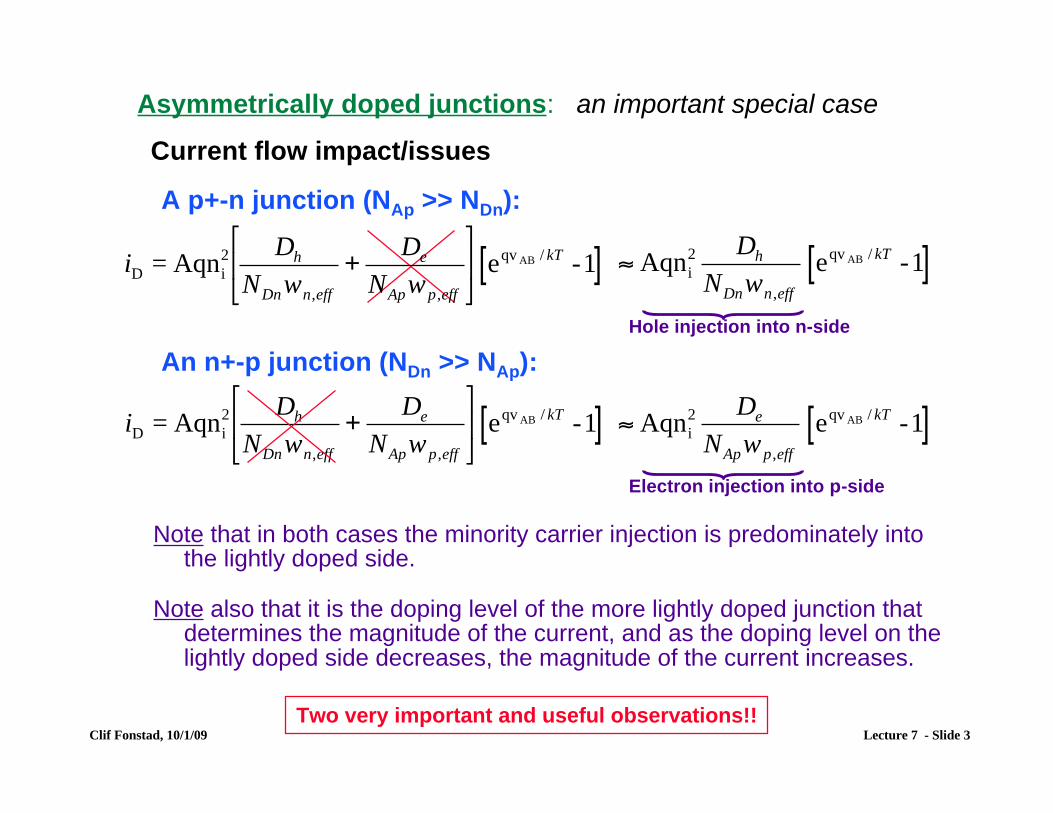
Asymmetrically doped junctions: an important special case
Current flow impact/issues
A p+-n junction (NAp >> NDn):
!
" Aqni
2 Dh
NDnwn,eff
eqv AB / kT -1[ ]
Hole injection into n-side
!
iD = Aqni
2 Dh
NDnwn,eff
+De
NApwp,eff
"
# $
%
& ' eqv AB / kT -1[ ]
An n+-p junction (NDn >> NAp):
Electron injection into p-side
!
iD = Aqni
2 Dh
NDnwn,eff
+De
NApwp,eff
"
# $
%
& ' eqv AB / kT -1[ ] ( Aqni
2 De
NApwp,eff
eqv AB / kT -1[ ]
Note that in both cases the minority carrier injection is predominately intothe lightly doped side.
Note also that it is the doping level of the more lightly doped junction thatdetermines the magnitude of the current, and as the doping level on thelightly doped side decreases, the magnitude of the current increases.
Two very important and useful observations!! Clif Fonstad, 10/1/09 Lecture 7 - Slide 3
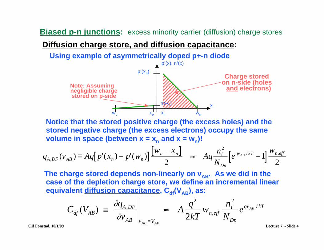
Biased p-n junctions: excess minority carrier (diffusion) charge stores
Diffusion charge store, and diffusion capacitance: Using example of asymmetrically doped p+-n diode
p’(x), n’(x)
p’(xn) Charge storedon n-side (holesNote: Assuming
negligible chargestored on p-side
n’(-xp) x -w -x
and electrons)
x wp p n n
Notice that the stored positive charge (the excess holes) and thestored negative charge (the excess electrons) occupy the same volume in space (between x = xn and x = wn)!
!
qA ,DF (vAB ) = Aq p'(xn ) " p'(wn )[ ]wn " xn[ ]
2# Aq
ni
2
NDn
eqvAB / kT
"1[ ]wn,eff
2
The charge stored depends non-linearly on vAB. As we did in the case of the depletion charge store, we define an incremental linear equivalent diffusion capacitance, Cdf(VAB), as:
Clif Fonstad, 10/1/09 Lecture 7 - Slide 4
!
Cdf (VAB) "#qA ,DF
#vAB vAB =VAB
$ Aq
2
2kTwn,eff
ni
2
NDn
eqvAB / kT
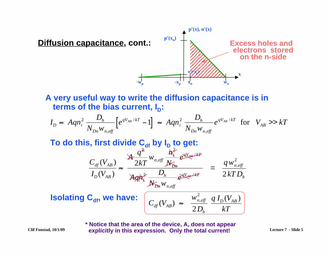
p’(x), n’(x)
p’(xn)Diffusion capacitance, cont.: Excess holes and
electrons stored on the n-side
n’(-xp) x -wp -xp xn wn
A very useful way to write the diffusion capacitance is interms of the bias current, ID:
!
ID " Aqni
2 Dh
NDnwn,eff
eqVAB / kT
#1[ ] " Aqni
2 Dh
NDnwn,eff
eqVAB / kT for VAB >> kT
To do this, first divide Cdf by ID to get:
!
Cdf (VAB )
ID (VAB )"
Aq
2
2kTwn,eff
ni
2
NDn
eqVAB / kT
Aqni
2 Dh
NDnwn,eff
eqVAB / kT
!
Cdf (VAB) "wn,eff
2
2Dh
q ID (VAB )
kT
Isolating Cdf, we have: !
=qwn,eff
2
2kT Dh
* Notice that the area of the device, A, does not appearClif Fonstad, 10/1/09 Lecture 7 - Slide 5explicitly in this expression. Only the total current!
d/2
-d/2
qA
qB( = -qA)
xn
-xp
qA
qB ( = -Q A)
-qNAp
qNDn
!
qAB ,DF (vAB ) " Aqni
2 Dh
NDnwn,eff
eqVAB / kT
#1[ ]
=wn,eff
2
2Dh
iD (vAB )
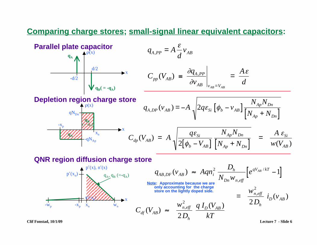
Comparing charge stores; small-signal linear equivalent capacitors:
Parallel plate capacitorρ(x)
x
!
qA ,PP = A"
dvAB
Cpp (VAB) #$qA ,PP
$vAB vAB =VAB
=A"
d
Depletion region charge store
!
qA ,DP (vAB ) = "A 2q#Si $b " vAB[ ]NApNDn
NAp + NDn[ ]
Cdp (VAB) = Aq#Si
2 $b "VAB[ ]NApNDn
NAp + NDn[ ]=
A #Si
w(VAB )
ρ(x)
x
QNR region diffusion charge store
Clif Fonstad, 10/1/09 Lecture 7 - Slide 6
qA, qB (=-qA) p’(x), n’(x)
x xn-xp-wp wn
n’(-xp)
p’(xn)
Note: Approximate because we areonly accounting for the chargestore on the lightly doped side.
!
Cdf (VAB) "wn,eff
2
2Dh
q ID (VAB )
kT
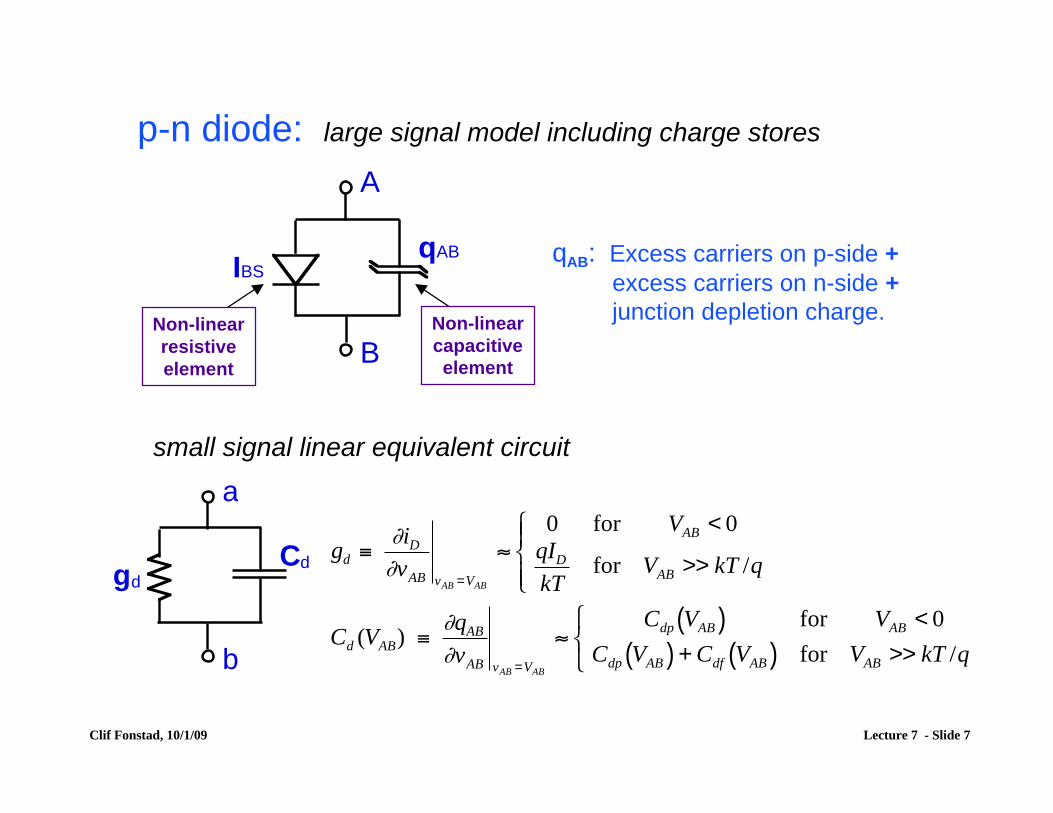
p-n diode: large signal model including charge stores
B
A
IBS
qAB
Non-linear resistive element
Non-linear capacitive element
qAB: Excess carriers on p-side + excess carriers on n-side + junction depletion charge.
small signal linear equivalent circuit
!
gd "#iD
#vAB vAB =VAB
$0 for VAB < 0
qID
kTfor VAB >> kT /q
% & '
( '
Cd (VAB) "#qAB
#vAB vAB =VAB
$Cdp VAB( ) for VAB < 0
Cdp VAB( ) + Cdf VAB( ) for VAB >> kT /q
% & ( b
a
gd
Cd
Clif Fonstad, 10/1/09 Lecture 7 - Slide 7
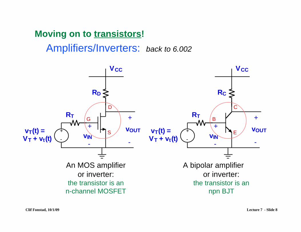
Moving on to transistors! Amplifiers/Inverters: back to 6.002
vT(t) =VT + vt(t)
VCC
vOUT
+
-vIN
+
-
+
-
RT
D
S
G
RD
vT(t) =VT + vt(t)
VCC
vOUT
+
-vIN
+
-
+
-
RT
C
E
B
RC
An MOS amplifier A bipolar amplifier or inverter: or inverter:
the transistor is an the transistor is an n-channel MOSFET npn BJT
Clif Fonstad, 10/1/09 Lecture 7 - Slide 8
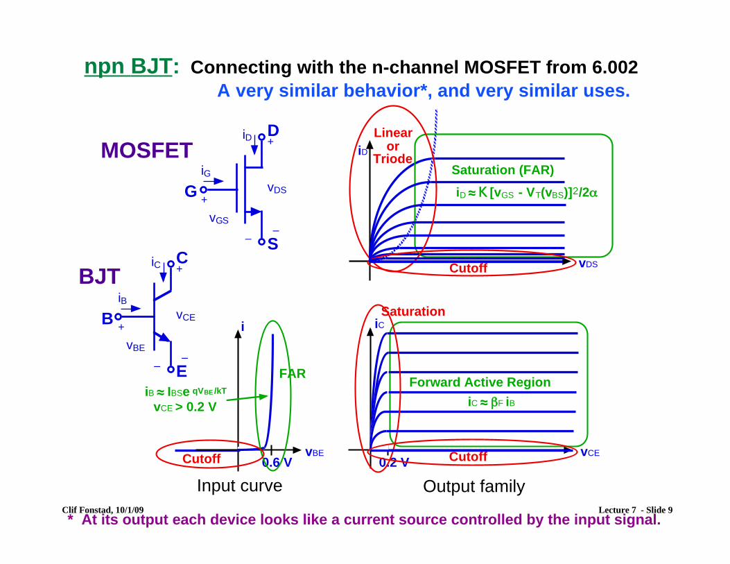
npn BJT: Connecting with the n-channel MOSFET from 6.002 A very similar behavior*, and very similar uses.
vDS
iD
Saturation (FAR)
Cutoff
Linearor
Triode
iD ! K [vGS - VT(vBS)]2/2!
iB
vBE vCE
iC
0.6 V 0.2 V
Forward Active RegionFAR
CutoffCutoff
Saturation
iC ! !F iBvCE > 0.2 ViB ! IBSe qVBE /kT
Input curve Output family
MOSFET
BJT
B
E
C
+
––
+
vBE
vCE
iB
iC
G
S
D
+
––
+
vGS
vDS
iG
iD
Clif Fonstad, 10/1/09 Lecture 7 - Slide 9* At its output each device looks like a current source controlled by the input signal.
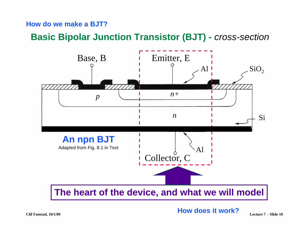
How do we make a BJT?
Basic Bipolar Junction Transistor (BJT) - cross-section
n+
n
p
Collector, C
Base, B Emitter, E
Al
Al
Si
SiO2
An npn BJTAdapted from Fig. 8.1 in Text
The heart of the device, and what we will model
How does it work?Clif Fonstad, 10/1/09 Lecture 7 - Slide 10
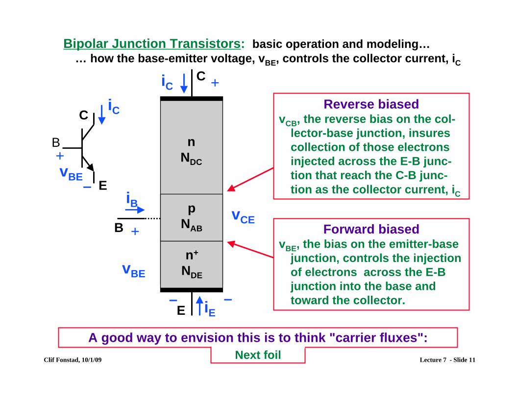
Bipolar Junction Transistors: basic operation and modeling… … how the base-emitter voltage, vBE, controls the collector current, iC
CiC
iCC
+
n
NDC
p
NAB
n+
NDE
Reverse biased vCB, the reverse bias on the col-
lector-base junction, insures collection of those electrons injected across the E-B junc-tion that reach the C-B junc-tion as the collector current, iC
B + vBE
− E iB
vCE B Forward biased
vBE, the bias on the emitter-base junction, controls the injection of electrons across the E-B junction into the base and toward the collector.
+
vBE
iE
−−E
Clif Fonstad, 10/1/09 Lecture 7 - Slide 11
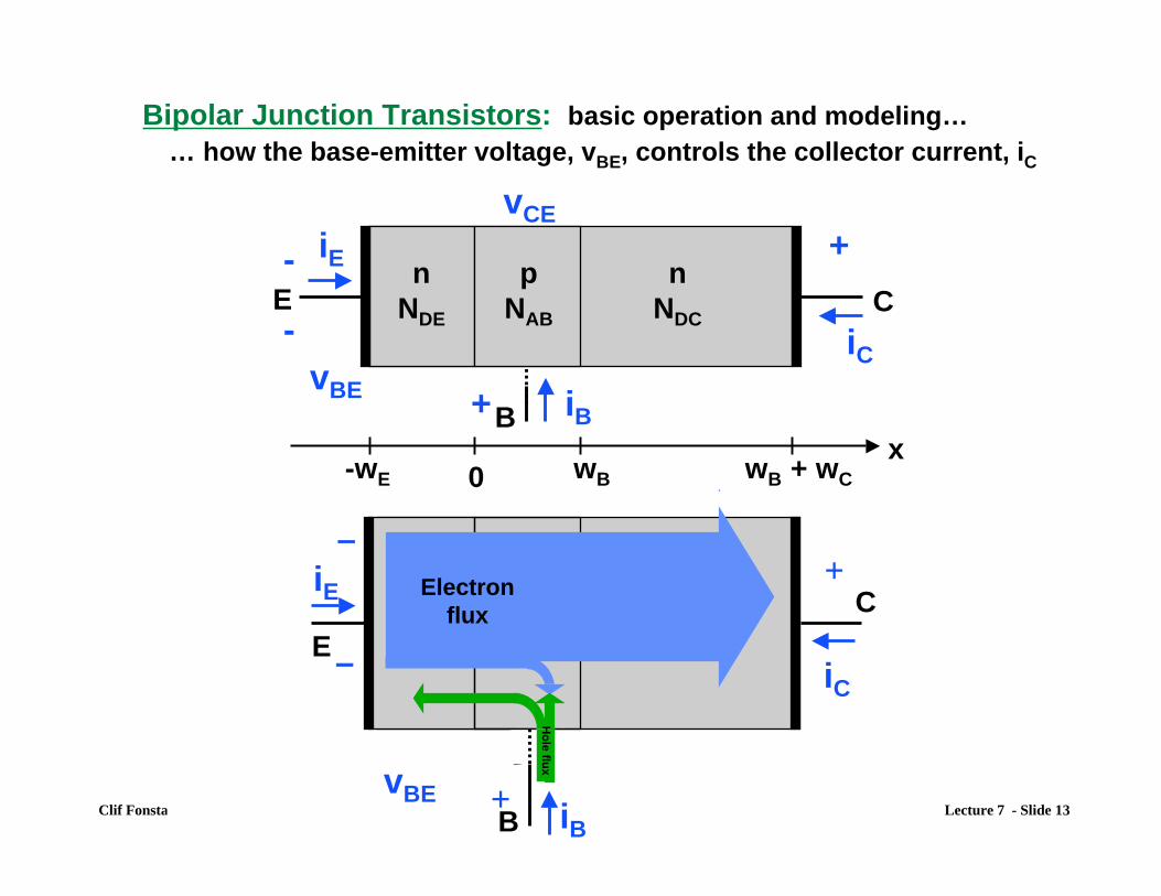
A good way to envision this is to think "carrier fluxes": Next foil
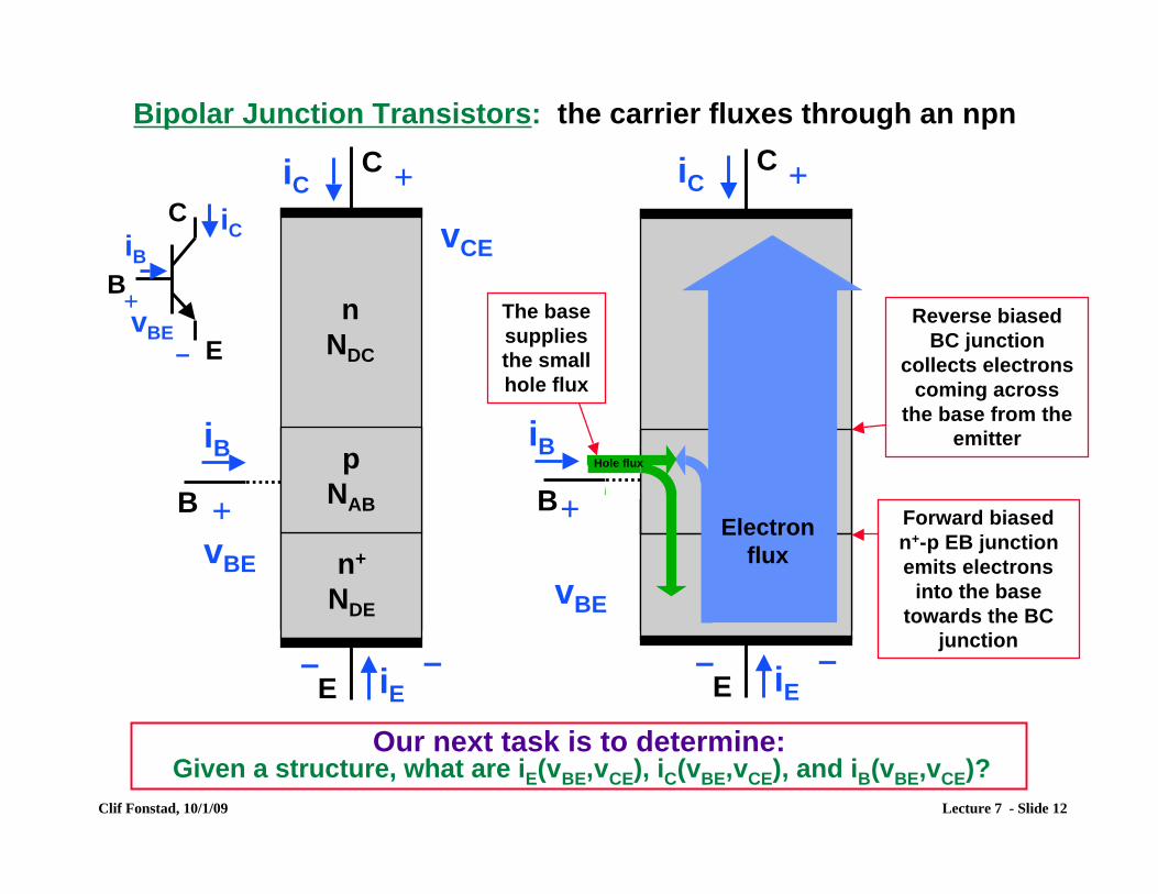
Bipolar Junction Transistors: the carrier fluxes through an npn
C CiC
C iC
+
The base supplies the small hole flux
Reverse biased BC junction
collects electrons coming across
the base from the emitter
+
+
E
B
−−
vBE
Electron
flux
Hole flux
into the base towards the BC
junction
iC
n
NDC
p
NAB
n+
NDE
vCE iB
B+ vBE
− E
iBiB
B Forward biased n+-p EB junction emits electrons
+
vBE
−−E iEiE
Our next task is to determine: Given a structure, what are iE(vBE,vCE), iC(vBE,vCE), and iB(vBE,vCE)?
Clif Fonstad, 10/1/09 Lecture 7 - Slide 12
d, 10/1/09
+
+
E
B
−
−
vBEiB
iC
iE Electron
fluxH
ole
flu
x
C
This is rigorous for vCB = 0, butalso very good when vCB > 0.
Bipolar Junction Transistors: basic operation and modeling… … how the base-emitter voltage, vBE, controls the collector current, iC
vCE +iE-
E C -
n p n NDE NAB NDC
iC vBE + iBB
x -wE wB + wC0 wB
Clif Fonsta Lecture 7 - Slide 13
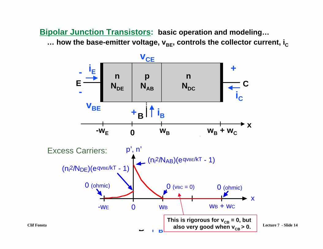
0-wE wB wB + wC
x
p!, n!
0 (vBC = 0) 0 (ohmic)0 (ohmic)
(ni2/NAB)(eqvBE/kT - 1)
(ni2/NDE)(eqvBE/kT - 1)
Excess Carriers:
+
+
E
B
−
−
vBE iB
iC
iE Electron
flux H
ole
flu
xC
d, 10/1/09 Clif Fonsta
+
+
E
−
−
vBEi
iC
iE Electron
fluxH
ole
flu
xC
+
+
E
B
−
−
vBEiB
iC
iE Electron
fluxH
ole
flu
x
C
Bipolar Junction Transistors: basic operation and modeling… … how the base-emitter voltage, vBE, controls the collector current, iC
vCE
n p n NDE NAB NDC
+iE-E C - iC
vBE + iBB x -wE wB + wC0 wB
Lecture 7 - Slide 14 B B
0-wE wB wB + wC
x
p!, n!
0 (vBC = 0) 0 (ohmic)0 (ohmic)
(ni2/NAB)(eqvBE/kT - 1)
(ni2/NDE)(eqvBE/kT - 1)
Excess Carriers:
This is rigorous for vCB = 0, but also very good when vCB > 0.
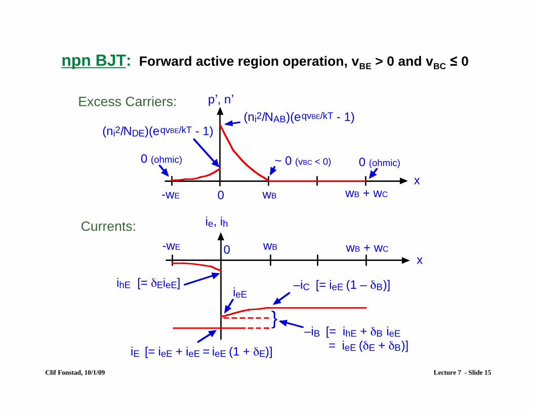
npn BJT: Forward active region operation, vBE > 0 and vBC ≤ 0
x0-wE wB wB + wC
ie, ih
ieE
ihE [= !EieE]
iE [= ieE + ieE = ieE (1 + !E)]
–iC [= ieE (1 – !B)]
}–iB [= ihE + !B ieE
= ieE (!E + !B)]
Currents:
0-wE wB wB + wC
x
p!, n!
~ 0 (vBC < 0) 0 (ohmic)0 (ohmic)
(ni2/NAB)(eqvBE/kT - 1)
(ni2/NDE)(eqvBE/kT - 1)
Excess Carriers:
Clif Fonstad, 10/1/09 Lecture 7 - Slide 15
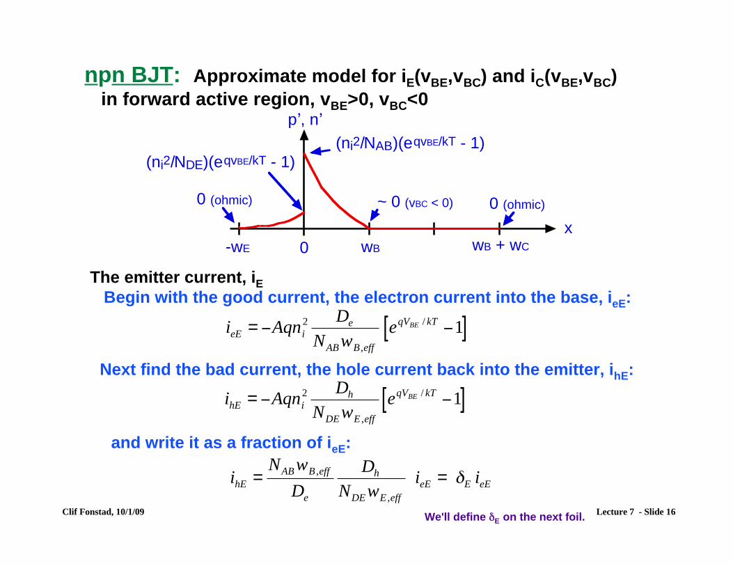
npn BJT: Approximate model for iE(vBE,vBC) and iC(vBE,vBC) in forward active region, vBE>0, vBC<0
0-wE wB wB + wC
x
p!, n!
~ 0 (vBC < 0) 0 (ohmic)0 (ohmic)
(ni2/NAB)(eqvBE/kT - 1)
(ni2/NDE)(eqvBE/kT - 1)
The emitter current, iE
Next find the bad current, the hole current back into the emitter, ihE:
Begin with the good current, the electron current into the base, ieE:
!
ieE = "Aqni
2 De
NABwB ,eff
eqVBE / kT
"1[ ]
!
ihE =NABwB ,eff
De
Dh
NDEwE ,eff
ieE = "E ieE
and write it as a fraction of ieE:
!
ihE = "Aqni
2 Dh
NDEwE ,eff
eqVBE / kT
"1[ ]
Clif Fonstad, 10/1/09 Lecture 7 - Slide 16 We'll define δE on the next foil.
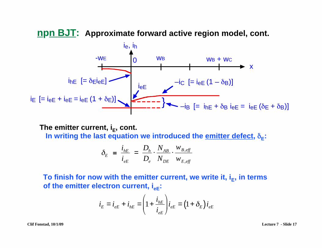
npn BJT: Approximate forward active region model, cont.
x0-wE wB wB + wC
ie, ih
ieE
ihE [= !EieE]
iE [= ieE + ieE = ieE (1 + !E)]
–iC [= ieE (1 – !B)]
}–iB [= ihE + !B ieE = ieE (!E + !B)]
The emitter current, iE, cont. In writing the last equation we introduced the emitter defect, δE:
!
"E #ihE
ieE
=Dh
De
$NAB
NDE
$wB ,eff
wE ,eff
To finish for now with the emitter current, we write it, iE, in terms of the emitter electron current, ieE:
!
iE = ieE + ihE = 1+ihE
ieE
"
# $
%
& ' ieE = 1+ (E( ) ieE
Clif Fonstad, 10/1/09 Lecture 7 - Slide 17
npn BJT: Approximate forward active region model, cont.
x0-wE wB wB + wC
ie, ih
ieE
ihE [= !EieE]
iE [= ieE + ieE = ieE (1 + !E)]
–iC [= ieE (1 – !B)]
}–iB [= ihE + !B ieE = ieE (!E + !B)]
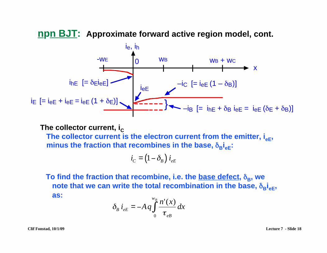
The collector current, iC The collector current is the electron current from the emitter, ieE, minus the fraction that recombines in the base, δBieE:
!
iC = 1"#B( ) ieE
To find the fraction that recombine, i.e. the base defect, δB, we note that we can write the total recombination in the base, δBieE, as:
!
"B ieE = #Aqn'(x)
$ eB
dx0
wB
%
Clif Fonstad, 10/1/09 Lecture 7 - Slide 18
npn BJT: Approximate forward active region model, cont.
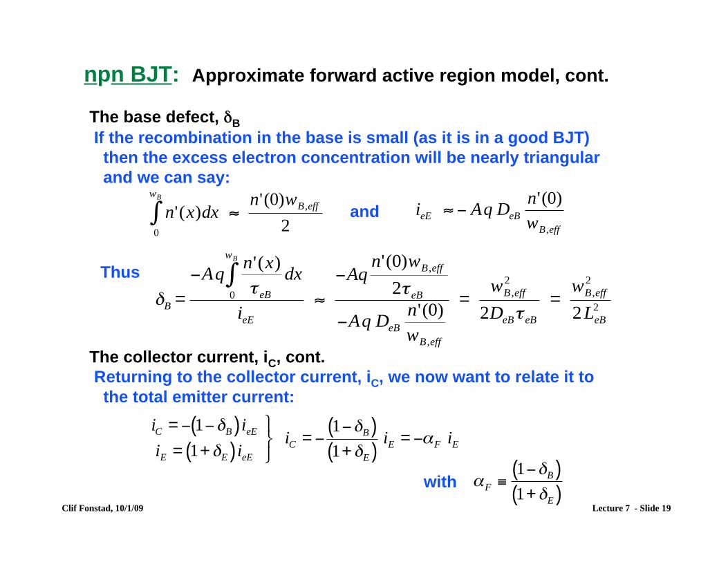
The base defect, δB If the recombination in the base is small (as it is in a good BJT)
then the excess electron concentration will be nearly triangular and we can say:
!
n'(x)dx0
wB
" #n'(0)wB ,eff
2and
!
ieE " # Aq DeB
n'(0)
wB ,eff
Thus
!
"B =#Aq
n'(x)
$ eB
dx0
wB
%
ieE
&
#Aqn'(0)wB ,eff
2$ eB
#Aq DeB
n'(0)
wB ,eff
=wB ,eff
2
2DeB$ eB
=wB ,eff
2
2LeB
2
The collector current, iC, cont. Returning to the collector current, iC, we now want to relate it to
the total emitter current:
Clif Fonstad, 10/1/09 Lecture 7 - Slide 19
!
iC = " 1"#B( ) ieE
iE = 1+ #E( ) ieE
$ % &
iC = "1"#B( )1+ #E( )
iE = "'F iE
!
"F#
1$%B( )
1+ %E( )
with
npn BJT: Approximate forward active region model, cont.
…and we have:
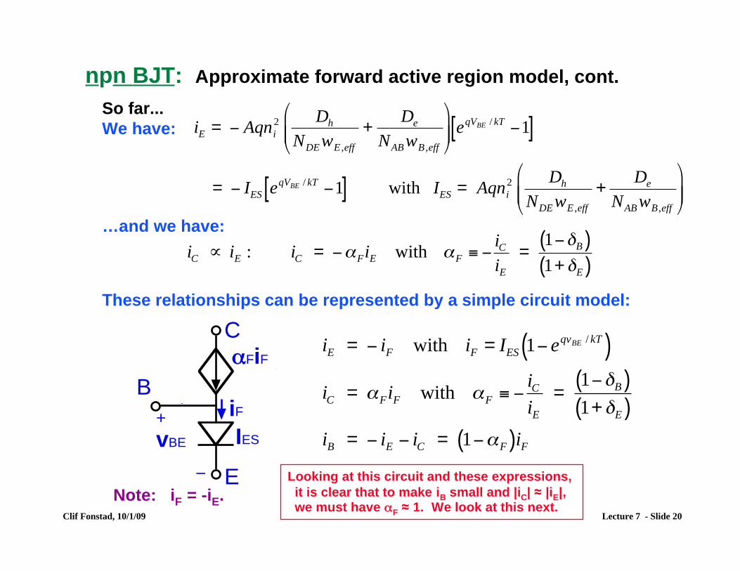
So far... We have:
!
iE = " Aqni
2 Dh
NDEwE ,eff
+De
NABwB ,eff
#
$ % %
&
' ( ( e
qVBE / kT "1[ ]
= " IES eqVBE / kT "1[ ] with IES = Aqni
2 Dh
NDEwE ,eff
+De
NABwB ,eff
#
$ % %
&
' ( (
!
iC " iE : iC = #$FiE with $F % #iC
iE=
1#&B( )1+ &E( )
These relationships can be represented by a simple circuit model:
Clif Fonstad, 10/1/09 Lecture 7 - Slide 20
B
E
C
vBE
+
–
iF
IES
!FiF
iB"FiB
or
Note: iF = -iE.
!
iE = " iF with iF = IES 1" eqvBE / kT( )
iC = #FiF with #F $ "iC
iE=
1"%B( )1+ %E( )
iB = " iE " iC = 1"#F( )iFLooking at this circuit and these expressions, it is clear that to make iB small and |iC| ≈ |iE|, we must have αF ≈ 1. We look at this next.
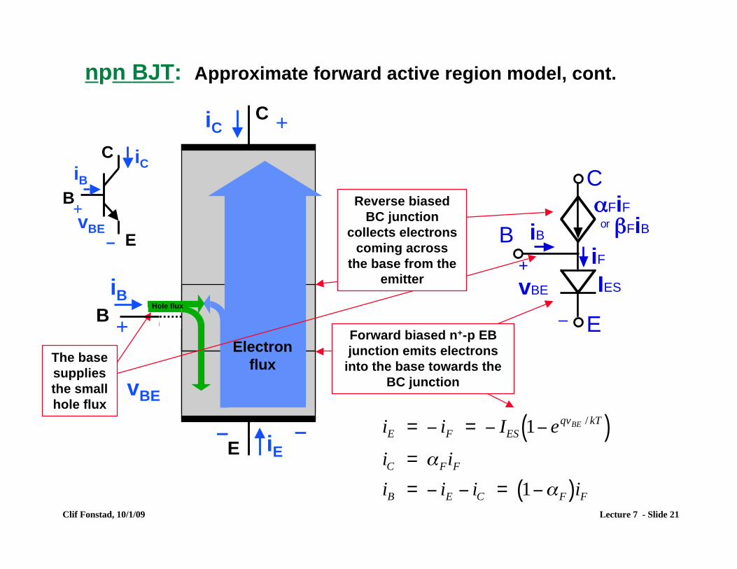
npn BJT: Approximate forward active region model, cont.
C
+ vBE
−
iCC
E
B
iB
The base supplies the small hole flux
+
+
E
B
−−
vBE
iB
iC
iE
Electron
flux
Hole flux
B
E
C
vBE
+
–
iF
IES
!FiF
iB"FiB
or
Reverse biased BC junction
collects electrons coming across
the base from the emitter
Forward biased n+-p EB junction emits electrons
into the base towards the BC junction
!
iE = " iF = " IES 1" eqvBE / kT( )
iC = #FiF
iB = " iE " iC = 1"#F( )iFClif Fonstad, 10/1/09 Lecture 7 - Slide 21
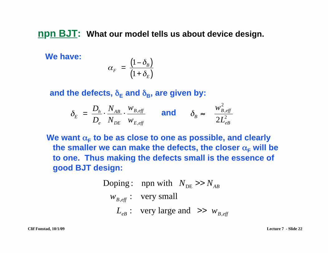
npn BJT: What our model tells us about device design.
We have:
!
"F
=1#$
B( )1+ $
E( )
and the defects, δE and δB, are given by:
!
"E =Dh
De
#NAB
NDE
#wB ,eff
wE ,eff
and
!
"B #wB ,eff
2
2LeB
2
We want αF to be as close to one as possible, and clearly the smaller we can make the defects, the closer αF will be to one. Thus making the defects small is the essence of good BJT design:
!
Doping : npn with NDE >> NAB
wB ,eff : very small
LeB : very large and >> wB ,eff
Clif Fonstad, 10/1/09 Lecture 7 - Slide 22
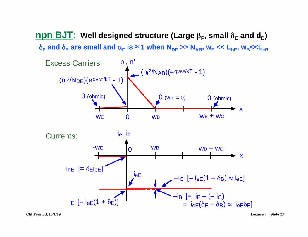
npn BJT: Well designed structure (Large βF, small δE and dB) δE and δB are small and αF is ≈ 1 when NDE >> NAB, wE << LhE, wB<<LeB
0-wE wB wB + wC
x
p!, n!
0 (vBC = 0) 0 (ohmic)0 (ohmic)
(ni2/NAB)(eqvBE/kT - 1)
(ni2/NDE)(eqvBE/kT - 1)
Excess Carriers:
x0-wE wB wB + wC
ie, ih
ieE
ihE [= !EieE]
iE [= ieE(1 + !E)]
–iC [= ieE(1 – !B) " ieE]
–iB [= iE – (– iC)
= ieE(!E + !B) " ieE!E]
Currents:
Clif Fonstad, 10/1/09 Lecture 7 - Slide 23
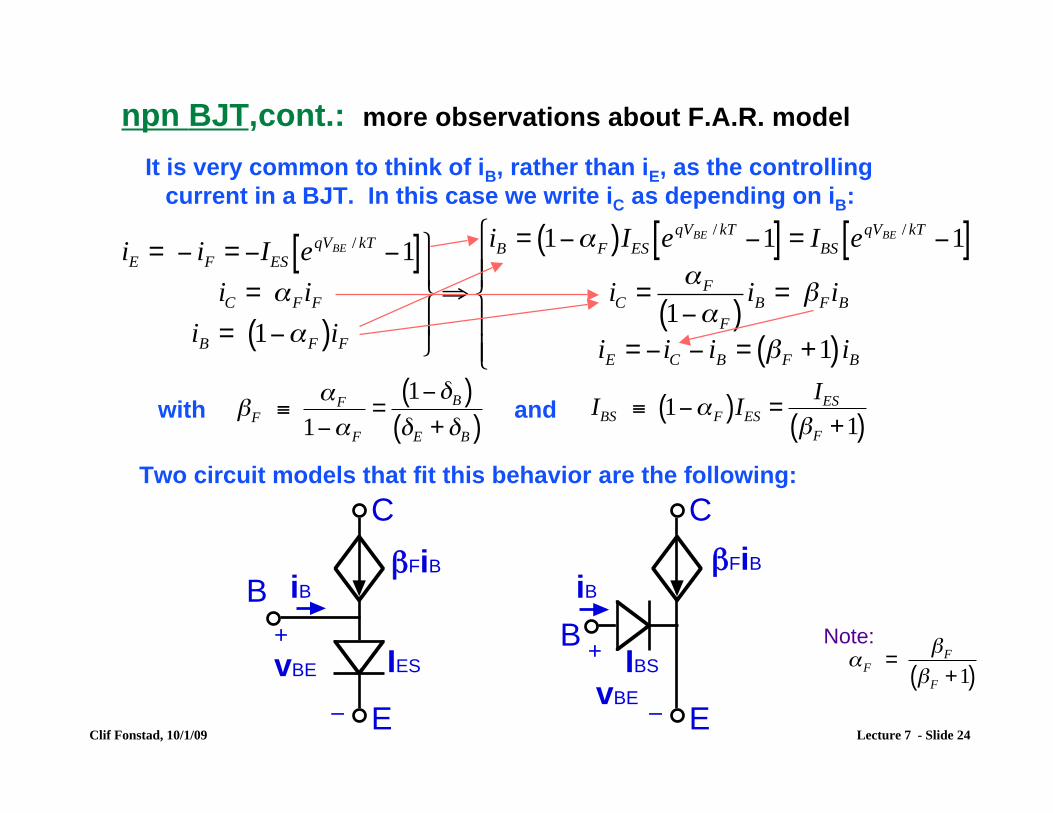
npn BJT,cont.: more observations about F.A.R. model
It is very common to think of iB, rather than iE, as the controlling current in a BJT. In this case we write iC as depending on iB:
!
"F#
$F
1%$F
=1%&
B( )&
E+ &
B( )
!
iE = " iF = "IES eqVBE / kT "1[ ]
iC = #FiF
iB = 1"#F( )iF
$
% &
' & (
iB = 1"#F( )IES eqVBE / kT "1[ ] = IBS e
qVBE / kT "1[ ]iC =
#F
1"#F( )iB = )FiB
iE = "iC " iB = )F +1( ) iB
*
+ & &
, & &
!
IBS " 1#$F( )IES =IES
%F +1( )andwith
Two circuit models that fit this behavior are the following:
Clif Fonstad, 10/1/09 Lecture 7 - Slide 24
!
"F
=#
F
#F
+1( )
B
E
C
vBE
+
–
IES
iB
!FiB
B
E
C
vBE
+
–
iB
IBS
!FiB
Note:
B
E
C
vBE
+
–
iB
IBS
!FiB
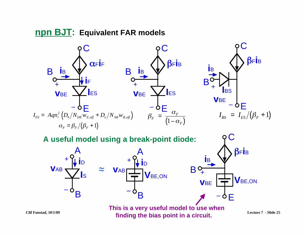
npn BJT: Equivalent FAR models
B
E
C
vBE
+
–
IES
iB
!FiB
B
E
C
vBE
+
–
iF
IES
!FiF
iBF
B
E
C
vBE
+
–
iB
VBE,ON
!FiBA
B
vAB
+
–
iD
IS
–
VBE,ON
A
B
vAB
+
–
iD
A useful model using a break-point diode:
≈
This is a very useful model to use when
!
"F
=#
F
1$#F( )
!
IBS = IES "F +1( )
!
IES = Aqni
2Dh NDEwE ,eff + De NABwB ,eff( )
"F = #F #F +1( )
Clif Fonstad, 10/1/09 Lecture 7 - Slide 25 finding the bias point in a circuit.
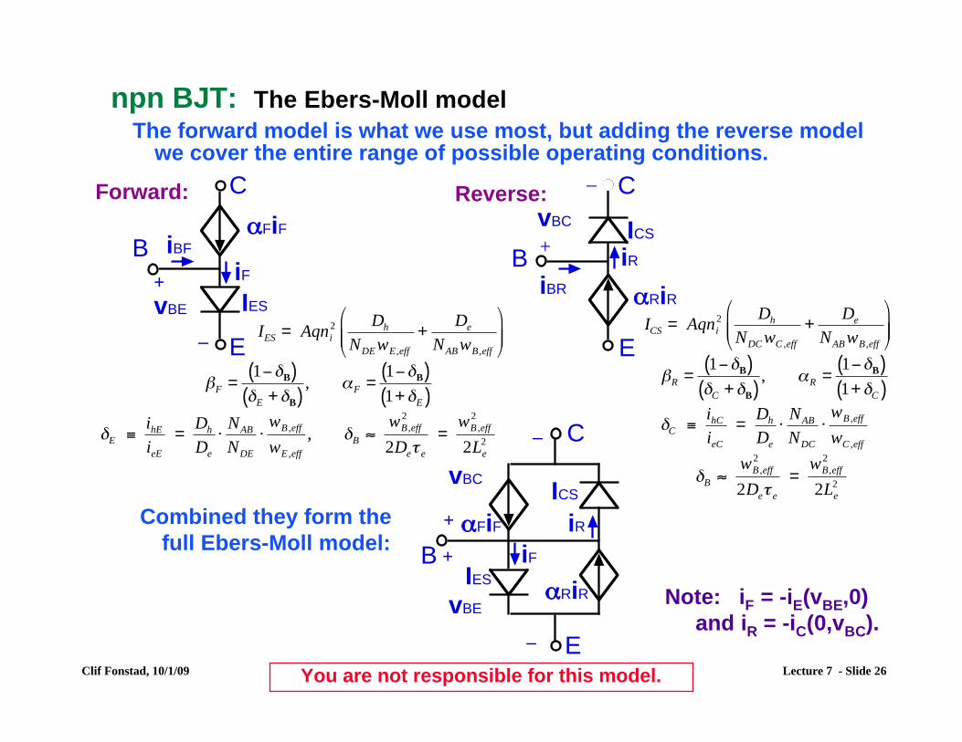
npn BJT: The Ebers-Moll model The forward model is what we use most, but adding the reverse model
we cover the entire range of possible operating conditions. CReverse: ICS
B
α RiR
!
ICS = Aqni
2 Dh
NDCwC ,eff
+De
NABwB ,eff
"
# $ $
%
& ' '
(R =1)*
B( )*C + *
B( ), +R =
1)*B( )
1+ *C( )
*C ,ihC
ieC
=Dh
De
-NAB
NDC
-wB ,eff
wC ,eff
*B .wB ,eff
2
2De/ e
=wB ,eff
2
2Le
2
E
Combined they form the full Ebers-Moll model:
Note: iF = -iE(vBE,0) and iR = -iC(0,vBC).
Clif Fonstad, 10/1/09
B
E
C
vBE
+
–
iF
IES
!FiF
iBF
vBC
iR
iBR
B
E
C
vBE
+
–
iF
IES
!FiF
vBC
+
–
iR
ICS
!RiR
Forward:
!
IES = Aqni
2 Dh
NDEwE ,eff
+De
NABwB ,eff
"
# $ $
%
& ' '
(F =1)*
B( )*E + *
B( ), +F =
1)*B( )
1+ *E( )
*E ,ihE
ieE
=Dh
De
-NAB
NDE
-wB ,eff
wE ,eff
, *B .wB ,eff
2
2De/ e
=wB ,eff
2
2Le
2
You are not responsible for this model. Lecture 7 - Slide 26
npn BJT: The Gummel-Poon model Another common model can be obtained from the Ebers-Moll model
is the Gummel-Poon model:
Reverse:
B
E
C
vBE
+
–
iBF
IS/!F
!FiBF
B
E
CvBC
+
–
iBR
IS/!R
!RiBRB
E
C
vBE
+
–
iF
IES
!FiF
iBF
Forward:
!
IS "#F
#F +1( )IES =
#R
#R +1( )ICS
= $FIES = $RICS
=
B
E
C
vBE
+
–
iBF
IS/!F
!FiBF - !RiBRiBR
IS/!R
+
–vBC
Combined they form the Gummel-Poon model:
• Aside from the historical interest, anothervalue this has for us in 6.012 is that it is an interesting exercise to show that the twoforward circuits above are equivalent.
Clif Fonstad, 10/1/09 You even less responsible for this model. Lecture 7 - Slide 27
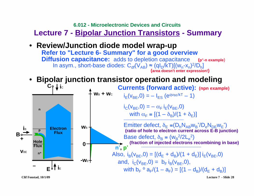
6.012 - Microelectronic Devices and Circuits
Lecture 7 - Bipolar Junction Transistors - Summary • Review/Junction diode model wrap-up
Refer to "Lecture 6- Summary" for a good overviewDiffusion capacitance: adds to depletion capacitance (p+-n example)
In asym., short-base diodes: Cdf(VAB) ≈ (qID/kT)[(wn-xn)2/Dh](area doesn't enter expression!)
iC
iE
iB
B
E
C
+
–
vBE
wB + wC
wB
-wE
n!, p!
ElectronFlux
HoleFlux
n
p
n+
0
• Bipolar junction transistor operation and modeling Currents (forward active): (npn example)
iE(vBE,0) = – IES (eqvBE/kT – 1)
iC(vBE,0) = – αF iE(vBE,0) with αF ≡ [(1 – δB)/(1 + δE)]
––––––––––––––––––––––––––––––––––––––––––
Emitter defect, δE ≡(DhNABwB*/DeNDEwE
*)(ratio of hole to electron current across E-B junction) Base defect, δB ≡ (wB
2/2Le2)
(fraction of injected electrons recombining in base) ––––––––––––––––––––––––––––––––––––––––––
Also, iB(vBE,0) = [(dE + dB)/(1 + dE)] iE(vBE,0) and, iC(vBE,0) = bF iB(vBE,0),
with bF º aF/(1 – aF) = [(1 – dB)/(dE + dB)] Clif Fonstad, 10/1/09 Lecture 7 - Slide 28
MIT OpenCourseWarehttp://ocw.mit.edu
6.012 Microelectronic Devices and Circuits Fall 2009
For information about citing these materials or our Terms of Use, visit: http://ocw.mit.edu/terms.