Embed Size (px)
Citation preview

BIOMEDICAL APPLICATIONS OF MEMS
Jack W. Judy University of California, Los Angeles 68-121 Engineering IV, Box 159410
Los Angeles, CA 90095-1594 Tel: (310) 206-1371
Abstract – Micromachining and MEMS technologies can be used to produce complex electrical, mechanical, fluidic, thermal, optical, and magnetic structures, devices, and systems on a scale ranging from organs to subcellular organelles. This miniaturization ability has enabled MEMS to be applied in many areas of biology, medicine, and biomedical engineering – a field generally referred to as BioMEMS. The future looks bright for BioMEMS to realize (1) microsensor arrays that act as an electronic nose or tongue, (2) microfabricated neural systems capable of controlling motor or sensory prosthetic devices, (3) painless microsurgical tools, and (4) complete microfluidic systems for total chemical or genetic analyses.
INTRODUCTION
Microelectromechanical systems (MEMS) is a technology of miniaturization that has been largely adopted from the integrated circuit (IC) industry and applied to the miniaturization of all systems (i.e., not only electrical systems but also mechanical, optical, fluidic, magnetic, etc). Miniaturization is accomplished with microfabrication processes, such as micromachining, that typically use lithography, although other non-lithographic precision microfabrication techniques exist (FIB, EDM, laser machining). Due to the enormous breadth and diversity of the field of MEMS, the acronym is not a particularly apt one. However, it is used almost universally to refer to the entire field (i.e., all devices produced by micromachining). Other names for this general field include “microsystems”, popular in Europe, and “micromachines”, popular in Asia.
For a discussion of the early work in MEMS, including many of the seminal papers, the interested reader is directed to reference [1]. For a comprehensive discussion of micromachining processes and MEMS devices, the interested reader is directed to the texts by Kovacs [2] and Madou [3].
MICROFABRICATION
Although many of the microfabrication techniques and materials used to produce MEMS have been borrowed from the IC industry, the field of MEMS has also driven the development and refinement of other microfabrication processes and non-traditional materials.
Conventional IC Processes and Materials:
- photolithography; thermal oxidation; dopant diffusion; ion implantation; LPCVD; PECVD; evaporation; sputtering; wet etching; plasma etching; reactive-ion etching; ion milling
- silicon; silicon dioxide; silicon nitride; aluminum
Additional Processes and Materials used in MEMS:
- anisotropic wet etching of single-crystal silicon; deep reactive-ion etching or DRIE; x-ray lithography; electroplating; low-stress LPCVD films; thick-film resist (SU-8); spin casting; micromolding; batch microassembly
- piezoelectric films such as PZT; magnetic films such as Ni, Fe, Co, and rare earth alloys; high temperature materials such as SiC and ceramics; mechanically robust aluminum alloys; stainless steel; platinum; gold; sheet glass; plastics such as PVC and PDMS

The methods used to integrate multiple patterned materials together to fabricate a completed MEMS device are just as important as the individual processes and materials themselves. The two most general methods of MEMS integration are described in the next two sub-sections: surface micromachining and bulk micromachining.
Surface Micromachining
Simply stated, surface micromachining is a method of producing MEMS by depositing, patterning, and etching a sequence of thin films, typically ~1 µm thick. One of the most important processing steps that is required of dynamic MEMS devices is the selective removal of an underlying film, referred to as a sacrificial layer, without attacking an overlaying film, referred to as the structural layer, used to create the mechanical parts. Figure 1 illustrates a typical surface micromachining process [4]. Surface micromachining has been used to produce a wide variety of MEMS devices for many different applications. In fact, some of them are produced commercially in large volumes (> million parts per month).
Substrate
Sacrificial LayerAnchor
Structural Layer
Release Etch
Substrate
Sacrificial LayerAnchor
Substrate
Sacrificial LayerAnchor
Structural LayerStructural Layer
Release EtchRelease Etch
Figure 1: Surface micromachining and the sacrificial layer technique.
Bulk Micromachining
Bulk micromachining differs from surface micromachining in that the substrate material, which is typically single-crystal silicon, is patterned and shaped to form an important functional component of the resulting device (i.e., the silicon substrate does not simply act as a rigid mechanical base as is
typically the case for surface micromachining). Exploiting the predictable anisotropic etching characteristics of single-crystal silicon, many high-precision complex 3-D shapes, such as V-grooves, channels, pyramidal pits, membranes, vias, and nozzles, can be formed [5]. An illustration of a typical bulk micromachining process is given in Figure 2.
{111 Planes}
Silicon Nitride Film
ThroughHole
Membrane V-Groove
(100) Silicon Waferp+ Silicon
{111 Planes}{111 Planes}
Silicon Nitride FilmSilicon Nitride Film
ThroughHole
Membrane V-GrooveThroughHole
Membrane V-Groove
(100) Silicon Waferp+ Silicon
(100) Silicon Waferp+ Silicon
Figure 2: Bulk micromachining.
Substrate Bonding
Silicon, glass, metal and polymeric substrates can be bonded together through a variety of processes (i.e., fusion bonding, anodic bonding, eutectic bonding, and adhesive bonding). Typically at least one of the bonded substrates has been previously micromachined. Substrate bonding is typically done to achieve a structure that is difficult to form otherwise (i.e., large cavities that may be hermetically sealed or a complex system of enclosed channels) or simply to add mechanical support and protection [2].
Non-Silicon Microfabrication
The development of MEMS has contributed significantly to the improvement of non-silicon microfabrication techniques. Two prominent examples are LIGA and plastic molding from micromachined substrates.

LIGA
LIGA is a German acronym standing for lithographie, galvanoformung (plating), and abformung (molding) [6]. However, in practice LIGA essentially stands for a process that combines extremely thick-film resists (often >1 mm) and x-ray lithography, which can pattern thick resists with high fidelity and results in vertical sidewalls. Although some applications may require only the tall patterned resist structures themselves, other applications benefit from using the thick resist structures as plating molds (i.e., material can be quickly deposited into the mold by electroplating). A drawback to LIGA is the need for high-energy x-ray sources (e.g., synchrotrons or linear accelerators) that are very expensive and rare (i.e., only several such sources exist in the U.S.).
SU-8
Recently a cheap alternative to LIGA, with nearly the same performance, has been developed. The solution is to use a special epoxy-resin-based optical resist, called SU-8, that can be spun on in thick layers (>500 µm), patterned with commonly available contract lithography tools, and yet still achieves vertical sidewalls [7].
Plastic Molding with PDMS
Polydimethylsiloxane (PDMS) is a transparent elastomer that can be poured over a mold (e.g., a wafer with a pattern of tall SU-8 structures), polymerized, and then removed simply by peeling it off of the mold substrate [8]. The advantages of this process include (1) many inexpensive PDMS parts can be fabricated from a single mold, (2) the PDMS will faithfully reproduce even sub-micron features in the mold, (3) PDMS is biocompatible and thus can be used in a variety of BioMEMS applications, and (4) since PDMS is transparent, tissues, cells, and other materials can be easily imaged through it. Common uses of PDMS in biomedical applications include: microstamping of biological compounds (to observe geometric behavior of cells and tissues) and microfluidics systems [9][8].
BIOMEDICAL MICROSENSORS
The majority of MEMS used in biomedical applications act as sensors. Examples include critical sensors used during surgery (i.e., measuring intravascular blood pressure), long-term sensors for prosthetic devices, and highly sophisticated sensor arrays for rapid lab-quality diagnosis at home. A
comprehensive discussion of all the different sensors and their applications is beyond the scope of this paper. Instead, a discussion of several classes of microsensors and an overview of their applications will be given.
Microsensors for Biomechanics
Studies of the forces created by and imposed on the body benefit from increasing the sensitivity of mechanical stress and strain sensors while also reducing their size and cost. The following are examples of microsensors used to study biomechanics.
Strain Gauges
Strain gauges are used to characterize the forces in the body. Since silicon is known to be an excellent piezoresistive material (i.e., it’s resistance changes as a function of applied force), it can be easily micromachined to form sub-millimeter multi-axis strain gauges [10]. Applications of such miniaturized strain gauges include orthopedic research and the study of muscles. Although the understanding of muscle function and structure is well understood at the whole-muscle and cellular levels, muscles have not been well characterized in the region in between. An improved understanding at this level would allow for the development of improved locomotion therapies and prosthetic devices.
Accelerometers
One class of microsensors that MEMS technology has had the most positive impact on are inertial sensors (i.e., accelerometers and gyros). Since inertial devices typically consist of a proof mass, mechanical flexure, and displacement sensor, MEMS technology is well suited to integrate each of these sensor elements into a single chip. In fact, it is also possible to integrate ICs with the micro-mechanical elements to add signal amplification and filtration capability to the chip-scale sensor [11]. Inertial microsensors are useful to determine impact level and patient posture.
Microsensors for Pneumatic Biosystems
Since much of the human body is a complex system of pumps, valves, vessels, and interconnects, pressure in many parts of the body is an important parameter to indicate the health and well being of a patient. Pressure sensors are used in medicine in many applications: blood pressure, bladder pressure,

and cerebral spinal fluid pressure to name a few. In addition to performance requirements, the size of pressure sensors, particularly those inserted into the body must be small and ideally disposable. MEMS technology is well positioned to deliver solutions to this opportunity. In fact, a good example is the commercially successful low-cost disposable medical pressure sensor developed by Lucas NovaSensor NPC-107 (Figure 3) [12]. In it a silicon micromachined sensing element is used to meet or exceed all industry requirements (e.g., sensitivity within +/-1% and linearity better than 1%). Another micromachined silicon pressure sensor produced by NovaSensor is made small enough (1 mm x 0.7 mm x 0.175 mm thick) to be inserted into a catheter and inserted into arteries.
Figure 4: Micromachined pressure sensor die with smallest having dimensions (175×700×1000 µm3).
Microsensors for Chemical Biosystems
Since living organisms are extremely sophisticated chemical processing systems, there are many biomedical applications for chemical sensors (e.g., medical diagnostic instruments, drug screening, implantable sensors for prostheses, and environment monitoring). Although the micromachining of chemical sensors is typically simple, other components sometimes used in a complete chemical sensor system (i.e., sample preparation and delivery, reaction control, and waste disposal) are more difficult to integrate together.
Impedance Sensors
The conductivity of some materials is affected by the presence and relative concentration of certain gases or vapors. Examples of these materials include
polymers doped with conductive particles, conductive polymers, and some metal oxides. The challenges common to impedance-based chemical sensors include identifying single gases, quantifying gas concentration, dealing with gas mixtures, sensitivity to water vapor, sensitivity to temperature changes, and microfabrication of arrays of uniquely sensitive sensors.
Polymer-Based Gas Sensors
Many polymers will geometrically swell reversibly when exposed to certain gases. Conductive polymers, such as polypyrrole, can be used directly as a viable chemiresistor. To use insulating polymers, they are doped with conductive particles to reduce their impedance (e.g., carbon black). When doped, the overall resistance of the doped polymer will change as a function of the chemically specific and concentration-dependent swelling [13]. One difficulty is that the polymers will swell to a greater or lesser extent when exposed to a variety of gases. To identify specific gases, the response pattern of many different polymers is needed. In addition to resistive measurements of geometric swelling, configurations that capacitively detect swelling have also been used. In these sensors the insulating polymers are not doped. Since it is known that certain diseases cause the body to generate specific gases that are not normally present, gas sensors have been used to help diagnose patient health.
In order to microfabricate arrays of sensors with unique polymers, the integration process must contend with the large volume of solvent that is typically present during polymer deposition. Furthermore, the microfabrication technique must not damage previously deposited polymers. One strategy is to use a removable mask to selectively deposit each polymer into a specific area. This technique has difficulty forming sub-millimeter sensors due to poor adhesion to the substrate when the mask is removed (i.e., the polymers adhere more strongly to the mask than to the substrate). Another strategy is to use a permanent microwell structure to contain the polymer-solvent solution in a well-defined sub-millimeter area without disturbing previously deposited polymers. An example of a polymeric impedance-based gas sensor that uses an SU-8 microwell structure is given in Figure 5.
Metal Oxides
The conductivity of certain metal oxides, most commonly SnO2, is known to vary as a function of the concentration of specific gasses (e.g., O2, H2,

CO, CO2, NO2, and H2S) when the metal oxide is heated sufficiently to induce a chemical reaction that is detected. There are several mechanisms that cause the resistance of the metal oxide to vary [2]. The microfabrication of these sensors can be relatively straightforward, unless additional micromachined features are added to improve sensor response and power consumption (i.e., integrating microfabricated heaters, thermal isolation structures (e.g., membranes) that require far less power to heat, and CMOS signal detection, amplification, and filtering circuitry.
Figure 5: Microfabricated polymer carbon-black gas sensor with SU-8 microwell for solvent containment (from [14]).
Electrochemical Sensors
The oxidation and reduction of chemical species on a conducting electrode can be observed by measuring the movement of charge. There are two primary methods of sensing electrochemical reactions: potentiometric and amperometric. Potentiometric sensors can be used to measure the equilibrium potential established between the electrode material and the solution, a potential that is dependent on the chemistry involved. Amperometric sensors measure the current generated by a reaction and thus give a measure of reaction rates. By controlling the potential of the electrode relative to the solution and measuring the charge flow induced, the presence of specific ions can be determined by observing the potential at which they undergo oxidation or reduction. This is a process known as voltammetry.
Micromachining processes can be used to accurately and reliable define the area, number, and relative position of electrodes that are exposed to
solution. In addition, the simple construction of a typical electrochemical sensor (i.e., a partially insulated metal trace on a substrate) allows ICs to be easily integrated with the electrode. The ICs can be used to provide on-chip signal processing and amplification.
Molecular-Specific Sensors
Chemical sensors that respond only to certain ions or molecules can be extremely selective. Among the most selective are the interactions between complex organic molecules, such as antigens and antibodies. One caveat is that often very selective sensors are also less reversible and thus may require special packaging to protect the sensors until they are needed. A prominent example of a molecularly sensitive amperometric sensor is one that uses a glucose oxidase enzyme to detect glucose. The enzyme, which is typically immobilized on or near electrodes, reacts with glucose and alters the local pH, oxygen concentration, and hydrogen peroxide concentration – events that can be electrochemically detected.
ISFETs
Field effect transistors (FETs) are very sensitive to variations in the amount of charge on their controlling electrodes (i.e., gate). If an ionic solution acts as the gate of a FET, the device will be tremendously sensitive to the overall ion concentration of the solution (i.e., not selective to specific ions). A good pH sensor can be made this way and indeed one exists [15]. By coating the gate of the FET with a compound that will selectively bind or allow to pass only specific ions or molecules, an ion-sensitive FET, or ISFET, can be realized. Common difficulties with ISFETs, as with all chemical sensors, are drift and repeatability.
Resonant Sensors
The resonant frequency of a mechanical element is strongly dependent on its geometry, mechanical properties, and mass. By coating a resonating mechanical element, such as a beam or membrane, with a compound that will selectively bind to only specific ions or molecules, the mass of the mechanical element will increase with their concentration. The ion-concentration dependent mass loading can be determined by measuring the corresponding shift in the resonant frequency.

The most common resonant chemical sensors use acoustic waves driven along surfaces of a solid (i.e., surface acoustic waves, SAW) or in a thin membrane (i.e., flexural plate waves, FPW) [2],[16]. Acoustic-wave sensors have been used to detect liquid density, viscosity, specific gas vapors. Design challenges include (1) temperature sensitivity of the mechanical flexure, (2) selectivity of the binding compound, and (3) reversibility of the binding and mass loading process. MEMS technology impacts resonant chemical gas sensors by allowing miniature sensors to be produced at low cost.
Cell-Based Sensors
An innovative microsensor uses a cell as the primary transduction mechanism. An advantage of using cells to detect chemicals is that cells are microscopic chemical laboratories that can amplify a chemical signal (i.e., the detection a few molecules can lead to the production of many so called “second messanger” molecules) – essentially biological gain [17]. The amplified cell signal can be monitored by either detecting a chemical change within the cell or inferring the change by monitoring other parameters, such the electrical activity. One sensor uses chick myocardial cells to detect the presence of epinephrine, verapamil, and tetrodotoxin in the cell environment (Figure 6) [18]. Limitations of cell-based sensors include the lifetime and robustness of the cells.
Figure 6: Cell-based biosensor with microelectrode array [18].
Microsensors for Electrical Biosystems
The central and peripheral nervous systems are the primary electrical biosystems of interest. Many sensors and probes have been used to measure the electrical signals generated by neural tissue. Example include electrocardiogram (ECG), electroencephalogram (EEG), electroneurogram (ENG), electromyogram (EMG), and electroretino-
gram (ERG). These bioelectrical signals are typically transduced with either external or internal electrodes. With MEMS technology, many electrodes can be co-fabricated onto a single substrate so that both precise temporal and spatial information can be obtained. MEMS technology can also be used to shape the substrate into either arrays of microprobes capable of penetrating neural tissue (Figure 7) [19][21] or into a perforated membrane through which regenerating neural tissue can grow and then be monitored [20]. In the U.S. the University of Michigan [22], Stanford University [23], and the University of Utah [24] have spent years developing and improving various MEMS-based neural-electronic interfaces.
Figure 7: Microfabricated silicon neural probe arrays. Top: Close-up of the probes and electrodes [19].
The implications of MEMS technologies for neuroscience are revolutionary. We now have the potential to develop arrays of microsystems, which can be tailored to the physical and temporal dimensions of individual cells. Neuroscientists can now realistically envision sensing devices that allow real-time measurements at the cellular level. Information from such sensors could be monitored, analyzed, and used as a basis of experimental or medical intervention, again at a cellular level. Another example is the use of micromachined neural sensors and stimulators to control prosthetic limbs with processed signals recorded from the brain or spinal column.

BIOMEDICAL MICROACTUATORS
Microactuators are useful in biomedical applications when biological objects or their environment need to be controlled on the microscopic scale. Furthermore, the ability to integrate many microactuators as easily as only one makes it feasible to produce complex microsystems capable of controlling many parameters.
Micromanipulators
To manipulate cells, tissues, and other biological objects, micromanipulators must be driven by a microactuation mechanism capable of operating in a conductive solution. Good candidates include magnetic, pneumatic, thermal, and shape-memory alloy actuation. The magnetic microactuator shown in Figure 8 has been used to manipulate single-cell protozoa in saline [25]. The shape memory alloy microactuator shown in Figure 9 is capable of grasping tissues during endoscopic surgical procedures [26]. A second-generation device constructed with polymers is being commercialized by Micrus, Inc. and is presently in human trials.
Figure 8: Magnetic microactuator manipulating a single-cell protozoa (from [25]).
Figure 9: Surgical microgripper actuated by shape-memory-alloy forces (from [26]).
Surgical Microinstruments
The capability of most microactuators to surgically interact with biological tissues is hindered by their inability to withstand forces on the scale of ~1 mN. The most successful uses of microactuation in surgical devices employ high-force small-displacement stepper motors or resonant microstructures. MEMS technology can be used to add a variety of capabilities to surgical microinstruments (e.g., microheaters, microsensors, fluid delivery, fluid extraction, feedback and control).
A scalpel driven by a piezoelectric microactuator is an innovative example of using MEMS technology in surgical tools (Figure 10) [27]. The piezoelectric stepper motor allows the position the scalpel to be precisely controlled. By integrating an ability to measure the stresses experienced by the scalpel during cutting, the actual cutting force can be quantified and controlled.
Figure 10: Piezoelectrically driven force sensitive scalpel (see [27]).
An ultrasonic cutting tool fabricated by bulk micromachining is another good example of using MEMS technology in surgical devices. Again, piezoelectric material is attached to the cutter to resonante the tip of the tool at ultrasonic frequencies. Only when activated will the device easily and rapidly cut through even tough tissues (e.g., the hardened lenses of patients with cataracts) [28]. The devices shown in Figure 11, includes a imbedded microchannel through which fluid and surgical debris can be extracted while cutting .
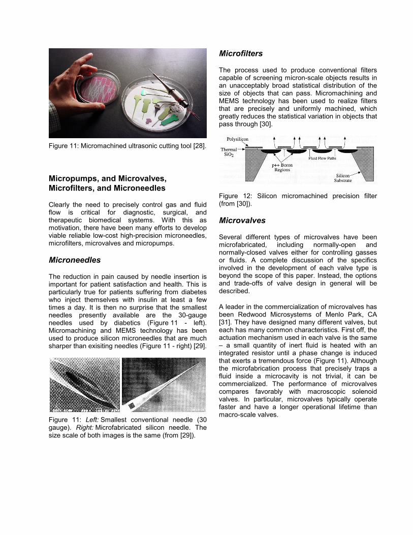
Figure 11: Micromachined ultrasonic cutting tool [28].
Micropumps, and Microvalves, Microfilters, and Microneedles
Clearly the need to precisely control gas and fluid flow is critical for diagnostic, surgical, and therapeutic biomedical systems. With this as motivation, there have been many efforts to develop viable reliable low-cost high-precision microneedles, microfilters, microvalves and micropumps.
Microneedles
The reduction in pain caused by needle insertion is important for patient satisfaction and health. This is particularly true for patients suffering from diabetes who inject themselves with insulin at least a few times a day. It is then no surprise that the smallest needles presently available are the 30-gauge needles used by diabetics (Figure 11 - left). Micromachining and MEMS technology has been used to produce silicon microneedles that are much sharper than exisiting needles (Figure 11 - right) [29].
Figure 11: Left: Smallest conventional needle (30 gauge). Right: Microfabricated silicon needle. The size scale of both images is the same (from [29]).
Microfilters
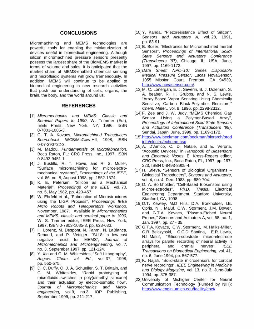
The process used to produce conventional filters capable of screening micron-scale objects results in an unacceptably broad statistical distribution of the size of objects that can pass. Micromachining and MEMS technology has been used to realize filters that are precisely and uniformly machined, which greatly reduces the statistical variation in objects that pass through [30].
Figure 12: Silicon micromachined precision filter (from [30]).
Microvalves
Several different types of microvalves have been microfabricated, including normally-open and normally-closed valves either for controlling gasses or fluids. A complete discussion of the specifics involved in the development of each valve type is beyond the scope of this paper. Instead, the options and trade-offs of valve design in general will be described.
A leader in the commercialization of microvalves has been Redwood Microsystems of Menlo Park, CA [31]. They have designed many different valves, but each has many common characteristics. First off, the actuation mechanism used in each valve is the same – a small quantity of inert fluid is heated with an integrated resistor until a phase change is induced that exerts a tremendous force (Figure 11). Although the microfabrication process that precisely traps a fluid inside a microcavity is not trivial, it can be commercialized. The performance of microvalves compares favorably with macroscopic solenoid valves. In particular, microvalves typically operate faster and have a longer operational lifetime than macro-scale valves.

Figure 11: Microvalves designed by Redwood Microsystems, Inc [31].
The TiNi corporation has also commercialized a micromachined pressure sensor driven by shape-memory alloys. HP and NovaSensor have designed, fabricated, and tested microvalves driven by the linear thermal expansion of solid materials. Despite the good performance, the HP valves have not yet been commercialized due to business reasons and the NovaSensor valves are in the final phase of development.
The performance of microvalves compares favorably with macroscopic solenoid valves. In particular, microvalves typically operate faster and have a longer operational lifetime. However, since microvalves are typically driven by thermal actuators their power consumption is still relatively high (0.1-2.0 W). Care must be taken to prevent the valve temperature to exceed that tolerated by the fluid or gas media being controlled.
Micropumps
Several methods of microactuation have been used to drive micropumps: electrostatic forces, magnetic forces, and piezoelectric. One example is a miniaturized gear pump that consists of LIGA microgears that are magnetically actuated It has been commercialized by MEMStek Products, LLC, of Vancouver, Washington [32]. Another example is an electrostatically driven micropump produced by bonding multiple bulk micromachined silicon wafers together. The bonding process creates a pumping cavity with a deformable membrane and two one-way check valves.
The electrodes are fabricated inside a second isolated cavity formed above the deformable pumping membrane so that they are sealed away from the conductive solutions being pumped (Figure 12). Although the micropump works well, high voltages (>100 V) are required for significant pumping to occur [33].
Figure 12: Electrostatic micropump with two one-way check valves (from [33]).
When designing micropumps for biomedical applications, attention must be paid to the media being pumped. Some fluids, such as insulin, cannot tolerate aggressive pumping mechanisms without degrading.
BIOMEDICAL MICROSYSTEMS
The ability to miniaturize entire biomedical systems, such as DNA analysis, chemical analysis, drug development, and neural prosthetics, has the potential to reduce the cost of health-care management. For example, reducing the cost and complexity of performing DNA screening and chemical analysis to the point that tests can be performed rapidly on the desktop, would reduce the infrastructure required for the test without compromising capability. This would enable remote or small-scale clinics to offer fast high-quality tests.
Microfluidic Systems
Chemical, pharmaceutical, and genetic analysis systems require the precise handling of fluids (i.e., sampling, mixing, heating, cooling, reacting, and separating). Conventional fluidic analyses are typically performed with relatively macroscopic fluidic systems (>25 µL). Miniaturization and integration of fluidic systems offers the following advantages: (1) smaller typical operating fluid volume, (2) precise

control of sample volumes, (3) ability to perform massively parallel tests, (4) take advantage of the effect of scaling on fluidic, electrical, and thermal behavior, (5) possible reduction in system size, and (6) possible reduction in system cost. One important caveat with miniaturizing fluidic analysis systems is the fact that reducing the sample size requires a corresponding increase in sensor sensitivity. In addition, micro-scale fluid flow is almost completely laminar (i.e., there is very little turbulence and thus mixing can be problematic).
Micro Total Analysis Systems (µTAS)
The ability to electrically control fluid flow in micromachined channels (i.e., pumping and valving) without any moving parts has enabled the realization of complex micro total analysis systems [34]. With multiple independently controlled flow channels, complex sample preparation, mixing, and testing procedures can be established. The electrically controlled pumping and valving mechanism is either electroosmotic flow or electrophoretic flow [2]. Liquid chromatography (i.e., a method of separating liquids based on their different mobility in a long flow channel) can be used to perform a precise chemical analysis in microfabricated flow channels. Sensors integrated at the end of the flow channel will reveal a time-domain spectrum of the fluid composition. Micromachined electrophoretic devices have been used to separate ions and DNA molecules from 70 to 1000 bases in under 2 minutes – much faster than conventional capillary electrophoresis systems [35]. The detection of each ion or molecule species can be accomplished with electrochemical measure-ments, fluorescence, or optical absorption.
Microsystems for Genetic Analysis
The analysis of genetic material typically calls for first the amplification of the DNA sample and then its detection. The amplification of a DNA sample can be accomplished by polymerase chain reaction (PCR). The PCR process begins by heating the DNA sample above the temperature at which the two strands separate or “melt” (~90 to 95ºC). If the DNA polymerase enzyme and the building blocks of DNA (i.e., nucleotide triphosphates) are present during cooling, the DNA polymerase will then reconstruct each double helix resulting in a doubling of the number of DNA stands. A major advantage of miniaturizing PCR systems is the fact that the much lower thermal mass of the reaction chamber allows for more rapid heating and cooling and thus a much faster process overall. Furthermore, it is even possible to integrate heaters and temperature
sensors into the same chip to allow for improved temperature control.
Figure Micromachined PCR chamber (from [36]).
Gene Chips
Separation by electrophoresis can be used to detect the size of a DNA molecule, but another method is needed to determine its precise code. One method exploits the highly selective hybridization process that allows DNA fragments to bind only with their complimentary sequence. In order to test for many specific sets of DNA sequences (i.e., for genetic screening), a large number of unique oligonucleotide probes need to be constructed and compared to the amplified DNA. One novel method of constructing oligonucleotide probes employs the same lithographic techniques used to construct MEMS. Specifically, a substrate is coated with a compound that is protected by a photochemically cleavable or photolabile protecting group (e.g., nitroveratryloxy-carbonyl).
When this film is exposed to a pattern of light, the illuminated regions will become unprotected and can be conditioned to receive a specific nucleotide / photolabile protecting group pair. By continuing the processes with a new mask pattern each time, very large arrays of unique combinations of nucleotide can be rapidly formed. The process is repeated until the desired oligonucleotides are constructed. After tagging the sample DNA with a fluorescent probe, it is then distributed over the array of oligonucleotide probes. Subsequent optical inspection of the distribution of fluorescence clearly indicates which oligonucleotides in the array match with a section of the sample DNA. Miniaturization of this detection system enabled massively parallel screening (i.e., 40,000 different compounds can be tested on a single 1 cm chip with 50 µm oligonucleotide probe areas. Affymetrix, Inc, has commercialized a DNA detection scheme based on this technology [37].
CONCLUSIONS
Micromachining and MEMS technologies are powerful tools for enabling the miniaturization of devices useful in biomedical engineering. Although silicon micromachined pressure sensors presently possess the largest share of the BioMEMS market in terms of volume and sales, it is anticipated that the market share of MEMS-enabled chemical sensing and microfluidic systems will grow tremendously. In addition, MEMS will continue to be applied to biomedical engineering in new research activities that push our understanding of cells, organs, the brain, the body, and the world around us.
REFERENCES
[1] Micromechanics and MEMS: Classic and Seminal Papers to 1990, W. Trimmer (Ed.), IEEE Press, New York, NY, 1996, ISBN 0-7803-1085-3.
[2] G. T. A. Kovacs, Micromachined Transducers Sourcebook. WCB/McGaw-Hill, 1998, ISBN 0-07-290722-3.
[3] M. Madou, Fundamentals of Microfabrication. Boca Raton, FL: CRC Press, Inc., 1997, ISBN 0-8493-9451-1.
[4] J. Bustillo, R. T. Howe, and R. S. Muller, “Surface micromachining for microelectro-mechanical systems”, Proceedings of the IEEE, vol. 86, no. 8, August 1998, pp. 1552-1574.
[5] K. E. Petersen, “Silicon as a Mechanical Material”, Proceedings of the IEEE, vol. 70, no. 5, May 1982, pp. 420-457.
[6] W. Ehrfeld et al., “Fabrication of Microstructures using the LIGA Process”, Proceedings IEEE Micro Robots and Teleoperators Workshop, November, 1987. Available in Micromechanics and MEMS: classic and seminal paper to 1990, W. S. Timmer editor, IEEE Press, New York, 1997, ISBN 0-7803-1085-3, pp. 623-633.
[7] H. Lorenz, M. Despont, N. Fahrnl, N. LaBianca, Renaud, and P. Vettiger, “SU-8: a low-cost negative resist for MEMS”, Journal of Micromechanics and Microengineering, vol. 7, no. 3, September 1997, pp. 121-124.
[8] Y. Xia and G. M. Whitesides, “Soft Lithography”, Angew. Chem. Int. Ed., vol. 37, 1998, pp. 550-575.
[9] D. C. Duffy, O. J. A. Schueller, S. T. Brittain, and G. M. Whitesides, “Rapid prototyping of microfluidic switches in poly(dimethyl siloxane) and their actuation by electro-osmotic flow”, Journal of Micromechanics and Micro-engineering, vol.9, no.3, IOP Publishing, September 1999, pp. 211-217.
[10] Y. Kanda, “Piezoresistance Effect of Silicon”, Sensors and Actuators A, vol. 28, 1991, pp. 83-91.
[11] B. Boser, “Electronics for Micromachined Inertial Sensors”, Proceedings of International Solid-State Sensors and Actuators Conference (Transducers '97), Chicago, IL, USA, June, 1997, pp. 1169-1172.
[12] Data Sheet: NPC–107 Series Disposable Medical Pressure Sensor, Lucas NovaSensor, 1055 Mission Court, Fremont, CA 94539, http://www.novasensor.com/.
[13] M. C. Lonergan, E. J. Severin, B. J. Doleman, S. A. beaber, R. H. Grubbs, and N. S. Lewis, “Array-Based Vapor Sensring Using Chemically Sensitive, Carbon Black-Polymber Resistors,” Chem. Mater., vol. 8, 1996, pp. 2298-2312.
[14] F. Zee and J. W. Judy, “MEMS Chemical Gas Sensor Using a Polymer-Based Array”, Proceedings of International Solid-State Sensors and Actuators Conference (Transducers '99), Sendai, Japan, June, 1999, pp. 1169-1172.
[15] http://www.beckman.com/beckman/biorsrch/prodinfo/electro/echome.asp
[16] A. D’Amico, C. Di Natale, and E. Verona, “Acoustic Devices,” in Handbook of Biosensors and Electronic Noses, E. Kress-Rogers editor, CRC Press, Inc., Boca Raton, FL, 1997, pp. 197-223, ISBN 0-8493-8905-4.
[17] H. Stieve, “Sensors of Biological Organisms – Biological Transducers”, Sensors and Actuators, vol. 4, no. 4, Dec. 1983, pp. 689-704.
[18] D. A. Borkholder, “Cell-Based Biosensors using Microelectrodes”, Ph.D. Thesis, Electrical Engineering Department, Stanford University, Stanford, CA, 1998.
[19] D.T. Kewley, M.D Hills, D.A. Borkholder, I.E. Opris, N.I. Maluf, C.W. Storment, J.M. Bower, and G.T.A. Kovacs, "Plasma-Etched Neural Probes," Sensors and Actuators A, vol. 58, no. 1, Jan. 1997, pp. 27 - 35.
[20] G.T.A. Kovacs, C.W. Storment, M. Halks-Miller, C.R. Belczynski, C.C.D. Santina, E.R. Lewis, N.I. Maluf, “Silicon-substrate micro-electrode arrays for parallel recording of neural activity in peripheral and cranial nerves”, IEEE Transactions on Biomedical Engineering, vol. 41, no. 6, June 1994, pp. 567-577.
[21] K. Najafi, “Solid-state microsensors for cortical nerve recordings”, IEEE Engineering in Medicine and Biology Magazine, vol. 13, no. 3, June-July 1994, pp. 375-387.
[22] University of Michigan Center for Neural Communication Technology (Funded by NIH): http://www.engin.umich.edu/facility/cnct/

[23] Stanford University research on microprobes: http://transducers.stanford.edu/stl/Projects.html
[24] University of Utah, Bioengineering Department: http://www.bioen.utah.edu/faculty/RAN/
[25] J. W. Judy, R. S. Muller, and H. H. Zappe, "Magnetic microactuation of polysilicon flexure structures," IEEE Journal of Microelectromechanical Systems, vol. 4, no. 4, pp. 162-169, 1995.
[26] A. P. Lee, D. R. Ciarlo, P. A. Krulevitch, S. Lehew, J. Trevino, and M. A. Northrup, “A Practical Microgripper by Fine Alignment, Eutectic Bonding and SMA Actuation”, Proceedings of International Solid-State Sensors and Actuators Conference (Transducers '95), Stockholm, Sweden, June, 1995, pp. 368-371.
[27] U.S. Patent 5,629,577 – Piezoelectric microactuator useful in a force-balanced scalpel.
[28] A. Lal, “Silicon-based ultrasonic surgical actuators”, Proceedings of the 20th Annual International Conference of the IEEE Engineering in Medicine and Biology Society, vol. 20, Hong Kong, China, 29 Oct. 1998, pp. 2785-2790.
[29] N.H. Talbot and A.P. Pisano, “Polymolding: two wafer polysilicon micromolding of closed-flow passages for microneedles and microfluidic devices”, Solid-State Sensor and Actuator Workshop Technical Digest, Hilton Head Island, SC, USA, 8-11 June 1998, pp. 265-268.
[30] W.-H. Chu, R. Chin, T. Huen, and M. Ferrari, “Silicon membrane nanofilters from sacrificial oxide removal”, Journal of Microelectro-mechanical Systems, vol. 8, no. 1, IEEE, March 1999, pp. 34-42.
[31] http://www.redwoodmicro.com/ [32] http://www.mems.com/ [33] R. Zengerle, J. Ulrich, S. Kluge M. Richter, A.
Richter, “A bidirectional silicon micropump”, Sensors and Actuators A (Physical), vol. A50, no. 1-2, Aug. 1995, pp. 81-86.
[34] N. Chiem, C. Colyer, and D.J. Harrison, “Microfluidic systems for clinical diagnostics”, International Conference on Solid-State Sensors and Actuators Digest of Technical Papers (Transducers '97), Chicago, IL, USA, 16-19 June 1997, pp. 183-186.
[35] A. T. Woolley and R. A. Mathies, “Ultra-High Speed DNA Fragment Separations Using Microfabricated Capillary Array Electrophoresis Chips", Proceedings of the National Academy of Science, vol. 91, Nov. 1994, pp. 11348-11352.
[36] M.A. Northrup, M.T. Ching, R.M. White, and R.T. Lawton, “DNA Amplification with a Microfabricated Reaction Chamber”, International Conference on Solid-State Sensors
and Actuators (Transducers 93), Yokohama, Japan, June 7-10, 1993, pp. 924-926.
[37] http://www.affymetrix.com/