Embed Size (px)
Citation preview
Biochemical sensing at the surface of graphene field-effect transistors
Wangyang Fu, Lin Jiang, Erik P. van Geest, Lia M. C. Lima, and Grégory F. Schneider*
Leiden University, Faculty of Science, Leiden Institute of Chemistry, Einsteinweg 55, 2333CC Leiden, 5
The Netherlands
* to whom correspondence should be addressed: [email protected]
Abstract. 10
Recent research trends now offer new opportunities for developing the next generations of label-free
biochemical sensors using graphene and other two-dimensional materials. While the physics of graphene
transistors operated in electrolyte is well grounded, important chemical challenges still remain to be addressed,
namely the impact of the chemical functionalizations of graphene on the key electrical parameters and the
sensing performances. In fact, graphene – at least ideal graphene – is highly chemically inert. The 15
functionalizations and chemical alterations of the graphene surface – both covalently and non-covalently – are
crucial steps that define the sensitivity of graphene. The presence, reactivity, adsorption of gas and ions, proteins,
DNA, cells and tissues on graphene have been successfully monitored with graphene. This review aims to unify
most of the work done so far on biochemical sensing at the surface of a (chemically functionalized) graphene
field-effect transistor and the challenges that lie ahead. We are convinced that graphene biochemical sensors 20
hold great promises to meet the ever-increasing demand for sensitivity, especially looking at the recent
progresses suggesting that the obstacle of Debye screening can be overcome.
2
Author description.
Dr. Wangyang Fu received his doctoral degree in physics from the Institute of Physics, Chinese Academy of
Sciences in 2009. Currently, Dr. Fu is a postdoctoral researcher in the group of Dr. Schneider at Leiden
University and recipient of a Veni grant (NWO) and an APM grant (SNF) for young researchers. Prior to
joining the Leiden group in 2015, he was a postdoctoral researcher at University of Basel with Prof. Christian 5
Schönenberger and at the Jülich Research Center with Prof. Andreas Offenhäusser (Humboldt, AvH). His
research interests focus on graphene nanoelectronics for biochemical sensing.
Lin Jiang is a PhD student in the group of Dr. Schneider at Leiden University. She received her MSc degree in
chemistry from Shanghai University, China. Her current research interests focus on graphene defects generation 10
for chemical (electrochemical) biosensing applications.
Dr. Grégory F. Schneider received his PhD in chemistry from the University of Strasbourg in 2005. Grégory is
currently principal investigator and tenure track assistant professor of chemistry at the Leiden Institute of
Chemistry. He received in 2014 an ERC starting grant and a Vidi grant from NWO to carry chemical and 15
biological research with graphene. Prior to joining the Leiden faculty in 2013, he was a postdoctoral researcher
3
at Harvard University with Prof. George Whitesides and at TU Delft with Prof. Cees Dekker. His research
interests include nanotechnology, bionanotechnology, surface and interfacial chemistry, physical and organic
chemistry, materials science, biophysical chemistry, nanofluidics, and self-assembly.
5
4
Table of contents.
This review aims to unify most of the work done so far on biochemical sensing at the surface of a (chemically
functionalized) graphene field-effect transistor and the challenges that lie ahead, including the recent progresses 5
in meeting the ever increasing demand for sensitivity by overcoming the obstacle of Debye screening.
1. Introduction: challenges and opportunities
2. Physics of graphene field-effect transistors (GFETs): the basics for sensing
2.1. Back-gated GFETs
2.2. Liquid-gated GFETs: operation and sensing principle 10
2.3. Sensing with graphene of high carrier mobility
2.4. Electrical noise performance of graphene materials
2.5. Debye screening
3. Meeting the challenges in chemical functionalizations of graphene for biochemical sensing
3.1. Covalent functionalizations 15
3.2. Non-covalent functionalizations
3.3. Graphene lipid superstructures: towards graphene bioelectronics
4. Current trends & efforts in biochemical sensing at the surface of GFETs
4.1. GFET gas and ion sensors
4.2. GFET glucose, DNA, and protein bioensors 20
4.3. GFET biological cellular sensors
4.4. Graphene-based electrochemical (GEC) biosensors
5. Perspectives and conclusions
---
Vref
Vsd
reference electrode
target biomolecule
+
graphene
receptor
movable ions

5
5.1. Graphene as a chemically inert surface: towards an ultimate biosensor
5.2. Overcoming the Debye length limitations with radio-frequency (RF)-operated GFETs
6
1. Introduction: challenges and opportunities
Ultrasensitive biosensors are opening up new opportunities for ‘personalized medicine’ tailored to the specific
biochemistry and diagnostic of individual patients.[1, 2] While versatile detection strategies exist, the main
requirements for a biosensor is that the detection is sensitive (identification of clinically relevant concentrations of
biomarkers in biological samples) and selective (availability of a suitable biological recognition element).[3] Since
the experimental preparation and observation of the electric field effect in graphene by the Manchester group in
2004,[4] biochemical sensing using graphene electronic devices has been actively pursued.[5-12] The sensing
principle roots on a change of the electrical conductance of the graphene channel upon adsorption of a molecule on
the sensor surface.[5] The uniqueness of graphene among other solid-state materials is that all carbon atoms are
located on the surface, making the graphene surface potentially highly sensitive to any changes of its surrounding
environment. Along with the excellent electrical properties of graphene,[13, 14] i.e., extraordinary high mobility[15, 16,
17] and low intrinsic electrical noise,[18-21] graphene-based electronic biosensors demonstrated greater sensitivity
than traditional bioassays.[22] Additionally, graphene (at least ideal graphene) has a crystal lattice free of dangling
bonds and is therefore intrinsically chemically inert. This inertness has been a driving force for the first attempts
aiming at biointerfacing graphene with specific recognition moieties, via both covalent[23-27, 28] and non-covalent[29-
32] approaches, using different biochemical molecules and chemical treatments.
This article aims to provide a comprehensive overview and critical insights on biosensors using the surface of
graphene as the sensing element. We evaluate the electronic and the chemical advantages of graphene, i.e., the
high carrier mobility, low intrinsic electrical noise and the inert chemical properties, which are at the core of the
sensing mechanisms but also crucial in applications where graphene must be interfaced with biological systems.
Particularly, we highlight the importance of the chemistry of the graphene basal plane for sensing within the
Debye screening length and shed light on the possibilities of sensing beyond the Debye screening.
2. Physics of graphene field-effect transistors (GFETs): the basics for sensing
Graphene nanoelectronics provide a versatile platform for a wide spectrum of biochemical sensing applications.[33]
Detection can be realized through various mechanisms, including charge transfer,[34] charge scattering,[35]
7
capacitive effect,[36] and field effects.[6, 7, 37] The field effect (i.e., the modulation of the electrical conductivity of a
material upon the application of an external electric field, for example, induced by a charged biomolecule) has
been widely regarded as the most reliable sensing mechanism. This effect has been harvested to design the first
graphene field-effect transistor (GFET),[4] which has inspired considerable experimental and theoretical work
relating to the application of GFETs for high performance label-free chemical and biological sensors.[5-12, 37]
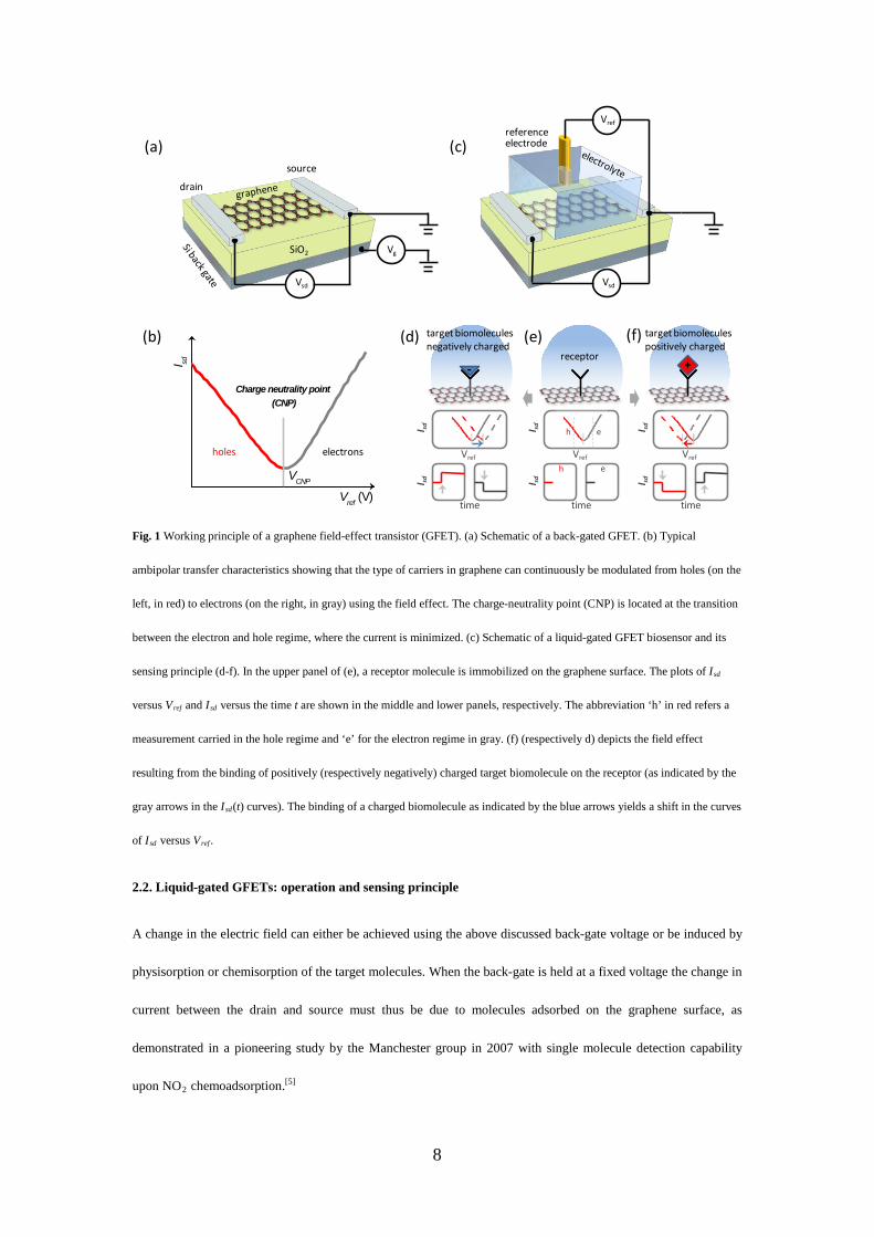
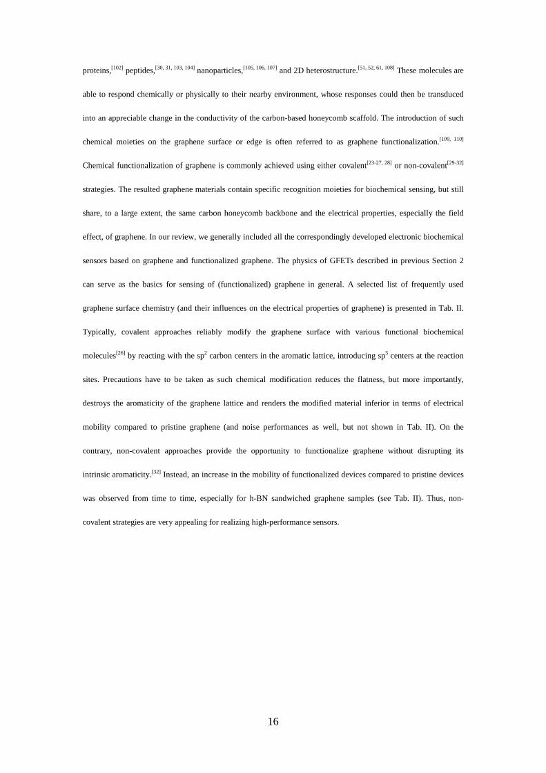
2.1. Back-gated GFETs.
The word transistor is a combination of two words: transfer and resistor. Usually a transistor is used to switch or
amplify an electronic signal, comparable to a tap-valve that controls the supply and flow of water. Fig. 1a depicts a
back-gated GFET composed of a source/drain metallic electrode bridged together with a graphene channel. The
carrier density, and thus the conductivity of the channel is typically modulated by the electric field by gating a
highly conductive silicon substrate located underneath an insulating SiO2 dielectric layer to a range of voltages. As
shown in Fig. 1b, a typical measurement consists in applying a constant bias voltage, Vsd, between the source and
the drain of the graphene channel, and monitor the resulting source-drain current Isd. A direct consequence of the
electronic band structure of graphene[4, 14] is that graphene-based FET devices are of metallic nature and cannot be
switched off at room temperature. Besides chemical modification, graphene nanoribbon, graphene nanomesh, and
graphene nanoring,[38] have also been proved as rational designs of the graphene to open a bandgap, yielding an
improved transistor Ion/Ioff ratio. Nevertheless, the transistor Ion/Ioff ratio has no direct relation to the performances
of a sensor device, although it is related to graphene digital applications requiring high on state current (Ion) and
ultra-low power consumption at the off state (Ioff) of the transistors. By changing the back gate voltage Vg, the
electrochemical potential of the charge carriers (i.e., the Fermi energy) can be modulated. As a consequence, the
type of charge carriers (which flow in the graphene channel and give the current Isd) can continuously be tuned
from holes (red curve in the left of Fig. 1b) to electrons (gray curve in the right of Fig. 1b), yielding a so-called
'ambipolar behavior'. At the transition between the electron and hole regime, the current is minimized and this
point is also known as the charge neutrality point (CNP).
8
Fig. 1 Working principle of a graphene field-effect transistor (GFET). (a) Schematic of a back-gated GFET. (b) Typical
ambipolar transfer characteristics showing that the type of carriers in graphene can continuously be modulated from holes (on the
left, in red) to electrons (on the right, in gray) using the field effect. The charge-neutrality point (CNP) is located at the transition
between the electron and hole regime, where the current is minimized. (c) Schematic of a liquid-gated GFET biosensor and its
sensing principle (d-f). In the upper panel of (e), a receptor molecule is immobilized on the graphene surface. The plots of Isd
versus Vref and Isd versus the time t are shown in the middle and lower panels, respectively. The abbreviation ‘h’ in red refers a
measurement carried in the hole regime and ‘e’ for the electron regime in gray. (f) (respectively d) depicts the field effect
resulting from the binding of positively (respectively negatively) charged target biomolecule on the receptor (as indicated by the
gray arrows in the Isd(t) curves). The binding of a charged biomolecule as indicated by the blue arrows yields a shift in the curves
of Isd versus Vref .
2.2. Liquid-gated GFETs: operation and sensing principle
A change in the electric field can either be achieved using the above discussed back-gate voltage or be induced by
physisorption or chemisorption of the target molecules. When the back-gate is held at a fixed voltage the change in
current between the drain and source must thus be due to molecules adsorbed on the graphene surface, as
demonstrated in a pioneering study by the Manchester group in 2007 with single molecule detection capability
upon NO2 chemoadsorption.[5]
Vref
Vsd
drain
source
SiO2
reference electrode
Vsd
Vg
VCNP
Charge neutrality point (CNP)
I sd
Vref (V)
holes electrons
target biomoleculespositively charged
receptor
target biomoleculesnegatively charged
time time time
Vref Vref Vref
I sd
h e
I sd
I sdI sd
I sdI sd
h e
- +
(a)
(b)
(c)
(d) (e) (f)
9
In contrast to the back-gate geometry, in a liquid-gated configuration the gate voltage is applied to the
electrolyte via a reference electrode (Fig. 1c). The reference electrode is coupled to the graphene channel through
an interfacial capacitance C, consisting of a series of two capacitances,[37] namely the quantum capacitance of
graphene (CQ),[39] and the double layer capacitance of the electrolyte (CDL).[40] The double layer capacitor is a
virtual capacitor formed by the separated charges located at the solid side and the solution side of the interface as
described by the Poisson-Boltzmann equation.[41] Liquid-gated GFET biosensors belong to the large family of ion-
sensitive FETs, the first new concept of which was investigated by Bergveld with Si devices.[42, 43] Although the
choice of the channel materials, the reference electrode, the operational mode, and the final encapsulation for
liquid handling, vary from case to case, the heart of any ion-sensitive FETs lies on the interface between
electrolyte and the solid FET material. In general, GFETs are operated at low electrolyte gate voltage such that any
electrochemical processes and exchange ionic currents are negligible, i.e., the interface is considered to be inert
and purely capacitive, although this assumption is not always explicitly stated in most of the literature.
Experimental artifacts at moderate or relatively high electrolyte gate voltages resulting from such simple
assumption are considered mainly of electrochemical nature that will be separately discussed in Section 4.4:
Graphene-based electrochemical (GEC) biosensors.
The working principle of a liquid-gated GFET biosensor is illustrated in Fig. 1d-f. In practice, liquid-gated
GFETs can be integrated into microfluidic systems:[22] the confinement into the fluidic channel helps in bringing
the analyte to the sensor surface.[44] In a typical measurement, receptor molecules are immobilized on the surface
for selective recognition of target biomolecules (Fig. 1e, upper panel). The corresponding Isd versus Vref curve of
such a liquid-gated GFET is shown in the middle panel (Fig. 1e) with similar characteristics as the one observed
for a back-gated GFET (Fig. 1b). The lower panel of Fig. 1e depicts the time dependent current Isd at a fixed
reference potential Vref (as indicated by the dashed gray lines). In either the hole regime (as indicated by ‘h’) or in
the electron regime (‘e’), when a positively charged target binds (Fig. 1f, upper panel), a depletion of hole carriers
(respectively an accumulation of electron carriers) in the graphene occurs due to the field effect. Such doping
effect causes a negative shift of the Isd(Vref) curve as indicated by the blue arrow in Fig. 1f (middle panel).
In the time-dependent measurement (i.e., the lower panel of Fig. 1f), the binding of a positively charged
molecule causes a decrease of the current Isd in the hole regime, and an increase of the current in the electron
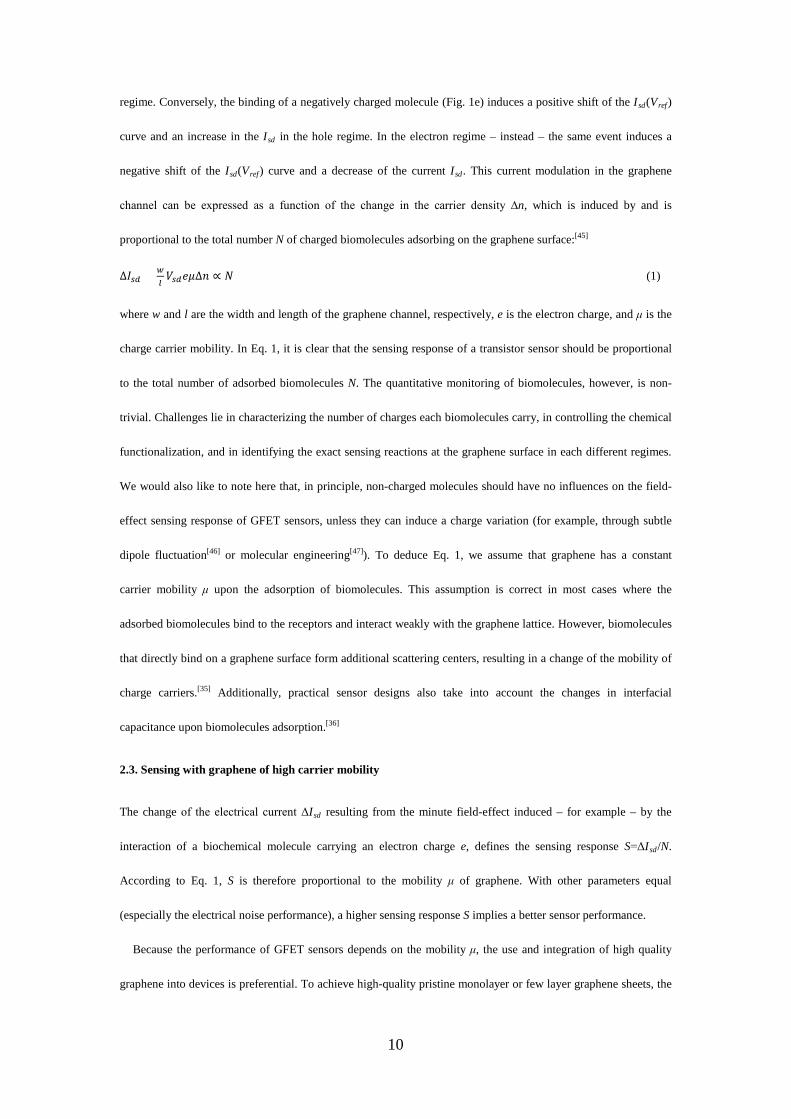
10
regime. Conversely, the binding of a negatively charged molecule (Fig. 1e) induces a positive shift of the Isd(Vref)
curve and an increase in the Isd in the hole regime. In the electron regime – instead – the same event induces a
negative shift of the Isd(Vref) curve and a decrease of the current Isd. This current modulation in the graphene
channel can be expressed as a function of the change in the carrier density ∆n, which is induced by and is
proportional to the total number N of charged biomolecules adsorbing on the graphene surface:[45]
∆𝐼𝑠𝑠 = 𝑤𝑙𝑉𝑠𝑠𝑒𝑒∆𝑛 ∝ 𝑁 (1)
where w and l are the width and length of the graphene channel, respectively, e is the electron charge, and μ is the
charge carrier mobility. In Eq. 1, it is clear that the sensing response of a transistor sensor should be proportional
to the total number of adsorbed biomolecules N. The quantitative monitoring of biomolecules, however, is non-
trivial. Challenges lie in characterizing the number of charges each biomolecules carry, in controlling the chemical
functionalization, and in identifying the exact sensing reactions at the graphene surface in each different regimes.
We would also like to note here that, in principle, non-charged molecules should have no influences on the field-
effect sensing response of GFET sensors, unless they can induce a charge variation (for example, through subtle
dipole fluctuation[46] or molecular engineering[47]). To deduce Eq. 1, we assume that graphene has a constant
carrier mobility μ upon the adsorption of biomolecules. This assumption is correct in most cases where the
adsorbed biomolecules bind to the receptors and interact weakly with the graphene lattice. However, biomolecules
that directly bind on a graphene surface form additional scattering centers, resulting in a change of the mobility of
charge carriers.[35] Additionally, practical sensor designs also take into account the changes in interfacial
capacitance upon biomolecules adsorption.[36]
2.3. Sensing with graphene of high carrier mobility
The change of the electrical current ΔIsd resulting from the minute field-effect induced – for example – by the
interaction of a biochemical molecule carrying an electron charge e, defines the sensing response S=ΔIsd/N.
According to Eq. 1, S is therefore proportional to the mobility μ of graphene. With other parameters equal
(especially the electrical noise performance), a higher sensing response S implies a better sensor performance.
Because the performance of GFET sensors depends on the mobility μ, the use and integration of high quality
graphene into devices is preferential. To achieve high-quality pristine monolayer or few layer graphene sheets, the
11
most commonly used method is the micromechanical cleavage of graphite with adhesive tape.[4] This so-called
‘scotch tape’ technique involves splitting few layers of graphene from multi-layered graphite, after which the
flakes are pressed and ‘dry-deposited’ onto a silicon wafer. Compared to graphene synthesized using other
methods, micromechanical cleavage yields graphene with higher mobility and lower intrinsic electrical noise,
primarily because fewer structural defects are introduced upon preparation.[48] Generally, for exfoliated graphene
on SiO2/Si wafers, mobilities on the order of ~3,000-15,000 cm2/Vs are reported,[49] which is more than one order
of magnitude higher than those of silicon materials (~100-1,500 cm2/Vs).[1, 50] The mobilities of the first graphene-
based gas sensor devices were ~5,000 cm2/Vs.[5] Nowadays, at room temperature, carrier mobility up to 100,000-
197,600 cm2/Vs, can be achieved by encapsulating graphene in boron nitride (BN),[17, 51, 52] providing
unprecedented possibilities for sensing applications. The fact that this idea has only been realized very recently
(with h-BN capped MoS2[53]) is not a surprise: groups that work on high quality BN coated graphene samples, very
often focus on cryogenic measurements of the physics of the 2D electron gases in graphene rather than its
biological sensing applications; moreover, the fabrication methods are very delicate (it is not yet trivial to achieve
an ideal interface) and the lack of scalability is still an important drawback.[17]
Despite all the impressive achievements in the electrical performances of graphene devices, the reproducibility
and homogeneity of sample preparation and the relatively small size (on micrometer scale) represent the
bottleneck for using exfoliated graphene for practical applications. Larger sheets of few-layer or monolayer
graphene can now be directly synthesized via chemical vapor deposition (CVD) on nickel or copper substrates[54,
55] with mobilities rivalling the ones of exfoliated samples.[56] For samples placed on SiO2/Si wafers, mobilities on
the order of ~1,000-10,000 cm2/Vs are now routinely observed and regarded as the standard for graphene transistor
products for biochemical sensing applications.[57] The electronic performances of CVD graphene[58] can be
significantly enhanced by growing single-crystal graphene free of grain boundaries[59] and by using a BN substrate
similarly to exfoliated graphene, with which mobility up to ~50,000-350,000 cm2/Vs can be achieved.[60, 61] These
mobility numbers are rivaling those of exfoliated samples, making the CVD process ideal for large-area synthesis
of high-quality and uniform graphene for sensing applications.
2.4. Electrical noise performances of graphene materials
At low frequencies (≲100 Hz), the ubiquitous 1/f noise, whose power spectral density (PSD) spectrum inversely
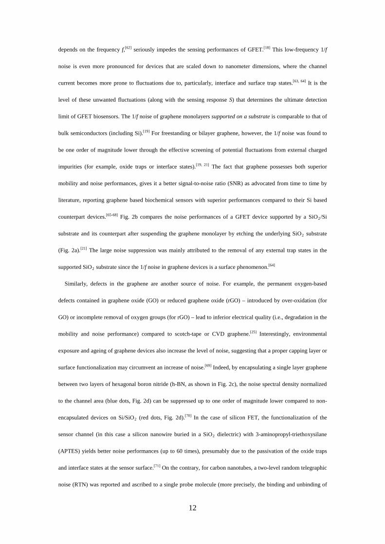
12
depends on the frequency f,[62] seriously impedes the sensing performances of GFET.[18] This low-frequency 1/f
noise is even more pronounced for devices that are scaled down to nanometer dimensions, where the channel
current becomes more prone to fluctuations due to, particularly, interface and surface trap states.[63, 64] It is the
level of these unwanted fluctuations (along with the sensing response S) that determines the ultimate detection
limit of GFET biosensors. The 1/f noise of graphene monolayers supported on a substrate is comparable to that of
bulk semiconductors (including Si).[19] For freestanding or bilayer graphene, however, the 1/f noise was found to
be one order of magnitude lower through the effective screening of potential fluctuations from external charged
impurities (for example, oxide traps or interface states).[19, 21] The fact that graphene possesses both superior
mobility and noise performances, gives it a better signal-to-noise ratio (SNR) as advocated from time to time by
literature, reporting graphene based biochemical sensors with superior performances compared to their Si based
counterpart devices.[65-68] Fig. 2b compares the noise performances of a GFET device supported by a SiO2/Si
substrate and its counterpart after suspending the graphene monolayer by etching the underlying SiO2 substrate
(Fig. 2a).[21] The large noise suppression was mainly attributed to the removal of any external trap states in the
supported SiO2 substrate since the 1/f noise in graphene devices is a surface phenomenon.[64]
Similarly, defects in the graphene are another source of noise. For example, the permanent oxygen-based
defects contained in graphene oxide (GO) or reduced graphene oxide (rGO) – introduced by over-oxidation (for
GO) or incomplete removal of oxygen groups (for rGO) – lead to inferior electrical quality (i.e., degradation in the
mobility and noise performance) compared to scotch-tape or CVD graphene.[25] Interestingly, environmental
exposure and ageing of graphene devices also increase the level of noise, suggesting that a proper capping layer or
surface functionalization may circumvent an increase of noise.[69] Indeed, by encapsulating a single layer graphene
between two layers of hexagonal boron nitride (h-BN, as shown in Fig. 2c), the noise spectral density normalized
to the channel area (blue dots, Fig. 2d) can be suppressed up to one order of magnitude lower compared to non-
encapsulated devices on Si/SiO2 (red dots, Fig. 2d).[70] In the case of silicon FET, the functionalization of the
sensor channel (in this case a silicon nanowire buried in a SiO2 dielectric) with 3-aminopropyl-triethoxysilane
(APTES) yields better noise performances (up to 60 times), presumably due to the passivation of the oxide traps
and interface states at the sensor surface.[71] On the contrary, for carbon nanotubes, a two-level random telegraphic
noise (RTN) was reported and ascribed to a single probe molecule (more precisely, the binding and unbinding of
13
charged target biomolecules at its active sites), which was covalently bound to a defect in the carbon nanotube
sidewall.[72] A suppression of the RTN was observed in high ionic strength buffer solutions (ionic screening) and
for high gate potentials (when the target biomolecules are repelled from the nanotube). The influence of surface
functionalization on the noise performances of liquid-gated GFETs has not yet been systematically studied. As we
described in the previous Section 2.3, with other parameters equal (especially the electrical noise performance), a
higher mobility implies a better sensor performance when considering the adsorption of charged biomolecules. We
would like to note here that a higher mobility also complies with graphene bearing less defects and impurities,
which is in favor of an improved noise performance (although there is still not enough experimental evidences or
theories that could directly and unambiguously link the high mobility of GFETs to their noise performances).
Fig. 2 (a) Schematic representation of the experimental setup where a single-layer graphene is supported in solution by Cr/Au
contacts to bridge a trench in the oxide. The inset shows an SEM image of a suspended graphene device. Scale bar is 0.5 μm. (b)
Comparison of graphene’s noise power spectra in the linear operating modes with holes as carriers before (black) and after
suspension of the graphene layer (red). The red/black spikes are due to 50 Hz noise coupled from the power lines. (c) Schematics
of BN-graphene-BN FET. (d) Noise amplitude as a function of the gate voltage for both BN-graphene-BN FET (in blue) and
conventional non-encapsulated GFET on Si/SiO2 wafer (in red). (e) The biomolecules carry zero net charge due to the Debye
screening effect of ions in electrolyte. (f) Relative changes in resistance (ΔR/R) of a carbon nanotube transistor versus buffer
concentration. Increasing the buffer concentration will reduce the Debye length (λD) so that most of the DNA’s negative charge
will be screened by counter ions in the electrolyte, resulting in a decreased sensing response (ΔR/R). Inset: schematic
representation of a DNA molecule binds on the sidewall of a carbon nanotube. Reprinted with permission.
(a) (c)
(b) (d) (f)
channelsource drain
---
Debye screening
+--
- + ---+
--- +
--
- +
(e)
Debye length
14
2.5. Debye screening
The true potential of graphene sensors in physiological solutions (and electrical sensors in general) is still behind
expectations. This is because that GFETs are primarily sensitive to the charges carried by the biomolecules
adsorbed on graphene surface, which suffer from the ionic screening due to mobile ions present in the solution,
known as Debye screening effect.[73] In electrolytes, this screening effect is characterized by the Debye length,
which is the measure of how far a charge carrier's net electrostatic effect persists, outside of which charges are
effectively screened and only 36.8 % (1/e, e=2.72) of the charges can still be seen by the graphene sensing devices.
This screening layer (or diffuse layer) is composed of movable ions attracted to a charged surface via the Coulomb
force (Fig. 2e). The Debye screening effect is an intrinsic thermodynamic property of large systems of mobile
charges. In the following we will examine the Debye screening dilemma in details and look into recent progresses.
For aqueous solutions at room temperature, the Debye length (in unit of nanometer) is given by:[74]
λD=0.304/I1/2, where I is the ionic strength expressed in mol/L (M), and is typically ~0.7 nm in physiological
conditions. Given the typical several nanometer size of biomolecules, it is therefore likely only small – or even no
net electrostatic effect – can be recorded by the transistor (see Fig. 2e). In Tab. I, we have summarized the sensing
responses of several ion-sensitive FETs (including nanowire, nanotube and graphene ion-sensitive FETs) at
different salt concentrations and biomolecule-to-sensor distances. Indeed, under physiological conditions of
1×PBS (λD~0.7 nm) and near side distance of ~1 nm (for example for biotin receptors anchored on the transistor
surface), nanowire ion-sensitive FETs showed no response upon the binding of streptavidin from a 10 nM
solution.[74] Even at low salt concentrations, the sensing response upon hybridization of complementary DNA
molecules (i.e., the normalized resistance change) was found to decrease dramatically from 80 % to 12 % by
increasing the buffer concentration from 0.1×PBS to 1×PBS in a manner that follows the Debye length
considerations (as given by the black fitting line in Fig. 2f).[72] Increasing further the buffer concentration to
10×PBS resulted in a full screening of the biological binding signal even at a relatively high DNA concentration of
1 μM.
15
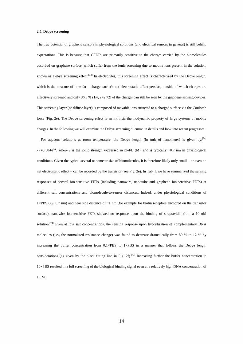
Tab. I. Selected summary of Debye screening length limitation
Surface modification + Target biomolecules
DistanceI Debye length λD (buffersII)
Concentration & relative sensitivity (ΔR/R)
Refs (comments)
Biotin + Streptavidin
~1 nm ~7 nm (0.01×PBS) 10 nM ~15 % [74] Nanowire
~0.7 nm (1×PBS) ~0 %
ssDNA + ssDNA (complementary)
At surface ~3 nm (0.05×PBS) 10 pM ~15-40 % [74] Nanowire ~1.4 nm ~2 nm (0.1×PBS) 1 μM ~80 % [72] Nanotube
~0.7 nm (1×PBS) ~12 % ~0.2 nm (10×PBS) ~0 %
ssPNA + ssDNA
2.6 nm (fully complementary)
~10 nm (0.01×SSC)
1 pM (1 nM)
~19 % (~51 %)
[75] Nanowire
7.7 nm (noncomplementary)
1 nM ~0 %
APTESIII + PSAIV
~0.8 nm ~7 nm (1 mM PB) 100 nM ~112 mV* [76] Nanowire
~2 nm (10 mM PB) ~8 mV* ~1 nm (50 mM PB) ~0
Bare graphene + BSAV (nonspecific)
At surface ~2 nm (10 mM PBS) 300 pM ~2 % [10] Graphene
20-mer DNA aptamer + ATPVI
<2.6 nm ~2-3 nm (5-10 mM PB)
10 pM ~1 % [77] Graphene
PSA monoclonal antibody + PSAIV
<15 nm ~70 nm (1 μM PBS) ~1 nM ~17 % [78] Graphene
~1 pM ~12 % ~1 fM ~2 %
I Near side distance of the target biomolecules from the device surface II Please refer to the according literature for the exact background ionic strength and pH value of the buffer solutions III Prostate specific antigen, prostate cancer biomarker IV (3-aminopropyl)-triethoxysilane V Bovine serum albumin
VI Adenosine triphosphate * Relative changes not given
N.B.: T = 293K unless stated otherwise. The Debye screening effect has put a fundamental limit to the possible applications of the graphene ion-
sensitive FETs (and ion-sensitive FETs in general) for biosensing applications, although ion-sensitive FETs can, in
principle, be sensitive to changes below one single charge.[5, 79] There are numerous evidences in the literature that
the sensing performances can be improved by circumventing the Debye screening effect, for example by designing
short antibodies, by performing ex situ measurement in low ionic strength buffers, and by incorporating porous
polymer layers permeable to biomolecules (Tab. I).[74-77, 80] At the end of this review, we will discuss in details that
recent progresses on operating GFETs at high frequencies suggested that Debye screening can be overcome:[46] 1.
without any special design or engineering of the receptor molecules and the sensor environments, and 2. in
physiological conditions to facilitate in-situ, real-time biosensing.
3. Meeting the challenges in chemical functionalization of graphene for biochemical
sensing
Due to its large aromatic sp2 carbon lattice, free of dangling bonds, graphene is intrinsically chemically inert.[12]
The broad sensing potential of graphene can only be unlocked by the introduction of sensitizer (bio)molecules and
structures, e.g. various inorganic groups,[23-25, 81-90] organic or organometallic molecules,[37, 91-93, 94-96] DNAs,[97-101]
16
proteins,[102] peptides,[30, 31, 103, 104] nanoparticles,[105, 106, 107] and 2D heterostructure.[51, 52, 61, 108] These molecules are
able to respond chemically or physically to their nearby environment, whose responses could then be transduced
into an appreciable change in the conductivity of the carbon-based honeycomb scaffold. The introduction of such
chemical moieties on the graphene surface or edge is often referred to as graphene functionalization.[109, 110]
Chemical functionalization of graphene is commonly achieved using either covalent[23-27, 28] or non-covalent[29-32]
strategies. The resulted graphene materials contain specific recognition moieties for biochemical sensing, but still
share, to a large extent, the same carbon honeycomb backbone and the electrical properties, especially the field
effect, of graphene. In our review, we generally included all the correspondingly developed electronic biochemical
sensors based on graphene and functionalized graphene. The physics of GFETs described in previous Section 2
can serve as the basics for sensing of (functionalized) graphene in general. A selected list of frequently used
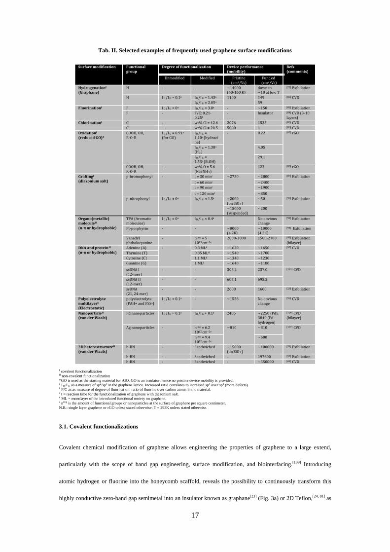
graphene surface chemistry (and their influences on the electrical properties of graphene) is presented in Tab. II.
Typically, covalent approaches reliably modify the graphene surface with various functional biochemical
molecules[26] by reacting with the sp2 carbon centers in the aromatic lattice, introducing sp3 centers at the reaction
sites. Precautions have to be taken as such chemical modification reduces the flatness, but more importantly,
destroys the aromaticity of the graphene lattice and renders the modified material inferior in terms of electrical
mobility compared to pristine graphene (and noise performances as well, but not shown in Tab. II). On the
contrary, non-covalent approaches provide the opportunity to functionalize graphene without disrupting its
intrinsic aromaticity.[32] Instead, an increase in the mobility of functionalized devices compared to pristine devices
was observed from time to time, especially for h-BN sandwiched graphene samples (see Tab. II). Thus, non-
covalent strategies are very appealing for realizing high-performance sensors.
17
Tab. II. Selected examples of frequently used graphene surface modifications
Surface modification Functional group
Degree of functionalization Device performance (mobility)
Refs (comments)
Unmodified Modified Pristine (cm2/Vs)
Func.ed (cm2/Vs)
HydrogenationI (Graphane)
H - - ~14000 (40-160 K)
down to ~10 at low T
[23] Exfoliation
H I D /I G = 0.1a I D /I G = 1.43a 1100
149 [82] CVD I D /I G = 2.05a 59
FluorinationI F I D /I G = 0a I D /I G = 3.8a - ~150 [83] Exfoliation F
- F/C: 0.21-0.25b
-
Insulator [84] CVD (3-10 layers)
ChlorinationI Cl - wt% Cl = 42.6 2076 1535 [85] CVD Cl - wt% Cl = 20.5 5000 1 [86] CVD
OxidationI (reduced GO)*
COOH, OH, R-O-R
I D /I G = 0.91a
(for GO)
I D /I G = 1.10a (hydrazine)
- 0.22 [87] rGO
I D /I G = 1.38a
(H 2 ) 4.05
I D /I G = 1.53a (EtOH)
29.1
COOH, OH, R-O-R
- wt% O = 5.6 (Na/NH 3 )
- 123 [88] rGO
GraftingI (diazonium salt)
p-bromophenyl - t = 30 minc ~2750 ~2800 [89] Exfoliation t = 60 minc ~2400 t = 90 minc ~1900 t = 120 minc ~850
p-nitrophenyl I D /I G ≈ 0a I D /I G ≈ 1.5a ~2000 (on SiO 2 )
~50
[90] Exfoliation
~15000 (suspended)
~200
Organo(metallic) moleculeII (π-π or hydrophobic)
TPA (Aromatic molecules)
I D /I G ≈ 0a I D /I G ≈ 0.4a - No obvious change
[91] Exfoliation
Pt-porphyrin - - ~8000 (4.2K)
~10000 (4.2K)
[94] Exfoliation
Vanadyl phthalocyanine
- nimp = 5 × 1013 cm−2e
2000-3000 1500-2300 [95] Exfoliation (bilayer)
DNA and protein II (π-π or hydrophobic)
Adenine (A) - 0.8 MLd ~1620 ~1650 [97] CVD Thymine (T) 0.85 MLd ~1540 ~1700 Cytosine (C) 1.1 MLd ~1340 ~1230 Guanine (G) 1 MLd ~1640 ~1180 ssDNA I (12-mer)
- - 305.2 237.0 [101] CVD
ssDNA II (12-mer)
- - 607.1 695.2
ssDNA (21, 24-mer)
- - 2600 1600 [29] Exfoliation
Polyelectrolyte multilayerII (Electrostatic)
polyelectrolyte (PAH+ and PSS-)
I D /I G ≈ 0.1a - ~1556
No obvious change
[96] CVD
NanoparticleII (van der Waals)
Pd nanoparticles I D /I G ≈ 0.1a I D /I G ≈ 0.1a 2405 ~2250 (Pd), 3840 (Pd-hydrogen)
[106] CVD (bilayer)
Ag nanoparticles -
nimp = 6.2 × 1012 cm−2e
~810 ~810 [107] CVD
nimp = 9.4 × 1012 cm−2e
~600
2D heterostructureII (van der Waals)
h-BN - Sandwiched ~15000 (on SiO 2 )
~100000 [51] Exfoliation
h-BN - Sandwiched - 197600 [52] Exfoliation h-BN - Sandwiched - ~350000 [61] CVD
I covalent functionalization II non-covalent functionalization *GO is used as the starting material for rGO. GO is an insulator; hence no pristine device mobility is provided. a I D /I G as a measure of sp2/sp3 in the graphene lattice. Increased ratio correlates to increased sp3 over sp2 (more defects). b F/C as as measure of degree of fluorination: ratio of fluorine over carbon atoms in the material. c t = reaction time for the functionalization of graphene with diazonium salt. d ML = monolayer of the introduced functional moiety on graphene. e nimp is the amount of functional groups or nanoparticles at the surface of graphene per square centimeter. N.B.: single layer graphene or rGO unless stated otherwise; T = 293K unless stated otherwise.
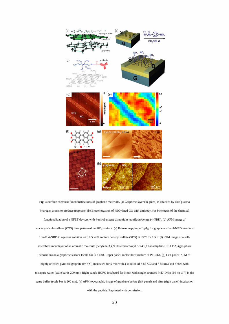
3.1. Covalent functionalizations
Covalent chemical modification of graphene allows engineering the properties of graphene to a large extend,
particularly with the scope of band gap engineering, surface modification, and biointerfacing.[109] Introducing
atomic hydrogen or fluorine into the honeycomb scaffold, reveals the possibility to continuously transform this
highly conductive zero-band gap semimetal into an insulator known as graphane[23] (Fig. 3a) or 2D Teflon,[24, 81] as
18
initially proposed by the Manchester group. Regarding sensing applications, calculations showed that (partially)
hydrogenated graphene has a high affinity for NO2;[111] while graphane doped with Li adatoms was predicted to be
sensitive to H2S and NH3.[112] Moreover, the reduced carrier mobility of highly hydrogenated graphene is still
sufficient for sensor applications.[113] Fluorographene, on the other hand, was applied for the detection of
ammonia,[114] ascorbic acid, and uric acid.[115] The fluorine-enriched material could also be further functionalized
with thiol groups for genosensing.[116] Underlying mechanisms and selectivity of the sensor are still under debate.
Separately, graphene sheets are now routinely covalently modified with oxygen functional groups (e.g. carboxyl,
hydroxyl and epoxy moieties, see also Fig. 3b) by using oxidative reactions, forming graphene oxide (GO), a
material known since the early 1960s.[117] The synthetic process consists in dispersing graphite into stable single
layer GO and is suitable for large scale production of dispersible single layer graphene using a thermal or chemical
reduction step. The resulting material is often referred to as reduced GO, or rGO.[118] Remarkably, when used as an
active sensing electrode, GO and rGO usually show improved sensing responses, presumably due to the large
concentration of defects compared to near defect-free single layer graphene obtained via mechanical exfoliation of
graphite.[25, 119] One of the first works on rGO as an active material for high-performance molecular sensing
describes a conductance change of the rGO networks upon exposure to trace levels of vapor (including three main
classes of chemical-warfare agents and an explosive at parts-per-billion concentrations).[25] It was shown that the
optimal defect density should balance the gains in the sensor response against the rapid degradation in low
frequency 1/f noise due to the increased density of defects.[25] The difficulties in controlling the density of the
defect as well as the lack of knowledge on the nature of the defect, however, represents significant limitations for
utilizing GO or rGO for sensing applications. Reactive oxygen-rich groups, inherently present on rGO, can be
exploited to synthetically conjugate the material with various chemical or biological groups.[26] A viable synthetic
strategy is depicted in Fig. 3b: a GO-polyethylene glycol dispersion (i.e., PEGylated GO) was prepared; the
hydrophilic six-armed PEG-NH2 could then be labelled by conjugating an antibody (for potential antibody-antigen
detection[26]).
Hydrogenated graphene, fluorinated graphene (or halogenated graphene[120] in general), and GO (or rGO) are
the few examples of materials that resulted from covalent modification of the graphene scaffold. Instead of
providing an extensive list of the methods available to induce such modifications, we will continue with discussing
19
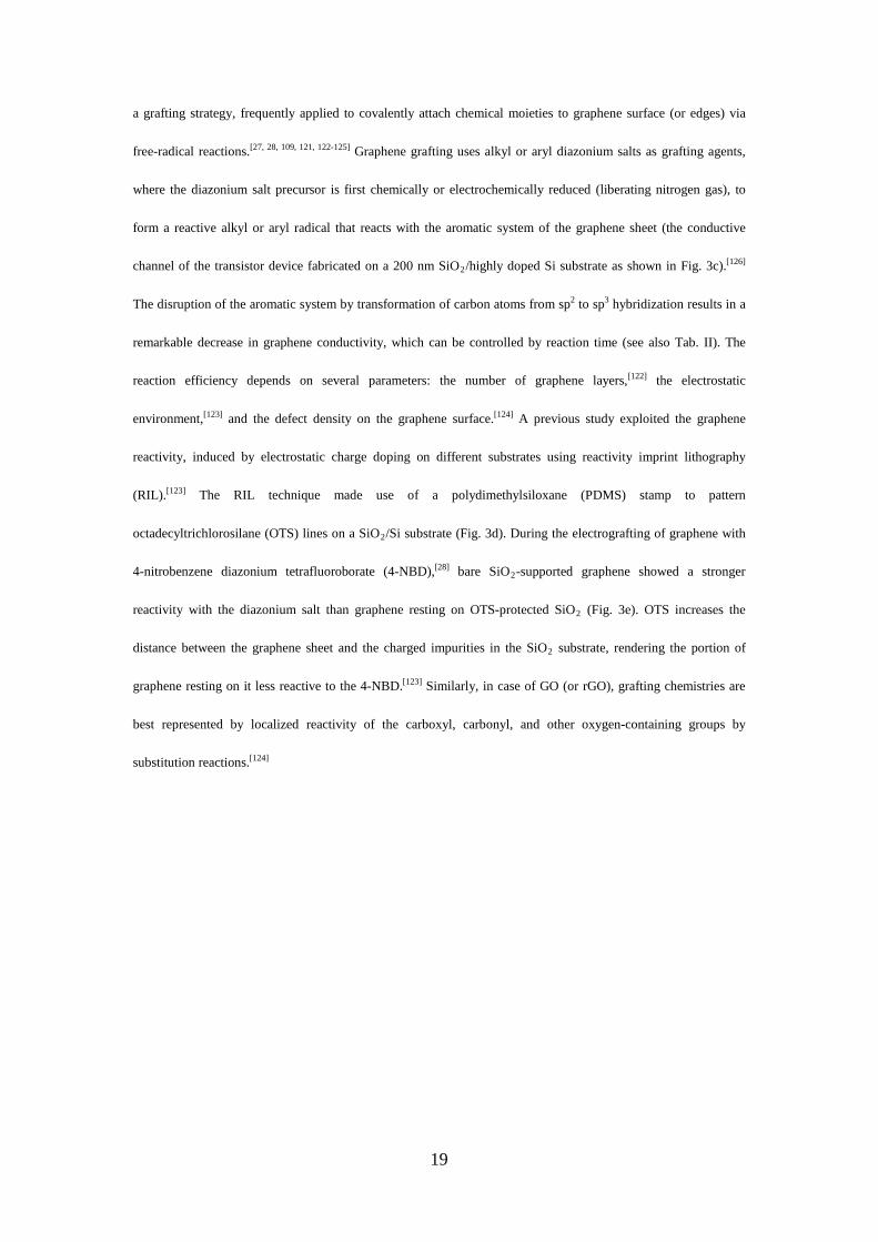
a grafting strategy, frequently applied to covalently attach chemical moieties to graphene surface (or edges) via
free-radical reactions.[27, 28, 109, 121, 122-125] Graphene grafting uses alkyl or aryl diazonium salts as grafting agents,
where the diazonium salt precursor is first chemically or electrochemically reduced (liberating nitrogen gas), to
form a reactive alkyl or aryl radical that reacts with the aromatic system of the graphene sheet (the conductive
channel of the transistor device fabricated on a 200 nm SiO2/highly doped Si substrate as shown in Fig. 3c).[126]
The disruption of the aromatic system by transformation of carbon atoms from sp2 to sp3 hybridization results in a
remarkable decrease in graphene conductivity, which can be controlled by reaction time (see also Tab. II). The
reaction efficiency depends on several parameters: the number of graphene layers,[122] the electrostatic
environment,[123] and the defect density on the graphene surface.[124] A previous study exploited the graphene
reactivity, induced by electrostatic charge doping on different substrates using reactivity imprint lithography
(RIL).[123] The RIL technique made use of a polydimethylsiloxane (PDMS) stamp to pattern
octadecyltrichlorosilane (OTS) lines on a SiO2/Si substrate (Fig. 3d). During the electrografting of graphene with
4-nitrobenzene diazonium tetrafluoroborate (4-NBD),[28] bare SiO2-supported graphene showed a stronger
reactivity with the diazonium salt than graphene resting on OTS-protected SiO2 (Fig. 3e). OTS increases the
distance between the graphene sheet and the charged impurities in the SiO2 substrate, rendering the portion of
graphene resting on it less reactive to the 4-NBD.[123] Similarly, in case of GO (or rGO), grafting chemistries are
best represented by localized reactivity of the carboxyl, carbonyl, and other oxygen-containing groups by
substitution reactions.[124]
20
Fig. 3 Surface chemical functionalizations of graphene materials. (a) Graphene layer (in green) is attacked by cold plasma
hydrogen atoms to produce graphane. (b) Bioconjugation of PEGylated GO with antibody. (c) Schematic of the chemical
functionalization of a GFET devices with 4-nitrobenzene diazonium tetrafluoroborate (4-NBD). (d) AFM image of
octadecyltrichlorosilane (OTS) lines patterned on SiO2 surface. (e) Raman mapping of ID/IG for graphene after 4-NBD reactions:
10mM 4-NBD in aqueous solution with 0.5 wt% sodium dodecyl sulfate (SDS) at 35oC for 1.5 h. (f) STM image of a self-
assembled monolayer of an aromatic molecule (perylene-3,4,9,10-tetracarboxylic-3,4,9,10-dianhydride, PTCDA) (gas-phase
deposition) on a graphene surface (scale bar is 3 nm). Upper panel: molecular structure of PTCDA. (g) Left panel: AFM of
highly oriented pyrolitic graphite (HOPG) incubated for 5 min with a solution of 3 M KCl and 8 M urea and rinsed with
ultrapure water (scale bar is 200 nm). Right panel: HOPG incubated for 5 min with single-stranded M13 DNA (10 ng μl−1) in the
same buffer (scale bar is 200 nm). (h) AFM topographic image of graphene before (left panel) and after (right panel) incubation
with the peptide. Reprinted with permission.
antibody(b)
(d) (e)
(f) (g)
(h)
before
SiO2
Pyr-NHCO-EG4 + DNA DNA
(a) (c)
graphane
graphene
hydrogen atom
graphene
21
3.2. Non-covalent functionalizations
As mentioned in the previous section, non-covalent functionalization has the major advantage of fully preserving
the graphene lattice (i.e., the aromaticity), and thus the electrical performances (see Tab. II). In addition, non-
covalent bond can also be quite strong. For example, the π-π interactions of graphene-benzene and naphthalene
result in a considerable binding energy of almost 0.1 eV per carbon atom; consistently, the binding energy of
graphene-TTP (tetraphenylporphyrin) was calculated to be 3.2 eV, i.e., ~90 % of a typical C-C covalent binding
energy (~3.6 eV).[127] Given the aforementioned advantages, it is a common approach to anchor a biomolecule
onto the graphene surface using an aromatic linker group via non-covalent bonds with excellent sensing
performance in aqueous solutions.[109] Still, we would like to note here that non-covalent functionalizations are
expected to be less compatible with long term usage, at least if compared to stronger covalent functionalizations
(although the covalent modifications of graphene inevitably lead to a severe degradation in the electrical
properties). Nevertheless, non-covalent functionalizations could also be an asset if the sensor surface has to be
regenerated, for example, for recycling the sensor devices.
In general, non-covalent graphene functionalization approaches can be classified based on their corresponding
intermolecular interactions, including π-π or hydrophobic stacking, electrostatic interaction, and van der Waals
interaction as also shown in Tab. I.[109] The self-assembly process of these molecules on the surface of graphene
could be highly controlled and accurately characterized in favor of an actual sensor design.[109, 110] For example,
Fig. 3f shows a scanning tunneling microscopy (STM) image of well-ordered aromatic perylene-3,4,9,10-
tetracarboxylic-3,4,9,10-dianhydride (PTCDA) molecules on graphene (as indicated by the a and b vectors), where
π-π interaction are the driving force of the self-assembly.[92] The perylene-based monolayer is stable and robust
even when exposed to ambient conditions. π-π or hydrophobic interactions between aromatic surface and nucleic
acid moieties can also facilitate the decoration of graphene surface with single-stranded DNA (ssDNA) as shown
in Fig. 3g (right panel, highly oriented pyrolytic graphite (HOPG) was applied in this case).[128] This strong non-
specific ssDNA adsorption can be avoided by first self-assembling a monolayer of pyrene ethylene glycol, thus
rendering the surface of graphene hydrophilic and preventing ssDNA adsorption via hydrophobic interactions (left
panel, Fig. 3g). Besides DNA, proteins[102] or peptides[30, 31] containing aromatic moieties could also self-assemble
on a graphene scaffold. As illustrated in Fig. 3h, the incubation of graphene with the peptides resulted in the
22
formation of an uniform mesh-like layer whilst silicon oxide surface was unaffected. This indicates that the
adsorption occurred specifically on graphene.[31]
Electrostatic interaction is another driving force of the non-covalent assembly. For instance, voltage-biased
graphene can act as an electrophoretic electrode for immobilization of charged biomolecules. The subsequent
detection of complementary analysts can be achieved by using the same graphene transistor devices.[22, 96, 129]
As suggested by Geim and co-workers,[108] weak van der Waals-like interaction between layers could be
exploited to sandwich (a process called ‘encapsulation’) graphene with other 2D layers of, e.g. MoS2, mica, or
hexagonal boron nitride (h-BN). This innovative technique allows the formation of unprecedented multilayer
heterostructures that may be used in devices with adjustable and astonishing electronic properties. For example, by
encapsulating graphene in a h-BN stacking layer, researchers managed to obtain very high electric performances
GFETs, including an exceptionally high carrier mobility of 140,000 cm2/Vs at room temperature, which is close to
the theoretical limit as imposed by acoustic phonon scattering. This extremely high mobility could be ascribed to
very clean interfaces above and below graphene and effective screening of all the defects.[17] Very recently, even
higher mobilities, up to a staggering 197,600 cm2/Vs[52] and 350,000 cm2/Vs[61], have been observed for hBN-
sandwiched graphene samples. One could also explore various 2D crystals as active sensing elements, MoS2 or h-
BN capped MoS2,[53, 130] for instance. Please note that even in a stack such as encapsulated graphene, the
encapsulating layers can be functionalized in the quest of sensing (with the requirement that the encapsulating
layer is sufficiently thin).
As previously discussed, chemical functionalization is essential for unlocking the sensing potential of graphene
surface, but important is also to realize that chemical functionalization also plays a critical role in passivating the
surface of graphene. Surface passivation against unwanted non-specific binding (pyrene ethylene glycol to prevent
any hydrophobic interactions,[128] for example) is crucial to achieve very low detection limits in the presence of
high ionic background levels and to avoid false positives when complex biological samples are assayed.[131]
Importantly, the transfer of large and clean (and crack- and fold-free) graphene sheets is still a critical challenge.
Long chain polymers including poly(methyl methacrylate) (PMMA) – conventionally used for transferring two-
dimensional materials – irreversibly adsorb on the graphene surface, yielding a range of contaminations with
unwanted chemical functions.[132] It is therefore a necessity to take into account the influences of these possible
23
polymer residues as they imped the functionalization of the graphene surface (which is actually not always
discussed, nor clarified in the literature). There is therefore also a large demand for decent polymer-free transfer
methods.[133]
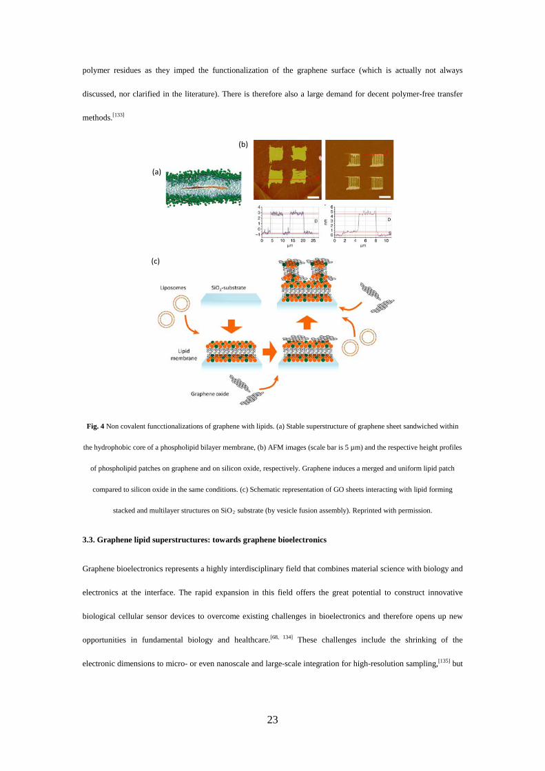
Fig. 4 Non covalent funcctionalizations of graphene with lipids. (a) Stable superstructure of graphene sheet sandwiched within
the hydrophobic core of a phospholipid bilayer membrane, (b) AFM images (scale bar is 5 µm) and the respective height profiles
of phospholipid patches on graphene and on silicon oxide, respectively. Graphene induces a merged and uniform lipid patch
compared to silicon oxide in the same conditions. (c) Schematic representation of GO sheets interacting with lipid forming
stacked and multilayer structures on SiO2 substrate (by vesicle fusion assembly). Reprinted with permission.
3.3. Graphene lipid superstructures: towards graphene bioelectronics
Graphene bioelectronics represents a highly interdisciplinary field that combines material science with biology and
electronics at the interface. The rapid expansion in this field offers the great potential to construct innovative
biological cellular sensor devices to overcome existing challenges in bioelectronics and therefore opens up new
opportunities in fundamental biology and healthcare.[68, 134] These challenges include the shrinking of the
electronic dimensions to micro- or even nanoscale and large-scale integration for high-resolution sampling,[135] but
(a)
(b)
(c)
24
particularly, a complex but well-defined biocompatible interface between graphene surface and cell is at the core
of graphene bioelectronics.
Lipids, as major constituents of the cell membrane, provide a physical barrier between the interior and the
exterior of a cell. Along with their associated proteins, lipids are responsible for the key functions of a cell such as
the highly controlled selectivity of passage of molecules and ions.[136] Despite the hitherto limited knowledge on
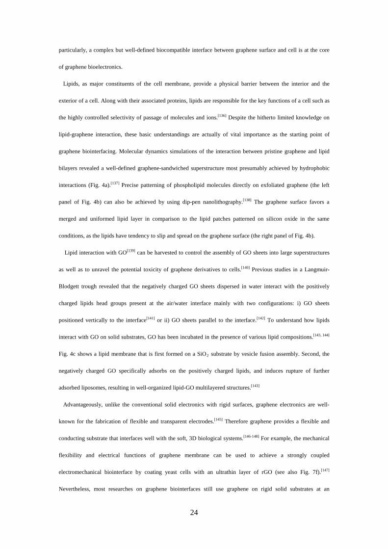
lipid-graphene interaction, these basic understandings are actually of vital importance as the starting point of
graphene biointerfacing. Molecular dynamics simulations of the interaction between pristine graphene and lipid
bilayers revealed a well-defined graphene-sandwiched superstructure most presumably achieved by hydrophobic
interactions (Fig. 4a).[137] Precise patterning of phospholipid molecules directly on exfoliated graphene (the left
panel of Fig. 4b) can also be achieved by using dip-pen nanolithography.[138] The graphene surface favors a
merged and uniformed lipid layer in comparison to the lipid patches patterned on silicon oxide in the same
conditions, as the lipids have tendency to slip and spread on the graphene surface (the right panel of Fig. 4b).
Lipid interaction with GO[139] can be harvested to control the assembly of GO sheets into large superstructures
as well as to unravel the potential toxicity of graphene derivatives to cells.[140] Previous studies in a Langmuir-
Blodgett trough revealed that the negatively charged GO sheets dispersed in water interact with the positively
charged lipids head groups present at the air/water interface mainly with two configurations: i) GO sheets
positioned vertically to the interface[141] or ii) GO sheets parallel to the interface.[142] To understand how lipids
interact with GO on solid substrates, GO has been incubated in the presence of various lipid compositions.[143, 144]
Fig. 4c shows a lipid membrane that is first formed on a SiO2 substrate by vesicle fusion assembly. Second, the
negatively charged GO specifically adsorbs on the positively charged lipids, and induces rupture of further
adsorbed liposomes, resulting in well-organized lipid-GO multilayered structures.[143]
Advantageously, unlike the conventional solid electronics with rigid surfaces, graphene electronics are well-
known for the fabrication of flexible and transparent electrodes.[145] Therefore graphene provides a flexible and
conducting substrate that interfaces well with the soft, 3D biological systems.[146-148] For example, the mechanical
flexibility and electrical functions of graphene membrane can be used to achieve a strongly coupled
electromechanical biointerface by coating yeast cells with an ultrathin layer of rGO (see also Fig. 7f).[147]
Nevertheless, most researches on graphene biointerfaces still use graphene on rigid solid substrates at an
25
intermediate stage mainly focusing on understanding the complicated sensing mechanisms (as the reconfiguration
of the fluidic-like lipid layer has to be considered).[149, 150, 151] For example, a gram-negative bacteria biomimetic
membrane was deposited on CVD GFETs (fabricated on a SiO2/Si substrate) for detecting magainin 2, an
antimicrobial agent. The presence of magainin 2 disrupts and thins the lipid membrane from a thickness of ~5 nm
to ~3 nm.[150] This change in membrane thickness and integrity lead to a significant change in the liquid gate
coupling, and thus to a noticeable field effect which could be measured by the GFETs. The self-assembly
processes of charged lipid bilayers can also induce a sensing signal in the GFET due to surface charge aggregation.
Such GFETs interfaced with biomimetic membrane can even provide enough sensitivity to investigate individual
ion channel activity during the insertion of a pore-forming membrane protein.[151] Graphene bioelectronics for
cellular sensors will be further discussed in the next Section 4.3.
4. Current trends & efforts in biochemical sensing at the surface of GFETs
There has been a vast interest of industry, society, and scientific community in applying graphene materials for
biochemical sensing applications, for portable point-of-care devices for remote diagnostics, for environmental
monitoring, and even for DNA sequencing technologies, etc.[65-67] The outcomes of researches in this area,
however, did not reached the marked yet,[152] although ultimate single molecule sensitivity has been demonstrated
and prototype biosensor chips in various forms have also been developed.[65-67] In the following sections, we will
critically review the current trends in the development of GFET-based gas and ion sensors, protein and DNA
sensors, and cellular sensors in revisiting the ambiguous cases and in meeting the social/scientific needs. A brief
introduction to the graphene electrochemical sensors will also be given as their operation and sensing mechanism
can be regarded to be complementary to GFET sensing technologies.[153, 154] Before discussing the separated cases,
we summarized the sensing performances (and the electrical properties) of GFETs in Tab. III for a selected lists of
frequently reported analytes.
26
Tab. III. Sensing performances of GFETs for a selected list of frequently reported analytes
Analyte Graphene device mobility (cm2/Vs)
Detection limit
Corresponding sensing response |ΔI/I*100%| or |ΔR/R*100%|
Refs (comments)
Gas NO 2 - 1 ppm 0.99 % [155] rGO
~10 20 ppm 21 % [156] CVD
~5,000 1 ppm ~4 % (noise level: ~0.1 %)
[157] Exfoliation
NH 3 - 200 ppm 10.2 % [155] rGO
~10 550 ppm 10 % [156] CVD
~5,000 1 ppm ~4 % (noise level: ~0.1 %)
[157] Exfoliation
5,500 103 ppm 1.5 % [158] Exfoliation, annealed Ion
H+ - 0.67pH 27.8 % [159] rGO - 0.34pH 18 % [160] CVD 3060 - - [161] Exfoliation 4400 0.21pH 8.7 % [162] Exfoliation 5000 0.21pH 12.8 % [163] Exfoliation
K+ ~300 100 μM 40 mV/decadea [37] CVD - 10 nM 7.8 mV/decadea [164] Exfoliation
Na+ - 1 nM 1.5 mV/decadea [165] Exfoliation Ca2+ - 1 μM ~4 % (SNR: 20-30) [166] rGO Cd2+ - 1 nM ~1 % (SNR: 15-20) Hg2+ - 1 nM ~2 % (SNR: 25-30)
~4000 10 ppm (back gate voltage shift: ~6.2 V)
[167] Exfoliation
Pb2+ - 37.5 ng/L (liquid gate voltage shift: ~35mV)
[168] Exfoliation
DNA ssDNA (20-mer) 0.068 0.175 mM 71 % [99] GO ssDNA (33-mer) - 48 nM
(2.4 nM calc. @ SNR=3)
0.6 % (SNR: 60)
[169] rGO
Fully complementary ssDNA (12-mer)
~150-700 0.001 nM ~30 % (in carrier density)
[101] CVD
0.01 nM ~12 % (in mobility) 1-base mismatched ssDNA (12-mer)
0.001 nM - 0.01 nM 0 % (in mobility)
Protein Protective antigen (Anthrax toxin)
- 1.2 aM 1.5 % (@12 aM) [170] rGO
Bovine serum albumin (BSA)
~1250-1750 300 pM ~0.36 % [162] Exfoliation
Immunoglobulin E (IgE)
- 290 pM ~0.3 % [171] Exfoliation
Glucose Glucose - 1 nM 64 % [172] rGO 2298 1.25 mM ~25 % [173] CVD - 30 nM ~1.1 % [174] CVD - 0.5 µM ~ 0.5 % [175] CVD
Cell Embryonic chicken cardiomyocyte cell
4000 ~3.5 mV (SNR ≥4) [176] Exfoliationb
HL-1 mouse atrial tumor cell
3000 100 µV (SNR >10) [177] CVD
a mV/decade: liquid gate voltage shift in the Dirac point of a GFET per decade (ion concentration). b in combination with Si-nanowire device.
As we pointed out in the previous Sections 2.2 and 2.3, it is preferential to use high mobility graphene for
sensing applications as: 1. a higher mobility implies a larger sensing response; 2. a higher mobility complies with
less defects and surface contaminations, which is in favor of an improved noise performance. Such trend is
evidenced, for example, in case of gas sensors. Tab. III showed that for gas detection of both NO2 and NH3,
exfoliated graphene with high mobility (~5000 cm2/Vs) generally demonstrated a much better detection limit ~1
ppm compared to ~1 – 550 ppm of CVD or rGO with lower mobilities. We may also relate the decrease in the
detection limit of DNA molecules – from ~0.001 – 0.01 nM (CVD graphene) to ~48 nM (rGO), and to ~0.175 mM
(GO) – to the degradation in the electrical properties of (functionalized) graphene. In our listed cases of DNA
27
detection, we made the comparisons as all the sensing reactions were based on short chain DNA hybridization, and
thus sharing comparable (at least to a certain extent) bonding constants. We noted here that, it might not always be
fair to make such comparisons, precautions have to be taken as surface condition (functionalization) of graphene
as well as the device geometry might be different from sample to sample (and is not always reported in the
literature). For example, Tab. III showed that annealing exfoliated graphene exhibited a comparable carrier
mobility to as-fabricated exfoliated graphene (from ~5000 cm2/Vs to ~5500 cm2/Vs), but also a strikingly
decreased sensitivity to NH3 gas (from ~1 ppm to ~1000 ppm) due to mainly the different in their surface
conditions (see the following section for detailed discussions).
4.1. GFET gas and ion sensors
The very first chemical sensors fabricated using pristine mechanically exfoliated graphene flakes (Fig. 5a) have
shown very high sensitivity, down even to single molecule detection for the chemisorbed gaseous NO2 (and a
detection limit higher than 1 ppm for NH3 as shown in Fig. 5b, at room temperature).[5] The unprecedented high
sensitivity was explained as a consequence of the extraordinary low intrinsic noise as well as the largest response
of the Hall geometry around the CNP. But this high chemical sensitivity of graphene towards physisorbed gaseous
NH3 is a surprise if considering the fact that graphene is intrinsically chemically inert.[12] Indeed, in more recent
studies, inert electrical responses (i.e., no response) for gaseous NH3 were observed by annealing the exfoliated
graphene at high temperature (400 °C) in Ar/H2 atmosphere to remove possible polymer contaminations and
produce atomically clean graphene sheets.[178] This inert sensing behavior of the cleaned graphene sensors is robust
even upon the exposure to NH3 vapor at a concentration of 1000 ppm (Fig. 5c)[11] and to
dimethylmethylphosphonate (DMMP) vapor at a concentration of 100 ppm (Fig. 5d).[29] It is now widely accepted
that clean graphene should be inert to the presence of most of the gas molecules, although it is possible to amplify
the more subtle dipole moment of a charge neutral gas molecule by switching it and mixing the modulated dipole
signal in a high frequency setup for detection.[179] The previous observed sensitive responses of pristine graphene
to gas molecules could be, therefore, ascribed to defective sensitivities, due to possible defects or polymer
contaminations introduced during device fabrication. The edge of graphene, also plays a crucial role in the
determination of its physical, electronic and chemical properties and thus in the sensing properties. As an example,
holey rGO could be fabricated by using enzymatic oxidation followed by reduction with hydrazine.[180] Such
28
defective graphene – with abundant edge defects – exhibited a large and selective electronic response toward the
detection of hydrogen, particularly when decorated with Pt nanoparticles.[180] In principle, the substrate surface
conditions are also suspected to influence the edge of graphene, and hence the sensing properties of the GFET
devices especially at nanoscale.[181]
GFET based pH sensors measure the protonation and deprotonation at the (functionalized) graphene surface.
They hold great potentials especially in food industry and medical applications for glass-free pH measurement
requiring the highest level performance, small size, and/or flexibility.[182] In earlier reports, GFET based pH
sensors exhibited large variation in their pH sensitivities, ranging from a low value of 12 mV/pH to a value of 99
mV/pH.[7-10, 21] The latter value is even larger than the thermodynamically allowed maximal shift of 60 mV/pH
(the so-called Nernst value) at room temperature.[8] It became clear later on that the large range of pH-induced gate
shifts observed in the previous literature could be ascribed to defects as well as surface contaminations reflecting
the quality of as-fabricated graphene.[66, 183] Practically GFETs are normally composed of CVD graphene and
contain therefore defects in the lattice introduced during growth.[55] Exfoliated samples are also subject to various
polymer and metal contaminations coming from the fabrication process.[11] These defects and contaminations also
account for the discrepancies reported in earlier literature on pristine graphene chemical sensors.[5-7] Such defect-
induced ionic response can be suppressed by passivating the graphene layer with inert aromatic molecules such as
fluorobenzene.[12] As a consequence of its ideal hydrophobic surface with a very small amount (ideally zero) of
dangling bonds, such a clean GFET should be inert to the change of electrolyte compositions, and could therefore
act as a novel solid-state reference electrode that senses only the electrostatic potential in aqueous electrolytes
unless a chemo-adsorption or a physico-adsorption of charged ions is considered.[184] On the contrary, by
functionalizing the GFETs with active groups, for example, with proton sensitive phenol or K+ sensitive crow
ethers conjugated with aromatic molecular anchor groups, a pH response up to ~49 mV/decade or a K+ ionic
response up to ~40 mV/dec was achieved.[37] An alternative approach is to directly coat an ion-selective membrane
(ISM) on graphene surface. A recent report has demonstrated the selective detection of K+ ions (-8 mV/dec) over
Na+ ions (-0.2 mV/dec) in an electolyte solution with an ISM composed of valinomycin, a K+ selective
ionophore.[185]
29
Fig. 5 (a) Colored SEM of a graphene (purple) Hall bar device. The scale bar is given by the width of the Hall bar, which is 1
μm. Yellow color corresponds to metal electrodes evaporated on the SiO2/Si substrate. (b) Relative changes in resistivity (Δρ/ρ,
in percentage) caused by the exposure of graphene to various gases diluted at 1 ppm (NH3: blue curve, CO: green curve, H2O:
purple curve, NO2: red curve). Here the positive (respectively negative) changes in the Δρ/ρ curves in blue and green (purple and
red, respectively) indicate electron (hole) doping. (c) Relative changes in current (ΔI/I, in percentage) of annealed exfoliated
graphene (1 h at 400 °C in Ar/H2 atmosphere) towards the detection of ammonia vapors. The lower amount of defects in the
clean graphene device yields smaller changes in the sensing response, even for ammonia concentrations as high as 1000 ppm.
Lower arrows indicate when the sensor device was flushed with a pure N2 carrier gas. (d) Relative changes in current (ΔI/I, in
percentage) caused by the exposure of clean graphene device (black data) and ssDNA functionalized graphene devices (Seq1 in
blue: 5´-GAG TCT GTG GAG GAG GTA GTC-3´, Seq2 in red: 5´-CTT CTG TCT TGA TGT TTG TCA AAC-3´) to
dimethylmethylphosphonate (DMMP) vapor at concentrations of 20, 40, 60, 80, 100, and 120 ppm. Upper arrows indicate when
the sensor cell was purged with inert N2 gas. (e) A conceptual nodal architecture of an internet of things consisting of
nanomaterial sensing modulators made of wireless GFET solutions. Reprinted with permission.
(a)
(b)
(d)
(c)
(e)
30
Heavy metals that are notorious to health and environment (e.g. Hg, Cr, Cd, Pb) motivate the current interests in
graphene heavy metal sensors.[186, 187] Scientists have functionalized the surface of exfoliated graphene with a self-
assembled monolayer of 1-octadecanethiol and applied it for Hg2+ sensing.[188] Due to the high binding affinity of
the thiol groups of 1-octadecanethiol to Hg2+, the sensor achieved a detection limit of 10 ppm. DNAzyme aptamer
decoration, on the other hand, leads to Pb2+ detection down to 37.5 ng/L with prototype device demonstrated using
real blood samples.[189] Instead of using exfoliated graphene, solution-processable rGO has also been developed for
a low-cost, scalable fabrication of GFET sensors.[190] By functionalizing the rGO with specific metal ion binding
proteins or gold nanoparticle, nanomolar concentrations of Hg2+, Cd2+, and Pb2+ were detected.[186] Impressive
prospective has also been shared for smart graphene chemical sensors (which can be, in principle, wireless and
wearable[191]) with low maintenance cost and low energy consumption for real-time, event-based monitoring in
pervasive healthcare internet-of-things applications (Fig. 5e).[192] The selectivity of the detection, however, was not
always thoroughly studied or understood in the reports representing a major challenge in the field (and for GFET
biosensors in general).[193]
4.2. GFET glucose, DNA and protein biosensors
Glucose detection has been an enduring topic since it directly reflects the metabolism condition and inspection of
the chronic diabetes (the physiological concentration range of glucose detection falls in ~2-20 mM in serum).[194,
195] Recently, the perspectives for non-invasive portable point-of-care (POC) glucose sensors imposed imperative
need for biosensors with high sensitivity and reliability, as the glucose levels in body fluids (saliva, tears, urine,
etc.) are much lower (~0.01 %) than that in plasma.[196] Conventional electrochemical glucose sensors are not
sensitive enough for these applications. On the other hand, detection of glucose with the aid of electronic devices
such as GFETs can reach high sensitivity down to nM concentrations (see Tab. II), which are sensitive enough for
non-invasive glucose detections in body fluids. It is noteworthy that GFET glucose biosensors has also been
fabricated on flexible supports such as PET (Polyethylene terephthalate)[197] and silk fibroin[198]. As a continuous
effort to achieve flexible and cheap biosensors, recently a GFET was implemented within an 2D paper network for
practical glucose detection (~1.25 mM).[199] Interestingly, using a PANI/Nafion-bilayer graphene modified gate
electrode, researchers could also determine glucose level in saliva with a detection limit of 30 nM.[200] We would
like to note here that, despite the recent achievements in GFET glucose biosensor development, more researches
31
are still needed to achieve a highly sensitive and reliable platform for home use or portable application. These
challenges include modifying enzyme activity for improved performance, developing methods to reliably bind
them to the graphene surface, and incorporating the (functionalized) GFET into a microfluidic device.[194]
Intrinsically, many DNAs and proteins, which contain aromatic groups, can bind onto graphene surface through
π–π interaction or simply by hydrophobic interactions (see Tab. I).[98] In one of the first GFET DNA sensors,
single-stranded DNA (ssDNA) was anchored on the surface of GFETs and used to detect complementary DNA
strands through hybridization.[99] It has also been demonstrated that the GFETs were capable of detecting DNA
hybridizations with single-base specificity.[201] One step further from a single device to multiplexed DNA arrays,
CVD GFET sensor arrays were manufactured (Fig. 6a) and acted as both an electrophoretic electrode for site-
specific DNA immobilization (not shown here) and hybridization detection down to 100 fM (Fig. 6b).[22] GFETs
were also capable of distinguishing the conductance signature upon adsorption of the four different DNA
nucleobases due to the different interface dipole field.[97] The same study concluded that the sensing of single
nucleotide with graphene is feasible even without DNA amplification (amplification of DNA showed a detection
limit of 50 aM using Rolling Circle Amplification[100]). Another possibility for graphene-based DNA sensors,[202]
is to configure a graphene nanoribbon FET with a nanopore and to probe the subtle differences in the conductance
as the negatively charged DNA molecules translocating through the nanopore.[203] Interestingly, single-stranded
DNA can also be used as a sensitizing agent to selectively probe various gases.[29] Contrarily to the inert sensing
behavior of clean GFETs to various gas vapor such as dimethylmethylphosphonate (DMMP, black line, Fig. 5d),
ssDNA decorated GFET showed selective sensing responses to vapor of DMMP (blue and red lines indicate
different sensing responses when the GFETs were functionalized with two DNA sequences).[29] We note here that,
as a functional DNA or RNA molecule selected in vitro to bind pre-selected analytes (organic and inorganic
molecules and proteins) with high affinity and specificity, aptamers also represent a versatile toolbox for
producing novel graphene sensors.[171, 204, 205]
32
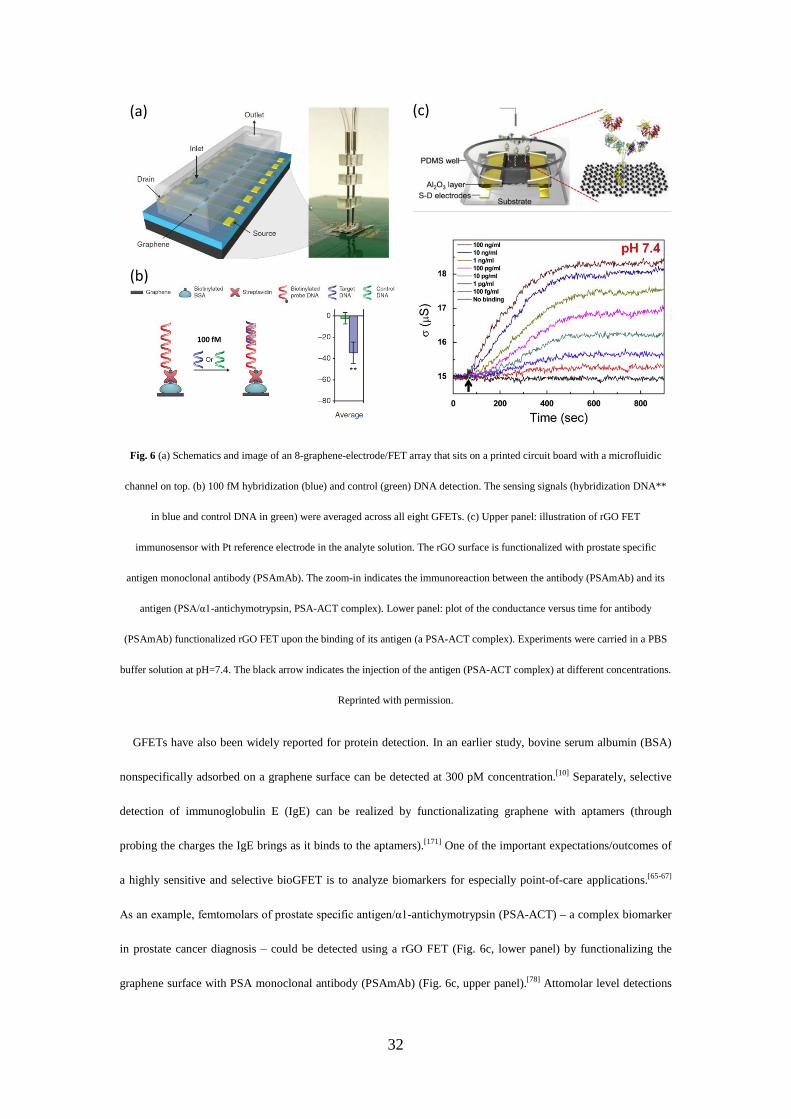
Fig. 6 (a) Schematics and image of an 8-graphene-electrode/FET array that sits on a printed circuit board with a microfluidic
channel on top. (b) 100 fM hybridization (blue) and control (green) DNA detection. The sensing signals (hybridization DNA**
in blue and control DNA in green) were averaged across all eight GFETs. (c) Upper panel: illustration of rGO FET
immunosensor with Pt reference electrode in the analyte solution. The rGO surface is functionalized with prostate specific
antigen monoclonal antibody (PSAmAb). The zoom-in indicates the immunoreaction between the antibody (PSAmAb) and its
antigen (PSA/α1-antichymotrypsin, PSA-ACT complex). Lower panel: plot of the conductance versus time for antibody
(PSAmAb) functionalized rGO FET upon the binding of its antigen (a PSA-ACT complex). Experiments were carried in a PBS
buffer solution at pH=7.4. The black arrow indicates the injection of the antigen (PSA-ACT complex) at different concentrations.
Reprinted with permission.
GFETs have also been widely reported for protein detection. In an earlier study, bovine serum albumin (BSA)
nonspecifically adsorbed on a graphene surface can be detected at 300 pM concentration.[10] Separately, selective
detection of immunoglobulin E (IgE) can be realized by functionalizating graphene with aptamers (through
probing the charges the IgE brings as it binds to the aptamers).[171] One of the important expectations/outcomes of
a highly sensitive and selective bioGFET is to analyze biomarkers for especially point-of-care applications.[65-67]
As an example, femtomolars of prostate specific antigen/α1-antichymotrypsin (PSA-ACT) – a complex biomarker
in prostate cancer diagnosis – could be detected using a rGO FET (Fig. 6c, lower panel) by functionalizing the
graphene surface with PSA monoclonal antibody (PSAmAb) (Fig. 6c, upper panel).[78] Attomolar level detections
(a)
(b)
(c)
100 fM
33
have also been reported occasionally[205] but such significantly improved sensitivities were not always consistent
with the more generally observed nM-pM detection limit,[66, 67] suggesting that more dedicated efforts are still
needed to improve the reliability and the reproducibility of the sensing response.[206] This brings us back to some
of the fundamental issues associated with graphene-based BioFETs (and BioFETs in general) as eventually, after
carefully designing and controlling every steps of a GFET, we will be looking at the Debye screening effects as an
obstacle to achieve ultimate detection of a relatively large biomolecule in physiological conditions as previously
discussed in Section 2.5 and will be further reviewed in the next Section 5.2. Alternatively, the detection of
biomolecules can also be achieved by monitoring pH changes during adsorption, thus circumventing the Debye
screening effects as proton is negligibly small.[207] Along this line, GFETs were applied as pH sensors to detect
alanine aminotransferase (ALT) in the concentration range of 10-100 unit/L by monitoring the generation of
protons during the enzymatic reaction between L-alanine/α-ketoglutarate and ALT.[208]
4.3. GFET biological cellular sensors
Recently, as a part of the Europe’s Graphene Flagship – a €1 billion project aims to bring graphene from
innovative laboratory researches into commercial applications, scientists interfaced graphene to neurons directly,
while retaining the integrity of these vital nerve cells.[148] In fact, stimulating and recording extracellular potentials
(or even intracellular potential using branched transistors[209]) from neurons is one of the hallmark of modern
bioelectronics. Graphene can serve not only as conductive electrodes to transduce stimuli into the cells, but also as
the conductive channel of GFETs to monitor the presence and activity of the cells.[99] Fig. 7a illustrates a cell-
transistor measurement,[68] where a cell is located on the graphene surface. A constant bias voltage is applied to the
drain and source electrodes (in gold yellow), bridged by a graphene conductive channel (in pink). The current in
the graphene channel is amplified and monitored in real time. Any local electrochemical potential change triggered
by the action potential of the cell leads to a modulation of the source-drain current in graphene (due to the field
effect). A separate study combined GFETs (exfoliated graphene) and silicon nanowire FETs to probe single
electrogenic cardiomyocyte cell (Fig. 7b).[176] The GFETs yielded well-defined current peaks (extracellular signals)
with signal-to-noise ratio (SNR) routinely above four, which is comparable to that of the nanowire FETs (Fig.
7c).[176] Narrow GFETs (~2 um×3 um) exhibit similar peak-to-peak widths as the nanowireFET (~100 times
smaller per area). But GFET devices with large size (~20 um×10 um) detect an average of the extracellular
34
potential from beating cells and yield a broadened peak-to-peak signal width.
Arrays of GFET have been developed to monitor tissue-like specimens.[210] Densely packed cardiomyocyte-like
HL-1 cells were cultured on the surface of graphene arrays (a fluorescence image of the cells is shown in Fig. 7d).
The propagation of the action potentials across the beating cellular network is monitored by recording the current
flowing through the transistor array (Fig. 7e). In the current trace, spikes from the different GFETs depict the
variations in the graphene-cell coupling and the propagation of the action potentials across the HL-1 cell network.
Furthermore, these GFETs exhibit a SNR better than ten. Even at its early stage of development, such SNR
performance equals (or even surpasses) that of well-established techniques like the microelectrode arrays (MEAs)
and the planarFET[211] and nanowireFET[176].
In order to provide a control over the specific voltage-gated ion-channels in the cell membrane[212] (and thus the
action potential of the cell), patch-clamping experiments were combined with GFETs (Fig. 7a), where a patch
pipette containing an inner electrode was manually introduced into the inner part of a single HEK-293 cell.
Because the HEK-293 cell were genetically modified so that the membrane contains only K+ channels,[213] the
opening and closing of these ion channels could be unambiguously identified by monitoring the current across the
membrane with the patch electrodes.[68] Simultaneously, signals from the GFET could be attributed to these K+
channels and very good SNR (up to fifty) could be achieved by repeating the same process multiple times.[68]
Besides the action potential, GFET can also measure the electromechanical coupling between rGO microsheets
and – for example – yeast cells (Fig. 7f).[147] The flexible rGO layer responses electrically to the change in cell
volume when exposed to different alcohols due to a strong mechanical coupling. By monitoring the dynamic
electrical response of rGO, it was possible to differentiate between ethanol, 2-propanol, and water, each inducing
different physiological stress response on the cell.
Based on the current state-of-the-art of GFET cellular sensors, graphene and graphene-related materials have
confirmed their suitability for monitoring the activity of cells with excellent SNR (both electrically and
mechanically). Looking ahead, new advancements could reside in the development of flexible GFET cellular
sensors,[214] by combining the outstanding electronic performances of GFET with the high flexibility of
graphene.[215] In such a flexible bioelectronic platform, individual cells in a network can be addressed via electrical
interfaces, which could potentially lead to advanced learning circuits, neuron-implants, and neuroprosthesis that
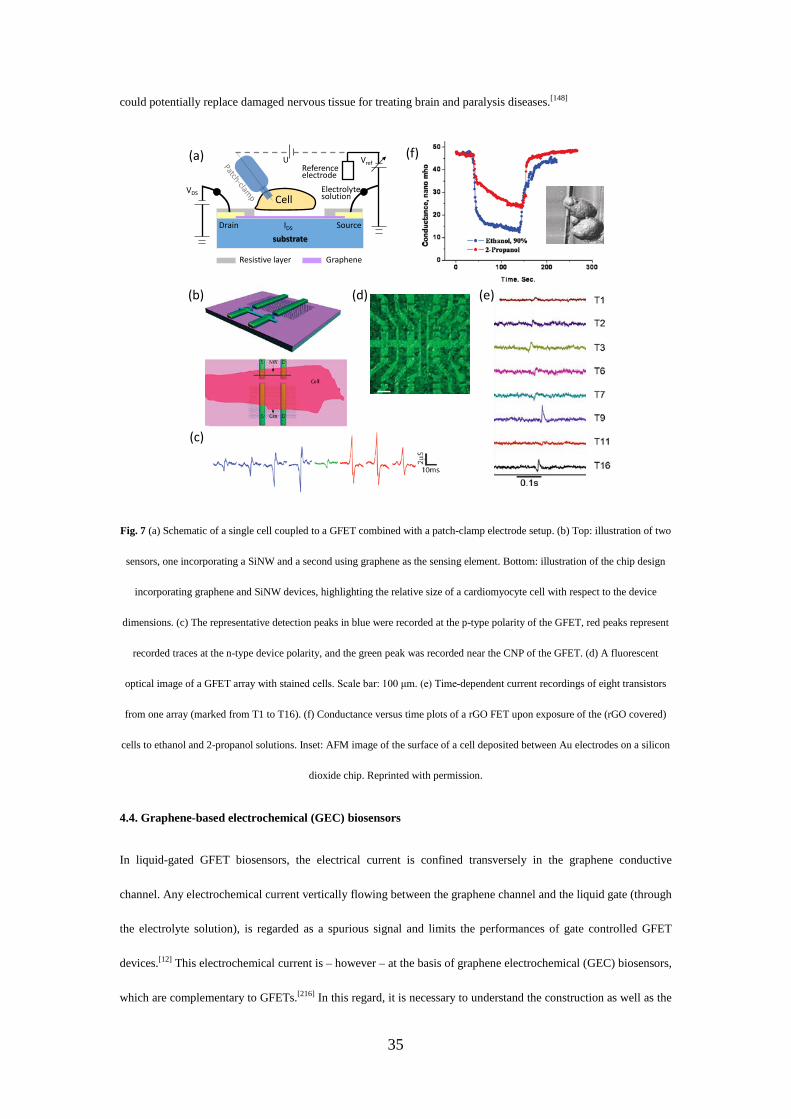
35
could potentially replace damaged nervous tissue for treating brain and paralysis diseases.[148]
Fig. 7 (a) Schematic of a single cell coupled to a GFET combined with a patch-clamp electrode setup. (b) Top: illustration of two
sensors, one incorporating a SiNW and a second using graphene as the sensing element. Bottom: illustration of the chip design
incorporating graphene and SiNW devices, highlighting the relative size of a cardiomyocyte cell with respect to the device
dimensions. (c) The representative detection peaks in blue were recorded at the p-type polarity of the GFET, red peaks represent
recorded traces at the n-type device polarity, and the green peak was recorded near the CNP of the GFET. (d) A fluorescent
optical image of a GFET array with stained cells. Scale bar: 100 μm. (e) Time-dependent current recordings of eight transistors
from one array (marked from T1 to T16). (f) Conductance versus time plots of a rGO FET upon exposure of the (rGO covered)
cells to ethanol and 2-propanol solutions. Inset: AFM image of the surface of a cell deposited between Au electrodes on a silicon
dioxide chip. Reprinted with permission.
4.4. Graphene-based electrochemical (GEC) biosensors
In liquid-gated GFET biosensors, the electrical current is confined transversely in the graphene conductive
channel. Any electrochemical current vertically flowing between the graphene channel and the liquid gate (through
the electrolyte solution), is regarded as a spurious signal and limits the performances of gate controlled GFET
devices.[12] This electrochemical current is – however – at the basis of graphene electrochemical (GEC) biosensors,
which are complementary to GFETs.[216] In this regard, it is necessary to understand the construction as well as the
(f)
(b)
(c)
Resistive layer
Electrolyte solution
VDS
Vref
Graphene
Cell
(a)
substrate
(d) (e)
Drain SourceIDS
Reference electrode
U
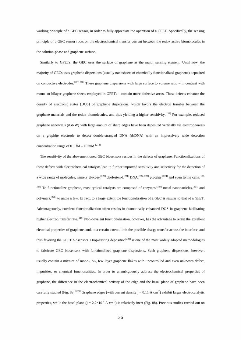
36
working principle of a GEC sensor, in order to fully appreciate the operation of a GFET. Specifically, the sensing
principle of a GEC sensor roots on the electrochemical transfer current between the redox active biomolecules in
the solution-phase and graphene surface.
Similarly to GFETs, the GEC uses the surface of graphene as the major sensing element. Until now, the
majority of GECs uses graphene dispersions (usually nanosheets of chemically functionalized graphene) deposited
on conductive electrodes.[217, 218] These graphene dispersions with large surface to volume ratio – in contrast with
mono- or bilayer graphene sheets employed in GFETs – contain more defective areas. These defects enhance the
density of electronic states (DOS) of graphene dispersions, which favors the electron transfer between the
graphene materials and the redox biomolecules, and thus yielding a higher sensitivity.[219] For example, reduced
graphene nanowalls (rGNW) with large amount of sharp edges have been deposited vertically via electrophoresis
on a graphite electrode to detect double-stranded DNA (dsDNA) with an impressively wide detection
concentration range of 0.1 fM – 10 mM.[218]
The sensitivity of the abovementioned GEC biosensors resides in the defects of graphene. Functionalizations of
these defects with electrochemical catalysts lead to further improved sensitivity and selectivity for the detection of
a wide range of molecules, namely glucose,[220] cholesterol,[221] DNA,[222, 223] proteins,[224] and even living cells.[103,
225] To functionalize graphene, most typical catalysts are composed of enzymes,[226] metal nanoparticles,[227] and
polymers,[228] to name a few. In fact, to a large extent the functionalization of a GEC is similar to that of a GFET.
Advantageously, covalent functionalization often results in dramatically enhanced DOS in graphene facilitating
higher electron transfer rate.[219] Non-covalent functionalization, however, has the advantage to retain the excellent
electrical properties of graphene, and, to a certain extent, limit the possible charge transfer across the interface, and
thus favoring the GFET biosensors. Drop-casting deposition[223] is one of the most widely adopted methodologies
to fabricate GEC biosensors with functionalized graphene dispersions. Such graphene dispersions, however,
usually contain a mixture of mono-, bi-, few layer graphene flakes with uncontrolled and even unknown defect,
impurities, or chemical functionalities. In order to unambiguously address the electrochemical properties of
graphene, the difference in the electrochemical activity of the edge and the basal plane of graphene have been
carefully studied (Fig. 8a).[229] Graphene edges (with current density j = 0.11 A cm-2) exhibit larger electrocatalytic
properties, while the basal plane (j = 2.2×10⁻⁴ A cm-2) is relatively inert (Fig. 8b). Previous studies carried out on
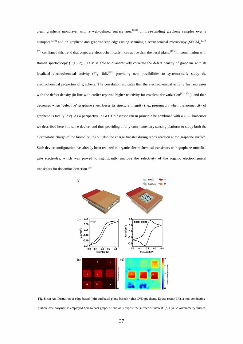
37
clean graphene monolayer with a well-defined surface area,[230] on free-standing graphene samples over a
nanopore,[231] and on graphene and graphite step edges using scanning electrochemical microscopy (SECM),[232,
233] confirmed this trend that edges are electrochemically more active than the basal plane.[125] In combination with
Raman spectroscopy (Fig. 8c), SECM is able to quantitatively correlate the defect density of graphene with its
localized electrochemical activity (Fig. 8d),[233] providing new possibilities to systematically study the
electrochemical properties of graphene. The correlation indicates that the electrochemical activity first increases
with the defect density (in line with earlier reported higher reactivity for covalent derivatization[122, 234]), and then
decreases when ‘defective’ graphene sheet losses its structure integrity (i.e., presumably when the aromaticity of
graphene is totally lost). As a perspective, a GFET biosensor can in principle be combined with a GEC biosensor
we described here in a same device, and thus providing a fully complementary sensing platform to study both the
electrostatic charge of the biomolecules but also the charge transfer during redox reaction at the graphene surface.
Such device configuration has already been realized in organic electrochemical transistors with graphene-modified
gate electrodes, which was proved to significantly improve the selectivity of the organic electrochemical
transistors for dopamine detection.[154]
Fig. 8 (a) An illustration of edge-based (left) and basal plane-based (right) CVD graphene. Epoxy resin (ER), a non-conducting
pinhole-free polymer, is employed here to coat graphene and only expose the surface of interest. (b) Cyclic voltammetry studies
(c) (d)
(a)
(b) edge basal plane
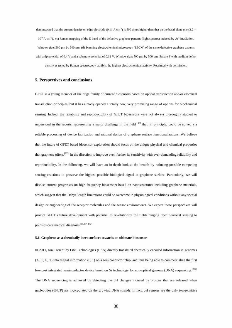
38
demonstrated that the current density on edge electrode (0.11 A cm-2) is 500 times higher than that on the basal plane one (2.2 ×
10-4 A cm-2). (c) Raman mapping of the D band of the defective graphene patterns (light squares) induced by Ar+ irradiation.
Window size: 500 µm by 500 µm. (d) Scanning electrochemical microscopy (SECM) of the same defective graphene patterns
with a tip potential of 0.4 V and a substrate potential of 0.11 V. Window size: 500 µm by 500 µm. Square F with medium defect
density as tested by Raman spectroscopy exhibits the highest electrochemical activity. Reprinted with permission.
5. Perspectives and conclusions
GFET is a young member of the huge family of current biosensors based on optical transduction and/or electrical
transduction principles, but it has already opened a totally new, very promising range of options for biochemical
sensing. Indeed, the reliability and reproducibility of GFET biosensors were not always thoroughly studied or
understood in the reports, representing a major challenge in the field[193] that, in principle, could be solved via
reliable processing of device fabrication and rational design of graphene surface functionalizations. We believe
that the future of GFET based biosensor exploration should focus on the unique physical and chemical properties
that graphene offers,[235] in the direction to improve even further its sensitivity with ever-demanding reliability and
reproducibility. In the following, we will have an in-depth look at the benefit by reducing possible competing
sensing reactions to preserve the highest possible biological signal at graphene surface. Particularly, we will
discuss current progresses on high frequency biosensors based on nanostructures including graphene materials,
which suggest that the Debye length limitations could be overcome in physiological conditions without any special
design or engineering of the receptor molecules and the sensor environments. We expect these perspectives will
prompt GFET’s future development with potential to revolutionize the fields ranging from neuronal sensing to
point-of-care medical diagnosis.[65-67, 192]
5.1. Graphene as a chemically inert surface: towards an ultimate biosensor
In 2011, Ion Torrent by Life Technologies (USA) directly translated chemically encoded information in genomes
(A, C, G, T) into digital information (0, 1) on a semiconductor chip, and thus being able to commercialize the first
low-cost integrated semiconductor device based on Si technology for non-optical genome (DNA) sequencing.[207]
The DNA sequencing is achieved by detecting the pH changes induced by protons that are released when
nucleotides (dNTP) are incorporated on the growing DNA strands. In fact, pH sensors are the only ion-sensitive
39
FET sensors that have been successfully commercialized due to the highly sensitive (~60 mV/pH) and selective
nature of the highly abundant hydroxyl (–OH) terminal groups on the oxide surface (SiO2, Al2O3, HfO2, Ta2O5,
etc.) towards protons.[42] Although Si ion-sensitive FETs can also probe and detect biomolecules directly,[236] no
commercial biological ion-sensitive FETs has been released so far. In fact: i) such devices are more capable of
detecting small molecules such as protons, as the Debye screening effect limits the charge detection of large
biomolecules (details will be discussed in Section 5); ii) the very high density of the hydroxyl (–OH) groups
diminish the sensing response of the Si ion-sensitive FET to biomolecules. That is, upon the binding of target
biomolecules onto the receptors immobilized on the surface of a Si ion-sensitive FET, the protonation (–OH2+) or
deprotonation (–O-) of the nearby unpassivated –OH groups[42] (a full passivation of the surface –OH groups by
receptors is difficult[237]) will buffer and significantly screen/hinder the sensing response of the Si ion-sensitive
FET to the charged biomolecules.[236] In this regard, beside the above discussed well-known advantages (such as
high mobility, low intrinsic electrical noise, large surface to volume ratio and stability) the fact that graphene
possesses a surface that is free of dangling bonds (–OH groups, for example), represents another significant
advantage and unprecedented opportunities over Si ion-sensitive FETs for biosensing applications.
This screening/interference effect can be understood by considering the following iterative sensing steps: i)
positively charged target biomolecules attaching to the receptors cause a change in the total surface charge: +ΔQ0
(biosensing signal); ii) the change in the total surface charge initiates a redistribution of the proton concentration
near the sensor surface due to Boltzmann distribution in the electrolyte environment;[42] iii) the change in the
proton concentration at the surface will, in turn, induce a negative change in the surface charge -ΔQ01 due to the
protonation/deprotonation of the –OH groups, which will compensate the aforementioned sensing signal +ΔQ0. In
an extreme case, this compensation will be complete if the sensor surface has a Nernstian pH response[238]
(indicating very high density of unpassivated –OH groups). Consequently, there will be no sensing response
because any changes in the surface charge +ΔQ0 due to positively charged target biomolecules attached to surface
immobilized receptors are totally screened by the protonation/deprotonation reactions. In fact, a reduced
biosensing signal can be measured if the compensation is not complete.[239] In our opinions, this screening effect
has caused many problems for FET-type of biosensing applications (sometimes even without noticing), where the
surface functionalization started with a surface of very high –OH group density. In the contrary, the highest
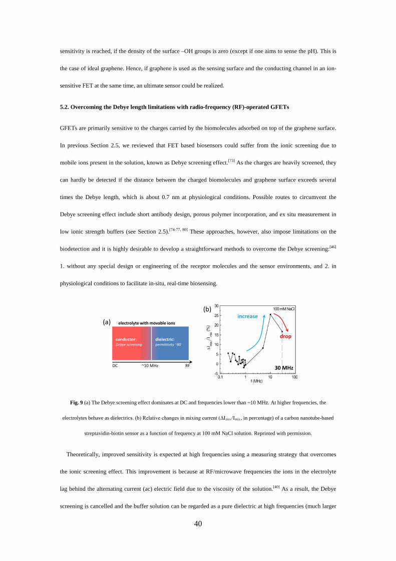
40
sensitivity is reached, if the density of the surface –OH groups is zero (except if one aims to sense the pH). This is
the case of ideal graphene. Hence, if graphene is used as the sensing surface and the conducting channel in an ion-
sensitive FET at the same time, an ultimate sensor could be realized.
5.2. Overcoming the Debye length limitations with radio-frequency (RF)-operated GFETs
GFETs are primarily sensitive to the charges carried by the biomolecules adsorbed on top of the graphene surface.
In previous Section 2.5, we reviewed that FET based biosensors could suffer from the ionic screening due to
mobile ions present in the solution, known as Debye screening effect.[73] As the charges are heavily screened, they
can hardly be detected if the distance between the charged biomolecules and graphene surface exceeds several
times the Debye length, which is about 0.7 nm at physiological conditions. Possible routes to circumvent the
Debye screening effect include short antibody design, porous polymer incorporation, and ex situ measurement in
low ionic strength buffers (see Section 2.5).[74-77, 80] These approaches, however, also impose limitations on the
biodetection and it is highly desirable to develop a straightforward methods to overcome the Debye screening:[46]
1. without any special design or engineering of the receptor molecules and the sensor environments, and 2. in
physiological conditions to facilitate in-situ, real-time biosensing.
Fig. 9 (a) The Debye screening effect dominates at DC and frequencies lower than ~10 MHz. At higher frequencies, the
electrolytes behave as dielectrics. (b) Relative changes in mixing current (ΔImix/Imix, in percentage) of a carbon nanotube-based
streptavidin-biotin sensor as a function of frequency at 100 mM NaCl solution. Reprinted with permission.
Theoretically, improved sensitivity is expected at high frequencies using a measuring strategy that overcomes
the ionic screening effect. This improvement is because at RF/microwave frequencies the ions in the electrolyte
lag behind the alternating current (ac) electric field due to the viscosity of the solution.[40] As a result, the Debye
screening is cancelled and the buffer solution can be regarded as a pure dielectric at high frequencies (much larger
(b)
RF
conductor:Debye screening
dielectric:permittivity ~80
~10 MHzDC
electrolyte with movable ions(a)increase
drop
30 MHz
41
than 10 MHz, see Fig. 9a).[40] And hence the displacement of water from the interface by a lower dielectric
constant such as a biomolecule can be detected/transduced as the output signal of the RF sensors, which ultimately
relates to the chemical structure (i.e., dipole moment) of the biomolecule.[46] Recently, in an attempt to detect
beyond the Debye length, carbon nanotube sensors were operated at frequencies up to ~10 MHz.[46] The sensing
response, defined as the relative change of the measured mixing current ΔImix/Imix of the sensor, increases for
increasing the measurement frequencies (up to 10 MHz, Fig. 9b, blue arrow) due to a continuous reduction of the
Debye screening effect. However, an unexpected drop in the sensing response at 30 MHz was observed (Fig. 9b,
red arrow). In fact, at frequency smaller than 10 MHz the ions in the aqueous solution (at physiological conditions)
can still follow the electrical signal.[40] As a result, the charged biomolecules are still screened (at least partially)
by the movable ions in the buffer solutions (Fig. 9a). In order to unambiguously test whether GFET operated at
high frequency can overcome the Debye screening limitation, further research at frequencies above 10 MHz would
still be highly desired.
In fact, owing to its exceptional high mobilities, graphene is potentially suited for high-frequency
applications.[15] For instance, high-frequency GFETs with an intrinsic cut-off frequency of above 300 GHz have
been demonstrated, which outperforms the best silicon FETs with similar gate lengths.[240] However, our
knowledge of the high-frequency (much higher than 10 MHz) properties of GFETs in the presence of the
electrolyte (in direct contact with the graphene layer) is very limited. As an attempt to forward our understanding
of the RF properties of graphene, especially with regards to sensing in a liquid environment, the operation of an
electrolyte-gated GFET at RF/microwave frequencies (~2-4 GHz) has been achieved in a recent study.[241] Owing
to the wide bandwidth, the graphene RF device also enables ultrafast measurements at nanosecond time-
resolved.[241] We note here that AC electric field also exerts great influences on the fluid and results in micro-nano
electrokinetic phenomena like electroosmosis and especially dielectrophoresis,[242] which could, in principle, be
adopted to manipulate, sort, and concentrate different types of nanoparticles and biomolecules at the strongest field
range to enhance further the detection limit. Indeed, the development of RF sensors is still in the early stage, but
already reveals great potential for a wide range of biochemical sensing applications.[243] Sincerely, we hope that
the perspective of RF graphene biosensors will open up new directions in research in the biomedical,
environmental, and other high performance sensor fields.[192]
42
To conclude, this article comprehensively reviews recent research efforts devoted to understanding the
operation mechanisms of GFETs in electrolytic environments, and to functionalizing the graphene surface with
particular recognition moieties to unlock its sensitivity potential. We provide a timely overview on the recent
developments of gas sensors, protein and DNA biosensors, and biological cellular sensors, using the surface of
graphene as the sensing element. We are convinced that graphene biochemical sensors hold great promise to meet
the increasing demands on the sensitivity, especially by the recent progresses on operating GFETs at high
frequencies suggesting that Debye screening can be overcome.
Acknowledgements
The research leading to this review has gratefully received funding from the European Research Council under the
European Union's Seventh Framework Programme (FP/2007-2013) / ERC Grant Agreement n. 335879 project
acronym ‘Biographene’, the FP7 funded DECATHLON Grant agreement n. 613908 ‘Development of Cost
efficient Advanced DNA-based methods for specific Traceability issues and High Level On-site applicatioNs’, the
Netherlands Organisation for Scientific Research (Vidi 723.013.007 and Veni 722.014.004), the Swiss National
Science Foundation (P300P2_154557), and the China Scholarship Council (201406890016).
Notes and references
[1] E. Stern, J. F. Klemic, D. A. Routenberg, P. N. Wyrembak, D. B. Turner-Evans, A. D. Hamilton, D. A. LaVan, T. M. Fahmy, M. A. Reed, Nature 2007, 445, 519. [2] Y. Cui, Q. Q. Wei, H. K. Park, C. M. Lieber, Science 2001, 293, 1289; K. Besteman, J. O. Lee, F. G. M. Wiertz, H. A. Heering, C. Dekker, Nano Lett 2003, 3, 727; C. Li, M. Curreli, H. Lin, B. Lei, F. N. Ishikawa, R. Datar, R. J. Cote, M. E. Thompson, C. W. Zhou, J Am Chem Soc 2005, 127, 12484; T. Cohen-Karni, R. Langer, D. S. Kohane, Acs Nano 2012, 6, 6541. [3] A. P. F. Turner, Chem Soc Rev 2013, 42, 3184; T. M. H. Lee, Sensors-Basel 2008, 8, 5535; M. Y. Shen, B. R. Li, Y. K. Li, Biosens Bioelectron 2014, 60, 101. [4] K. S. Novoselov, A. K. Geim, S. V. Morozov, D. Jiang, Y. Zhang, S. V. Dubonos, I. V. Grigorieva, A. A. Firsov, Science 2004, 306, 666. [5] F. Schedin, A. K. Geim, S. V. Morozov, E. W. Hill, P. Blake, M. I. Katsnelson, K. S. Novoselov, Nat Mater 2007, 6, 652. [6] Y. Ohno, K. Maehashi, K. Matsumoto, Proc Spie 2011, 8031. [7] I. Heller, S. Chatoor, J. Mannik, M. A. G. Zevenbergen, C. Dekker, S. G. Lemay, J Am Chem Soc 2010, 132, 17149. [8] P. K. Ang, W. Chen, A. T. S. Wee, K. P. Loh, J Am Chem Soc 2008, 130, 14392. [9] J. Ristein, W. Y. Zhang, F. Speck, M. Ostler, L. Ley, T. Seyller, J Phys D Appl Phys 2010, 43. [10] Y. Ohno, K. Maehashi, Y. Yamashiro, K. Matsumoto, Nano Lett 2009, 9, 3318. [11] Y. P. Dan, Y. Lu, N. J. Kybert, Z. T. Luo, A. T. C. Johnson, Nano Lett 2009, 9, 1472. [12] W. Y. Fu, C. Nef, O. Knopfrnacher, A. Tarasov, M. Weiss, M. Calame, C. Schonenberger, Nano Lett 2011, 11, 3597. [13] A. K. Geim, K. S. Novoselov, Nat Mater 2007, 6, 183; P. Avouris, Z. H. Chen, V. Perebeinos, Nat Nanotechnol 2007, 2, 605. [14] S. Das Sarma, S. Adam, E. H. Hwang, E. Rossi, Rev Mod Phys 2011, 83, 407. [15] F. Schwierz, Nat Nanotechnol 2010, 5, 487. [16] C. R. Dean, A. F. Young, I. Meric, C. Lee, L. Wang, S. Sorgenfrei, K. Watanabe, T. Taniguchi, P. Kim, K. L. Shepard, J. Hone, Nat Nanotechnol 2010, 5, 722; J. Baringhaus, M. Ruan, F. Edler, A. Tejeda, M. Sicot, A. Taleb-Ibrahimi, A. P. Li, Z. G. Jiang, E. H. Conrad, C. Berger, C. Tegenkamp, W. A. de Heer, Nature 2014, 506, 349. [17] L. Wang, I. Meric, P. Y. Huang, Q. Gao, Y. Gao, H. Tran, T. Taniguchi, K. Watanabe, L. M. Campos, D. A. Muller, J. Guo, P. Kim, J. Hone, K. L. Shepard, C. R. Dean, Science 2013, 342, 614. [18] A. A. Balandin, Nat Nanotechnol 2013, 8, 549.
43
[19] Y. M. Lin, P. Avouris, Nano Lett 2008, 8, 2119. [20] A. N. Pal, A. Ghosh, Appl Phys Lett 2009, 95. [21] Z. G. Cheng, Q. Li, Z. J. Li, Q. Y. Zhou, Y. Fang, Nano Lett 2010, 10, 1864. [22] G. Y. Xu, J. Abbott, L. Qin, K. Y. M. Yeung, Y. Song, H. Yoon, J. Kong, D. Ham, Nat Commun 2014, 5. [23] D. C. Elias, R. R. Nair, T. M. G. Mohiuddin, S. V. Morozov, P. Blake, M. P. Halsall, A. C. Ferrari, D. W. Boukhvalov, M. I. Katsnelson, A. K. Geim, K. S. Novoselov, Science 2009, 323, 610. [24] R. R. Nair, W. C. Ren, R. Jalil, I. Riaz, V. G. Kravets, L. Britnell, P. Blake, F. Schedin, A. S. Mayorov, S. J. Yuan, M. I. Katsnelson, H. M. Cheng, W. Strupinski, L. G. Bulusheva, A. V. Okotrub, I. V. Grigorieva, A. N. Grigorenko, K. S. Novoselov, A. K. Geim, Small 2010, 6, 2877. [25] J. T. Robinson, F. K. Perkins, E. S. Snow, Z. Q. Wei, P. E. Sheehan, Nano Lett 2008, 8, 3137. [26] K. Yang, L. Z. Feng, H. Hong, W. B. Cai, Z. Liu, Nat Protoc 2013, 8, 2392. [27] E. Bekyarova, M. E. Itkis, P. Ramesh, C. Berger, M. Sprinkle, W. A. de Heer, R. C. Haddon, J Am Chem Soc 2009, 131, 1336; F. M. Koehler, W. J. Stark, Accounts Chem Res 2013, 46, 2297. [28] F. M. Koehler, N. A. Luechinger, D. Ziegler, E. K. Athanassiou, R. N. Grass, A. Rossi, C. Hierold, A. Stemmer, W. J. Stark, Angew Chem Int Edit 2009, 48, 224. [29] Y. Lu, B. R. Goldsmith, N. J. Kybert, A. T. C. Johnson, Appl Phys Lett 2010, 97. [30] Y. Cui, S. N. Kim, S. E. Jones, L. L. Wissler, R. R. Naik, M. C. McAlpine, Nano Lett 2010, 10, 4559. [31] J. Katoch, S. N. Kim, Z. F. Kuang, B. L. Farmer, R. R. Nalk, S. A. Tatulian, M. Ishigami, Nano Lett 2012, 12, 2342. [32] Z. X. Zhang, H. L. Huang, X. M. Yang, L. Zang, J Phys Chem Lett 2011, 2, 2897. [33] Q. Y. He, S. X. Wu, Z. Y. Yin, H. Zhang, Chem Sci 2012, 3, 1764. [34] S. X. Wu, Q. Y. He, C. L. Tan, Y. D. Wang, H. Zhang, Small 2013, 9, 1160. [35] C. T. Lin, P. T. K. Loan, T. Y. Chen, K. K. Liu, C. H. Chen, K. H. Wei, L. J. Li, Adv Funct Mater 2013, 23, 2301. [36] S. Chen, Z. B. Zhang, L. P. Ma, P. Ahlberg, X. D. Gao, Z. J. Qiu, D. P. Wu, W. C. Ren, H. M. Cheng, S. L. Zhang, Appl Phys Lett 2012, 101. [37] W. Fu, C. Nef, A. Tarasov, M. Wipf, R. Stoop, O. Knopfmacher, M. Weiss, M. Calame, C. Schonenberger, Nanoscale 2013, 5, 12104. [38] J. Yang, M. Z. Ma, L. Q. Li, Y. F. Zhang, W. Huang, X. C. Dong, Nanoscale 2014, 6, 13301. [39] J. L. Xia, F. Chen, J. H. Li, N. J. Tao, Nat Nanotechnol 2009, 4, 505; S. Luryi, Appl Phys Lett 1988, 52, 501. [40] J. O. Bockris, E. Gileadi, K. Muller, J Chem Phys 1966, 44, 1445. [41] V. M. Aguilella, J. Pellicer, M. Aguilella-Arzo, Langmuir 1999, 15, 6156. [42] P. Bergveld, Sensor Actuat B-Chem 2003, 88, 1. [43] P. Bergveld, Ieee T Bio-Med Eng 1970, Bm17, 70. [44] J. J. Gooding, Small 2006, 2, 313. [45] X. P. A. Gao, G. F. Zheng, C. M. Lieber, Nano Lett 2010, 10, 547. [46] G. S. Kulkarni, Z. H. Zhong, Nano Lett 2012, 12, 719. [47] K. S. Chang, C. C. Chen, J. T. Sheu, Y. K. Li, Sensor Actuat B-Chem 2009, 138, 148. [48] V. Singh, D. Joung, L. Zhai, S. Das, S. I. Khondaker, S. Seal, Prog Mater Sci 2011, 56, 1178. [49] E. W. Hill, A. Vijayaragahvan, K. Novoselov, Ieee Sens J 2011, 11, 3161; H. C. Cheng, R. J. Shiue, C. C. Tsai, W. H. Wang, Y. T. Chen, Acs Nano 2011, 5, 2051. [50] S. M. Sze, Cc/Eng Tech Appl Sci 1982, 28. [51] D. H. Tien, J.-Y. Park, K. B. Kim, N. Lee, T. Choi, P. Kim, T. Taniguchi, K. Watanabe, Y. Seo, ACS Applied Materials & Interfaces 2016, 8, 3072. [52] G. Auton, J. Zhang, R. K. Kumar, H. Wang, X. Zhang, Q. Wang, E. Hill, A. Song, Nat Commun 2016, 7. [53] G. Liu, S. L. Rumyantsev, C. Jiang, M. S. Shur, A. A. Balandin, Ieee Electr Device L 2015, 36, 1202. [54] K. S. Kim, Y. Zhao, H. Jang, S. Y. Lee, J. M. Kim, K. S. Kim, J. H. Ahn, P. Kim, J. Y. Choi, B. H. Hong, Nature 2009, 457, 706. [55] X. S. Li, W. W. Cai, J. H. An, S. Kim, J. Nah, D. X. Yang, R. Piner, A. Velamakanni, I. Jung, E. Tutuc, S. K. Banerjee, L. Colombo, R. S. Ruoff, Science 2009, 324, 1312. [56] A. W. Tsen, L. Brown, M. P. Levendorf, F. Ghahari, P. Y. Huang, R. W. Havener, C. S. Ruiz-Vargas, D. A. Muller, P. Kim, J. Park, Science 2012, 336, 1143. [57] SIGMA-ALDRICH, Graphene field effect transistor chip, 2016, http://www.sigmaaldrich.com/technical-documents/articles/materials-science/graphene-field-effect-transistors.html#newMaterials; L. BGT Materials Limited, Grat-FETTM, 2015, http://bgtmaterials.com/uploads/BGT%20Materials%20Limited_Grat%20FET_Data%20Sheet%2017Jun2015.pdf. [58] H. S. Song, S. L. Li, H. Miyazaki, S. Sato, K. Hayashi, A. Yamada, N. Yokoyama, K. Tsukagoshi, Sci Rep-Uk 2012, 2. [59] Z. Yan, Z. W. Peng, J. M. Tour, Accounts Chem Res 2014, 47, 1327; T. R. Wu, X. F. Zhang, Q. H. Yuan, J. C. Xue, G. Y. Lu, Z. H. Liu, H. S. Wang, H. M. Wang, F. Ding, Q. K. Yu, X. M. Xie, M. H. Jiang, Nat Mater 2016, 15, 43. [60] K. H. Lee, H. J. Shin, J. Lee, I. Y. Lee, G. H. Kim, J. Y. Choi, S. W. Kim, Nano Lett 2012, 12, 714; N. Petrone, C. R. Dean, I. Meric, A. M. van der Zande, P. Y. Huang, L. Wang, D. Muller, K. L. Shepard, J. Hone, Nano Lett 2012, 12, 2751. [61] L. Banszerus, M. Schmitz, S. Engels, J. Dauber, M. Oellers, F. Haupt, K. Watanabe, T. Taniguchi, B. Beschoten, C. Stampfer, Sci Adv 2015, 1, e1500222. [62] F. N. Hooge, T. G. M. Kleinpenning, L. K. J. Vandamme, Rep Prog Phys 1981, 44, 479. [63] N. K. Rajan, D. A. Routenberg, M. A. Reed, Appl Phys Lett 2011, 98; A. Tarasov, W. Fu, O. Knopfmacher, J. Brunner, M. Calame, C. Schonenberger, Appl Phys Lett 2011, 98; K. Bedner, V. A. Guzenko, A. Tarasov, M. Wipf, R. L. Stoop, D. Just, S. Rigante, W. Y. Fu, R. A. Minamisawa, C. David, M. Calame, J. Gobrecht, C. Schonenberger, Sensor Mater 2013, 25, 567. [64] G. X. Liu, S. Rumyantsev, M. S. Shur, A. A. Balandin, Appl Phys Lett 2013, 102. [65] B. Veigas, E. Fortunato, P. V. Baptista, Sensors-Basel 2015, 15, 10380. [66] B. B. Zhan, C. Li, J. Yang, G. Jenkins, W. Huang, X. C. Dong, Small 2014, 10, 4042. [67] O. Moldovan, B. Iniguez, M. J. Deen, L. F. Marsal, Iet Circ Device Syst 2015, 9, 446. [68] L. H. Hess, M. Seifert, J. A. Garrido, P Ieee 2013, 101, 1780. [69] G. Liu, W. Stillman, S. Rumyantsev, Q. Shao, M. Shur, A. A. Balandin, Appl Phys Lett 2009, 95. [70] M. A. Stolyarov, G. X. Liu, S. L. Rumyantsev, M. Shur, A. A. Balandin, Appl Phys Lett 2015, 107. [71] N. K. Rajan, K. Brower, X. X. Duan, M. A. Reed, Appl Phys Lett 2014, 104. [72] S. Sorgenfrei, C. Y. Chiu, M. Johnston, C. Nuckolls, K. L. Shepard, Nano Lett 2011, 11, 3739.
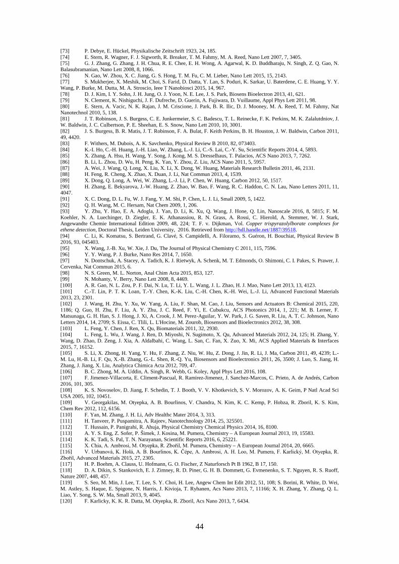
44
[73] P. Debye, E. Hückel, Physikalische Zeitschrift 1923, 24, 185. [74] E. Stern, R. Wagner, F. J. Sigworth, R. Breaker, T. M. Fahmy, M. A. Reed, Nano Lett 2007, 7, 3405. [75] G. J. Zhang, G. Zhang, J. H. Chua, R. E. Chee, E. H. Wong, A. Agarwal, K. D. Buddharaju, N. Singh, Z. Q. Gao, N. Balasubramanian, Nano Lett 2008, 8, 1066. [76] N. Gao, W. Zhou, X. C. Jiang, G. S. Hong, T. M. Fu, C. M. Lieber, Nano Lett 2015, 15, 2143. [77] S. Mukherjee, X. Meshik, M. Choi, S. Farid, D. Datta, Y. Lan, S. Poduri, K. Sarkar, U. Baterdene, C. E. Huang, Y. Y. Wang, P. Burke, M. Dutta, M. A. Stroscio, Ieee T Nanobiosci 2015, 14, 967. [78] D. J. Kim, I. Y. Sohn, J. H. Jung, O. J. Yoon, N. E. Lee, J. S. Park, Biosens Bioelectron 2013, 41, 621. [79] N. Clement, K. Nishiguchi, J. F. Dufreche, D. Guerin, A. Fujiwara, D. Vuillaume, Appl Phys Lett 2011, 98. [80] E. Stern, A. Vacic, N. K. Rajan, J. M. Criscione, J. Park, B. R. Ilic, D. J. Mooney, M. A. Reed, T. M. Fahmy, Nat Nanotechnol 2010, 5, 138. [81] J. T. Robinson, J. S. Burgess, C. E. Junkermeier, S. C. Badescu, T. L. Reinecke, F. K. Perkins, M. K. Zalalutdniov, J. W. Baldwin, J. C. Culbertson, P. E. Sheehan, E. S. Snow, Nano Lett 2010, 10, 3001. [82] J. S. Burgess, B. R. Matis, J. T. Robinson, F. A. Bulat, F. Keith Perkins, B. H. Houston, J. W. Baldwin, Carbon 2011, 49, 4420. [83] F. Withers, M. Dubois, A. K. Savchenko, Physical Review B 2010, 82, 073403. [84] K.-I. Ho, C.-H. Huang, J.-H. Liao, W. Zhang, L.-J. Li, C.-S. Lai, C.-Y. Su, Scientific Reports 2014, 4, 5893. [85] X. Zhang, A. Hsu, H. Wang, Y. Song, J. Kong, M. S. Dresselhaus, T. Palacios, ACS Nano 2013, 7, 7262. [86] B. Li, L. Zhou, D. Wu, H. Peng, K. Yan, Y. Zhou, Z. Liu, ACS Nano 2011, 5, 5957. [87] A. Wei, J. Wang, Q. Long, X. Liu, X. Li, X. Dong, W. Huang, Materials Research Bulletin 2011, 46, 2131. [88] H. Feng, R. Cheng, X. Zhao, X. Duan, J. Li, Nat Commun 2013, 4, 1539. [89] X. Dong, Q. Long, A. Wei, W. Zhang, L.-J. Li, P. Chen, W. Huang, Carbon 2012, 50, 1517. [90] H. Zhang, E. Bekyarova, J.-W. Huang, Z. Zhao, W. Bao, F. Wang, R. C. Haddon, C. N. Lau, Nano Letters 2011, 11, 4047. [91] X. C. Dong, D. L. Fu, W. J. Fang, Y. M. Shi, P. Chen, L. J. Li, Small 2009, 5, 1422. [92] Q. H. Wang, M. C. Hersam, Nat Chem 2009, 1, 206. [93] Y. Zhu, Y. Hao, E. A. Adogla, J. Yan, D. Li, K. Xu, Q. Wang, J. Hone, Q. Lin, Nanoscale 2016, 8, 5815; F. M. Koehler, N. A. Luechinger, D. Ziegler, E. K. Athanassiou, R. N. Grass, A. Rossi, C. Hierold, A. Stemmer, W. J. Stark, Angewandte Chemie International Edition 2009, 48, 224; T. F. v. Dijkman, Vol. Copper trispyrazolylborate complexes for ethene detection, Doctoral Thesis, Leiden University, 2016. Retrieved from http://hdl.handle.net/1887/39518. [94] C. Li, K. Komatsu, S. Bertrand, G. Clavé, S. Campidelli, A. Filoramo, S. Guéron, H. Bouchiat, Physical Review B 2016, 93, 045403. [95] X. Wang, J.-B. Xu, W. Xie, J. Du, The Journal of Physical Chemistry C 2011, 115, 7596. [96] Y. Y. Wang, P. J. Burke, Nano Res 2014, 7, 1650. [97] N. Dontschuk, A. Stacey, A. Tadich, K. J. Rietwyk, A. Schenk, M. T. Edmonds, O. Shimoni, C. I. Pakes, S. Prawer, J. Cervenka, Nat Commun 2015, 6. [98] N. S. Green, M. L. Norton, Anal Chim Acta 2015, 853, 127. [99] N. Mohanty, V. Berry, Nano Lett 2008, 8, 4469. [100] A. R. Gao, N. L. Zou, P. F. Dai, N. Lu, T. Li, Y. L. Wang, J. L. Zhao, H. J. Mao, Nano Lett 2013, 13, 4123. [101] C.-T. Lin, P. T. K. Loan, T.-Y. Chen, K.-K. Liu, C.-H. Chen, K.-H. Wei, L.-J. Li, Advanced Functional Materials 2013, 23, 2301. [102] J. Wang, H. Zhu, Y. Xu, W. Yang, A. Liu, F. Shan, M. Cao, J. Liu, Sensors and Actuators B: Chemical 2015, 220, 1186; Q. Guo, H. Zhu, F. Liu, A. Y. Zhu, J. C. Reed, F. Yi, E. Cubukcu, ACS Photonics 2014, 1, 221; M. B. Lerner, F. Matsunaga, G. H. Han, S. J. Hong, J. Xi, A. Crook, J. M. Perez-Aguilar, Y. W. Park, J. G. Saven, R. Liu, A. T. C. Johnson, Nano Letters 2014, 14, 2709; S. Eissa, C. Tlili, L. L'Hocine, M. Zourob, Biosensors and Bioelectronics 2012, 38, 308. [103] L. Feng, Y. Chen, J. Ren, X. Qu, Biomaterials 2011, 32, 2930. [104] L. Feng, L. Wu, J. Wang, J. Ren, D. Miyoshi, N. Sugimoto, X. Qu, Advanced Materials 2012, 24, 125; H. Zhang, Y. Wang, D. Zhao, D. Zeng, J. Xia, A. Aldalbahi, C. Wang, L. San, C. Fan, X. Zuo, X. Mi, ACS Applied Materials & Interfaces 2015, 7, 16152. [105] S. Li, X. Zhong, H. Yang, Y. Hu, F. Zhang, Z. Niu, W. Hu, Z. Dong, J. Jin, R. Li, J. Ma, Carbon 2011, 49, 4239; L.-M. Lu, H.-B. Li, F. Qu, X.-B. Zhang, G.-L. Shen, R.-Q. Yu, Biosensors and Bioelectronics 2011, 26, 3500; J. Luo, S. Jiang, H. Zhang, J. Jiang, X. Liu, Analytica Chimica Acta 2012, 709, 47. [106] B. C. Zhong, M. A. Uddin, A. Singh, R. Webb, G. Koley, Appl Phys Lett 2016, 108. [107] F. Jimenez-Villacorta, E. Climent-Pascual, R. Ramirez-Jimenez, J. Sanchez-Marcos, C. Prieto, A. de Andrés, Carbon 2016, 101, 305. [108] K. S. Novoselov, D. Jiang, F. Schedin, T. J. Booth, V. V. Khotkevich, S. V. Morozov, A. K. Geim, P Natl Acad Sci USA 2005, 102, 10451. [109] V. Georgakilas, M. Otyepka, A. B. Bourlinos, V. Chandra, N. Kim, K. C. Kemp, P. Hobza, R. Zboril, K. S. Kim, Chem Rev 2012, 112, 6156. [110] F. Yan, M. Zhang, J. H. Li, Adv Healthc Mater 2014, 3, 313. [111] H. Tanveer, P. Puspamitra, A. Rajeev, Nanotechnology 2014, 25, 325501. [112] T. Hussain, P. Panigrahi, R. Ahuja, Physical Chemistry Chemical Physics 2014, 16, 8100. [113] A. Y. S. Eng, Z. Sofer, P. Šimek, J. Kosina, M. Pumera, Chemistry – A European Journal 2013, 19, 15583. [114] K. K. Tadi, S. Pal, T. N. Narayanan, Scientific Reports 2016, 6, 25221. [115] X. Chia, A. Ambrosi, M. Otyepka, R. Zbořil, M. Pumera, Chemistry – A European Journal 2014, 20, 6665. [116] V. Urbanová, K. Holá, A. B. Bourlinos, K. Čépe, A. Ambrosi, A. H. Loo, M. Pumera, F. Karlický, M. Otyepka, R. Zbořil, Advanced Materials 2015, 27, 2305. [117] H. P. Boehm, A. Clauss, U. Hofmann, G. O. Fischer, Z Naturforsch Pt B 1962, B 17, 150. [118] D. A. Dikin, S. Stankovich, E. J. Zimney, R. D. Piner, G. H. B. Dommett, G. Evmenenko, S. T. Nguyen, R. S. Ruoff, Nature 2007, 448, 457. [119] S. Seo, M. Min, J. Lee, T. Lee, S. Y. Choi, H. Lee, Angew Chem Int Edit 2012, 51, 108; S. Borini, R. White, D. Wei, M. Astley, S. Haque, E. Spigone, N. Harris, J. Kivioja, T. Ryhanen, Acs Nano 2013, 7, 11166; X. H. Zhang, Y. Zhang, Q. L. Liao, Y. Song, S. W. Ma, Small 2013, 9, 4045. [120] F. Karlicky, K. K. R. Datta, M. Otyepka, R. Zboril, Acs Nano 2013, 7, 6434.
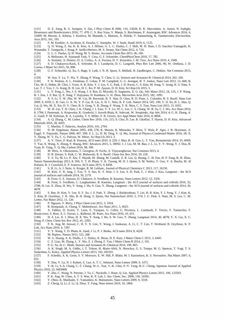
45
[121] D. E. Jiang, B. G. Sumpter, S. Dai, J Phys Chem B 2006, 110, 23628; R. K. Shervedani, A. Amini, N. Sadeghi, Biosensors and Bioelectronics 2016, 77, 478; C. S. Rao Vusa, V. Manju, S. Berchmans, P. Arumugam, RSC Advances 2016, 6, 33409; M. Mooste, E. Kibena, J. Kozlova, M. Marandi, L. Matisen, A. Niilisk, V. Sammelselg, K. Tammeveski, Electrochim. Acta 2015, 161, 195. [122] F. M. Koehler, A. Jacobsen, K. Ensslin, C. Stampfer, W. J. Stark, Small 2010, 6, 1125. [123] Q. H. Wang, Z. Jin, K. K. Kim, A. J. Hilmer, G. L. C. Paulus, C. J. Shih, M. H. Ham, J. D. Sanchez-Yamagishi, K. Watanabe, T. Taniguchi, J. Kong, P. Jarillo-Herrero, M. S. Strano, Nat Chem 2012, 4, 724. [124] G. L. C. Paulus, Q. H. Wang, M. S. Strano, Accounts Chem Res 2013, 46, 160. [125] A. Bellunato, H. Arjmandi Tash, Y. Cesa, G. F. Schneider, ChemPhysChem 2016, 17, 785. [126] A. Sinitskii, A. Dimiev, D. A. Corley, A. A. Fursina, D. V. Kosynkin, J. M. Tour, Acs Nano 2010, 4, 1949. [127] S. D. Chakarova-Kack, E. Schroder, B. I. Lundqvist, D. C. Langreth, Phys Rev Lett 2006, 96; W. Orellana, J. D. Correa, J Mater Sci 2015, 50, 898. [128] G. F. Schneider, Q. Xu, S. Hage, S. Luik, J. N. H. Spoor, S. Malladi, H. Zandbergen, C. Dekker, Nat Commun 2013, 4. [129] W. Sun, Y. Lu, Y. Wu, Y. Zhang, P. Wang, Y. Chen, G. Li, Sensors and Actuators B: Chemical 2014, 202, 160. [130] F. K. Perkins, A. L. Friedman, E. Cobas, P. M. Campbell, G. G. Jernigan, B. T. Jonker, Nano Lett 2013, 13, 668; B. Cho, M. G. Hahm, M. Choi, J. Yoon, A. R. Kim, Y. J. Lee, S. G. Park, J. D. Kwon, C. S. Kim, M. Song, Y. Jeong, K. S. Nam, S. Lee, T. J. Yoo, C. G. Kang, B. H. Lee, H. C. Ko, P. M. Ajayan, D. H. Kim, Sci Rep-Uk 2015, 5. [131] L. Y. Feng, L. Wu, J. S. Wang, J. S. Ren, D. Miyoshi, N. Sugimoto, X. G. Qu, Adv Mater 2012, 24, 125; J. P. Wang, B. J. Zou, J. Z. Rui, Q. X. Song, T. Kajiyama, H. Kambara, G. H. Zhou, Microchim Acta 2015, 182, 1095. [132] X. S. Li, Y. W. Zhu, W. W. Cai, M. Borysiak, B. Y. Han, D. Chen, R. D. Piner, L. Colombo, R. S. Ruoff, Nano Lett 2009, 9, 4359; L. B. Gao, G. X. Ni, Y. P. Liu, B. Liu, A. H. C. Neto, K. P. Loh, Nature 2014, 505, 190; Y. D. Su, H. L. Han, Q. Cai, Q. Wu, M. X. Xie, D. Y. Chen, B. S. Geng, Y. B. Zhang, F. Wang, Y. R. Shen, C. S. Tian, Nano Lett 2015, 15, 6501. [133] W. H. Lin, T. H. Chen, J. K. Chang, J. I. Taur, Y. Y. Lo, W. L. Lee, C. S. Chang, W. B. Su, C. I. Wu, Acs Nano 2014, 8, 1784; I. Pasternak, A. Krajewska, K. Grodecki, I. Jozwik-Biala, K. Sobczak, W. Strupinski, Aip Adv 2014, 4; G. H. Zhang, A. G. Guell, P. M. Kirkman, R. A. Lazenby, T. S. Miller, P. R. Unwin, Acs Appl Mater Inter 2016, 8, 8008. [134] A. Q. Zhang, C. M. Lieber, Chem Rev 2016, 116, 215; S. Choi, H. Lee, R. Ghaffari, T. Hyeon, D. H. Kim, Advanced Materials 2016, 28, 4203. [135] C. Mackin, T. Palacios, Analyst 2016, 141, 2704. [136] D. M. Engelman, Nature 2005, 438, 578; K. Murata, K. Mitsuoka, T. Hirai, T. Walz, P. Agre, J. B. Heymann, A. Engel, Y. Fujiyoshi, Nature 2000, 407, 599; Z. L. Li, H. M. Ding, Y. Q. Ma, Journal of Physics-Condensed Matter 2016, 28; X. Y. Zhang, W. Y. Fu, C. G. Palivan, W. Meier, Sci Rep-Uk 2013, 3. [137] A. V. Titov, P. Kral, R. Pearson, ACS nano 2010, 4, 229; J. Mao, R. H. Guo, L. T. Yan, Biomaterials 2014, 35, 6069; T. Yue, X. Wang, X. Zhang, F. Huang, RSC Advances 2015, 5, 30092; J. J. Liu, M. M. Bao, J. L. Li, Y. Y. Weng, Y. J. Dou, B. Yuan, K. Yang, Y. Q. Ma, Carbon 2016, 98, 300. [138] M. Hirtz, A. Oikonomou, T. Georgiou, H. Fuchs, A. Vijayaraghavan, Nat Commun 2013, 4. [139] D. R. Dreyer, S. Park, C. W. Bielawski, R. S. Ruoff, Chem Soc Rev 2010, 39, 228. [140] Y. S. Tu, M. Lv, P. Xiu, T. Huynh, M. Zhang, M. Castelli, Z. R. Liu, Q. Huang, C. H. Fan, H. P. Fang, R. H. Zhou, Nature Nanotechnology 2013, 8, 594; V. T. H. Pham, V. K. Truong, M. D. J. Quinn, S. M. Notley, Y. Guo, V. A. Baulin, M. Al Kobaisi, R. J. Crawford, E. P. Ivanova, ACS nano 2015, 9, 8458. [141] S. H. Li, A. J. Stein, A. Kruger, R. M. Leblanc, Journal of Physical Chemistry C 2013, 117, 16150. [142] H. Kim, Y. R. Jang, J. Yoo, Y. S. Seo, K. Y. Kim, J. S. Lee, S. D. Park, C. J. Kim, J. Koo, Langmuir : the ACS journal of surfaces and colloids 2014, 30, 2170. [143] R. Frost, G. E. Jonsson, D. Chakarov, S. Svedhem, B. Kasemo, Nano Letters 2012, 12, 3356. [144] R. Frost, S. Svedhem, C. Langhammer, B. Kasemo, Langmuir : the ACS journal of surfaces and colloids 2016, 32, 2708; H. Lei, X. Zhou, H. Wu, Y. Song, J. Hu, S. Guo, Y. Zhang, Langmuir : the ACS journal of surfaces and colloids 2014, 30, 4678. [145] S. Bae, H. Kim, Y. Lee, X. F. Xu, J. S. Park, Y. Zheng, J. Balakrishnan, T. Lei, H. R. Kim, Y. I. Song, Y. J. Kim, K. S. Kim, B. Ozyilmaz, J. H. Ahn, B. H. Hong, S. Iijima, Nat Nanotechnol 2010, 5, 574; J. U. Park, S. Nam, M. S. Lee, C. M. Lieber, Nat Mater 2012, 11, 120. [146] P. Nguyen, V. Berry, J Phys Chem Lett 2012, 3, 1024. [147] R. Kempaiah, A. Chung, V. Maheshwari, Acs Nano 2011, 5, 6025. [148] A. Fabbro, D. Scaini, V. Leon, E. Vazquez, G. Cellot, G. Privitera, L. Lombardi, F. Torrisi, F. Tomarchio, F. Bonaccorso, S. Bosi, A. C. Ferrari, L. Ballerini, M. Prato, Acs Nano 2016, 10, 615. [149] H. Z. Lei, X. J. Zhou, H. X. Wu, Y. Song, J. Hu, S. W. Guo, Y. Zhang, Langmuir 2014, 30, 4678; Y. X. Liu, X. C. Dong, P. Chen, Chem Soc Rev 2012, 41, 2283. [150] P. K. Ang, M. Jaiswal, C. H. Y. X. Lim, Y. Wang, J. Sankaran, A. Li, C. T. Lim, T. Wohland, B. Ozyilmaz, K. P. Loh, Acs Nano 2010, 4, 7387. [151] Y. Y. Wang, T. D. Pham, K. Zand, J. Li, P. J. Burke, ACS nano 2014, 8, 4228. [152] M. Peplow, Nature 2015, 522, 268. [153] W. G. Huang, A. K. Diallo, J. L. Dailey, K. Besar, H. E. Katz, J Mater Chem C 2015, 3, 6445. [154] C. Z. Liao, M. Zhang, L. Y. Niu, Z. J. Zheng, F. Yan, J Mater Chem B 2014, 2, 191. [155] P.-G. Su, H.-C. Shieh, Sensors and Actuators B: Chemical 2014, 190, 865. [156] A. K. Singh, M. A. Uddin, J. T. Tolson, H. Maire-Afeli, N. Sbrockey, G. S. Tompa, M. G. Spencer, T. Vogt, T. S. Sudarshan, G. Koley, Applied Physics Letters 2013, 102, 043101. [157] F. Schedin, A. K. Geim, S. V. Morozov, E. W. Hill, P. Blake, M. I. Katsnelson, K. S. Novoselov, Nat Mater 2007, 6, 652. [158] Y. Dan, Y. Lu, N. J. Kybert, Z. Luo, A. T. C. Johnson, Nano Letters 2009, 9, 1472. [159] Y.-R. Li, S.-h. Chang, C.-T. Chang, W.-L. Tsai, Y.-K. Chiu, P.-Y. Yang, H.-C. Cheng, Japanese Journal of Applied Physics 2016, 55, 04EM08. [160] Y. Zhu, C. Wang, N. Petrone, J. Yu, C. Nuckolls, J. Hone, Q. Lin, Applied Physics Letters 2015, 106, 123503. [161] P. K. Ang, W. Chen, A. T. S. Wee, K. P. Loh, J. Am. Chem. Soc. 2008, 130, 14392. [162] Y. Ohno, K. Maehashi, Y. Yamashiro, K. Matsumoto, Nano Letters 2009, 9, 3318. [163] Z. Cheng, Q. Li, Z. Li, Q. Zhou, Y. Fang, Nano letters 2010, 10, 1864.
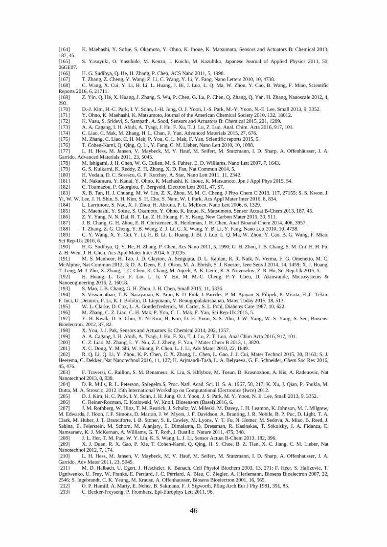
46
[164] K. Maehashi, Y. Sofue, S. Okamoto, Y. Ohno, K. Inoue, K. Matsumoto, Sensors and Actuators B: Chemical 2013, 187, 45. [165] S. Yasuyuki, O. Yasuhide, M. Kenzo, I. Koichi, M. Kazuhiko, Japanese Journal of Applied Physics 2011, 50, 06GE07. [166] H. G. Sudibya, Q. He, H. Zhang, P. Chen, ACS Nano 2011, 5, 1990. [167] T. Zhang, Z. Cheng, Y. Wang, Z. Li, C. Wang, Y. Li, Y. Fang, Nano Letters 2010, 10, 4738. [168] C. Wang, X. Cui, Y. Li, H. Li, L. Huang, J. Bi, J. Luo, L. Q. Ma, W. Zhou, Y. Cao, B. Wang, F. Miao, Scientific Reports 2016, 6, 21711. [169] Z. Yin, Q. He, X. Huang, J. Zhang, S. Wu, P. Chen, G. Lu, P. Chen, Q. Zhang, Q. Yan, H. Zhang, Nanoscale 2012, 4, 293. [170] D.-J. Kim, H.-C. Park, I. Y. Sohn, J.-H. Jung, O. J. Yoon, J.-S. Park, M.-Y. Yoon, N.-E. Lee, Small 2013, 9, 3352. [171] Y. Ohno, K. Maehashi, K. Matsumoto, Journal of the American Chemical Society 2010, 132, 18012. [172] K. Vasu, S. Sridevi, S. Sampath, A. Sood, Sensors and Actuators B: Chemical 2015, 221, 1209. [173] A. A. Cagang, I. H. Abidi, A. Tyagi, J. Hu, F. Xu, T. J. Lu, Z. Luo, Anal. Chim. Acta 2016, 917, 101. [174] C. Liao, C. Mak, M. Zhang, H. L. Chan, F. Yan, Advanced Materials 2015, 27, 676. [175] M. Zhang, C. Liao, C. H. Mak, P. You, C. L. Mak, F. Yan, Scientific reports 2015, 5. [176] T. Cohen-Karni, Q. Qing, Q. Li, Y. Fang, C. M. Lieber, Nano Lett 2010, 10, 1098. [177] L. H. Hess, M. Jansen, V. Maybeck, M. V. Hauf, M. Seifert, M. Stutzmann, I. D. Sharp, A. Offenhäusser, J. A. Garrido, Advanced Materials 2011, 23, 5045. [178] M. Ishigami, J. H. Chen, W. G. Cullen, M. S. Fuhrer, E. D. Williams, Nano Lett 2007, 7, 1643. [179] G. S. Kulkarni, K. Reddy, Z. H. Zhong, X. D. Fan, Nat Commun 2014, 5. [180] H. Vedala, D. C. Sorescu, G. P. Kotchey, A. Star, Nano Lett 2011, 11, 2342. [181] M. Nakamura, Y. Kanai, Y. Ohno, K. Maehashi, K. Inoue, K. Matsumoto, Jpn J Appl Phys 2015, 54. [182] C. Toumazou, P. Georgiou, P. Bergveld, Electron Lett 2011, 47, S7. [183] X. B. Tan, H. J. Chuang, M. W. Lin, Z. X. Zhou, M. M. C. Cheng, J Phys Chem C 2013, 117, 27155; S. S. Kwon, J. Yi, W. W. Lee, J. H. Shin, S. H. Kim, S. H. Cho, S. Nam, W. I. Park, Acs Appl Mater Inter 2016, 8, 834. [184] L. Larrimore, S. Nad, X. J. Zhou, H. Abruna, P. L. McEuen, Nano Lett 2006, 6, 1329. [185] K. Maehashi, Y. Sofue, S. Okamoto, Y. Ohno, K. Inoue, K. Matsumoto, Sensor Actuat B-Chem 2013, 187, 45. [186] Z. Y. Yang, N. N. Dai, R. T. Lu, Z. H. Huang, F. Y. Kang, New Carbon Mater 2015, 30, 511. [187] J. B. Chang, G. H. Zhou, E. R. Christensen, R. Heideman, J. H. Chen, Anal Bioanal Chem 2014, 406, 3957. [188] T. Zhang, Z. G. Cheng, Y. B. Wang, Z. J. Li, C. X. Wang, Y. B. Li, Y. Fang, Nano Lett 2010, 10, 4738. [189] C. Y. Wang, X. Y. Cui, Y. Li, H. B. Li, L. Huang, J. Bi, J. Luo, L. Q. Ma, W. Zhou, Y. Cao, B. G. Wang, F. Miao, Sci Rep-Uk 2016, 6. [190] H. G. Sudibya, Q. Y. He, H. Zhang, P. Chen, Acs Nano 2011, 5, 1990; G. H. Zhou, J. B. Chang, S. M. Cui, H. H. Pu, Z. H. Wen, J. H. Chen, Acs Appl Mater Inter 2014, 6, 19235. [191] M. S. Mannoor, H. Tao, J. D. Clayton, A. Sengupta, D. L. Kaplan, R. R. Naik, N. Verma, F. G. Omenetto, M. C. McAlpine, Nat Commun 2012, 3; D. A. Deen, E. J. Olson, M. A. Ebrish, S. J. Koester, Ieee Sens J 2014, 14, 1459; X. J. Huang, T. Leng, M. J. Zhu, X. Zhang, J. C. Chen, K. Chang, M. Aqeeli, A. K. Geim, K. S. Novoselov, Z. R. Hu, Sci Rep-Uk 2015, 5. [192] H. Huang, L. Tao, F. Liu, L. Ji, Y. Hu, M. M.-C. Cheng, P.-Y. Chen, D. Akinwande, Microsystems & Nanoengineering 2016, 2, 16018. [193] S. Mao, J. B. Chang, G. H. Zhou, J. H. Chen, Small 2015, 11, 5336. [194] S. Viswanathan, T. N. Narayanan, K. Aran, K. D. Fink, J. Paredes, P. M. Ajayan, S. Filipek, P. Miszta, H. C. Tekin, F. Inci, U. Demirci, P. Li, K. I. Bolotin, D. Liepmann, V. Renugopalakrishanan, Mater Today 2015, 18, 513. [195] W. L. Clarke, D. Cox, L. A. Gonderfrederick, W. Carter, S. L. Pohl, Diabetes Care 1987, 10, 622. [196] M. Zhang, C. Z. Liao, C. H. Mak, P. You, C. L. Mak, F. Yan, Sci Rep-Uk 2015, 5. [197] Y. H. Kwak, D. S. Choi, Y. N. Kim, H. Kim, D. H. Yoon, S.-S. Ahn, J.-W. Yang, W. S. Yang, S. Seo, Biosens. Bioelectron. 2012, 37, 82. [198] X. You, J. J. Pak, Sensors and Actuators B: Chemical 2014, 202, 1357. [199] A. A. Cagang, I. H. Abidi, A. Tyagi, J. Hu, F. Xu, T. J. Lu, Z. T. Luo, Anal Chim Acta 2016, 917, 101. [200] C. Z. Liao, M. Zhang, L. Y. Niu, Z. J. Zheng, F. Yan, J Mater Chem B 2013, 1, 3820. [201] X. C. Dong, Y. M. Shi, W. Huang, P. Chen, L. J. Li, Adv Mater 2010, 22, 1649. [202] R. Q. Li, Q. Li, Y. Zhou, K. P. Chen, C. X. Zhang, L. Chen, L. Gao, J. J. Cui, Mater Technol 2015, 30, B163; S. J. Heerema, C. Dekker, Nat Nanotechnol 2016, 11, 127; H. Arjmandi-Tash, L. A. Belyaeva, G. F. Schneider, Chem Soc Rev 2016, 45, 476. [203] F. Traversi, C. Raillon, S. M. Benameur, K. Liu, S. Khlybov, M. Tosun, D. Krasnozhon, A. Kis, A. Radenovic, Nat Nanotechnol 2013, 8, 939. [204] D. R. Mills, R. L. Peterson, Spiegelm.S, Proc. Natl. Acad. Sci. U. S. A. 1967, 58, 217; K. Xu, J. Qian, P. Shukla, M. Dutta, M. A. Stroscio, 2012 15th International Workshop on Computational Electronics (Iwce) 2012. [205] D. J. Kim, H. C. Park, I. Y. Sohn, J. H. Jung, O. J. Yoon, J. S. Park, M. Y. Yoon, N. E. Lee, Small 2013, 9, 3352. [206] C. Reiner-Rozman, C. Kotlowski, W. Knoll, Biosensors (Basel) 2016, 6. [207] J. M. Rothberg, W. Hinz, T. M. Rearick, J. Schultz, W. Mileski, M. Davey, J. H. Leamon, K. Johnson, M. J. Milgrew, M. Edwards, J. Hoon, J. F. Simons, D. Marran, J. W. Myers, J. F. Davidson, A. Branting, J. R. Nobile, B. P. Puc, D. Light, T. A. Clark, M. Huber, J. T. Branciforte, I. B. Stoner, S. E. Cawley, M. Lyons, Y. T. Fu, N. Homer, M. Sedova, X. Miao, B. Reed, J. Sabina, E. Feierstein, M. Schorn, M. Alanjary, E. Dimalanta, D. Dressman, R. Kasinskas, T. Sokolsky, J. A. Fidanza, E. Namsaraev, K. J. McKernan, A. Williams, G. T. Roth, J. Bustillo, Nature 2011, 475, 348. [208] J. L. Her, T. M. Pan, W. Y. Lin, K. S. Wang, L. J. Li, Sensor Actuat B-Chem 2013, 182, 396. [209] X. J. Duan, R. X. Gao, P. Xie, T. Cohen-Karni, Q. Qing, H. S. Choe, B. Z. Tian, X. C. Jiang, C. M. Lieber, Nat Nanotechnol 2012, 7, 174. [210] L. H. Hess, M. Jansen, V. Maybeck, M. V. Hauf, M. Seifert, M. Stutzmann, I. D. Sharp, A. Offenhausser, J. A. Garrido, Adv Mater 2011, 23, 5045. [211] M. D. Halbach, U. Egert, J. Hescheler, K. Banach, Cell Physiol Biochem 2003, 13, 271; F. Heer, S. Hafizovic, T. Ugniwenko, U. Frey, W. Franks, E. Perriard, J. C. Perriard, A. Blau, C. Ziegler, A. Hierlemann, Biosens Bioelectron 2007, 22, 2546; S. Ingebrandt, C. K. Yeung, M. Krause, A. Offenhausser, Biosens Bioelectron 2001, 16, 565. [212] O. P. Hamill, A. Marty, E. Neher, B. Sakmann, F. J. Sigworth, Pflug Arch Eur J Phy 1981, 391, 85. [213] C. Becker-Freyseng, P. Fromherz, Epl-Europhys Lett 2011, 96.
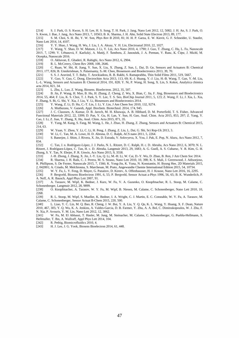
47
[214] S. J. Park, O. S. Kwon, S. H. Lee, H. S. Song, T. H. Park, J. Jang, Nano Lett 2012, 12, 5082; J. H. An, S. J. Park, O. S. Kwon, J. Bae, J. Jang, Acs Nano 2013, 7, 10563; B. K. Sharma, J. H. Ahn, Solid State Electron 2013, 89, 177. [215] S. M. Choi, S. H. Jhi, Y. W. Son, Phys Rev B 2010, 81; H. H. P. Garza, E. W. Kievit, G. F. Schneider, U. Staufer, Nano Lett 2014, 14, 4107. [216] Y. Y. Shao, J. Wang, H. Wu, J. Liu, I. A. Aksay, Y. H. Lin, Electroanal 2010, 22, 1027. [217] Y. Wang, Y. Shao, D. W. Matson, J. Li, Y. Lin, Acs Nano 2010, 4, 1790; J. Guo, T. Zhang, C. Hu, L. Fu, Nanoscale 2015, 7, 1290; V. Urbanová, F. Karlický, A. Matěj, F. Šembera, Z. Janoušek, J. A. Perman, V. Ranc, K. Čépe, J. Michl, M. Otyepka, Nanoscale 2016. [218] O. Akhavan, E. Ghaderi, R. Rahighi, Acs Nano 2012, 6, 2904. [219] R. L. McCreery, Chem Rev 2008, 108, 2646. [220] C. Ruan, W. Shi, H. Jiang, Y. Sun, X. Liu, X. Zhang, Z. Sun, L. Dai, D. Ge, Sensors and Actuators B: Chemical 2013, 177, 826; B. Unnikrishnan, S. Palanisamy, S.-M. Chen, Biosensors and Bioelectronics 2013, 39, 70. [221] S. S. J. Aravind, T. T. Baby, T. Arockiadoss, R. B. Rakhi, S. Ramaprabhu, Thin Solid Films 2011, 519, 5667. [222] Y. Guo, Y. Guo, C. Dong, Electrochim Acta 2013, 113, 69; K.-J. Huang, Y.-J. Liu, H.-B. Wang, T. Gan, Y.-M. Liu, L.-L. Wang, Sensors and Actuators B: Chemical 2014, 191, 828; Y. Ni, P. Wang, H. Song, X. Lin, S. Kokot, Analytica chimica acta 2014, 821, 34. [223] L. Zhu, L. Luo, Z. Wang, Biosens. Bioelectron. 2012, 35, 507. [224] B. Jin, P. Wang, H. Mao, B. Hu, H. Zhang, Z. Cheng, Z. Wu, X. Bian, C. Jia, F. Jing, Biosensors and Bioelectronics 2014, 55, 464; F. Liu, K. S. Choi, T. J. Park, S. Y. Lee, T. S. Seo, BioChip Journal 2011, 5, 123; Z. Wang, F. Li, J. Xia, L. Xia, F. Zhang, S. Bi, G. Shi, Y. Xia, J. Liu, Y. Li, Biosensors and Bioelectronics 2014. [225] Y. Wang, Z. Li, D. Hu, C.-T. Lin, J. Li, Y. Lin, J Am Chem Soc 2010, 132, 9274. [226] A. Muthurasu, V. Ganesh, Appl. Biochem. Biotechnol. 2014, 174, 945. [227] J. C. Claussen, A. Kumar, D. B. Jaroch, M. H. Khawaja, A. B. Hibbard, D. M. Porterfield, T. S. Fisher, Advanced Functional Materials 2012, 22, 3399; D. Pan, Y. Gu, H. Lan, Y. Sun, H. Gao, Anal. Chim. Acta 2015, 853, 297; Z. Yang, Y. Cao, J. Li, Z. Jian, Y. Zhang, X. Hu, Anal. Chim. Acta 2015, 871, 35. [228] Y. Yang, M. Kang, S. Fang, M. Wang, L. He, J. Zhao, H. Zhang, Z. Zhang, Sensors and Actuators B: Chemical 2015, 214, 63. [229] W. Yuan, Y. Zhou, Y. Li, C. Li, H. Peng, J. Zhang, Z. Liu, L. Dai, G. Shi, Sci Rep-Uk 2013, 3. [230] W. Li, C. Tan, M. A. Lowe, H. D. Abruna, D. C. Ralph, ACS nano 2011, 5, 2264. [231] S. Banerjee, J. Shim, J. Rivera, X. Jin, D. Estrada, V. Solovyeva, X. You, J. Pak, E. Pop, N. Aluru, Acs Nano 2012, 7, 834. [232] C. Tan, J. n. Rodríguez-López, J. J. Parks, N. L. Ritzert, D. C. Ralph, H. c. D. Abruña, Acs Nano 2012, 6, 3070; N. L. Ritzert, J. Rodríguez-López, C. Tan, H. c. D. Abruña, Langmuir 2013, 29, 1683; A. G. Guell, A. S. Cuharuc, Y. R. Kim, G. H. Zhang, S. Y. Tan, N. Ebejer, P. R. Unwin, Acs Nano 2015, 9, 3558. [233] J.-H. Zhong, J. Zhang, X. Jin, J.-Y. Liu, Q. Li, M.-H. Li, W. Cai, D.-Y. Wu, D. Zhan, B. Ren, J Am Chem Soc 2014. [234] R. Sharma, J. H. Baik, C. J. Perera, M. S. Strano, Nano Lett 2010, 10, 398; K. S. Mali, J. Greenwood, J. Adisoejoso, R. Phillipson, S. De Feyter, Nanoscale 2015, 7, 1566; K. Yong-Jin, K. Yuna, N. Konstantin, H. Byung Hee, 2D Materials 2015, 2, 042001; A. Criado, M. Melchionna, S. Marchesan, M. Prato, Angewandte Chemie International Edition 2015, 54, 10734. [235] W. Y. Fu, L. Y. Feng, D. Mayer, G. Panaitov, D. Kireev, A. Offenhausser, H. J. Krause, Nano Lett 2016, 16, 2295. [236] P. Bergveld, Biosens Bioelectron 1991, 6, 55; P. Bergveld, Sensor Actuat a-Phys 1996, 56, 65; B. K. Wunderlich, P. A. Neff, A. R. Bausch, Appl Phys Lett 2007, 91. [237] A. Tarasov, M. Wipf, K. Bedner, J. Kurz, W. Fu, V. A. Guzenko, O. Knopfmacher, R. L. Stoop, M. Calame, C. Schonenberger, Langmuir 2012, 28, 9899. [238] O. Knopfmacher, A. Tarasov, W. Y. Fu, M. Wipf, B. Niesen, M. Calame, C. Schonenberger, Nano Lett 2010, 10, 2268. [239] R. L. Stoop, M. Wipf, S. Mueller, K. Bedner, I. A. Wright, C. J. Martin, E. C. Constable, W. Y. Fu, A. Tarasov, M. Calame, C. Schonenberger, Sensor Actuat B-Chem 2015, 220, 500. [240] L. Liao, Y. C. Lin, M. Q. Bao, R. Cheng, J. W. Bai, Y. A. Liu, Y. Q. Qu, K. L. Wang, Y. Huang, X. F. Duan, Nature 2010, 467, 305; Y. Q. Wu, K. A. Jenkins, A. Valdes-Garcia, D. B. Farmer, Y. Zhu, A. A. Bol, C. Dimitrakopoulos, W. J. Zhu, F. N. Xia, P. Avouris, Y. M. Lin, Nano Lett 2012, 12, 3062. [241] W. Fu, M. El Abbassi, T. Hasler, M. Jung, M. Steinacher, M. Calame, C. Schonenberger, G. Puebla-Hellmann, S. Hellmuller, T. Ihn, A. Wallraff, Appl Phys Lett 2014, 104. [242] R. Pethig, Biomicrofluidics 2010, 4. [243] H. J. Lee, J. G. Yook, Biosens Bioelectron 2014, 61, 448.

![In situ fabrication of organic electrochemical transistors ... › upload › justPDF › 2462.pdf · potentials in building biosensors, such as sensing biochemical substances [2-4],](https://img.pdfslide.us/doc/110x75/5f1c86971ff39355e0489650/in-situ-fabrication-of-organic-electrochemical-transistors-a-upload-a-justpdf.jpg)


![Room-Temperature Humidity Sensing Using Graphene Oxide ...2 sensor based on hybrid films based on carbon nano-tubes and graphene [14]. Yoon et al. reported a CO 2 gas sensor using](https://img.pdfslide.us/doc/110x75/5e7bf3a08f70ea200d35b212/room-temperature-humidity-sensing-using-graphene-oxide-2-sensor-based-on-hybrid.jpg)