Embed Size (px)
DESCRIPTION
IEEE Journal Paper
Citation preview
336 IEEE TRANSACTIONS ON BIOMEDICAL CIRCUITS AND SYSTEMS, VOL. 6, NO. 4, AUGUST 2012
A Photovoltaic-Driven and Energy-AutonomousCMOS Implantable Sensor
Sahar Ayazian, Student Member, IEEE, Vahid A. Akhavan, Eric Soenen, Member, IEEE, andArjang Hassibi, Member, IEEE
Abstract—An energy-autonomous, photovoltaic (PV)-drivenand MRI-compatible CMOS implantable sensor is presented.On-chip -well diode arrays are used as CMOS-compatiblePV cells to harvest W’s of power from the light that penetratesinto the tissue. In this 2.5 mm 2.5 mm sub- W integratedsystem, the in-vivo physiological signals are first measured byusing a subthreshold ring oscillator-based sensor, the acquireddata is then modulated into a frequency-shift keying (FSK) signal,and finally transmitted neuromorphically to the skin surface byusing a pair of polarized electrodes.
Index Terms—CMOS, energy harvesting, implantable device,neuromorphic, photovoltaic cell, subthreshold.
I. INTRODUCTION
T ODAY, there is an ever-growing demand for compact, en-ergy autonomous, and noninvasive implantable biomed-
ical sensors. These devices, which continuously collect in-vivophysiological data, are imperative in the next generations of pa-tient monitoring systems. One of the fundamental challenges intheir implementation, besides the obvious size constraints andthe tissue-to-electronics biocompatibility impediments, is theefficient means to wirelessly deliver power to, and receive datafrom them.In the early generation of implantable devices, wires were
used to provide power and communicate the data from and tothe chip [1]. Although such an approach is still sparsely usedin neuroscience [2], it is not acceptable for patient monitoringapplications since it drastically increases the chance of infec-tion. In many applications today (e.g., pacemaker), batteries areimplanted with the device to provide long term power for theelectronics [3], [4]. This is despite the fact that batteries can bevery hazardous if they leak within the body [5]. Clearly, bat-teries have limited lifetimes and eventually will be fully dis-charged; yet it has been demonstrated that by implementing
Manuscript receivedMarch 27, 2011; revised June 26, 2011, August 29, 2011,and October 27, 2011; accepted November 04, 2011. Date of publication Jan-uary 23, 2012; date of current version July 24, 2012. This work was supportedby the Silicon Research Corporation (SRC). This paper was recommended byAssociate Editor T. Delbruck.S. Ayazian and A. Hassibi are with the Electrical and Computer Engineering
Department, The University of Texas at Austin, Austin, TX 78712 USA (e-mail:[email protected]; [email protected]).V. A. Akhavan is with the Chemical Engineering Department, The University
of Texas at Austin, Austin, TX 78712 USA (e-mail: [email protected]).E. Soenen is with the Taiwan Semiconductor Manufacturing Company,
Austin, TX 78759 USA (e-mail: [email protected]).Color versions of one or more of the figures in this paper are available online
at http://ieeexplore.ieee.org.Digital Object Identifier 10.1109/TBCAS.2011.2179030
Fig. 1. A photovoltaic-driven energy-autonomous CMOS implantable sensor.
ultra-low power embedded electronics, one can achieve yearsof functional operation in key applications [6].Recently, power delivery through inductive coupling (i.e.,
near-field coupling) has become popular [7]–[9]. Using thisapproach, one can directly power up the device or recharge theimplanted battery, if any. In this approach, efficient couplingfor reasonable power delivery necessitates proper alignmentbetween the external transmitter coils and the in-vivo receivercoils. An alternative approach along the same lines is to takeadvantage of far-field coupling of two antennae in RF frequen-cies and send power from transmitter to the receiver [10]. Inthis particular approach the direction of the radiated RF powerin view of the directivity of the in-vivo receiving antenna iscritical. In both of these methods, tissue introduces some loss inthe power delivery systems. This loss is generally larger in RFfrequency using antennas compared to the inductive couplingapproach [11], [12]. Regardless of the frequency used, thepresence of a relatively large coil or antenna is inevitable inboth methods. It is widely known that the larger they are (upto the order of the wavelength which is very large comparableto the size of the chip), the higher the delivered power can
1932-4545/$31.00 © 2012 IEEE
AYAZIAN et al.: A PHOTOVOLTAIC-DRIVEN AND ENERGY-AUTONOMOUS CMOS IMPLANTABLE SENSOR 337
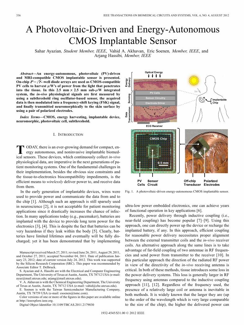
Fig. 2. Photodiodes available in bulk CMOS processes.
be. This is a fundamental disadvantage of this type of powerdelivery which also makes the implanted devices unsafe inMRI machines, i.e., MRI-incompatible.In this paper, an energy-autonomous and fully-integrated
CMOS implantable sensor chip is presented. The general ideais to take advantage of the existing on-chip photodiodes ofthe process as photovoltaic (PV) energy-harvesting photo-cells to power up the embedded circuitry (see Fig. 1). This2.5 mm 2.5 mm CMOS chip is capable of harvesting W’sof power from the ambient light passing through the tissueto perform real-time sensing while transmitting the acquireddata in a neuromorphic fashion and by using a set of in-vivopolarized electrodes [13]. The transmitted signal is picked upby a set of commercially available ECG electrodes. This powerharvesting system is MRI compatible since it requires no RFcoil or antenna and contains no paramagnetic material [14].An on-chip solar power harvesting circuit has been reported
in [15]. In this approach, the power harvesting block exists in aseparate die from the sensor.In Section II of this paper, the design, fabrication and charac-
terization of the CMOS integrated PV cells is described. More-over, the measured optical absorption of various types of tissueis reported to empirically demonstrate the feasibility of the pro-posed system and the fact that sufficient optical power can reachthe implanted CMOS chip. Next, in Section III, the architectureand circuit implementation of the sensor is described in detail,followed by the measurement results in Section IV. The conclu-sion comes last in Section V.
II. CMOS INTEGRATED PHOTOVOLTAIC (PV) CELL
In standard bulk CMOS processes, there are three types of PNjunctions (diodes) that can potentially operate as PV cells. Asshown in Fig. 2, these devices are ,and photodiodes. Since of bulk CMOS pro-cesses is always connected to the lowest possible voltage (V ),neither nor can be used as an on-chipPV cell. The reason being that in PV mode (i.e., forward bias),the anode of the diode ( for these two devices) becomesthe positive node of the PV cell, a condition which is not al-lowed in bulk CMOS processes. Hence, the only viable devicefor creating PV cells remains photodiode.In Fig. 3, the structure of the unit PV cell
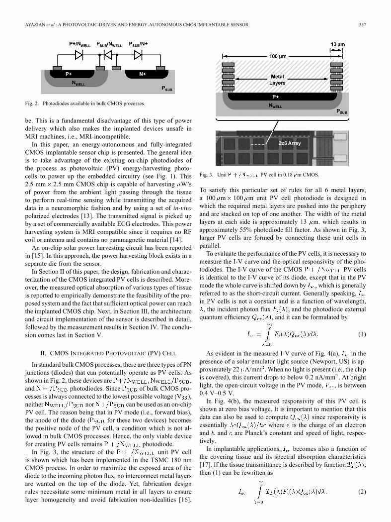
is shown which has been implemented in the TSMC 180 nmCMOS process. In order to maximize the exposed area of thediode to the incoming photon flux, no interconnect metal layersare wanted on the top of the diode. Yet, fabrication designrules necessitate some minimum metal in all layers to ensurelayer homogeneity and avoid fabrication non-idealities [16].
Fig. 3. Unit PV cell in 0.18 m CMOS.
To satisfy this particular set of rules for all 6 metal layers,a 100 m 100 m unit PV cell photodiode is designed inwhich the required metal layers are pushed into the peripheryand are stacked on top of one another. The width of the metallayers at each side is approximately 13 m. which results inapproximately 55% photodiode fill factor. As shown in Fig. 3,larger PV cells are formed by connecting these unit cells inparallel.To evaluate the performance of the PV cells, it is necessary to
measure the I-V curve and the optical responsivity of the pho-todiodes. The I-V curve of the CMOS PV cellsis identical to the I-V curve of its diode, except that in the PVmode the whole curve is shifted down by , which is generallyreferred to as the short-circuit current. Generally speaking,in PV cells is not a constant and is a function of wavelength,, the incident photon flux , and the photodiode externalquantum efficiency , and it can be formulated by
(1)
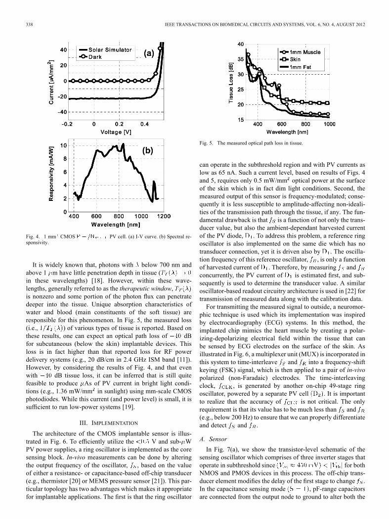
As evident in the measured I-V curve of Fig. 4(a), in thepresence of a solar emulator light source (Newport, US) is ap-proximately 22 A/mm .When no light is present (i.e., the chipis covered), this current drops to below 0.2 nA/mm . At brightlight, the open-circuit voltage in the PV mode, , is between0.4 V–0.5 V.In Fig. 4(b), the measured responsivity of this PV cell is
shown at zero bias voltage. It is important to mention that thisdata can also be used to compute since responsivity isessentially where is the charge of an electronand and are Planck’s constant and speed of light, respec-tively.In implantable applications, becomes also a function of
the covering tissue and its spectral absorption characteristics[17]. If the tissue transmittance is described by function ,then (1) can be rewritten as
(2)
338 IEEE TRANSACTIONS ON BIOMEDICAL CIRCUITS AND SYSTEMS, VOL. 6, NO. 4, AUGUST 2012
Fig. 4. 1 mm CMOS PV cell. (a) I-V curve. (b) Spectral re-sponsivity.
It is widely known that, photons with below 700 nm andabove 1 m have little penetration depth in tissue (in these wavelengths) [18]. However, within these wave-lengths, generally referred to as the therapeutic window,is nonzero and some portion of the photon flux can penetratedeeper into the tissue. Unique absorption characteristics ofwater and blood (main constituents of the soft tissue) areresponsible for this phenomenon. In Fig. 5, the measured loss(i.e., ) of various types of tissue is reported. Based onthese results, one can expect an optical path loss of dBfor subcutaneous (below the skin) implantable devices. Thisloss is in fact higher than that reported loss for RF powerdelivery systems (e.g., 20 dB/cm in 2.4 GHz ISM band [11]).However, by considering the results of Fig. 4, and that evenwith dB tissue loss, it can be inferred that is still quitefeasible to produce As of PV current in bright light condi-tions (e.g., 1.36 mW/mm in sunlight) using mm-scale CMOSphotodiodes. While this current (and power level) is small, it issufficient to run low-power systems [19].
III. IMPLEMENTATION
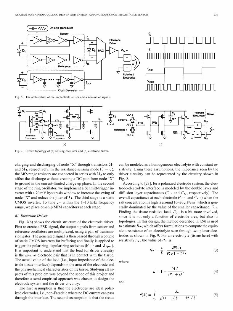
The architecture of the CMOS implantable sensor is illus-trated in Fig. 6. To efficiently utilize the V and sub- WPV power supplies, a ring oscillator is implemented as the coresensing block. In-vivo measurements can be done by alteringthe output frequency of the oscillator, , based on the valueof either a resistance- or capacitance-based off-chip transducer(e.g., thermistor [20] or MEMS pressure sensor [21]). This par-ticular topology has two advantages which makes it appropriatefor implantable applications. The first is that the ring oscillator
Fig. 5. The measured optical path loss in tissue.
can operate in the subthreshold region and with PV currents aslow as 65 nA. Such a current level, based on results of Figs. 4and 5, requires only 0.5 mW/mm optical power at the surfaceof the skin which is in fact dim light conditions. Second, themeasured output of this sensor is frequency-modulated; conse-quently it is less susceptible to amplitude-affecting non-ideali-ties of the transmission path through the tissue, if any. The fun-damental drawback is that is a function of not only the trans-ducer value, but also the ambient-dependant harvested currentof the PV diode, . To address this problem, a reference ringoscillator is also implemented on the same die which has notransducer connection, yet it is driven also by . The oscilla-tion frequency of this reference oscillator, , is only a functionof harvested current of . Therefore, by measuring andconcurrently, the PV current of is estimated first, and sub-sequently is used to determine the transducer value. A similaroscillator-based readout circuitry architecture is used in [22] fortransmission of measured data along with the calibration data.For transmitting the measured signal to outside, a neuromor-
phic technique is used which its implementation was inspiredby electrocardiography (ECG) systems. In this method, theimplanted chip mimics the heart muscle by creating a polar-izing-depolarizing electrical field within the tissue that canbe sensed by ECG electrodes on the surface of the skin. Asillustrated in Fig. 6, a multiplexer unit (MUX) is incorporated inthis system to time-interleave and into a frequency-shiftkeying (FSK) signal, which is then applied to a pair of in-vivopolarized (non-Faradaic) electrodes. The time-interleavingclock, , is generated by another on-chip 49-stage ringoscillator, powered by a separate PV cell . It is importantto realize that the accuracy of is not critical. The onlyrequirement is that its value has to be much less than and(e.g., below 200 Hz) to ensure that we can properly differentiateand detect and .
A. Sensor
In Fig. 7(a), we show the transistor-level schematic of thesensing oscillator which comprises of three inverter stages thatoperate in subthreshold since for bothNMOS and PMOS devices in this process. The off-chip trans-ducer element modifies the delay of the first stage to change .In the capacitance sensing mode , pF-range capacitorsare connected from the output node to ground to alter both the
AYAZIAN et al.: A PHOTOVOLTAIC-DRIVEN AND ENERGY-AUTONOMOUS CMOS IMPLANTABLE SENSOR 339
Fig. 6. The architecture of the implantable sensor and a scheme of signals.
Fig. 7. Circuit topology of (a) sensing oscillator and (b) electrode driver.
charging and discharging of node “X” through transistorsand , respectively. In the resistance sensing mode ,the M -range resistors are connected in series with to onlyaffect the discharge without creating a DC path from node “X”to ground in the current-limited charge up phase. In the secondstage of the ring oscillator, we implement a Schmitt-trigger in-verter with a 70 mV hysteresis window to increase the swing ofnode “X” and reduce the jitter of . The third stage is a staticCMOS inverter. To tune within the 1–10 kHz frequencyrange, we place on-chip MIM capacitors at each stage.
B. Electrode Driver
Fig. 7(b) shows the circuit structure of the electrode driver.First to create a FSK signal, the output signals from sensor andreference oscillators are multiplexed, using a pair of transmis-sion gates. The generated signal is then passed through a coupleof static CMOS inverters for buffering and finally is applied totrigger the polarizing-depolarizing switches ( and ).It is important to understand that the load for driver circuitryis the in-vivo electrode pair that is in contact with the tissue.The actual value of the load (i.e., input impedance of the elec-trode-tissue interface) depends on the area of the electrode andthe physiochemical characteristics of the tissue. Studying all as-pects of this problem was beyond the scope of this project andtherefore a semi-empirical approach was chosen to design theelectrode system and the driver circuitry.The first assumption is that the electrodes are ideal polar-
ized electrodes, i.e., non-Faradaic where no DC current can passthrough the interface. The second assumption is that the tissue
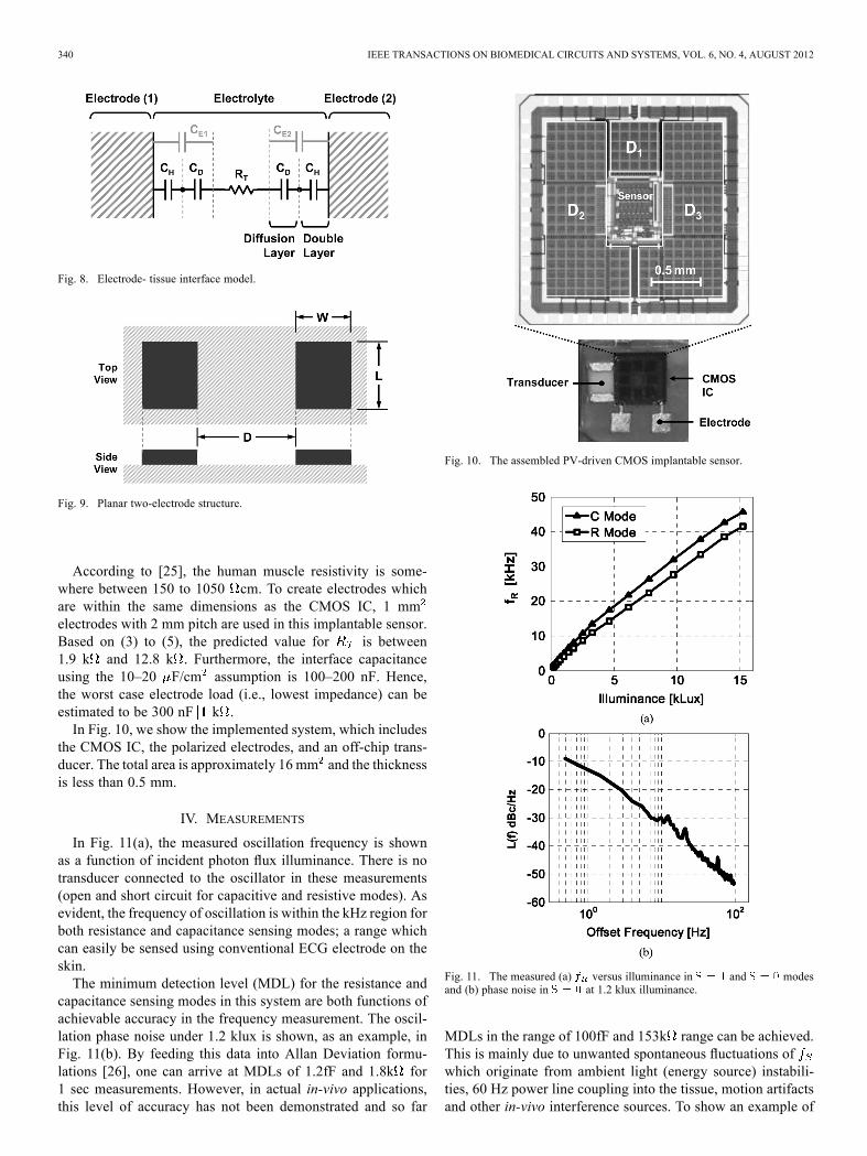
can be modeled as a homogeneous electrolyte with constant re-sistivity. Using these assumptions, the impedance seen by thedriver circuitry can be represented by the circuitry shown inFig. 8.According to [23], for a polarized electrode system, the elec-
trode-electrolyte interface is modeled by the double layer anddiffusion layer capacitances ( and , respectively). Theoverall capacitance at each electrode ( and ) when thesalt concentration is high is around 10–20 F/cm which is gen-erally dominated by the value of the smaller capacitance, .Finding the tissue resistive load, , is a bit more involved,since it is not only a function of electrode area, but also itstopologies. In this design, the method described in [24] is usedto estimate , which offers formulations to compute the equiv-alent resistance of an electrolyte seen through two planar elec-trodes as shown in Fig. 9. For an electrolyte (tissue here) withresistivity , the value of is
(3)
where
(4)
and
(5)
340 IEEE TRANSACTIONS ON BIOMEDICAL CIRCUITS AND SYSTEMS, VOL. 6, NO. 4, AUGUST 2012
Fig. 8. Electrode- tissue interface model.
Fig. 9. Planar two-electrode structure.
According to [25], the human muscle resistivity is some-where between 150 to 1050 cm. To create electrodes whichare within the same dimensions as the CMOS IC, 1 mmelectrodes with 2 mm pitch are used in this implantable sensor.Based on (3) to (5), the predicted value for is between1.9 k and 12.8 k . Furthermore, the interface capacitanceusing the 10–20 F/cm assumption is 100–200 nF. Hence,the worst case electrode load (i.e., lowest impedance) can beestimated to be 300 nF k .In Fig. 10, we show the implemented system, which includes
the CMOS IC, the polarized electrodes, and an off-chip trans-ducer. The total area is approximately 16 mm and the thicknessis less than 0.5 mm.
IV. MEASUREMENTS
In Fig. 11(a), the measured oscillation frequency is shownas a function of incident photon flux illuminance. There is notransducer connected to the oscillator in these measurements(open and short circuit for capacitive and resistive modes). Asevident, the frequency of oscillation is within the kHz region forboth resistance and capacitance sensing modes; a range whichcan easily be sensed using conventional ECG electrode on theskin.The minimum detection level (MDL) for the resistance and
capacitance sensing modes in this system are both functions ofachievable accuracy in the frequency measurement. The oscil-lation phase noise under 1.2 klux is shown, as an example, inFig. 11(b). By feeding this data into Allan Deviation formu-lations [26], one can arrive at MDLs of 1.2fF and 1.8k for1 sec measurements. However, in actual in-vivo applications,this level of accuracy has not been demonstrated and so far
Fig. 10. The assembled PV-driven CMOS implantable sensor.
Fig. 11. The measured (a) versus illuminance in and modesand (b) phase noise in at 1.2 klux illuminance.
MDLs in the range of 100fF and 153k range can be achieved.This is mainly due to unwanted spontaneous fluctuations ofwhich originate from ambient light (energy source) instabili-ties, 60 Hz power line coupling into the tissue, motion artifactsand other in-vivo interference sources. To show an example of
AYAZIAN et al.: A PHOTOVOLTAIC-DRIVEN AND ENERGY-AUTONOMOUS CMOS IMPLANTABLE SENSOR 341
Fig. 12. Output spectrum of the sensing oscillator with (a) conventional lightbulb and (b) DC LED light source.
Fig. 13. Sensor transfer function in (a) resistive and (b) capacitive modes.
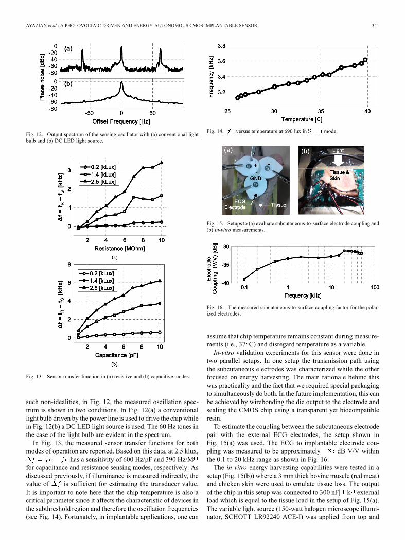
such non-idealities, in Fig. 12, the measured oscillation spec-trum is shown in two conditions. In Fig. 12(a) a conventionallight bulb driven by the power line is used to drive the chip whilein Fig. 12(b) a DC LED light source is used. The 60 Hz tones inthe case of the light bulb are evident in the spectrum.In Fig. 13, the measured sensor transfer functions for both
modes of operation are reported. Based on this data, at 2.5 klux,has a sensitivity of 600 Hz/pF and 390 Hz/M
for capacitance and resistance sensing modes, respectively. Asdiscussed previously, if illuminance is measured indirectly, thevalue of is sufficient for estimating the transducer value.It is important to note here that the chip temperature is also acritical parameter since it affects the characteristic of devices inthe subthreshold region and therefore the oscillation frequencies(see Fig. 14). Fortunately, in implantable applications, one can
Fig. 14. versus temperature at 690 lux in mode.
Fig. 15. Setups to (a) evaluate subcutaneous-to-surface electrode coupling and(b) in-vitro measurements.
Fig. 16. The measured subcutaneous-to-surface coupling factor for the polar-ized electrodes.
assume that chip temperature remains constant during measure-ments (i.e., 37 C) and disregard temperature as a variable.In-vitro validation experiments for this sensor were done in
two parallel setups. In one setup the transmission path usingthe subcutaneous electrodes was characterized while the otherfocused on energy harvesting. The main rationale behind thiswas practicality and the fact that we required special packagingto simultaneously do both. In the future implementation, this canbe achieved by wirebonding the die output to the electrode andsealing the CMOS chip using a transparent yet biocompatibleresin.To estimate the coupling between the subcutaneous electrode
pair with the external ECG electrodes, the setup shown inFig. 15(a) was used. The ECG to implantable electrode cou-pling was measured to be approximately dB V/V withinthe 0.1 to 20 kHz range as shown in Fig. 16.The in-vitro energy harvesting capabilities were tested in a
setup (Fig. 15(b)) where a 3 mm thick bovine muscle (red meat)and chicken skin were used to emulate tissue loss. The outputof the chip in this setup was connected to 300 nF k externalload which is equal to the tissue load in the setup of Fig. 15(a).The variable light source (150-watt halogen microscope illumi-nator, SCHOTT LR92240 ACE-I) was applied from top and

342 IEEE TRANSACTIONS ON BIOMEDICAL CIRCUITS AND SYSTEMS, VOL. 6, NO. 4, AUGUST 2012
Fig. 17. Measured FSK output with tissue for 15 klux.
normal to the skin surface, while the CMOS chip was placedunder the tissue. The illuminance in this setup was measured tobe 15 klux which is equivalent to the illuminance of a sunny daywith scattered clouds. Based on this number, 1.2 W is avail-able at the surface of the chip when no tissue is present. Thepresence of the tissue used in this setup attenuates this availablepower to approximately 120 nW.Since the sensor circuitry input impedance do not coincide
with the optimum operating point of the PV cells, the PV cellpower transfer efficiency (the ratio between consumed to themaximum available power) was estimated to be around 23%.In average, the sensor and reference blocks consumed around11 nW and the electrode driver consumes 19 nW.The measured output FSK signal is shown in Fig. 17. The fre-
quency difference between the reference and the sensor phasesin the FSK signal demonstrates the value of the measured ca-pacitor which was 10 pF. This particular result, considering themV-range amplitude at the output of the CMOS chip, demon-strates that we can produce 10–100 V FSK signals on the skin.This value is well within the detection range of ECG systems.
V. CONCLUSION
The results reported in this paper demonstrate the feasibilityof monolithically integrated CMOS PV-driven implantable sen-sors. The new architecture presented in the implemented CMOSchip also offers an alternative method for creating low-cost andmass-deployable energy autonomous ICs in biomedical appli-cations and beyond.While CMOS PV cells can directly power-up in-vivo sensors,
the delivered power is a function of the ambient light sourcesand the inherent uncertainty associated with them. To mitigatethis problem in future, it is appropriate to add energy storageelements (batteries or super capacitors) to the system and usethe PV cells as only the energy harvester. The implant in thatcase will still be energy autonomous and can also function whenthere is no ambient light present at the surface of the skin.
ACKNOWLEDGMENT
The authors would like to thank B. Fallahazad for his in-sightful suggestions, Taiwan Semiconductor ManufacturingCompany (TSMC) for foundry support, and TBioCAS anony-mous reviewers for their volunteer efforts to improve thissubmitted paper.
REFERENCES[1] J. Ji and K. D. Wise, “An implantable CMOS circuit interface for mul-
tiplexed multielectrode recording arrays,” IEEE J. Solid-State Circuits,vol. 27, pp. 433–443, Mar. 1992.
[2] G. Santhanam, M. D. Linderman, V. Gilja, A. Afshar, S. I. Ryu, T. H.Meng, and K. V. Shenoy, “HermesB: A continuous neural recordingsystem for freely behaving primates,” IEEE Trans. Biomed. Eng., vol.54, no. 11, pp. 2037–2050, Nov. 2007.
[3] A. M. Leung, W. H. Ko, T. M. Spear, and J. A. Bettice, “Intracranialpressure telemetry system using semicustom integrated circuits,” IEEETrans. Biomed. Eng., vol. BME-33, pp. 386–395, Apr. 1986.
[4] M. G. Dorman, M. A. Prisbe, and J. D. Meindl, “A monolithic signalprocessor for a neurophysiological telemetry system,” IEEE. J. Solid-State Circuits, vol. SC-20, pp. 1185–1193, Dec. 1985.
[5] T. Akin, K. Najafi, and R. M. Bradley, “A wireless implantable mul-tichannel digital neural recording system for a micromachined sieveelectrode,” IEEE J. Solid-State Circuits, vol. 33, no. 1, pp. 109–118,Jan. 1998.
[6] P. M. Zoll, H. A. Frank, L. R. N. Zarsky, A. J. Linenthal, and A. H.Belgard, “Long-term electric stimulation of the heart for Stokes-Adamsdisease,” Ann. Surg., vol. 154, p. 330, 196l.
[7] B. Smith, P. H. Peckham, M. W. Keith, and D. D. Roscoe, “An exter-nally powered, multichannel, implantable stimulator for versatile con-trol of paralyzed muscle,” IEEE Trans. Biomed. Eng., vol. BME-34,pp. 499–508, Jul. 1987.
[8] H. V. Allen, J. W. Knutti, and J. D. Meindl, “Integrated power con-trollers and RF data transmitters for totally implantable telemetry,”Biotel. Patient Monit., vol. 6, pp. 147–159, 1979.
[9] D. C. Galbraith, “An implantable multichannel neural stimulator,”Ph.D. dissertation, Stanford Univ., Stanford, CA, Dec. 1984.
[10] L. Yang, E. Y. Chow, P. P. Irazoqui, and W. Chappell, “RF pow-ering for embedded glaucoma sensors in miniature packages,” in Proc.Union Radio Scientifique Internationale General Assembly, Chicago,IL, Aug. 2008.
[11] D. Kurup, W. Joseph, G. Vermeeren, and L. Martens, “Path-loss modelfor in-body communication in homogeneous human muscle tissue,”Electron. Lett., vol. 45, no. 9, pp. 453–454, Apr. 2009.
[12] M. R. Yuce, S. W. P. Ng, N. L. Myo, J. Y. Khan, andW. Liu, “Wirelessbody sensor network using medical implant band,” J. Med. Syst., vol.31, no. 6.
[13] T. Handa et al., “A very low-power consumption wireless ECG mon-itoring system using body as a signal transmission medium,” in Proc.Solid-State Sensors, Actuators and Microsystems Conf., Chicago, IL,1997, vol. 2, pp. 1003–1006.
[14] U. Jow and M. Ghovanloo, “Optimization of data coils in a multibandwireless link for a neuroprosthetic implantable devices,” IEEE Trans.Biomed. Circuits Syst., vol. 4, no. 5, pp. 301–310, Jun. 2010.
[15] N. Guilar, A. Chen, T. Kleeburg, D. Yankelevich, and R. Amirtharajah,“Integrated solar energy harvesting and storage,” IEEE Trans. VeryLarge Scale Integr. (VLSI) Syst., vol. 17, no. 5, pp. 627–637,May 2009.
[16] A. Hastings, The Art of Analog Layout. Englewood Cliffs, NJ:Pearson Prentice Hall, 2006.
[17] W. F. Cheong et al., “A review of the optical properties of biologicaltissues,” IEEE J. Quantum Electron., vol. 26, no. 12, pp. 2166–2185,Dec. 1990.
[18] K. Konig, “Multiphoton microscopy in life sciences,” J. Microsc., vol.200, no. 2, pp. 83–104, Nov. 2000.
[19] G. Chen et al., “Millimeter-scale nearly perpetual sensor for systemstacked battery and solar cells,” in Proc. ISSCCDig. Tech. Papers, Feb.2010, pp. 288–289.
[20] D. Siegel, I. Garabieta, and J. Hollerbach, “An integrated tactile andthermal sensor,” in Proc. Int. Conf. Robotics and Automation, 1986,vol. 3, pp. 1286–1291.
[21] M. Ylimaula, M. Aberg, J. Kiihamaki, and H. Ronkainen, “Mono-lithic SOI-MEMS capacitive pressure sensor with standard bulk CMOSreadout circuit,” in Proc. 29th Euro. Solid-State Circuits Conf., Sep..2003, pp. 611–614.
[22] Y. Shih, T. Shen, and B. Otis, “A 2.3 uW intraocular pressure/temper-ature monitor,” in Proc. IEEE Asian Solid-State Circuits Conf., Nov.2010.
[23] A. Hassibi, R. Navid, R. W. Dutton, and T. H. Lee, “Comprehensivestudy of noise processes in electrode electrolyte interfaces,” J. Appl.Phys., vol. 96, no. 2, pp. 1074–1082, Jul. 2004.
[24] P. Jacobs, A. Varlan, and W. Sansen, “Design optimisation of planarelectrolytic conductivity sensors,” Med. Biol. Eng. Comput., vol. 33,pp. 802–810, Nov. 1995.
[25] T. J. C. Faes, H. A. van der Meij, J. C. De Munk, and R. M. Heethar,“The electric resistivity of human tissues (100 Hz–10 MHz): A meta-analysis of review studies,” Phys. Meas., vol. 20, no. 4, pp. R1–R10,1999.
[26] P. C. Chang, H. M. Peng, and S. Y. Lin, “Allan variance estimatedby phase noise measurements,” in Proc. 36th Annu. Precise Time andTime Interval Meeting, 2004.
AYAZIAN et al.: A PHOTOVOLTAIC-DRIVEN AND ENERGY-AUTONOMOUS CMOS IMPLANTABLE SENSOR 343
Sahar Ayazian (S’98) received the B.S. degree fromthe University of Tehran, Tehran, Iran, and the M.S.degree from the Sharif University of Technology,Tehran, Iran, both in electrical engineering, in 2001and 2003, respectively.She is working toward the Ph.D. degree in the
Electrical and Computer Engineering Department,The University of Texas at Austin. Her currentresearch project focuses on photovoltaic-basedimplants and challenges related to in-vivo integratedbiosensors.
Vahid A. Akhavan received the B.S. degree inchemical engineering from The University of Texasat Austin in 2006.He is working toward the Ph.D. degree at The Uni-
versity of Texas at Austin, where he is an EngineeringGraduate Research Aassistant. His research focuseson production of photovoltaic devices from colloidalnanoparticles and investigating electrical propertiesof nanocrystalline films.
Eric Soenen (M’87) received the B.S. degree fromthe Katholieke Universiteit Leuven, Leuven, Bel-gium, the M.S. and Ph.D. degrees from Texas A&MUniversity, College Station, and the MBA degreefrom the University of Texas at Austin.In 1991, he joined Texas Instruments Incorporated,
Dallas, TX, and led the data converter design effortsfrom 1995. In 2002, he joined Barcelona Design, aSilicon Valley startup. He rejoined Texas InstrumentsIncorporated in 2004 as part of the Wireless Termi-nals Business Unit. In 2007, he opened Taiwan Semi-
conductor Manufacturing Company’s Austin Design Center, focusing on R&Din the area of power management and analog circuits. He was elected TSMCAcademician in 2008. He has authored or coauthored over 25 U.S. patents.
Arjang Hassibi (S’99–M’05) received the B.Sc.degree (Hons.) in electrical engineering from theUniversity of Tehran, Tehran, Iran, in 1997, and theM.S. and Ph.D. degrees in electrical engineeringfrom Stanford University, Stanford, CA, in 2001 and2005, respectively.From 2005 to 2006, he was a Postdoctoral Scholar
in the Department of Electrical Engineering, Cali-fornia Institute of Technology, Pasadena. Since 2006,he has been with the Department of Electrical andComputer Engineering, The University of Texas at
Austin, where he is an Assistant Professor. He has also held research positionsat IBM T.J. Watson Reserach Center, Barcelona Design, Stanford GenomeTechnology Center, and Xagros Genomics, which he cofounded in 2001. Hisareas of interest are complementary metal-oxide semiconductor biochips,analog and mixed-signal circuit design, biotechnology, and spectroscopy.