Embed Size (px)
Citation preview
1
Bio-inspired Electronics for Interfacing Artificial Implants to Living Systems
Abstract
Imagine a world in which damaged parts of the body - an arm, an eye, or even a region of the brain – can be replaced by artificial implants capable of restoring or even enhancing human performance. The associated improvements in the quality of life would revolutionize the medical world and produce sweeping changes across society. This imagined world can be brought into reality by optimizing the fundamental science at the interface between the artificial and biological systems. In this science/engineering research proposal, we will simulate, fabricate and test a novel electronic-nerve interface. Our bio-inspired ‘interconnects’ will have the same geometry as the nerves they interface with. This will radically improve electrical stimulation of nerves in the human retina, the brain, the limbs and other parts of the body. In particular, they will allow victims of retinal diseases to see in greater detail and under more realistic lighting conditions compared to retinal implants using conventional interconnects. Implants using our interconnects will also be capable of color vision. The ultimate aim is to restore vision to the point that recipients can read text and facial expressions – crucial capabilities for functioning in society. Our generic interconnects could also address other neurological disorders, such as Parkinson’s disease and depression, and improve nerve connections to prosthetic limbs.
2
Executive Summary 1. Methodology/Implementation Our bodies are ‘wired’ using neurons: they connect the retina’s photoreceptors to the brain, allowing us to see; they also connect regions of the brain, allowing us to think. Yet today’s human implants are not optimally designed to interact with them. Implants are based on the simple metallic wires found in commercial electronics. Neurons belong to a distinctly different geometry. Neurons are fractal, featuring dendritic branches that repeat at increasingly fine sizes. This mismatch in basic geometry leads to low performance. For example, in eye implants less than 10 per cent of its interconnects are believed to successfully stimulate retinal neurons [1]. Serving as a generic implant-neuron interface, we propose metallic interconnects consisting of fractal branch patterns that match the neuron dendrites. This novel idea of ‘biophilic’ interconnects won an Innocentive Prize in 2014 (partially funded by the WMKF), beating 950 competing ideas and leading to 2 visits to the White House. Based on our preliminary research, the aim is for each neuron dendrite to automatically seek out and adhere to an interconnect branch. Consequently, when we apply a voltage to the interconnects to induce signals in the neurons, this ‘one-to-one’ adhesion will generate unprecedented stimulation. We also aim for ‘selective’ adhesion, whereby targeted types of neuron will adhere to specific interconnects. This novel capability will revolutionize applications of human implants. Considering the eye as our primary example, the retina features 4 types of neuron. These perform different functions when passing signals from the photoreceptors to the brain. Successful implants will need to select which neuron types to stimulate. We aim to achieve selective adhesion (and consequently selective stimulation) by matching the specific fractal properties of the interconnects to those of the target neurons. In addition to stimulating the neurons, the interconnects serve a second vital function – they control the light entering the implant’s photodiodes (which then convert the light into the stimulating voltage). We aim to optimize the interconnects’ optical properties so that the fractal branches filter the different light colors based on their wavelengths. This will allow the implant’s photodiodes to selectively receive red, green, and blue light. This ‘RGB’ sensitivity will mimic the RGB photoreceptors in the eye allowing the first color vision implants.
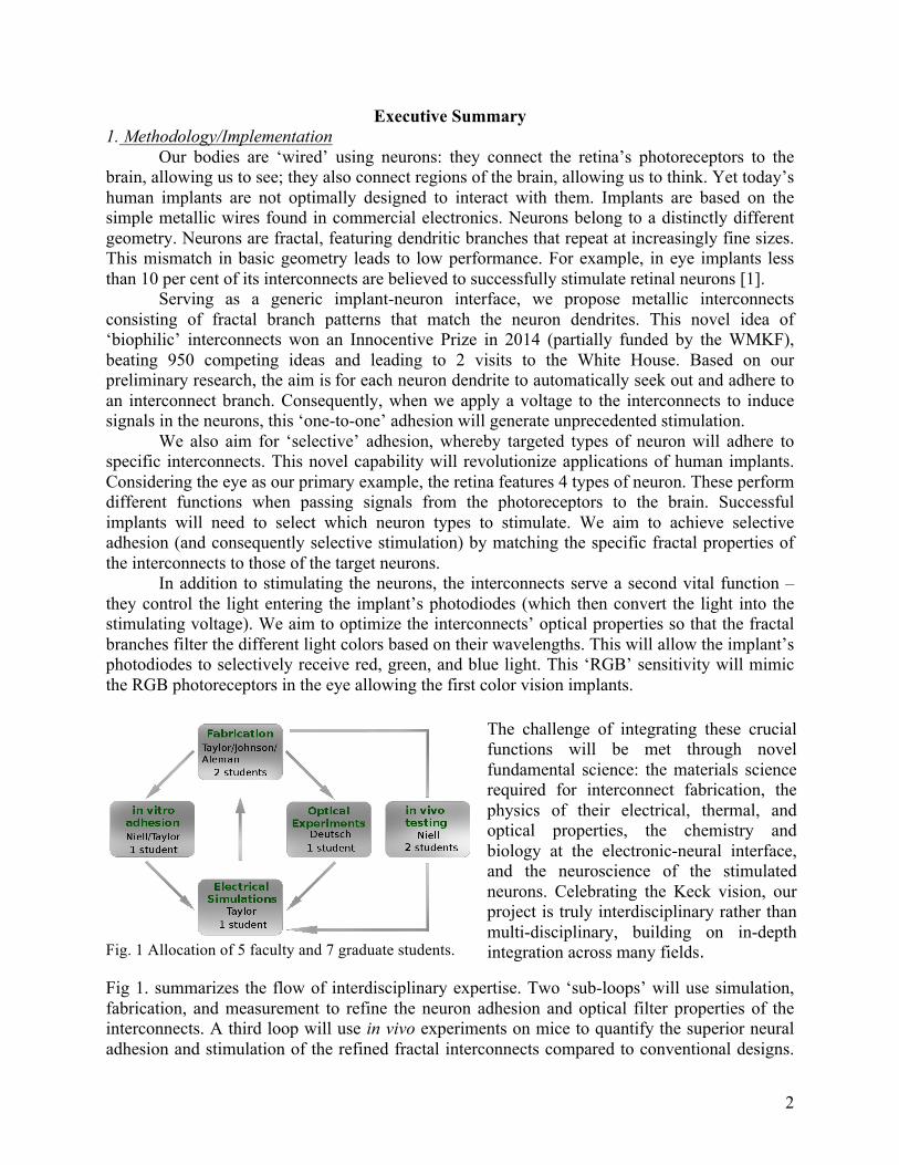
Fig. 1 Allocation of 5 faculty and 7 graduate students. Fig 1. summarizes the flow of interdisciplinary expertise. Two ‘sub-loops’ will use simulation, fabrication, and measurement to refine the neuron adhesion and optical filter properties of the interconnects. A third loop will use in vivo experiments on mice to quantify the superior neural adhesion and stimulation of the refined fractal interconnects compared to conventional designs.
The challenge of integrating these crucial functions will be met through novel fundamental science: the materials science required for interconnect fabrication, the physics of their electrical, thermal, and optical properties, the chemistry and biology at the electronic-neural interface, and the neuroscience of the stimulated neurons. Celebrating the Keck vision, our project is truly interdisciplinary rather than multi-disciplinary, building on in-depth integration across many fields.

3
All loops will operate concurrently over the 3 years with a gradual shift in emphasis from the in vitro to in vivo experiments. In addition to 2 visits by our Lund collaborators, the University of Oregon (UO) will host a workshop inviting external experts to discuss our results in year 2. 2. Personnel The major challenge of this project lies in assembling the optimal team of researchers. The proposal developed from Materials Science Institute Director Richard Taylor’s 30 years experience in the fabrication, computer simulation, and measurement of nanoelectronic devices. He is also a leading expert in fractal analysis and has 15 years of collaboration with cognitive neuroscientists. Taylor will co-ordinate the overall project, and play a primary role in 1) the fabrication of interconnects based on statistical fractal geometries, 2) in vitro adhesion experiments, and 3) simulation of the interconnects’ electrical properties. Chemistry Professor Darren Johnson is co-PI of the National Science Foundation (NSF) Center for Sustainable Materials Chemistry and an expert in organic and inorganic chemistry. He will 1) lead the fabrication of interconnects based on exact fractal geometries, and 2) functionalize the interconnect surfaces using organic chemistry treatment. Physics Assistant Professor Benjamin Alemán’s speciality focuses on the materials science, device fabrication, and the electrical measurements of carbon nanotubes. He will develop fractal networks of carbon nanotubes for constructing three-dimensional interconnects. Physics Professor Miriam Deutsch is a leading researcher in the fabrication, measurement, and modelling of the optical effects of patterned metallic systems, including fractal geometries. She will measure and model the optical filtering behaviour and associated thermal properties of the interconnects. Biology Assistant Professor Cristopher Niell will perform in vivo experiments in mice to determine the stimulation and adhesion efficacy of our implants. With a background in cognitive neuroscience, Niell is an expert in experimental techniques and data analysis of the mouse visual system. This team will continue a collaboration with key personnel at Lund University (Sweden): Neuroscientist and Ophthalmologist Maria Thereza Perez, Nanobiophysics and Solid-state Physicist Christelle Prinz (both experts in in vitro neuron experiments) and Nanophysics Professor and Director of the Nanometer Structure Consortium, Heiner Linke. Perez will collaborate on the adhesion experiments at the UO. Prinz and Linke will advise on fabrication methods, including constructing fractal interconnects on flexible substrates.
4
Project Narrative 1. Elaboration of Objectives/Aims/Impact
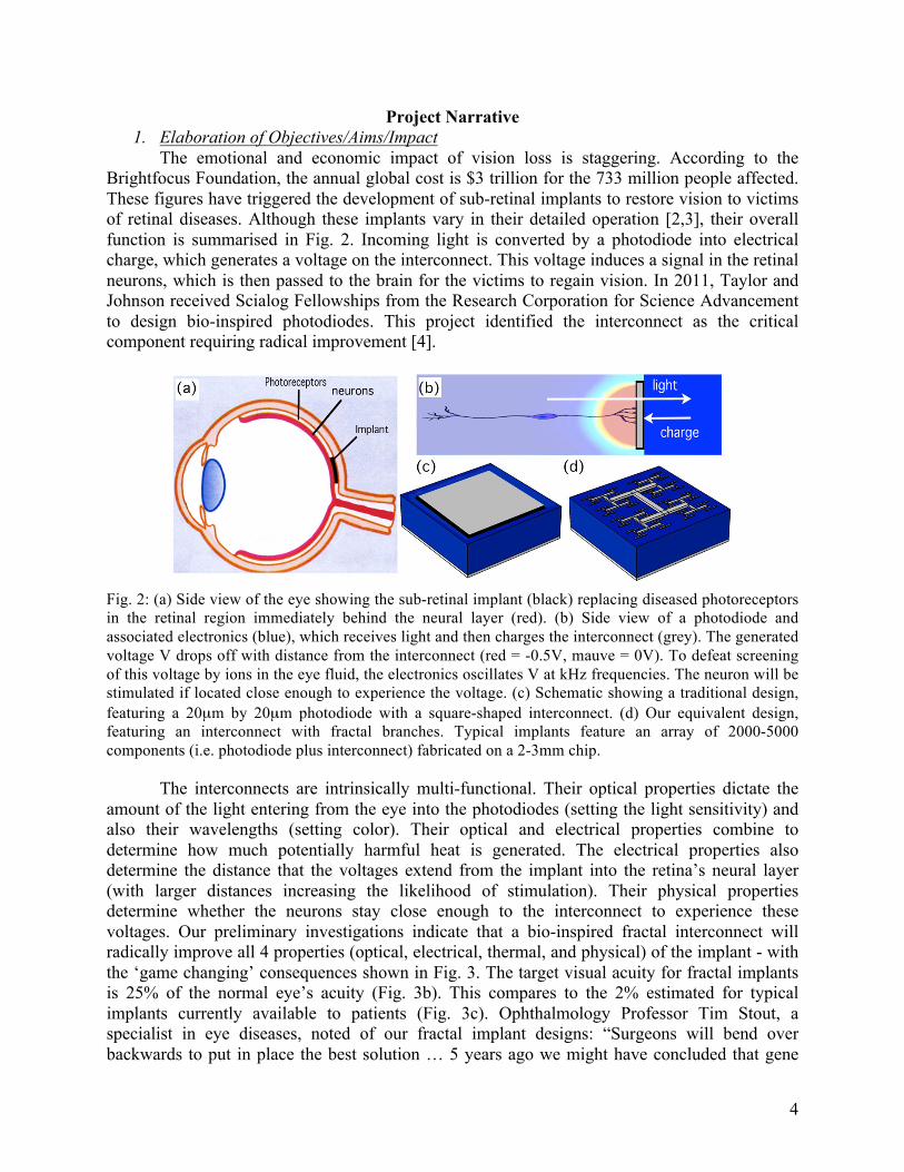
The emotional and economic impact of vision loss is staggering. According to the Brightfocus Foundation, the annual global cost is $3 trillion for the 733 million people affected. These figures have triggered the development of sub-retinal implants to restore vision to victims of retinal diseases. Although these implants vary in their detailed operation [2,3], their overall function is summarised in Fig. 2. Incoming light is converted by a photodiode into electrical charge, which generates a voltage on the interconnect. This voltage induces a signal in the retinal neurons, which is then passed to the brain for the victims to regain vision. In 2011, Taylor and Johnson received Scialog Fellowships from the Research Corporation for Science Advancement to design bio-inspired photodiodes. This project identified the interconnect as the critical component requiring radical improvement [4].
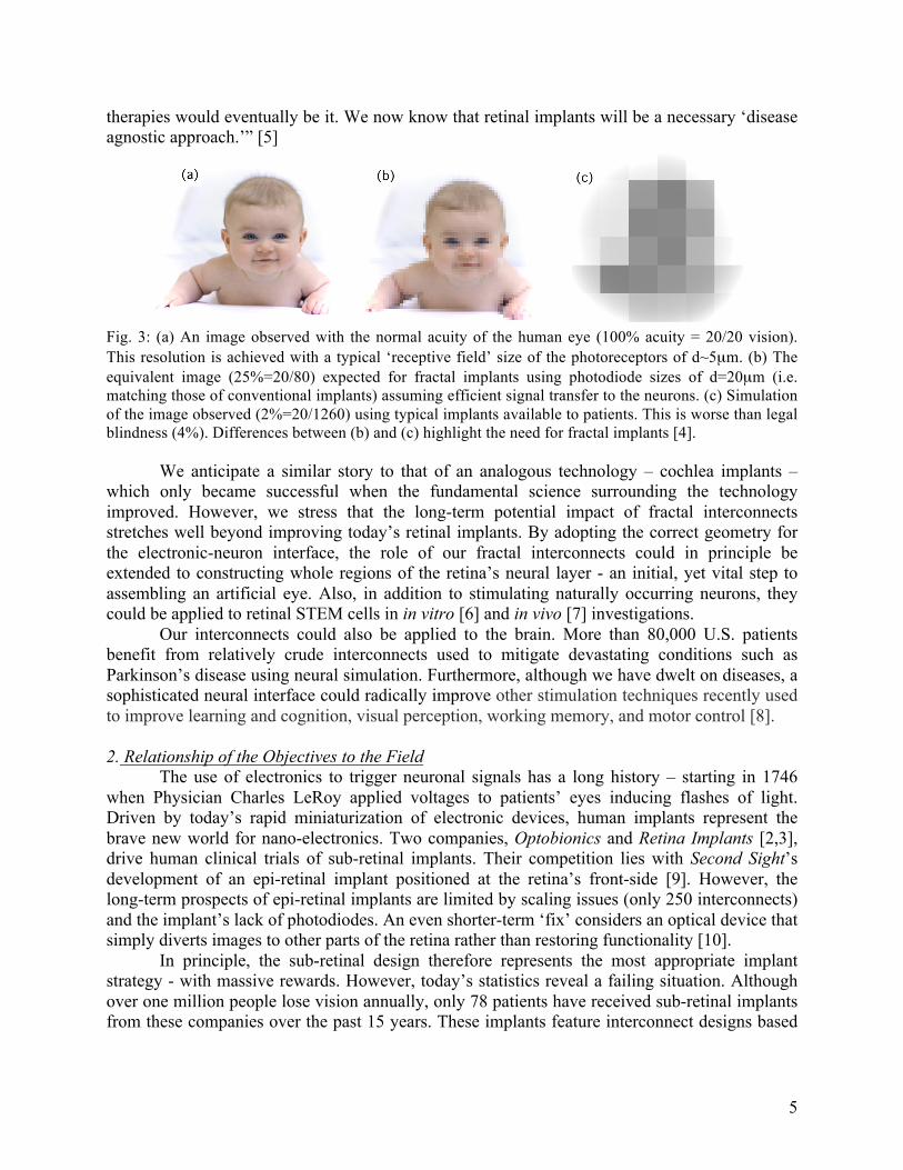
Fig. 2: (a) Side view of the eye showing the sub-retinal implant (black) replacing diseased photoreceptors in the retinal region immediately behind the neural layer (red). (b) Side view of a photodiode and associated electronics (blue), which receives light and then charges the interconnect (grey). The generated voltage V drops off with distance from the interconnect (red = -0.5V, mauve = 0V). To defeat screening of this voltage by ions in the eye fluid, the electronics oscillates V at kHz frequencies. The neuron will be stimulated if located close enough to experience the voltage. (c) Schematic showing a traditional design, featuring a 20µm by 20µm photodiode with a square-shaped interconnect. (d) Our equivalent design, featuring an interconnect with fractal branches. Typical implants feature an array of 2000-5000 components (i.e. photodiode plus interconnect) fabricated on a 2-3mm chip. The interconnects are intrinsically multi-functional. Their optical properties dictate the amount of the light entering from the eye into the photodiodes (setting the light sensitivity) and also their wavelengths (setting color). Their optical and electrical properties combine to determine how much potentially harmful heat is generated. The electrical properties also determine the distance that the voltages extend from the implant into the retina’s neural layer (with larger distances increasing the likelihood of stimulation). Their physical properties determine whether the neurons stay close enough to the interconnect to experience these voltages. Our preliminary investigations indicate that a bio-inspired fractal interconnect will radically improve all 4 properties (optical, electrical, thermal, and physical) of the implant - with the ‘game changing’ consequences shown in Fig. 3. The target visual acuity for fractal implants is 25% of the normal eye’s acuity (Fig. 3b). This compares to the 2% estimated for typical implants currently available to patients (Fig. 3c). Ophthalmology Professor Tim Stout, a specialist in eye diseases, noted of our fractal implant designs: “Surgeons will bend over backwards to put in place the best solution … 5 years ago we might have concluded that gene
5
therapies would eventually be it. We now know that retinal implants will be a necessary ‘disease agnostic approach.’” [5]
Fig. 3: (a) An image observed with the normal acuity of the human eye (100% acuity = 20/20 vision). This resolution is achieved with a typical ‘receptive field’ size of the photoreceptors of d~5µm. (b) The equivalent image (25%=20/80) expected for fractal implants using photodiode sizes of d=20µm (i.e. matching those of conventional implants) assuming efficient signal transfer to the neurons. (c) Simulation of the image observed (2%=20/1260) using typical implants available to patients. This is worse than legal blindness (4%). Differences between (b) and (c) highlight the need for fractal implants [4]. We anticipate a similar story to that of an analogous technology – cochlea implants – which only became successful when the fundamental science surrounding the technology improved. However, we stress that the long-term potential impact of fractal interconnects stretches well beyond improving today’s retinal implants. By adopting the correct geometry for the electronic-neuron interface, the role of our fractal interconnects could in principle be extended to constructing whole regions of the retina’s neural layer - an initial, yet vital step to assembling an artificial eye. Also, in addition to stimulating naturally occurring neurons, they could be applied to retinal STEM cells in in vitro [6] and in vivo [7] investigations. Our interconnects could also be applied to the brain. More than 80,000 U.S. patients benefit from relatively crude interconnects used to mitigate devastating conditions such as Parkinson’s disease using neural simulation. Furthermore, although we have dwelt on diseases, a sophisticated neural interface could radically improve other stimulation techniques recently used to improve learning and cognition, visual perception, working memory, and motor control [8]. 2. Relationship of the Objectives to the Field The use of electronics to trigger neuronal signals has a long history – starting in 1746 when Physician Charles LeRoy applied voltages to patients’ eyes inducing flashes of light. Driven by today’s rapid miniaturization of electronic devices, human implants represent the brave new world for nano-electronics. Two companies, Optobionics and Retina Implants [2,3], drive human clinical trials of sub-retinal implants. Their competition lies with Second Sight’s development of an epi-retinal implant positioned at the retina’s front-side [9]. However, the long-term prospects of epi-retinal implants are limited by scaling issues (only 250 interconnects) and the implant’s lack of photodiodes. An even shorter-term ‘fix’ considers an optical device that simply diverts images to other parts of the retina rather than restoring functionality [10]. In principle, the sub-retinal design therefore represents the most appropriate implant strategy - with massive rewards. However, today’s statistics reveal a failing situation. Although over one million people lose vision annually, only 78 patients have received sub-retinal implants from these companies over the past 15 years. These implants feature interconnect designs based
6
on computing and communications applications. Unfortunately, these smooth, solid shapes (Fig. 2c) represent a fundamentally flawed geometry for interfacing with neurons. Firstly, these interconnects block much of the light entering the photodiode. Secondly, the stimulating voltage falls off rapidly with distance. Thirdly, their smoothness is foreign to the neurons, triggering the formation of a ‘scar’ layer of glial cells. Glial cells function as the life-support system for neurons and this protective layer distances the neurons from the foreign surface [11]. However, pushing the neurons away limits stimulation [11]. These factors combine to deliver a devastating blow to performance. One strategy to improve performance increases the number of photodiodes per pixel site. But this has the significant disadvantage of increasing the size of each site from 20µm to 150µm (reducing acuity by a factor of 10) [12]. In 2013, the UO granted an Incubation Award to the research team to fund a one-year investigation of bio-inspired fractal interconnects. Preliminary results (see Methodology Section 3 for details) demonstrated the team’s ability to fabricate fractal interconnects and simulate their neural stimulation. Crucially, initial in vitro experiments also revealed that neurons adhere to the interconnects’ fractal branches. Taylor was awarded a Pufendorf Fellowship in 2014 to collaborate with adhesion experts at Lund University and his 3-month visit to Lund with 3 UO students started the transfer of these skills to UO. Previous experiments performed by our Lund collaborators and others highlight the importance of textured surfaces for encouraging neuron adhesion e.g. [13-17] and reducing glial scars [18]. Only 20% of neurons adhere to smooth metallic interconnects [19] while experiments on textured metallic interconnects indicate 25% [13]. None took the vital step of matching the texture pattern to that of the neurons’ fractal branches to improve adhesion. Nor did they consider the interdependence of the physical (i.e. adhesive), optical, electrical, and thermal properties of the neuron-implant interface. In contrast, we will adopt the integrative approach required for success. A striking example concerns the recent experiments (unrelated to implants) demonstrating that fractal branches efficiently filter light [20]. Similarly, fractal circuits were recently proposed for stretchable electronics [21] – the associated flexibility will be ideal for our implants. We plan to exploit and develop these recent discoveries and combine them with our results highlighting the advantageous electrical, thermal, and selective adhesion properties of fractals. Adopting the philosophy that the implant is only as strong as its weakest link, we will target the fundamental science that emerges when all of these processes are considered in unison. Although our proposal targets novel geometry, it builds on previous investigations of materials designed to interface with neurons. Accordingly, our fabrication methods will exploit established materials - TiN and carbon nanotubes. TiN research demonstrates stability over long periods of continuous stimulation both in vitro and in vivo [22]. In vitro cultures on TiN also reveal that it is not cytotoxic [19]. Furthermore, subretinal implants in humans have already used TiN [3]. A large body of research has investigated carbon nanotubes e.g. [16-17, 23-26]. Nanotube networks will make ideal materials for flexible fractal interconnects because of their unique properties [27]. In particular, nanotubes have excellent electrical current capacity (1000 times that of copper), they can be made semiconducting or metallic with carrier mobilities better than silicon, and they are incredibly strong (100 times stronger than high-grade steal). Yet they are tremendously flexible and can deform and buckle elastically [28]. Furthermore, nanotubes adhere tremendously well to both solid substrates (binding energies of a few eV/Å) [29] and living cells [30], and can be synthesized to be nontoxic [31]. Thus, the biocompatibility, flexibility, strength, tunable electrical conductivity of nanotubes and the superior adhesion properties on biological systems make them ideal for neuron-interfaced fractal interconnects. For
7
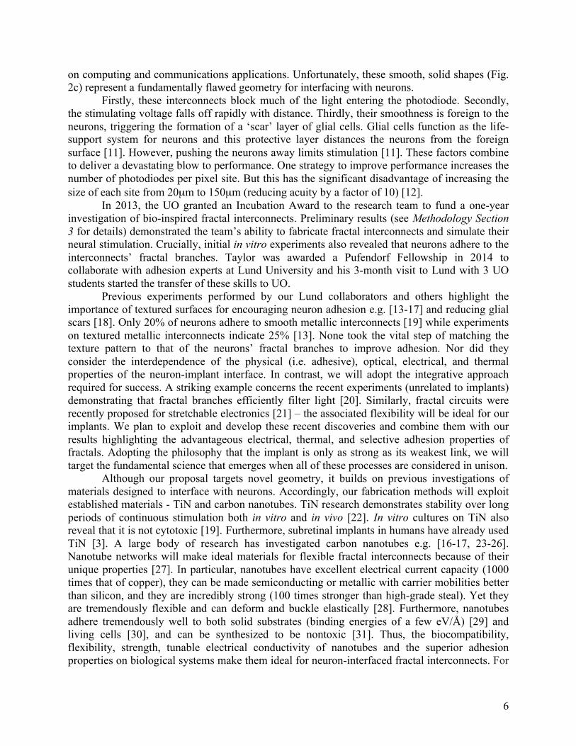
both material systems, we will also exploit studies showing that functionalising the surface improves the survival rate and adhesion of the neurons [22]. Examples include nanowire textures [15], homopolymer poly-L-lysine for TiN [22] and pyrene for the nanotubes [32]. 3. Proposed Methodology and Procedures 3.1 Fabrication of Interconnects Three novel fabrication techniques will be developed, each designed to match specific fractal characteristics of the interconnects to those of the neurons. For each system, the fractal interconnects will ultimately feature branch sizes spanning from 25µm down to 50nm. Whereas all fractals exhibit repetition of patterns at increasingly fine scales, fractals can be grouped into 2 categories based on how the patterns repeat. For fractals prevalent in nature, in particular in the body (e.g. neurons, veins, bronchial trees), the statistical qualities of the patterns repeat at different size scales. In contrast, the patterns of mathematically-generated ‘exact’ fractals repeat exactly at different scales. Consequently, whereas exact fractals look precisely the same at increasingly fine scales, ‘statistical’ fractals simply look similar at different scales [33]. One of our fabrication techniques will exploit the precision and control associated with the ‘clean’ geometry of exact fractals. The others will adopt novel self-assembly fabrication methods to harness natural growth processes that generate statistical fractals. A central parameter for quantifying fractals is their fractal dimension D. This describes how the patterns occurring at different magnifications combine to build the resulting fractal shape [34]. For Euclidean shapes, dimension is described by familiar integer values – for a smooth line D = 1, whilst for a completely filled area D = 2. However, the repeating patterns of a fractal line cause the line to begin to occupy space. Consequently, its D value lies between 1 and 2. Fig. 4 (a,b) shows the result of adjusting D for the branches of our fractal interconnects. For each of the fabrication techniques, D will be adjusted along with the number of repeating iterations to investigate their impact on the adhesive, electrical, thermal, and optical properties.
Fig. 4. (a,b) Demonstration of D’s impact on the ‘H tree’ fractal shape. 3 iterations (red, green, blue) are shown. Note how the fractal patterns decrease at a higher rate for D = 1.1 (a) than for D = 1.9 (b). (c,d) Scanning electron micrographs (SEMs) of example interconnects featuring D = 1.5 fractal branches. Johnson and Taylor’s groups will fabricate interconnects based on exact fractals using techniques recently refined in a collaboration with the UO Center for Sustainable Materials Chemistry. Two lithographic resists (SU-8 and HafSOx) [35] will be used depending on the feature sizes required. Both resists are known to be biocompatible with neurons. Collaborating with the Lund experts, Taylor’s group performed initial neural adhesion tests on both resists (see Section 3.2). Figs. 4 (c, d) show fractals defined in a SU-8 resist with feature sizes spanning from 500µm to 2 µm. Optical lithography is used to define this resist pattern, which can then be transferred to TiN using electron-beam evaporation and a ‘lift-off’ technique. The HafSOx resist can produce patterns from 450 µm down to extremely small sizes of 21nm, spanning 9 iterations.
8
Electron-beam lithography is used to pattern the resist. The exposed HafSOx then acts as a mask for an electron milling process that defines the pattern in an underlying TiN layer.
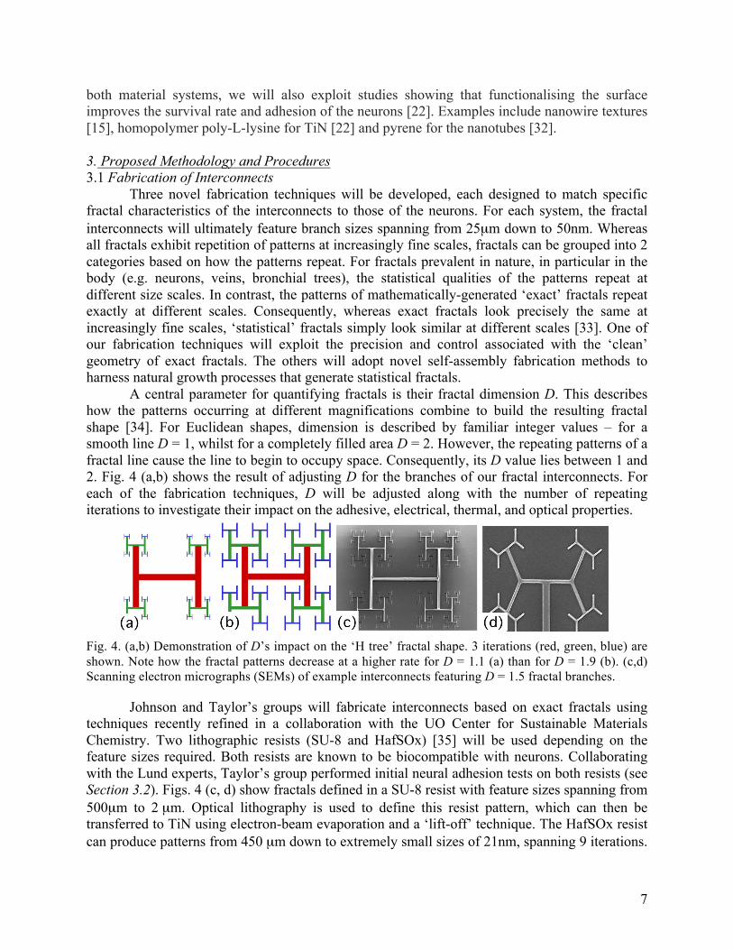
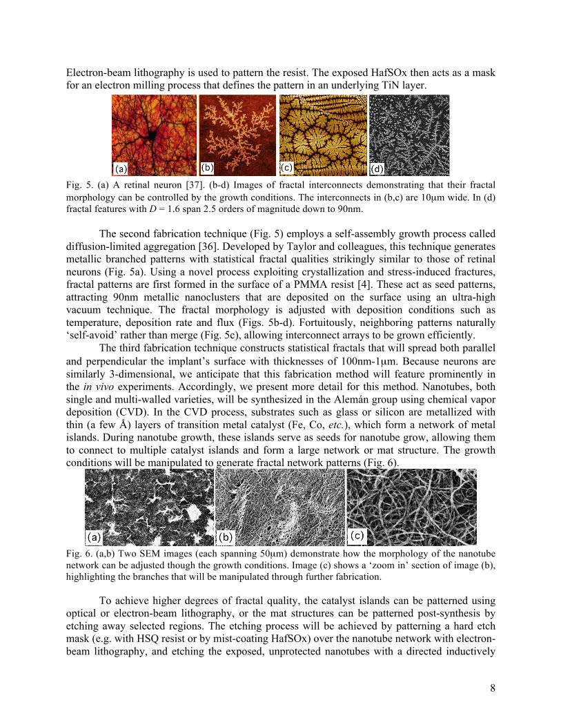
Fig. 5. (a) A retinal neuron [37]. (b-d) Images of fractal interconnects demonstrating that their fractal morphology can be controlled by the growth conditions. The interconnects in (b,c) are 10µm wide. In (d) fractal features with D = 1.6 span 2.5 orders of magnitude down to 90nm. The second fabrication technique (Fig. 5) employs a self-assembly growth process called diffusion-limited aggregation [36]. Developed by Taylor and colleagues, this technique generates metallic branched patterns with statistical fractal qualities strikingly similar to those of retinal neurons (Fig. 5a). Using a novel process exploiting crystallization and stress-induced fractures, fractal patterns are first formed in the surface of a PMMA resist [4]. These act as seed patterns, attracting 90nm metallic nanoclusters that are deposited on the surface using an ultra-high vacuum technique. The fractal morphology is adjusted with deposition conditions such as temperature, deposition rate and flux (Figs. 5b-d). Fortuitously, neighboring patterns naturally ‘self-avoid’ rather than merge (Fig. 5c), allowing interconnect arrays to be grown efficiently. The third fabrication technique constructs statistical fractals that will spread both parallel and perpendicular the implant’s surface with thicknesses of 100nm-1µm. Because neurons are similarly 3-dimensional, we anticipate that this fabrication method will feature prominently in the in vivo experiments. Accordingly, we present more detail for this method. Nanotubes, both single and multi-walled varieties, will be synthesized in the Alemán group using chemical vapor deposition (CVD). In the CVD process, substrates such as glass or silicon are metallized with thin (a few Å) layers of transition metal catalyst (Fe, Co, etc.), which form a network of metal islands. During nanotube growth, these islands serve as seeds for nanotube grow, allowing them to connect to multiple catalyst islands and form a large network or mat structure. The growth conditions will be manipulated to generate fractal network patterns (Fig. 6).
Fig. 6. (a,b) Two SEM images (each spanning 50µm) demonstrate how the morphology of the nanotube network can be adjusted though the growth conditions. Image (c) shows a ‘zoom in’ section of image (b), highlighting the branches that will be manipulated through further fabrication. To achieve higher degrees of fractal quality, the catalyst islands can be patterned using optical or electron-beam lithography, or the mat structures can be patterned post-synthesis by etching away selected regions. The etching process will be achieved by patterning a hard etch mask (e.g. with HSQ resist or by mist-coating HafSOx) over the nanotube network with electron-beam lithography, and etching the exposed, unprotected nanotubes with a directed inductively
9
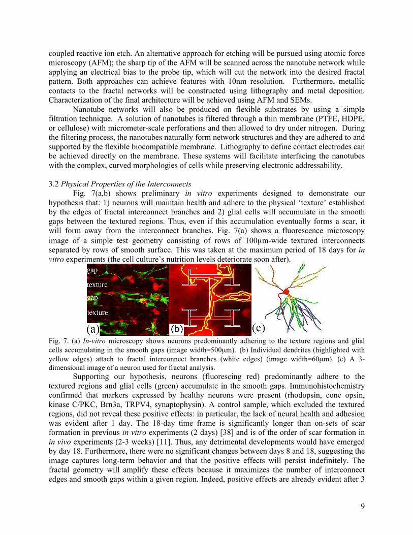
coupled reactive ion etch. An alternative approach for etching will be pursued using atomic force microscopy (AFM); the sharp tip of the AFM will be scanned across the nanotube network while applying an electrical bias to the probe tip, which will cut the network into the desired fractal pattern. Both approaches can achieve features with 10nm resolution. Furthermore, metallic contacts to the fractal networks will be constructed using lithography and metal deposition. Characterization of the final architecture will be achieved using AFM and SEMs. Nanotube networks will also be produced on flexible substrates by using a simple filtration technique. A solution of nanotubes is filtered through a thin membrane (PTFE, HDPE, or cellulose) with micrometer-scale perforations and then allowed to dry under nitrogen. During the filtering process, the nanotubes naturally form network structures and they are adhered to and supported by the flexible biocompatible membrane. Lithography to define contact electrodes can be achieved directly on the membrane. These systems will facilitate interfacing the nanotubes with the complex, curved morphologies of cells while preserving electronic addressability. 3.2 Physical Properties of the Interconnects Fig. 7(a,b) shows preliminary in vitro experiments designed to demonstrate our hypothesis that: 1) neurons will maintain health and adhere to the physical ‘texture’ established by the edges of fractal interconnect branches and 2) glial cells will accumulate in the smooth gaps between the textured regions. Thus, even if this accumulation eventually forms a scar, it will form away from the interconnect branches. Fig. 7(a) shows a fluorescence microscopy image of a simple test geometry consisting of rows of 100µm-wide textured interconnects separated by rows of smooth surface. This was taken at the maximum period of 18 days for in vitro experiments (the cell culture’s nutrition levels deteriorate soon after).
Fig. 7. (a) In-vitro microscopy shows neurons predominantly adhering to the texture regions and glial cells accumulating in the smooth gaps (image width=500µm). (b) Individual dendrites (highlighted with yellow edges) attach to fractal interconnect branches (white edges) (image width=60µm). (c) A 3-dimensional image of a neuron used for fractal analysis. Supporting our hypothesis, neurons (fluorescing red) predominantly adhere to the textured regions and glial cells (green) accumulate in the smooth gaps. Immunohistochemistry confirmed that markers expressed by healthy neurons were present (rhodopsin, cone opsin, kinase C/PKC, Brn3a, TRPV4, synaptophysin). A control sample, which excluded the textured regions, did not reveal these positive effects: in particular, the lack of neural health and adhesion was evident after 1 day. The 18-day time frame is significantly longer than on-sets of scar formation in previous in vitro experiments (2 days) [38] and is of the order of scar formation in in vivo experiments (2-3 weeks) [11]. Thus, any detrimental developments would have emerged by day 18. Furthermore, there were no significant changes between days 8 and 18, suggesting the image captures long-term behavior and that the positive effects will persist indefinitely. The fractal geometry will amplify these effects because it maximizes the number of interconnect edges and smooth gaps within a given region. Indeed, positive effects are already evident after 3
10
days in culture: the zoom-in of Fig. 7(b) shows adhesion of individual dendrites to the fractal interconnect branches of Fig. 4(c) (note also the lack of glial cell accumulation in the smooth gaps between the branches at this early stage). The long-term goal is for this ‘one-to-one’ adhesion to occur for the hundreds of branches in each fractal interconnect. Taylor’s group will use fluorescence microscopy to correlate variables such as neuron cell count, number of dendrites and dendrite length with the fractal properties of the 3 types of fractal interconnect. Automated procedures will be developed to quantify these variables, along with software for matching the dendrite patterns to the underlying interconnects. Building on the initial experimental designs [39], retinal neurons will be cultured from neonatal mice. The retina will be removed from the outer epithelium and placed in culture medium, which will be mechanically agitated to separate the neurons. These will be filtered out and stained with DAPI, GFAP, and β-tubulin III. This staining allows the retinal components to be analyzed separately. DAPI fluoresces blue and fixes to both glia and neuron cell nuclei (allowing a total cell count), GFAP fluoresces green and attaches to glia cells, and β-tubulin III fluoresces red and binds to neuron microtubules. Whereas this study of dissociated retinal cells is necessary for initial parameter characterization, a “retinal explant” will also be used. The retina will be dissected and cultured as a whole “intact” system. This will be more relevant to the conditions in the in vivo experiments. Precision imaging will be possible by fabricating interconnects on glass substrates. Analysing the neuron shapes is vital for understanding the neuron-interconnect interface. Previous research of neuron geometry used fractal analysis simply as a tool for quantifying their structural complexity. In contrast, Taylor recently used confocal microscopy to construct 3-dimensional images of neurons, allowing the first investigation of the origin of neurons’ fractal character (Fig. 7c). Strikingly, this character originates from the way dendrites ‘weave’ though space. This has crucial consequences because adhesion experiments reveal that this weave is forced to change as neurons interact with surfaces. Our hypothesis predicts superior adhesion when the fractal characteristics (in particular D and branch orientation (Fig. 4(d)) of the interconnect and neuron are matched. This will occur because the dendrites can connect without having to adjust their fractal characteristics. This effect is an example of ‘fractal geometric resonance’ in which interface properties are enhanced by matching the geometric properties of two fractals. Because different neuron types are expected to have specific weaves [40], ‘selective adhesion’ should be possible - whereby specific neurons adhere to targeted interconnects based on their precise fractal characteristics. This is important for color vision where, for example, the blue photodiode (filtered to receive blue light) will connect to a blue bipolar neuron. 3.3 Electrical Properties of the Interconnects Taylor’s group is developing computer simulations to quantify the fractal interconnect’s superior neural stimulation compared to conventional square interconnects (Fig. 8). Initial focus has been on exact fractals but this will be extended to the more complex statistical fractals. An ‘equivalent circuit’ is used to model the interconnect, neuron and surrounding liquid. This intricate circuit features a 3-dimensional array of resistive and capacitive components based on realistic conditions [41], incorporating screening ions in the liquid and also the electrochemistry induced at the interconnect surface. Equations based on modified nodal analysis then quantify the circuit’s behavior [42-44]. This represents a huge computation challenge due to: 1) the interconnects intricate fractal patterns (1.5 million node voltages are solved compared to 20 thousand nodes in previous studies [45]), and 2) the voltage’s dynamic quality (recall that this voltage oscillates at kHz frequencies to defeat ion screening and also to refresh the neuron).
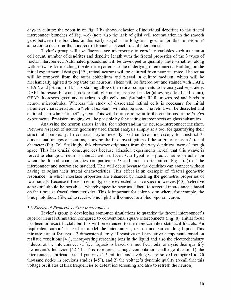
11
Fig. 8. (a,b) Charge density maps showing high densities (light blue) accumulating at the boundaries for both the square (a) and the fractal (b) TiN interconnects. (c,d) Voltage maps (red = -0.5V, dark blue = 0V) for the top views of the square (c) and fractal (d) interconnects. The equivalent side views are shown in (e,f). The computed internal signal voltage of the neuron is shown in (g) (yellow = high, brown = low). Initial simulations reveal that charge accumulates on the outer boundaries of the interconnect (Fig. 8a,b). This generates a remarkable ‘Faraday effect’ in which the voltage ‘spreads’ across the gaps between the repeating branches of the fractal interconnect (Fig. 8c,d). Consequently, these gaps do not degrade the voltages generated. Considering square and fractal interconnects where the total number of covered surface pixels is identical, the gaps allow the fractal interconnects (and the associated voltage) to spread over a larger region. Fig. 8(e,f) shows that the voltage from the fractal interconnect then penetrates further into the liquid. In Fig. 8(g), a model neuron (~100µm long) is inserted into the simulated voltages in order to quantify the larger number of signals induced in the neuron by the fractal interconnects. This conversion from extracellular to internal voltage signal is computed using equivalent circuit components that model the neuron’s membrane and its internal resistance [46]. Preliminary results emphasize the crucial role of neural adhesion. Voltages generated by conventional squares decrease by 90% at a 10µm distance from the interconnect. Glial scars can push the neurons 50µm away where V=0.
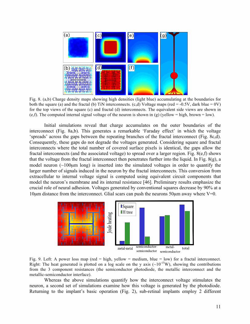
Fig. 9. Left: A power loss map (red = high, yellow = medium, blue = low) for a fractal interconnect. Right: The heat generated is plotted on a log scale on the y axis (~10-15W), showing the contributions from the 3 component resistances (the semiconductor photodiode, the metallic interconnect and the metallic-semiconductor interface). Whereas the above simulations quantify how the interconnect voltage stimulates the neuron, a second set of simulations examine how this voltage is generated by the photodiode. Returning to the implant’s basic operation (Fig. 2), sub-retinal implants employ 2 different
12
methods for converting light into a voltage. Some implants operate in the ‘open circuit’ mode, in which the photodiode directly charges the interconnect [2]. Alternatively, in the ‘short circuit’ mode the current from the photodiode flows through an ammeter. This then signals a voltage generator to charge the interconnect [3]. The interconnect’s shape drastically affects both modes because it dictates the electrical resistance. For example, in the ‘open circuit’ mode, a high resistance reduces the current, resulting in low sensitivity of the implant to light. More crucially, the lost current energy is converted into heat, which is undesirable for the eye’s health. Taylor’s group is developing equivalent circuit simulations for the ‘short-circuit mode’ [4]. Preliminary results in Fig. 9(right) suggest that fractal interconnects (green) can reduce the current’s heating compared to the conventional squares (blue). Future studies, including more intricate statistical fractals, will examine how adjustments to the fractal shapes can further minimize heating.
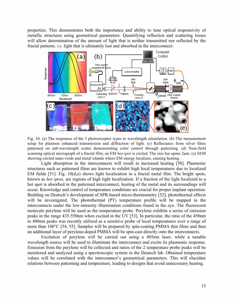
3.4 Optical Properties of the Interconnects The surface density of fractal interconnects is less than the squares due to the multitude of gaps between the branches. Adopting a simple pixel count, this suggests high light transmission into the photodiode. However, in contrast to the square, some fractal feature sizes are comparable to, or smaller than, the light’s wavelength. This raises the possibility of manipulating feature sizes to investigate whether light transmission can be tuned based on wavelength through diffractive and plasmonic effects. If so, the fractal interconnects could serve as color filters. In particular, they might be designed to match the 3 photoreceptor types used for color vision (the RGB cones in Fig. 10a), leading to the first implants capable of color vision. Metallic systems with interfaces patterned on subwavelength scales support localized surface plasmons - coupled modes of charge density waves (plasmons) and photons - excited when electromagnetic (EM) radiation impinges on the interface [47]. Unlike bulk metals, the surface plasmon resonance (SPR) of patterned systems such as fractals is a unique, sensitive function of the system’s shape, size and composition [48]. Significant recent progress has been made in understanding SPR phenomena in metallic films including regular and fractal patterned films [49]. Deutsch’s group will build on this knowledge to investigate the optical properties of the fractal interconnects. Quantifying the optical energy losses and their relation to structural parameters will allow unwanted optical losses and heat generation to be minimized. Previous studies of patterned conducting films established their tendency to enhance transmittance of optical signals at select portions of the spectrum. Known as plasmon-assisted extraordinary transmission, this is enabled by the ‘antenna effect’ in metal films patterned on wavelength scales, and is manifest as greatly enhanced coupling of energy across the film into both specular and diffracted modes. Deutsch will measure the plasmon enhanced transmission and diffraction of light impinging on the interconnects (Fig. 10(b)). Transmission and diffraction efficiencies will be determined as a function of the interconnects’ geometrical parameters and will be used to optimize designs that maximize light transmittance and enable color filtering. Diffuse and specular reflected light signals will be measured (Fig. 10(b)). Patterned metal films are known to strongly scatter light due to the very large scattering cross sections of their sub-wavelength sized features. It is crucial to quantify the optical scattering of the interconnects, since scattered light will lead to reduced perceived visual signals, i.e. reduced visibility, blurring, and loss of contrast. Patterned interconnects will be placed in the light beam path and angular scans of the reflected light will be collected. Fig. 10(c) shows white-light reflectance from 50nm thick silver films patterned on sub-wavelength scales at 3 different periodicities. It is clear that only slight variations in the films’ structure results in striking differences in their optical
13
properties. This demonstrates both the importance and ability to tune optical responsivity of metallic structures using geometrical parameters. Quantifying reflection and scattering losses will allow determination of the amount of light that is neither transmitted nor reflected by the fractal patterns. i.e. light that is ultimately lost and absorbed in the interconnect.
Fig. 10. (a) The responses of the 3 photoreceptor types to wavelength stimulation. (b) The measurement setup for plasmon enhanced transmission and diffraction of light. (c) Reflectance from silver films patterned on sub-wavelength scales demonstrating color control through patterning. (d) Near-field scanning optical micrograph of a fractal film; an EM hot-spot is circled. The size bar spans 2µm. (e) SEM showing circled nano-voids and metal islands where EM energy localizes, causing heating. Light absorption in the interconnects will result in increased heating [50]. Plasmonic structures such as patterned films are known to exhibit high local temperatures due to localized EM fields [51]. Fig. 10(d,e) shows light localization in a fractal metal film. The bright spots, known as hot spots, are regions of high light localization. If a fraction of the light localized to a hot spot is absorbed in the patterned interconnect, heating of the metal and its surroundings will occur. Knowledge and control of temperature conditions are crucial for proper implant operation. Building on Deutsch’s development of SPR-based micro-thermometry [52], photothermal effects will be investigated. The photothermal (PT) temperature profile will be mapped in the interconnects under the low-intensity illumination conditions found in the eye. The fluorescent molecule perylene will be used as the temperature probe. Perylene exhibits a series of emission peaks in the range 435-550nm when excited in the UV [53]. In particular, the ratio of the 450nm to 480nm peaks was recently utilized as a sensitive probe of local temperatures over a range of more than 100°C [54, 55]. Samples will be prepared by spin-coating PMMA thin films and then an additional layer of perylene-doped PMMA will be spin-cast directly onto the interconnects. Excitation of perylene will be carried out using a 405nm laser, while a tunable wavelength source will be used to illuminate the interconnect and excite its plasmonic response. Emission from the perylene will be collected and ratios of the 2 temperature probe peaks will be monitored and analyzed using a spectroscopic system in the Deutsch lab. Obtained temperature values will be correlated with the interconnect’s geometrical parameters. This will elucidate relations between patterning and temperature, leading to designs that avoid unnecessary heating.
14
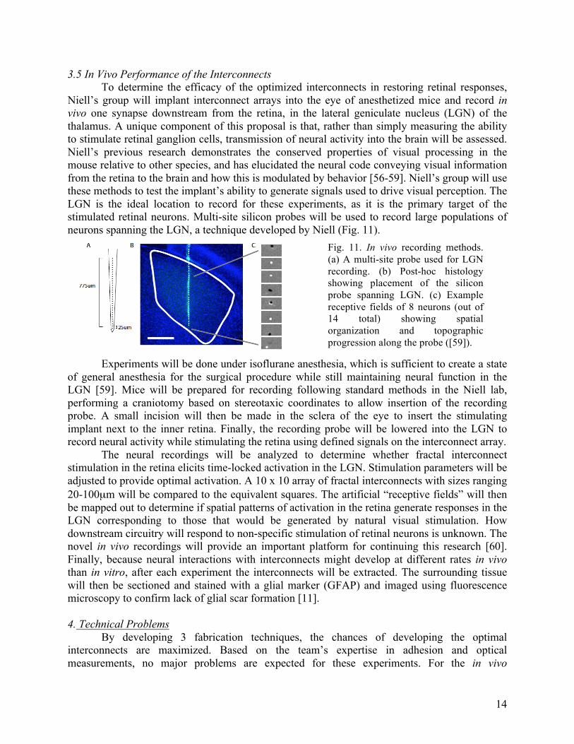
3.5 In Vivo Performance of the Interconnects To determine the efficacy of the optimized interconnects in restoring retinal responses, Niell’s group will implant interconnect arrays into the eye of anesthetized mice and record in vivo one synapse downstream from the retina, in the lateral geniculate nucleus (LGN) of the thalamus. A unique component of this proposal is that, rather than simply measuring the ability to stimulate retinal ganglion cells, transmission of neural activity into the brain will be assessed. Niell’s previous research demonstrates the conserved properties of visual processing in the mouse relative to other species, and has elucidated the neural code conveying visual information from the retina to the brain and how this is modulated by behavior [56-59]. Niell’s group will use these methods to test the implant’s ability to generate signals used to drive visual perception. The LGN is the ideal location to record for these experiments, as it is the primary target of the stimulated retinal neurons. Multi-site silicon probes will be used to record large populations of neurons spanning the LGN, a technique developed by Niell (Fig. 11).
Experiments will be done under isoflurane anesthesia, which is sufficient to create a state of general anesthesia for the surgical procedure while still maintaining neural function in the LGN [59]. Mice will be prepared for recording following standard methods in the Niell lab, performing a craniotomy based on stereotaxic coordinates to allow insertion of the recording probe. A small incision will then be made in the sclera of the eye to insert the stimulating implant next to the inner retina. Finally, the recording probe will be lowered into the LGN to record neural activity while stimulating the retina using defined signals on the interconnect array. The neural recordings will be analyzed to determine whether fractal interconnect stimulation in the retina elicits time-locked activation in the LGN. Stimulation parameters will be adjusted to provide optimal activation. A 10 x 10 array of fractal interconnects with sizes ranging 20-100µm will be compared to the equivalent squares. The artificial “receptive fields” will then be mapped out to determine if spatial patterns of activation in the retina generate responses in the LGN corresponding to those that would be generated by natural visual stimulation. How downstream circuitry will respond to non-specific stimulation of retinal neurons is unknown. The novel in vivo recordings will provide an important platform for continuing this research [60]. Finally, because neural interactions with interconnects might develop at different rates in vivo than in vitro, after each experiment the interconnects will be extracted. The surrounding tissue will then be sectioned and stained with a glial marker (GFAP) and imaged using fluorescence microscopy to confirm lack of glial scar formation [11]. 4. Technical Problems By developing 3 fabrication techniques, the chances of developing the optimal interconnects are maximized. Based on the team’s expertise in adhesion and optical measurements, no major problems are expected for these experiments. For the in vivo
Fig. 11. In vivo recording methods. (a) A multi-site probe used for LGN recording. (b) Post-hoc histology showing placement of the silicon probe spanning LGN. (c) Example receptive fields of 8 neurons (out of 14 total) showing spatial organization and topographic progression along the probe ([59]).
15
experiments, it’s possible that the small size of the mouse eye will be problematic for implant insertion, although other groups have demonstrated the ability to perform sub-retinal implant in mice [61]. However, if this proves challenging we will translate our experiments to the rat, which has ~2x diameter eye. Niell has experience with similar recording methods in rats. 5. Facilities/Research Environment The UO is an ideal environment – the team builds on the expertise within 3 departments (Physics, Chemistry and Biochemistry, Biology) and 4 institutes/centers (Materials Science Institute, Institute of Neuroscience, Oregon Center for Optics, and The Center for Sustainable Materials Chemistry). The UO has a tradition for interdisciplinary research. The project’s flow line (Fig. 1) will encourage interdisciplinary activity at the faculty and student levels. Fabrication will occur in the Lokey Laboratories, which contains $25M of high-performance equipment. Embedded in a 17ft deep bedrock vault, the low noise/low vibration environment is ideal for our fabrication. Alemán’s laboratory was recently renovated specifically for nanotube fabrication and measurement. It houses a CVD furnace, spin coater, mask aligner, and a Class 0 cleanroom wet chemistry processing station. The AALAC accredited Transgenic Mouse Facility (previously funded by WMKF) will be used for in vivo experiments. The new UO supercomputing cluster will be used for simulations. Major equipment is in place for the experiments on in vitro adhesion (e.g wet-benches, optical microscopes including a confocal) and optical properties (e.g. tunable white light source, lasers, 2 spectrometers, an inverted epiflourescence microscope, access to a UV-Vis system and cost-based access to NSOM). We have applied to the NSF for an AFM for imaging and fabrication. If unsuccessful, we will use the Lokey facility’s existing AFM. We are developing a $50k request to the Steven A. Wynn Foundation for dedicated in vivo equipment. If unsuccessful, we will use the existing 2 extracellular recording systems with the multiple stereotaxis surgical stations that are in place for the in vivo experiments. 6. Future Plans The WMKF proposal focuses on retinal implants. Given the team’s expertise, the 3-year time frame is realistic for demonstrating the superior performance of the fractal interconnects in the visual system of mice. The ultimate goal, however, is to restore vision in humans to the level shown in Fig. 3. This future phase will involve an integration of the fundamental science discovered in the WMKF project with engineering (e.g. fabricating a 2-3 mm chip featuring arrays of 2000-5000 components) and medical (e.g. human clinical trials) considerations. We also plan to expand beyond the retinal focus of the current proposal. Our generic interconnects can be used for interfacing with a range of neurons in the body. Furthermore, the current proposal employs fractal interconnects for stimulating signals in neurons. Some of the favourable properties (such as enhanced neural adhesion) could improve electronic sensors used to detect neural signals. For example, although detection of 10000s of neural signals will be needed to study brain behavior, today’s electronic sensors can only track less than 100 simultaneously. One reason for this poor performance is that many neurons lie too far from the sensor to be detected – adhesion would make the neurons stay within detectable range. ‘Selective adhesion’ could also be used to link neurons together into artificially designed neural networks, allowing simpler networks to be studied alongside the more complex natural ones. Given the wealth of potential fundamental and applied research of our fractal interconnects, the team plans to leverage the results generated during the WMKF project to establish a multidisciplinary center at the UO (funded, for example, by the NSF Materials Research Science and Engineering Center scheme).
16
7. References/Bibliography [1] Taylor, R.P. “Artificial Vision” Physics World 24 (2011): 22-25. [2] See the Optobionics website: http://optobionics.com/. [3] See the Retina Implant website: http://www.retina-implant.de/en/default.aspx. [4] Montgomery, R.D. Fractal Electronics for Interfacing Neurons to Retinal Implants, Ph.D.
thesis, University of Oregon, 2014. [5] Professor Stout (Baylor College of Medicine, USA) was interviewed as part of the University
of Oregon's Technology Entrepreneurship Program. [6] Eiraku, M. et al "Self-organizing optic-cup morphogenesis in three-dimensional culture"
Nature 472.7341 (2011): 51-56. [7] See: http://www.nature.com/news/japanese-woman-is-first-recipient-of-next-generation-
stem-cells-1.15915. [8] Fox, D. "Brain Buzz" Nature News 472.7342 (2011): 156-159. [9] See Second Sight’s website: http://www.2-sight.com. [10] See U.C. Davies’s website: http://www.ucdmc.ucdavis.edu/publish/news/newsroom/6949. [11] Polikov, V. S. et al "Response of brain tissue to chronically implanted neural electrodes"
Journal of Neuroscience Methods 148.1 (2005): 1-18. [12] Wang, L. et al "Photovoltaic retinal prosthesis: implant fabrication and performance"
Journal of Neural Engineering 9.4 (2012): 046014. [13] Collazos-Castro, J. E. et al "Neural cell growth on TiO 2 anatase nanostructured surfaces"
Thin Solid Films 518.1 (2009): 160-170. [14] David-Pur, M. et al "All-carbon-nanotube flexible multi-electrode array for neuronal
recording and stimulation" Biomedical microdevices 16.1 (2014): 43-53. [15] Hällström, W. et al "Gallium phosphide nanowires as a substrate for cultured neurons" Nano
letters 7.10 (2007): 2960-2965. [16] Mattson, M.P. et al "Molecular functionalization of carbon nanotubes and use as substrates
for neuronal growth" Journal of Molecular Neuroscience 14.3 (2000): 175-182. [17] Lovat, V. et al "Carbon nanotube substrates boost neuronal electrical signaling" Nano letters
5.6 (2005): 1107-1110. [18] Butterwick, A. et al "Effect of shape and coating of a subretinal prosthesis on its integration
with the retina" Experimental Eye Research 88.1 (2009): 22-29. [19] Guenther, E. et al "Long-term survival of retinal cell cultures on retinal implant materials"
Vision Research 39.24 (1999): 3988-3994. [20] Afshinmanesh, F. et al "Transparent metallic fractal electrodes for semiconductor devices"
Nano letters 14.9 (2014): 5068-5074. [21] Fan, J.A. et al "Fractal design concepts for stretchable electronics" Nature communications
5 (2014): 3266. [22] Hämmerle, H. et al "Biostability of micro-photodiode arrays for subretinal implantation"
Biomaterials 23.3 (2002): 797-804. [23] Gabay, T. et al "Electro-chemical and biological properties of carbon nanotube based multi-
electrode arrays" Nanotechnology 18.3 (2007): 035201. [24] Luo, X. et al "Highly stable carbon nanotube doped poly (3, 4-ethylenedioxythiophene) for
chronic neural stimulation" Biomaterials 32.24 (2011): 5551-5557. [25] Wang, K. et al "Neural stimulation with a carbon nanotube microelectrode array" Nano
letters 6.9 (2006): 2043-2048.
17
[26] Robinson, J.T. et al "Vertical nanowire electrode arrays as a scalable platform for intracellular interfacing to neuronal circuits" Nature Nanotechnology 7.3 (2012): 180-184.
[27] Saito, R. et al Physical properties of carbon nanotubes Vol. 4. London: Imperial College press, 1998.
[28] Jensen, K., et al "Buckling and kinking force measurements on individual multiwalled carbon nanotubes" Physical Review B 76.19 (2007): 195436.
[29] Hertel, T. et al "Deformation of carbon nanotubes by surface van der Waals forces" Physical Review B 58.20 (1998): 13870.
[30] Fischer, K.E. et al "Biomimetic nanowire coatings for next generation adhesive drug delivery systems" Nano letters 9.2 (2009): 716-720.
[31] Liu, Y. et al "Understanding the toxicity of carbon nanotubes" Accounts of Chemical Research 46.3 (2012): 702-713.
[32] Chen, X. et al “A Cell Nano Injector based on Carbon Nanotubes”, PNAS, 104 (2007): 8218-8222.
[33] Fairbanks, M.S. et al “Scaling Analysis of Spatial and Temporal Patterns: From the Human Eye to the Foraging Albatross” Chapter in Non-linear Dynamical Analysis for the Behavioral Sciences Using Real Data, Boca Raton: Taylor and Francis Group, 2011.
[34] Mandelbrot, B.B. The Fractal Geometry of Nature, San Francisco: W.H. Freeman, 1983. [35] Oleksak, R.P. et al “Chemical and structural investigation of high-resolution patterning with
HafSOx” ACS Appl. Mater. Interfaces 6 (2014): 2917-2921. [36] Fairbanks, M. S. et al "Fractal electronic devices: simulation and implementation"
Nanotechnology 22.36 (2011): 365304. [37] Cuenca, N., images of cat amacrine cellS can be found at:
http://www.retinalmicroscopy.com/amacrine.html. [38] Lewis, G. P., and S. K. Fisher. "Muller cell outgrowth after retinal detachment: association
with cone photoreceptors." Injury 1542 (2000): 1545. [39] Piret, G. et al "Neurite outgrowth and synaptophysin expression of postnatal CNS neurons
on GaP nanowire arrays in long-term retinal cell culture" Biomaterials 34.4 (2013): 875-887.
[40] MacNeil, M.A. et al "The population of bipolar cells in the rabbit retina" Journal of Comparative Neurology 472.1 (2004): 73-86.
[41] Merrill, D.R. et al "Electrical stimulation of excitable tissue: design of efficacious and safe protocols" Journal of Neuroscience Methods 141.2 (2005): 171-198.
[42] Ho, C.-W. et al "The modified nodal approach to network analysis" IEEE Transactions on Circuits and Systems 2 2.6 (1975): 504-509.
[43] Demmel, J. W. "SuperLU users' guide" Lawrence Berkeley National Laboratory (2011). [44] Li, X. S. et al "SuperLU_DIST: A scalable distributed-memory sparse direct solver for
unsymmetric linear systems" ACM Transactions on Mathematical Software (TOMS) 29.2 (2003): 110-140.
[45] Butson, C.R. et al "Tissue and electrode capacitance reduce neural activation volumes during deep brain stimulation" Clinical neurophysiology 116.10 (2005): 2490-2500.
[46] Johnston, D. et al Foundations of cellular neurophysiology. Cambridge, MA: MIT press, 1995.
[47] Raether, H. Surface Plasmons Berlin: Springer Berlin, 1988. [48] Mock, J.J. et al “Shape Effects in Plasmon Resonance of Individual Colloidal Silver
Nanoparticles” J. Chem. Phys. 116 2002: 6755.
18
[49] Huang, X. et al “Fractal plasmonic metamaterials for subwavelength imaging” Opt. Exp. 18 (2010): 10377.
[50] Desiatov, B. “Direct Temperature Mapping of Nanoscale Plasmonic Devices” Nano Lett. 14 2014: 648.
[51] Genov, D.A. et al “Local field distribution in random metal–dielectric films; theory and experiment” Physica B 338 2003: 228.
[52] Davis III L.J. et al “Surface plasmon based thermo-optic and temperature sensor for microfluidic thermometry” Rev. Sci. Instrum. 81 2010: 114905.
[53] Bur, A.J. et al “Temperature dependence of fluorescent probes for applications to polymer processing” Appl. Spectrosc. 56 (2002):174.
[54] Maity, L.N et al “Embedded metal nanoparticles as localized heat sources: An alternative processing approach for complex polymeric materials” Polymer 52 (2011): 1674.
[55] Maity, S. et al “Metal Nanoparticles Acting as Light-Activated Heating Elements within Composite Materials” Adv. Funct. Mater. 22 (2012): 5259.
[56] Lee, A.M. et al "Identification of a brainstem circuit regulating visual cortical state in parallel with locomotion" Neuron 83.2 (2014): 455-466.
[57] Niell, C.M. et al "Highly selective receptive fields in mouse visual cortex" The Journal of Neuroscience 28.30 (2008): 7520-7536
[58] Niell, C.M. et al "Modulation of visual responses by behavioral state in mouse visual cortex" Neuron 65.4 (2010): 472-479.
[59] Piscopo, D.M. et al "Diverse visual features encoded in mouse lateral geniculate nucleus" The Journal of Neuroscience 33.11 (2013): 4642-4656.
[60] Nirenberg, S. et al "Retinal prosthetic strategy with the capacity to restore normal vision" Proceedings of the National Academy of Sciences 109.37 (2012): 15012-15017.
[61] Pardue, M.T. et al "Implantation of mouse eyes with a subretinal microphotodiode array" Recent Advances in Retinal Degeneration Springer New York, 2008. 377-382.