Embed Size (px)
Citation preview

BiCMOS055 Technology Offer
STMicroelectronics
Technology & Design Platforms, Crolles
February 2016

Best-in-class BiCMOS
• BiCMOS055 (B55)* is:
• The latest BiCMOS technology developed
in STMicroelectronics to address
demanding Optical, Wireless and High-
Performance Analog Applications
• The only high-speed BiCMOS technology in
55-nm CMOS fabricated in 300-mm
manufacturing facility
• Pre-production qualified
February 2016BiCMOS055
0
200
400
600
800
1000
1200
0
100
200
300
400
500
600
300 mm200 mm
55 nm90 nm
HS
NP
N p
ea
k f
T a
nd
fM
AX(G
Hz)
fT
fMAX
130 nm
BiC
MO
S9
MW
(
ST
)
INT
EL
BIC
MO
S9
HP
(
IBM
)
SG
13G
2 (
IHP
)
BiC
MO
S0
55
(S
T)
Sta
nd
ard
ce
lls
de
ns
ity
(K
ga
te/m
m²)
Wafer size
CMOS node
HS cells: ST data
HD cells: ST data
BIC
MO
S8
XP
(
IBM
)
IBM data
(*) P. Chevalier et al, “55 nm Triple Gate Oxide 9 Metal Layers SiGe BiCMOS Technology Featuring 320 GHz fT / 370 GHz fMAX HBT and High-Q Millimeter-Wave Passives”
Proceedings of the 2014 International Electron Devices Meeting (IEDM), San Francisco, CA (USA), 15-17 December 2014, pp. 77–79

15 years BiCMOS at ST• Continuous improvement of SiGe HBT performance with CMOS scaling
• fT and fMAX increased by a factor of ~6 from 0.35µm to 55nm CMOS nodes
BiCMOS055 February 2016
0.1 1 10 1000
100
200
300
400
BiCMOS6G
BiCMOS7
BiCMOS7RF
BiCMOS9
BiCMOS9MW
BiCMOS055
f T (
GH
z)
Collector current density JC (mA/µm²)
0.1 1 10 1000
100
200
300
400
BiCMOS6G
BiCMOS7
BiCMOS7RF
BiCMOS9
BiCMOS9MW
BiCMOS055
f MA
X (
GH
z)
Collector current density JC (mA/µm²)

Technology offer & devices targets
BiCMOS055 February 2016
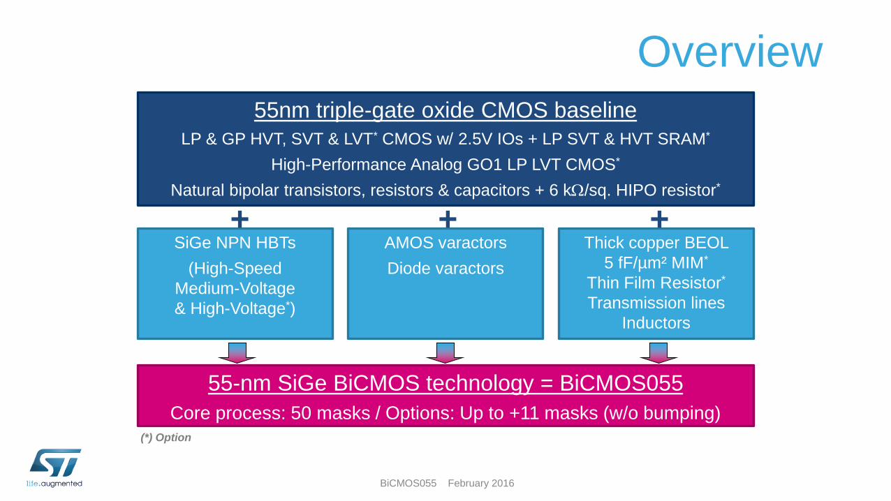
Overview
BiCMOS055 February 2016
55nm triple-gate oxide CMOS baseline
LP & GP HVT, SVT & LVT* CMOS w/ 2.5V IOs + LP SVT & HVT SRAM*
High-Performance Analog GO1 LP LVT CMOS*
Natural bipolar transistors, resistors & capacitors + 6 k/sq. HIPO resistor*
55-nm SiGe BiCMOS technology = BiCMOS055
Core process: 50 masks / Options: Up to +11 masks (w/o bumping)
SiGe NPN HBTs
(High-Speed
Medium-Voltage
& High-Voltage*)
AMOS varactors
Diode varactors
Thick copper BEOL
5 fF/µm² MIM*
Thin Film Resistor*
Transmission lines
Inductors
+ + +
(*) Option

Technology cross-sections
BiCMOS055 February 2016

BEOL schematic cross-section
• 9 metal layers (including Aluminum capping) BEOL obtained by the
introduction of a thick Via/Line copper module :• 3µm thick M8U and 1.5µm thick V7U
• MIM integrated in V5Z
• TFR integrated in V6Z
• All the 55-nm CMOS libraries
are therefore compatible
with BiCMOS055
BiCMOS055 February 2016
3.1µm
CMOS0557M4X2Z0U
polySi
M6Z
M5X
M1
Via4XVia5Z
M7Z
Via6Z
AP
polySi
M6Z
M5X
M1
Via4X
Via5Z
M7Z
Via6Z
5.5µm
M8U
AP
CB
Via7U
BiCMOS0558M4X2Z1U
MIM
TFR
M2 to Last Metal Layer

BiCMOS055 devices list (DK2.3)• Core
• LP/GP HVT & SVT CMOS w/ 2.5V GO2
(incl. RF SVT for LP, GP & GO2)
• High-Speed & Medium-Voltage SiGe HBTs
• Natural devices
• NPN & PNP bipolar transistors
• Resistors (active, poly & metal – incl. RF resistors)
• Diodes (N+/Pwell, P+/Nwell, Deep Nwell/Psub,…)
• DC capacitors (poly, plate)
• Varactors
• Single & Diff. GO1/GO2 P+ poly/Nwell varactors
• P+/Nwell diode varactor
• RF MOM
• MMW, HQ & LOHQ inductors
• µstrip transmission line
• Options• LP & GP CMOS LVT
(incl. RF models for LP & GP)
• SRAM SVT + HVT
• High-Performance Analog (HPA) CMOS
(incl. RF models)
• High-Voltage SiGe HBTs
• 6k/sq. HIPO resistor
(incl. RF model)
• 5fF/µm² MIM capacitor
(incl. RF model)
• Thin Film Resistor
• Flip-Chip bumping
BiCMOS055 February 2016

LP & GP CMOS
• Low Power (LP) and General Purpose (GP) CMOS
BiCMOS055 February 2016
Devices targets
DeviceLow Power MOS (TOX=18.5Å) General Purpose MOS (TOX=13Å)
ION (µA/µm) IOFF (nA/µm) ION (µA/µm) IOFF (nA/µm)
Low VT NMOS 740 5 970 382
Low VT PMOS 390 2.4 460 204
Standard VT NMOS 610 0.35 830 51
Standard VT PMOS 305 0.1 395 36
High VT NMOS 430 0.015 669 5
High VT PMOS 210 0.010 300 4
Ldrawn=0.06µm, Wdrawn= 1.0 µm, T=25°C

SiGe HBTs
• 3 collector flavors sharing the same E/B system
• Scalable emitter widths and lengths
BiCMOS055 February 2016
CBEBC: Wdrawn= 0.2 µm, Ldrawn=5.56µm, T=25°C
DevicefT
(GHz)
fMAX
(GHz)
BVCBO
(V)
BVCEO
(V)
HS NPN SiGe HBT
npnvhs, npnvhs_t
320
VCB=0.5V
VBE=0.90V
370
VCB=0.5V
VBE=0.90V
5.2
ICB=10µA
1.5
IB=0µA
MV NPN SiGe HBT
npnvmv, npnvmv_t
180
VCB=1.0V
VBE=0.87V
380
VCB=1.0V
VBE=0.87V
7.2
ICB=10µA
1.8
IB=0µA
HV NPN SiGe HBT
npnvhv, npnvhv_t
70
VCB=2.0V
VBE=0.80V
250
VCB=2.0V
VBE=0.80V
13.5
ICB=10µA
3.2
IB=0µA
Devices targets
E
Deep Trench Isolation (DTI)
B
As in-situ doped
EmitterB in-situ doped
SiGe:C Base
Shallow Trench Isolation (STI)
Localized Collector
Pedestal
oxide
Buried Layer
Epitaxial Collector
Collector Sinker
CB
B doped
Polybase
C CC C C
High-speed SiGe HBT schematic cross-section
Double Polysilicon Self-Aligned (DPSA) architecture
featuring a Selective Epitaxial Growth (SEG) of the base

Varactors & capacitors
• P+ Poly/NWell GO1 & GO2 benefit from short gate lengths
• RF MOM
• C0~0.9 fF/µm² (M1-M2) to ~3.0 fFµm² (M1-M5) / CV1 < 1 ppm/V
• MIM
• C0=5.0 fF/µm² / CV1 < 150 ppm/V / CV2 < 100 ppm/V²
BiCMOS055 February 2016
Device
Oxide
type
Capacitance
range
(Cmin / max)
Typical
tuning ratio
@ 25 GHz
@ C =100 fF
Max Q
@ C =100 fF
@ 25 GHz
@ V =1,2 V
Freq_res
@ C =100 fF
@ 1,2 V (GO1)
@ 2,5 V (GO2)
Varactor P+/NWell GO1 SE
cpo12nw_varGO1
1,2 V
5 fF / 1 pF 3
(max 5)
20 > 110 GHz
Varactor P+/NWell GO2 SE
cpo25nw_varGO2
2,5 V
5 fF / 1 pF 3
(max 5)
30 > 110 GHz
Devices targets

Inductors & transmission lines
• Inductors & TL benefit from the 8ML BEOL with thick V7/M8
BiCMOS055 February 2016
Devices targets
Device Stack L Qmax
Self
resonance
frequency
MMW Inductor
ind_mmw_8m4x0y2z1u
Coil M8U
Upath M7Z
Gnd ring M1
From 65pH
to 1.6nH
> 10 From 27GHz
to 300GHz
Device Stack Zc IL
µ-strip TL
microstrip_8m4x0y2z1u
Line in M8U
Gnd in M1 or M4
From 35
to 70
0.5dB/mm
@60GHz
4.25-turn inductor 3D view
1-turn inductor 3D view
M8 line
M1 gnd
Lateral wall
3D schematic view
Inductors geometry:
• Number of coil turns (n): 1 to 4.25
• Internal coil diameter (d): 10 to 50 µm
• Coil width (w): 0.6 to 4 µm

Masks count• All options are compatible with each other*
BiCMOS055 February 2016
Process options Masks count
Core process 50
SRAM 3
Triple-VT Low-VT (LVT, SVT and HVT transistors) 2
High-Performance Analog (HPA) CMOS 2/4*
HIPO (6k/sq poly resistor) 1
HV (High-Voltage) NPN 0
MIM (5fF/µm²) 2
TFR (Thin Film Resistor) 1
Flip-Chip 1(*) HPA CMOS are LVT MOS devices. This option requires 2 masks in addition
to LVT option, then 4 masks if standard LVT MOS devices are not used

Design kit & design platform
BiCMOS055 February 2016

Design kit
BiCMOS055 February 2016
Front-end/Schematic capture EDA tools EDA Vendors
Schematic Capture (Composer) IC Cadence
Simulation model libraries Eldo Mentor
Spectre Cadence
Hspice Synopsys
RF Simulation ADS (RFDE) Agilenteesof
GoldenGate Agilenteesof
ADS environment ADSKit ST
Layout Entry & Finishing EDA tools EDA Vendors
Layout Placement Virtuoso Layout Editor Cadence
Layout Verification : DRC/LVS
DFM YA/YE/YS
Calibre
pvs
Mentor
Cadence
Parasitic Extraction : interconnect RC StarRCXT
ext
Synopsys
Cadence
Post Layout Simulation flow PLSKit
Totem
ST
Apache

Design platform content
BiCMOS055 February 2016

Design platform flows
BiCMOS055 February 2016

Design platform version
BiCMOS055 February 2016
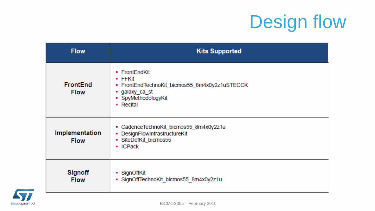
Design flow
BiCMOS055 February 2016