Embed Size (px)
Citation preview
Bharatiya Vidya Bhavan’s
Sardar Patel Institute of Technology (Autonomous Institute Affiliated to University of Mumbai)
Bachelor of Engineering/Technology (B.E./B.Tech)
in
Electronics Engineering
(Program Code: UEL)
Final Year Engineering (Sem. VII and Sem. VIII)
Effective from Academic Year 2018 -19
Board of Studies Approval: 13/12/2017
Academic Council Approval: 20/01/2018
Dr. Surendra Rathod Dr. Surendra Rathod Dr. Prachi Gharpure Head of Department Dean Academics Principal
Revision: SPIT-4-18
Sardar Patel Institute of Technology Bhavan‟s Campus, Munshi Nagar, Andheri (West), Mumbai-400058-India
(Autonomous Institute Affiliated to University of Mumbai)
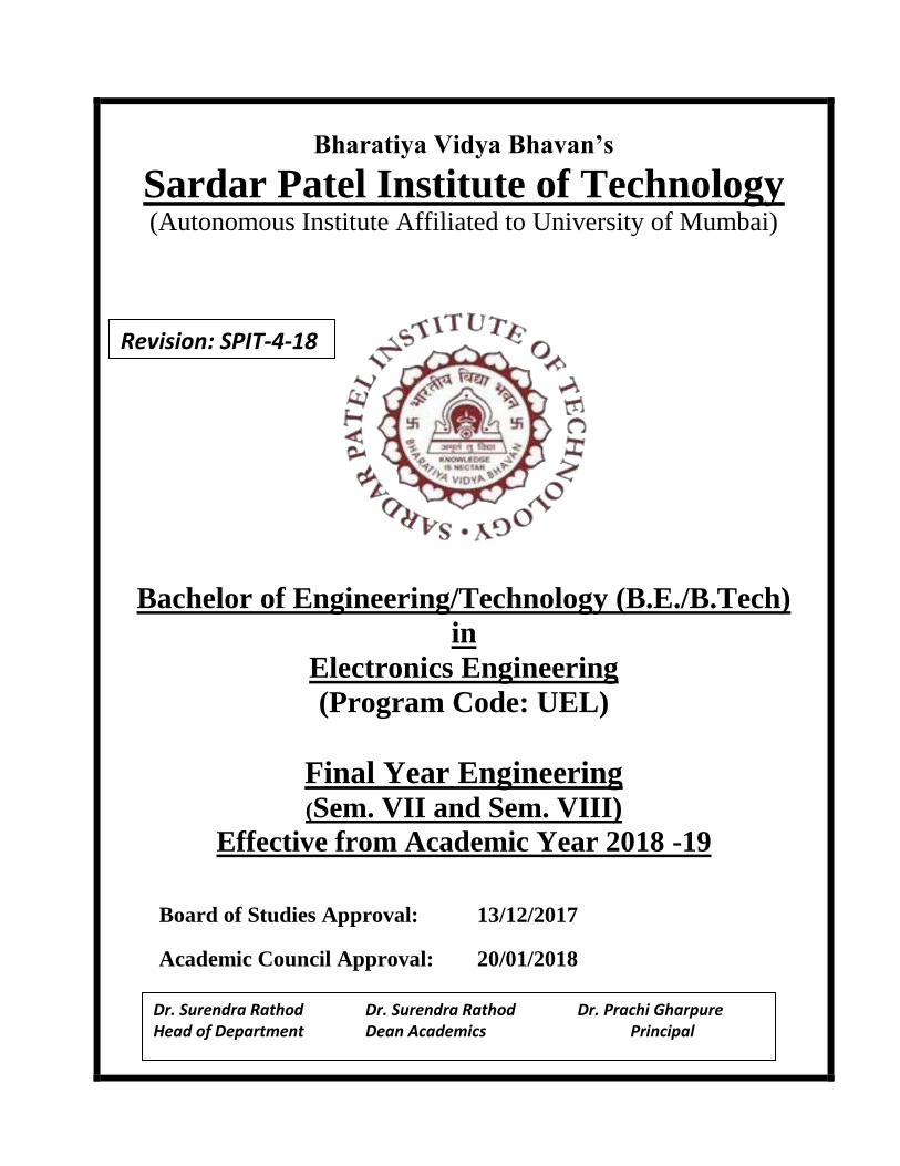
Scheme for B.E./B.Tech Electronics Engineering (SEM VII)
SEM VII
Course
Code
Course Name Teaching Scheme
(Hrs/week)
Credit
s
L T P Total
EXC701 Embedded System Design 4 -- -- 4
EXC702 IC Technology 4 -- -- 4
EXC703 Power Electronics –II 4 -- -- 4
EXC704 Computer Communication Networks 4 -- -- 4
EXC 705X Elective - I 4 -- -- 4
EXC 706 Project - I -- -- 4 2
EXL701 Embedded System Design
Laboratory
-- -- 2 1
EXL702 IC Technology Laboratory -- -- 2 1
EXL703 Power Electronics –II Laboratory -- -- 2 1
EXL704 Computer Communication Networks
Laboratory
-- -- 2 1
EXL 705X Elective - I Laboratory -- -- 2 1
Total 20 -- 14 27
Elective – I
Code Name of Elective
EXC7051 Digital Image Processing
EXC7052 Artificial Intelligence
EXC7053 ASIC Verification
EXC7054 Optical Fiber Communication
Sardar Patel Institute of Technology Bhavan‟s Campus, Munshi Nagar, Andheri (West), Mumbai-400058-India
(Autonomous Institute Affiliated to University of Mumbai)
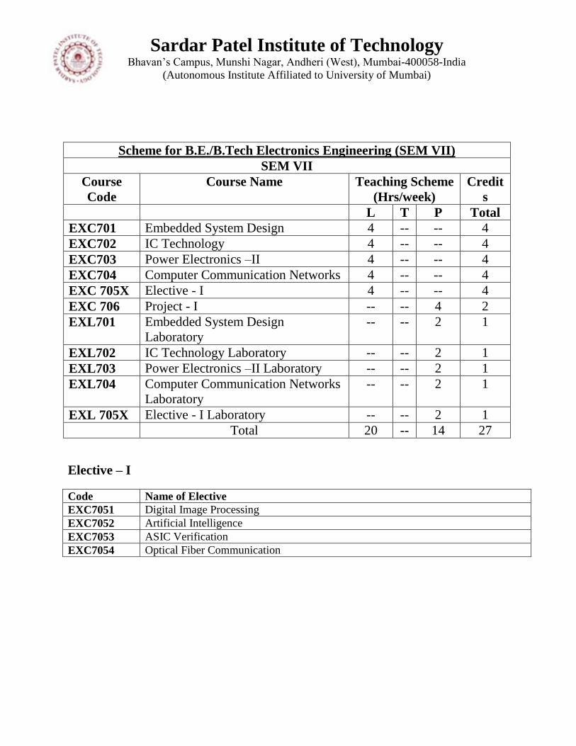
Scheme for B.Tech./B.Tech Electronics Engineering (SEM VIII)
SEM VIII
Course
Code
Course Name Teaching Scheme
(Hrs/week)
Credit
s
L T P Total EXC801 CMOS VLSI Design 4 -- -- 4 EXC802 Advanced Networking Technologies 4 -- -- 4 EXC803 MEMS Technology 4 -- -- 4 EXC804X Elective -II 4 -- -- 4 EXC806 Project (Stage II) -- -- 4 4 EXL801 CMOS VLSI Design Laboratory -- -- 2 1 EXL802 Advanced Networking Technologies
Laboratory -- -- 2 1
EXL803 MEMS Technology Laboratory -- -- 2 1 EXL804X Elective -II Laboratory -- -- 2 1
Total 16 -- 12 24
Elective – I
Code Name of Elective
EXC8041 Robotics
EXC8042 Mobile Communication
EXC8043 Digital Control System
EXC8044 Biomedical Electronics
Sardar Patel Institute of Technology Bhavan‟s Campus, Munshi Nagar, Andheri (West), Mumbai-400058-India
(Autonomous Institute Affiliated to University of Mumbai)
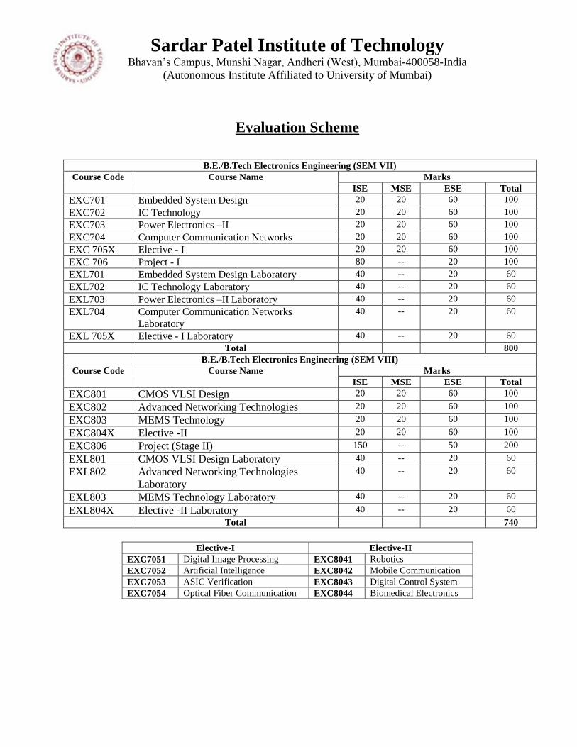
Evaluation Scheme
B.E./B.Tech Electronics Engineering (SEM VII)
Course Code Course Name Marks
ISE MSE ESE Total
EXC701 Embedded System Design 20 20 60 100
EXC702 IC Technology 20 20 60 100
EXC703 Power Electronics –II 20 20 60 100
EXC704 Computer Communication Networks 20 20 60 100
EXC 705X Elective - I 20 20 60 100
EXC 706 Project - I 80 -- 20 100
EXL701 Embedded System Design Laboratory 40 -- 20 60
EXL702 IC Technology Laboratory 40 -- 20 60
EXL703 Power Electronics –II Laboratory 40 -- 20 60
EXL704 Computer Communication Networks
Laboratory
40 -- 20 60
EXL 705X Elective - I Laboratory 40 -- 20 60
Total 800
B.E./B.Tech Electronics Engineering (SEM VIII)
Course Code Course Name Marks
ISE MSE ESE Total
EXC801 CMOS VLSI Design 20 20 60 100
EXC802 Advanced Networking Technologies 20 20 60 100
EXC803 MEMS Technology 20 20 60 100
EXC804X Elective -II 20 20 60 100
EXC806 Project (Stage II) 150 -- 50 200
EXL801 CMOS VLSI Design Laboratory 40 -- 20 60
EXL802 Advanced Networking Technologies
Laboratory
40 -- 20 60
EXL803 MEMS Technology Laboratory 40 -- 20 60
EXL804X Elective -II Laboratory 40 -- 20 60
Total 740
Elective-I Elective-II
EXC7051 Digital Image Processing EXC8041 Robotics
EXC7052 Artificial Intelligence EXC8042 Mobile Communication
EXC7053 ASIC Verification EXC8043 Digital Control System
EXC7054 Optical Fiber Communication EXC8044 Biomedical Electronics
Sardar Patel Institute of Technology Bhavan‟s Campus, Munshi Nagar, Andheri (West), Mumbai-400058-India
(Autonomous Institute Affiliated to University of Mumbai)
Semester VII
Sardar Patel Institute of Technology Bhavan‟s Campus, Munshi Nagar, Andheri (West), Mumbai-400058-India
(Autonomous Institute Affiliated to University of Mumbai)
Course
Code Course Name
Teaching
Scheme
(Hrs/week)
Credits Assigned
L T P L T P Total
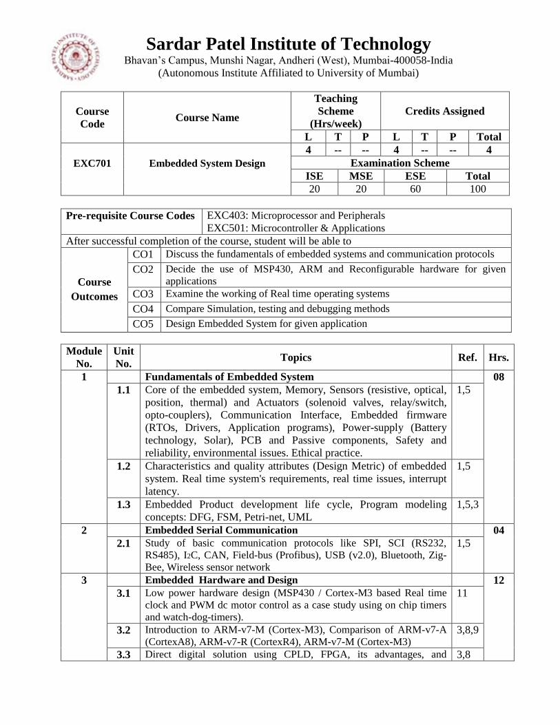
EXC701
Embedded System Design
4 -- -- 4 -- -- 4
Examination Scheme
ISE MSE ESE Total
20 20 60 100
Pre-requisite Course Codes EXC403: Microprocessor and Peripherals
EXC501: Microcontroller & Applications
After successful completion of the course, student will be able to
Course
Outcomes
CO1 Discuss the fundamentals of embedded systems and communication protocols
CO2 Decide the use of MSP430, ARM and Reconfigurable hardware for given
applications
CO3 Examine the working of Real time operating systems
CO4 Compare Simulation, testing and debugging methods
CO5 Design Embedded System for given application
Module
No.
Unit
No. Topics Ref. Hrs.
1 Fundamentals of Embedded System 08
1.1 Core of the embedded system, Memory, Sensors (resistive, optical,
position, thermal) and Actuators (solenoid valves, relay/switch,
opto-couplers), Communication Interface, Embedded firmware
(RTOs, Drivers, Application programs), Power-supply (Battery
technology, Solar), PCB and Passive components, Safety and
reliability, environmental issues. Ethical practice.
1,5
1.2 Characteristics and quality attributes (Design Metric) of embedded
system. Real time system's requirements, real time issues, interrupt
latency.
1,5
1.3 Embedded Product development life cycle, Program modeling
concepts: DFG, FSM, Petri-net, UML
1,5,3
2 Embedded Serial Communication 04
2.1 Study of basic communication protocols like SPI, SCI (RS232,
RS485), I2C, CAN, Field-bus (Profibus), USB (v2.0), Bluetooth, Zig-
Bee, Wireless sensor network
1,5
3 Embedded Hardware and Design 12
3.1 Low power hardware design (MSP430 / Cortex-M3 based Real time
clock and PWM dc motor control as a case study using on chip timers
and watch-dog-timers).
11
3.2 Introduction to ARM-v7-M (Cortex-M3), Comparison of ARM-v7-A
(CortexA8), ARM-v7-R (CortexR4), ARM-v7-M (Cortex-M3) 3,8,9
3.3 Direct digital solution using CPLD, FPGA, its advantages, and 3,8
Sardar Patel Institute of Technology Bhavan‟s Campus, Munshi Nagar, Andheri (West), Mumbai-400058-India
(Autonomous Institute Affiliated to University of Mumbai)
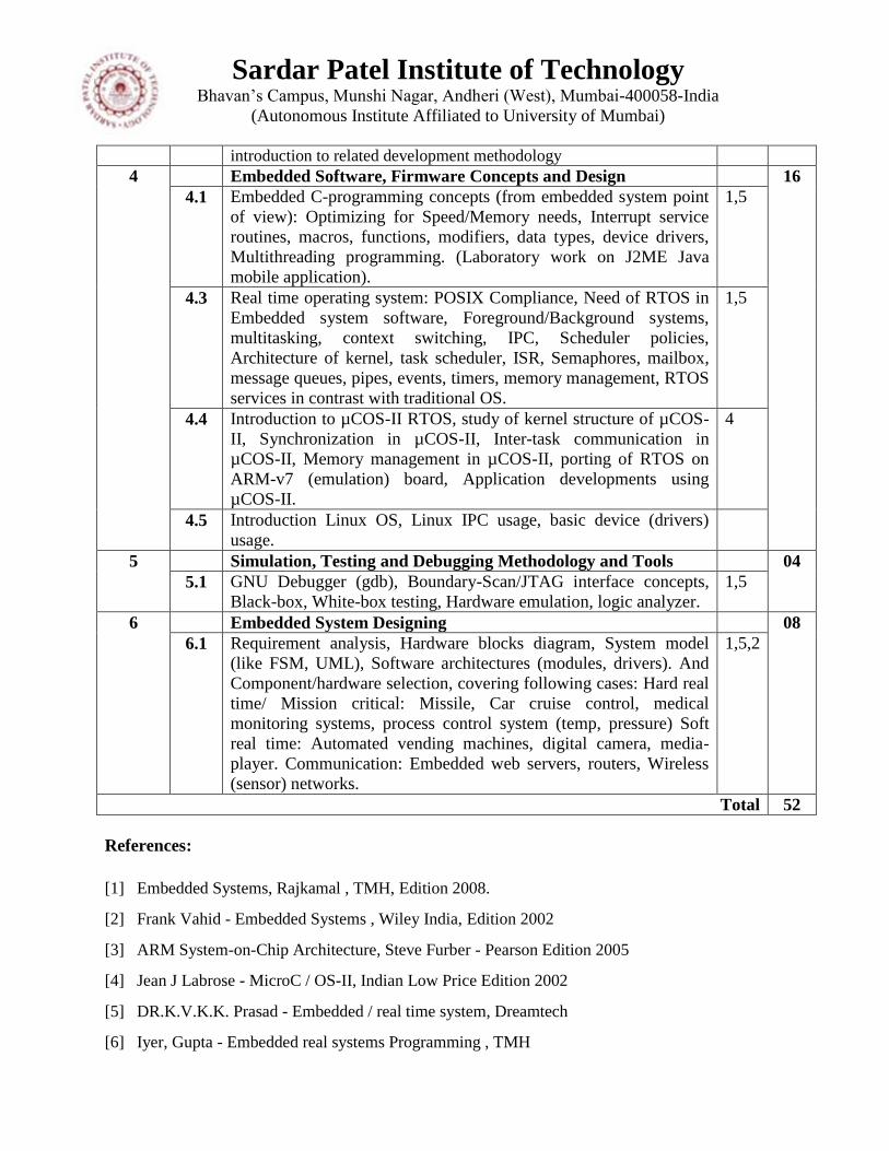
introduction to related development methodology
4 Embedded Software, Firmware Concepts and Design 16
4.1 Embedded C-programming concepts (from embedded system point
of view): Optimizing for Speed/Memory needs, Interrupt service
routines, macros, functions, modifiers, data types, device drivers,
Multithreading programming. (Laboratory work on J2ME Java
mobile application).
1,5
4.3 Real time operating system: POSIX Compliance, Need of RTOS in
Embedded system software, Foreground/Background systems,
multitasking, context switching, IPC, Scheduler policies,
Architecture of kernel, task scheduler, ISR, Semaphores, mailbox,
message queues, pipes, events, timers, memory management, RTOS
services in contrast with traditional OS.
1,5
4.4 Introduction to µCOS-II RTOS, study of kernel structure of µCOS-
II, Synchronization in µCOS-II, Inter-task communication in
µCOS-II, Memory management in µCOS-II, porting of RTOS on
ARM-v7 (emulation) board, Application developments using
µCOS-II.
4
4.5 Introduction Linux OS, Linux IPC usage, basic device (drivers)
usage.
5 Simulation, Testing and Debugging Methodology and Tools 04
5.1 GNU Debugger (gdb), Boundary-Scan/JTAG interface concepts,
Black-box, White-box testing, Hardware emulation, logic analyzer.
1,5
6 Embedded System Designing 08
6.1 Requirement analysis, Hardware blocks diagram, System model
(like FSM, UML), Software architectures (modules, drivers). And
Component/hardware selection, covering following cases: Hard real
time/ Mission critical: Missile, Car cruise control, medical
monitoring systems, process control system (temp, pressure) Soft
real time: Automated vending machines, digital camera, media-
player. Communication: Embedded web servers, routers, Wireless
(sensor) networks.
1,5,2
Total 52
References:
[1] Embedded Systems, Rajkamal , TMH, Edition 2008.
[2] Frank Vahid - Embedded Systems , Wiley India, Edition 2002
[3] ARM System-on-Chip Architecture, Steve Furber - Pearson Edition 2005
[4] Jean J Labrose - MicroC / OS-II, Indian Low Price Edition 2002
[5] DR.K.V.K.K. Prasad - Embedded / real time system, Dreamtech
[6] Iyer, Gupta - Embedded real systems Programming , TMH
Sardar Patel Institute of Technology Bhavan‟s Campus, Munshi Nagar, Andheri (West), Mumbai-400058-India
(Autonomous Institute Affiliated to University of Mumbai) [7] Embedded systems software primer, David Simon - Pearson
[8] ARM System Developers Guide- Sloss, Symes, Wright, ElsevierMorgan Kaufman, Edition 2005
[9] LPC2148 Data Sheets www.arm.com
[10] ARM Programers/architectural manual.
[11] MSP430 architectural manual.
[12] Embedded Microcomputer Systems – Real Time Interfacing – Jonathan W. Valvano; Cengage
Learning; Third or later edition.
Sardar Patel Institute of Technology Bhavan‟s Campus, Munshi Nagar, Andheri (West), Mumbai-400058-India
(Autonomous Institute Affiliated to University of Mumbai)
Course
Code Course Name
Teaching
Scheme
(Hrs/week)
Credits Assigned
L T P L T P Total
EXC702
IC Technology
4 -- -- 4 -- -- 4
Examination Scheme
ISE MSE ESE Total
20 20 60 100
Pre-requisite Course Codes EXC302: Electronic Devices
EXC303: Digital Circuits and Design
EXC402: Discrete Electronic Circuits
EXC502: Design With Linear Integrated Circuits
EXC601: VLSI Design
At the end of successful completion of the course, student will be able to
Course
Outcomes
CO1 Discuss integrated circuit fabrication processes
CO2 Illustrate the sequence of process of semiconductor device fabrication
CO3 Discuss the semiconductor parameter measurement techniques
CO4 Interpret the physical mechanism of novel semiconductor devices
CO5 Summarize features of novel semiconductor devices and justify use of these
devices in an application
Module
No.
Unit
No. Topics Ref. Hrs.
1 Environment and Crystal Growth for VLSI Technology 08
1.1 Environment: Semiconductor technology trend, Clean rooms, Wafer
cleaning 1,2,3,4
1.2 Semiconductor Substrate: Phase diagram and solid solubility,
Crystal structure, Crystal defects, Czochralski growth, Bridgman
growth of GaAs, Float Zone growth, Wafer Preparation and
specifications
1,2,3,4
2 Fabrication Processes Part 1 10
2.1 Deposition: Evaporation, Sputtering and Chemical Vapor Deposition 1,2,3,4
2.2 Epitaxy: Molecular Beam Epitaxy, Vapor Phase Epitaxy, Liquid
Phase Epitaxy, Evaluation of epitaxial layers 1,2,3,4
2.3 Silicon Oxidation: Thermal oxidation process, Kinetics of growth,
Properties of Silicon Dioxide, Oxide Quality, high κ and low κ
dielectrics
1,2,3,4
2.4 Diffusion: Nature of diffusion, Diffusion in a concentration gradient,
diffusion equation, impurity behavior, diffusion systems, problems in
diffusion, evaluation of diffused layers
1,2,3,4
2.5 Ion Implantation: Penetration range, ion implantation systems,
process considerations, implantation damage and annealing 1,2,3,4
3 Fabrication Processess Part 2 10
3.1 Etching: Wet chemical etching, dry physical etching, dry chemical 1,2,3,4

Sardar Patel Institute of Technology Bhavan‟s Campus, Munshi Nagar, Andheri (West), Mumbai-400058-India
(Autonomous Institute Affiliated to University of Mumbai)
etching, reactive ion etching, ion beam techniques
3.2 Lithography: Photoreactive materials, Pattern generation and mask
making, pattern transfer, Electron beam, Ion beam and X-ray
lithography
1,2,3,4
3.3 Device Isolation, Contacts and Metallization: Junction and oxide
isolation, LOCOS, trench isolation, Schottky contacts, Ohmic
contacts, Metallization and Packaging
1,2,3,4
3.4 CMOS Process Flow: N well, P-well and Twin tub 1,2,3,4
3.5 Design rules, Layout of MOS based circuits (gates and combinational
logic), Buried and Butting Contact 1,2,3,4
4 Measurements, Packaging and Testing 10
4.1 Semiconductor Measurements: Conductivity type, Resistivity, Hall
Effect Measurements, Drift Mobility, Minority Carrier Lifetime and
diffusion length
7
4.2 Packaging: Integrated circuit packages, Electronics package
reliability 9
4.3 Testing: Technology trends affecting testing, VLSI testing process
and test equipment, test economics and product quality 10
5 SOI, GaAs and Bipolar Technologies 8
5.1 SOI Technology: SOI fabrication using SIMOX, Bonded SOI and
Smart Cut, PD SOI and FD SOI Device structure and their features 5
5.2 GaAs Technologies: MESFET Technology, Digital Technologies,
MMIC technologies, MODFET and Optoelectronic Devices 8
5.3 Silicon Bipolar Technologies: Second order effects in bipolar
transistor, Performance of BJT, Bipolar processes and BiCMOS 8
6 Novel Devices 6
6.1 Multigate Device: Various multigate device configurations (device
structure and important features) 6
6.2 Nanowire: Fabrication and applications 8
6.3 Graphene Device: Carbon nanotube transistor fabrication, CNT
applications 8
Total 52
References:
[1] James D. Plummer, Michael D. Deal and Peter B. Griffin, “Silicon VLSI Technology”, Pearson,
Indian Edition.
[2] Stephen A. Campbell, “The Science and Engineering of Microelectronic Fabrication”, Oxford
University Press, Second Edition.
[3] Sorab K. Gandhi, “VLSI Fabrication Principles”, Wiley, Student Edition.
[4] G. S. May and S. M. Sze, “Fundamentals of Semiconductor Fabrication”, Wiley, First Edition.
Sardar Patel Institute of Technology Bhavan‟s Campus, Munshi Nagar, Andheri (West), Mumbai-400058-India
(Autonomous Institute Affiliated to University of Mumbai)
[5] Kerry Bernstein and N. J. Rohrer, “SOI Circuit Design Concepts”, Kluwer Academic Publishers,
First edition.
[6] Jean-Pierre Colinge, “FinFETs and Other Multigate Transistors”, Springer, First edition
[7] M. S. Tyagi, “Introduction to Semiconductor Materials and Devices”, John Wiley and Sons, First
Edition.
[8] James E. Morris and Krzysztol Iniewski, “Nanoelectronic Device Applications Handbook”, CRC
Press
[9] Glenn R. Blackwell, “The electronic packaging”, CRC Press
[10] Michael L. Bushnell and Vishwani D. Agrawal, “Essentials of Electronic Testing for digital,
memory and mixed-signal VLSI circuits”, Springer
Sardar Patel Institute of Technology Bhavan‟s Campus, Munshi Nagar, Andheri (West), Mumbai-400058-India
(Autonomous Institute Affiliated to University of Mumbai)
Course
Code Course Name
Teaching
Scheme
(Hrs/week)
Credits Assigned
L T P L T P Total
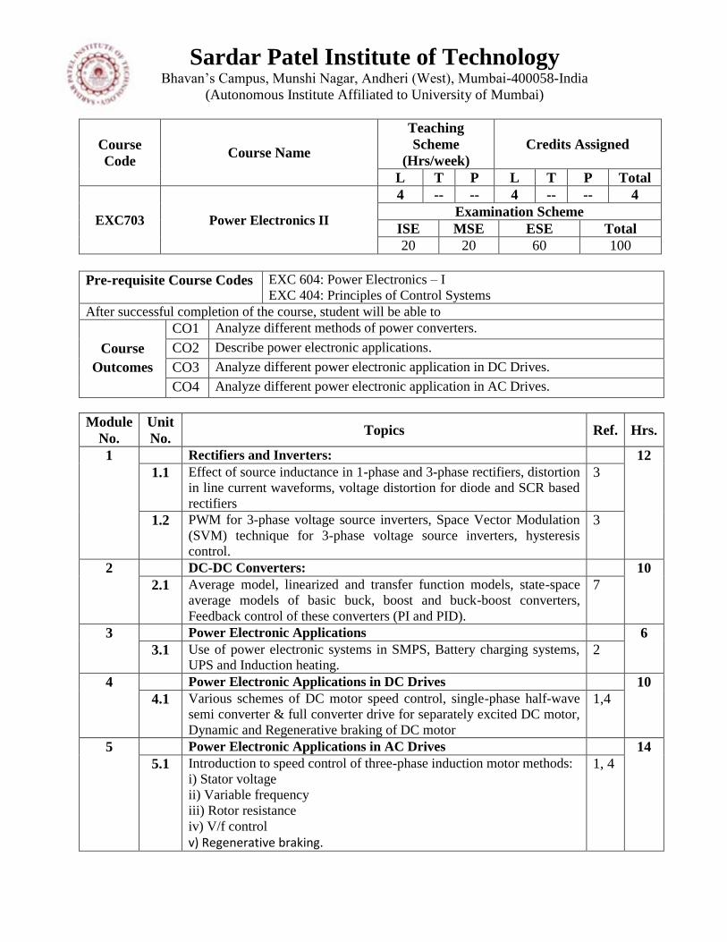
EXC703 Power Electronics II
4 -- -- 4 -- -- 4
Examination Scheme
ISE MSE ESE Total
20 20 60 100
Pre-requisite Course Codes EXC 604: Power Electronics – I
EXC 404: Principles of Control Systems
After successful completion of the course, student will be able to
Course
Outcomes
CO1 Analyze different methods of power converters.
CO2 Describe power electronic applications.
CO3 Analyze different power electronic application in DC Drives.
CO4 Analyze different power electronic application in AC Drives.
Module
No.
Unit
No. Topics Ref. Hrs.
1 Rectifiers and Inverters: 12
1.1 Effect of source inductance in 1-phase and 3-phase rectifiers, distortion
in line current waveforms, voltage distortion for diode and SCR based
rectifiers
3
1.2 PWM for 3-phase voltage source inverters, Space Vector Modulation
(SVM) technique for 3-phase voltage source inverters, hysteresis
control.
3
2 DC-DC Converters: 10
2.1 Average model, linearized and transfer function models, state-space
average models of basic buck, boost and buck-boost converters,
Feedback control of these converters (PI and PID).
7
3 Power Electronic Applications 6
3.1 Use of power electronic systems in SMPS, Battery charging systems,
UPS and Induction heating. 2
4 Power Electronic Applications in DC Drives 10
4.1 Various schemes of DC motor speed control, single-phase half-wave
semi converter & full converter drive for separately excited DC motor,
Dynamic and Regenerative braking of DC motor
1,4
5 Power Electronic Applications in AC Drives 14
5.1 Introduction to speed control of three-phase induction motor methods:
i) Stator voltage
ii) Variable frequency
iii) Rotor resistance
iv) V/f control
v) Regenerative braking.
1, 4
Sardar Patel Institute of Technology Bhavan‟s Campus, Munshi Nagar, Andheri (West), Mumbai-400058-India
(Autonomous Institute Affiliated to University of Mumbai)
Total 52
References:
[1] M. Rashid, Power Electronics: Circuits, Devices, and Applications, PHI, Third Edition.
[2]. By M. D. Singh, K. B. Khanchandani, Power Electronics, Tata McGraw Hill, Second Edition.
[3]. Mohan, Undeland and Riobbins, Power Electronics: Converters, Applications and Design, Wiley
(Student Edition), Second Edition.
[4]. P. S. Bimbhra, Power Electronics, Khanna Publishers, Edition 2012.
[5]. R. W. Erickson, D. Maksimovic, Fundamentals of Power Electronics, Springer, Second Edition.
[6]. J. P. Agrawal, Power Electronics Systems: Theory and Design, Pearson Education, Edition
2002.
[7]. S. Bacha, I. Munteanu and A. Bratcu, Power Electronic Converters: Modeling and Control,
Springer-Verlag, Edition 2014.
[8]. H. Sira-Ramírez, R. Silva-Ortigoza, Control Design Techniques in Power Electronics Devices,
Springer-Verlag, Edition 2006
Sardar Patel Institute of Technology Bhavan‟s Campus, Munshi Nagar, Andheri (West), Mumbai-400058-India
(Autonomous Institute Affiliated to University of Mumbai)
Course
Code Course Name
Teaching
Scheme
(Hrs/week)
Credits Assigned
L T P L T P Total
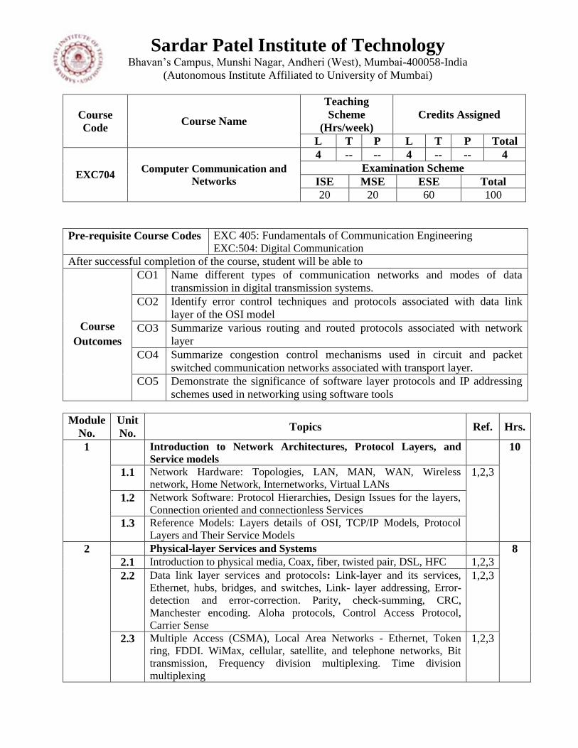
EXC704
Computer Communication and
Networks
4 -- -- 4 -- -- 4
Examination Scheme
ISE MSE ESE Total
20 20 60 100
Pre-requisite Course Codes EXC 405: Fundamentals of Communication Engineering EXC:504: Digital Communication
After successful completion of the course, student will be able to
Course
Outcomes
CO1 Name different types of communication networks and modes of data
transmission in digital transmission systems.
CO2 Identify error control techniques and protocols associated with data link
layer of the OSI model
CO3 Summarize various routing and routed protocols associated with network
layer
CO4 Summarize congestion control mechanisms used in circuit and packet
switched communication networks associated with transport layer.
CO5 Demonstrate the significance of software layer protocols and IP addressing
schemes used in networking using software tools
Module
No.
Unit
No. Topics Ref. Hrs.
1 Introduction to Network Architectures, Protocol Layers, and
Service models 10
1.1 Network Hardware: Topologies, LAN, MAN, WAN, Wireless
network, Home Network, Internetworks, Virtual LANs 1,2,3
1.2 Network Software: Protocol Hierarchies, Design Issues for the layers,
Connection oriented and connectionless Services
1.3 Reference Models: Layers details of OSI, TCP/IP Models, Protocol
Layers and Their Service Models
2 Physical-layer Services and Systems 8
2.1 Introduction to physical media, Coax, fiber, twisted pair, DSL, HFC 1,2,3
2.2 Data link layer services and protocols: Link-layer and its services,
Ethernet, hubs, bridges, and switches, Link- layer addressing, Error-
detection and error-correction. Parity, check-summing, CRC,
Manchester encoding. Aloha protocols, Control Access Protocol,
Carrier Sense
1,2,3
2.3 Multiple Access (CSMA), Local Area Networks - Ethernet, Token
ring, FDDI. WiMax, cellular, satellite, and telephone networks, Bit
transmission, Frequency division multiplexing. Time division
multiplexing
1,2,3
Sardar Patel Institute of Technology Bhavan‟s Campus, Munshi Nagar, Andheri (West), Mumbai-400058-India
(Autonomous Institute Affiliated to University of Mumbai)
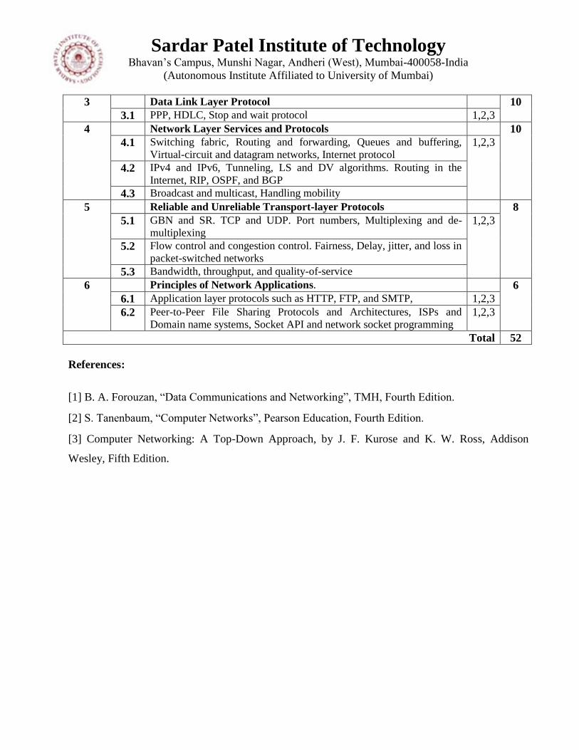
3 Data Link Layer Protocol 10
3.1 PPP, HDLC, Stop and wait protocol 1,2,3
4 Network Layer Services and Protocols 10
4.1 Switching fabric, Routing and forwarding, Queues and buffering,
Virtual-circuit and datagram networks, Internet protocol 1,2,3
4.2 IPv4 and IPv6, Tunneling, LS and DV algorithms. Routing in the
Internet, RIP, OSPF, and BGP
4.3 Broadcast and multicast, Handling mobility
5 Reliable and Unreliable Transport-layer Protocols 8
5.1 GBN and SR. TCP and UDP. Port numbers, Multiplexing and de-
multiplexing 1,2,3
5.2 Flow control and congestion control. Fairness, Delay, jitter, and loss in
packet-switched networks
5.3 Bandwidth, throughput, and quality-of-service
6 Principles of Network Applications. 6
6.1 Application layer protocols such as HTTP, FTP, and SMTP, 1,2,3
6.2 Peer-to-Peer File Sharing Protocols and Architectures, ISPs and
Domain name systems, Socket API and network socket programming 1,2,3
Total 52
References:
[1] B. A. Forouzan, “Data Communications and Networking”, TMH, Fourth Edition.
[2] S. Tanenbaum, “Computer Networks”, Pearson Education, Fourth Edition.
[3] Computer Networking: A Top-Down Approach, by J. F. Kurose and K. W. Ross, Addison
Wesley, Fifth Edition.
Sardar Patel Institute of Technology Bhavan‟s Campus, Munshi Nagar, Andheri (West), Mumbai-400058-India
(Autonomous Institute Affiliated to University of Mumbai)
Course
Code Course Name
Teaching
Scheme
(Hrs/week)
Credits Assigned
L T P L T P Total
EXC7051
Digital Image Processing
4 -- -- 4 -- -- 4
Examination Scheme
ISE MSE ESE Total
20 20 60 100
Pre-requisite Course Codes EXS 401 : Applied Mathematics IV EXC 504 : Signal and Systems
After successful completion of the course, student will be able to
Course
Outcomes
CO1 Discuss the fundamental concepts of digital image processing
CO2 Discuss image enhancement and segmentation techniques
CO3 Apply suitable operators for binary image processing
CO4 Apply suitable transform techniques on digital image
CO5 Discuss digital image compression and decompression techniques
Module
No.
Unit
No. Topics Ref. Hrs.
1 Digital Image Processing Fundamentals 06
1.1 Introduction: Background, Digital Image Representation,
Fundamental Steps in Image Processing, Elements of a Digital Image
Processing System
1,2,3
1.2 Digital Image Fundamentals: Elements of Visual Perception, A
Simple Image Model, Sampling and Quantization, Some Basic
Relationships between Pixels, Imagining Geometry. Image File
Formats : BMP, TIFF and JPEG. Colour Models
(RGB, HSI, YUV)
1,2,3
2 Image Enhancement 08
2.1 Spatial Domain Methods, Frequency Domain Methods, Some Simple
Intensity Transformations, Histogram Processing, Image Subtraction,
Image Averaging, Background
1,2,3
2.2 Smoothing Filters, Sharpening Filters, Lowpass Filtering, Highpass
Filtering, Generation of Spatial Masks from Frequency Domain
Specifications. Homomorphic Filtering.
1,2,3
3 Image Segmentation and Representation 08
3.1 Detection of Discontinuities, Edge Linking using Hough Transform,
Thresholding, Region based Segmentation, Split and Merge Technique 1,2,3
3.2 Image Representation and Description, Chain Code, Polygonal,
Representation, Shape Number, Moments. 1,2,3
4 Binary Image Processing 06
4.1 Binary Morphological Operators, Hit-or-Miss Transformation,
Boundary Extraction, Region Filling, Thinning and Thickening, 1,2,3
Sardar Patel Institute of Technology Bhavan‟s Campus, Munshi Nagar, Andheri (West), Mumbai-400058-India
(Autonomous Institute Affiliated to University of Mumbai)
Connected Component Labeling, Iterative Algorithm and Classical
Algorithm
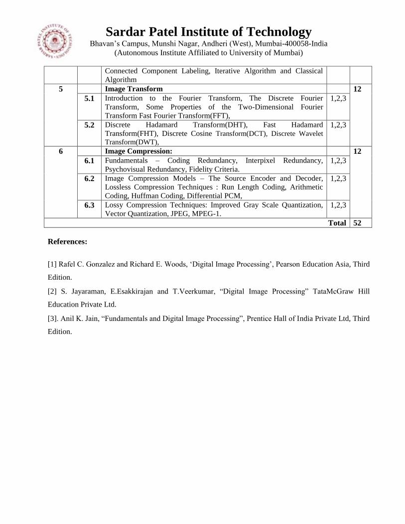
5 Image Transform 12
5.1 Introduction to the Fourier Transform, The Discrete Fourier
Transform, Some Properties of the Two-Dimensional Fourier
Transform Fast Fourier Transform(FFT),
1,2,3
5.2 Discrete Hadamard Transform(DHT), Fast Hadamard
Transform(FHT), Discrete Cosine Transform(DCT), Discrete Wavelet
Transform(DWT),
1,2,3
6 Image Compression: 12
6.1 Fundamentals – Coding Redundancy, Interpixel Redundancy,
Psychovisual Redundancy, Fidelity Criteria. 1,2,3
6.2 Image Compression Models – The Source Encoder and Decoder,
Lossless Compression Techniques : Run Length Coding, Arithmetic
Coding, Huffman Coding, Differential PCM,
1,2,3
6.3 Lossy Compression Techniques: Improved Gray Scale Quantization,
Vector Quantization, JPEG, MPEG-1. 1,2,3
Total 52
References:
[1] Rafel C. Gonzalez and Richard E. Woods, „Digital Image Processing‟, Pearson Education Asia, Third
Edition.
[2] S. Jayaraman, E.Esakkirajan and T.Veerkumar, “Digital Image Processing” TataMcGraw Hill
Education Private Ltd.
[3]. Anil K. Jain, “Fundamentals and Digital Image Processing”, Prentice Hall of India Private Ltd, Third
Edition.
Sardar Patel Institute of Technology Bhavan‟s Campus, Munshi Nagar, Andheri (West), Mumbai-400058-India
(Autonomous Institute Affiliated to University of Mumbai)
Course
Code Course Name
Teaching
Scheme
(Hrs/week)
Credits Assigned
L T P L T P Total
EXC7052
Artificial Intelligence
4 -- -- 4 -- -- 4
Examination Scheme
ISE MSE ESE Total
20 20 60 100
Pre-requisite Course Codes Knowledge of linear algebra, multivariate calculus, and probability
theory Knowledge of a programming language (MATLAB /C/C ++
recommended)
After successful completion of the course, student will be able to
Course
Outcomes
CO1 Classify different types of neural networks
CO2 Identify type of neural network algorithm for given application
CO3 Design a neural network for a given application
CO4 Apply different fuzzy operations to design fuzzy controller
Module
No.
Unit
No. Topics Ref. Hrs.
1 Fundamental Concepts of Neural Networks 08
1.1 Difference between fuzzy and crisp sets and applications of fuzzy logic 4
1.2 Biological neurons, McCulloch and Pitts models of neuron, Important
Terms of ANNs, McCulloch-Pitts Neuron, Hebb Network, Supervised
learning
3,2
1.3 Applications and scope of Neural Network 3
2 Supervised Learning Networks 12
2.1 Perception Networks: Adaline, Madaline 3,2
2.2 Back Propagation Network 3
2.3 Function Network 3
3 Unsupervised learning network 12
3.1 Max Net, Mexican Hat, Kohonen Self-organizing Feature 3
3.2 Maps, Learning Vector Quantization, Adaptive Resonance Theory 3
4 Associative networks 10
4.1 Pattern Association, Auto-associative Memory Network, Hetero-
associative Memory Network, Bidirectional Associative Memory,
Discrete Hopfield Networks
3
4.2 Special networks:
Simulated annealing neural networks, Boltzmann machine, Brain-in-a-Box
3
5 Fuzzy Logic 10
5.1 Fuzzy sets, Properties, Operations on fuzzy sets, Fuzzy relation
Operations on fuzzy relations, 4,3
Sardar Patel Institute of Technology Bhavan‟s Campus, Munshi Nagar, Andheri (West), Mumbai-400058-India
(Autonomous Institute Affiliated to University of Mumbai)
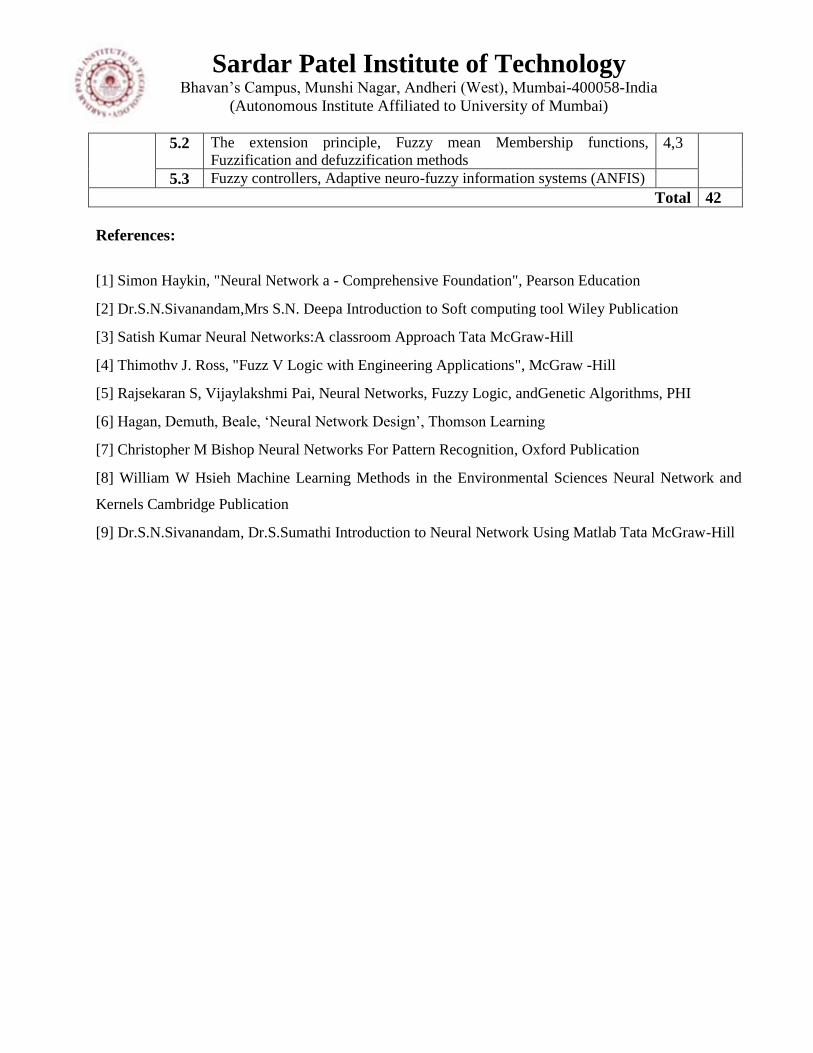
5.2 The extension principle, Fuzzy mean Membership functions,
Fuzzification and defuzzification methods 4,3
5.3 Fuzzy controllers, Adaptive neuro-fuzzy information systems (ANFIS)
Total 42
References:
[1] Simon Haykin, "Neural Network a - Comprehensive Foundation", Pearson Education
[2] Dr.S.N.Sivanandam,Mrs S.N. Deepa Introduction to Soft computing tool Wiley Publication
[3] Satish Kumar Neural Networks:A classroom Approach Tata McGraw-Hill
[4] Thimothv J. Ross, "Fuzz V Logic with Engineering Applications", McGraw -Hill
[5] Rajsekaran S, Vijaylakshmi Pai, Neural Networks, Fuzzy Logic, andGenetic Algorithms, PHI
[6] Hagan, Demuth, Beale, „Neural Network Design‟, Thomson Learning
[7] Christopher M Bishop Neural Networks For Pattern Recognition, Oxford Publication
[8] William W Hsieh Machine Learning Methods in the Environmental Sciences Neural Network and
Kernels Cambridge Publication
[9] Dr.S.N.Sivanandam, Dr.S.Sumathi Introduction to Neural Network Using Matlab Tata McGraw-Hill
Sardar Patel Institute of Technology Bhavan‟s Campus, Munshi Nagar, Andheri (West), Mumbai-400058-India
(Autonomous Institute Affiliated to University of Mumbai)
Course
Code Course Name
Teaching
Scheme
(Hrs/week)
Credits Assigned
L T P L T P Total
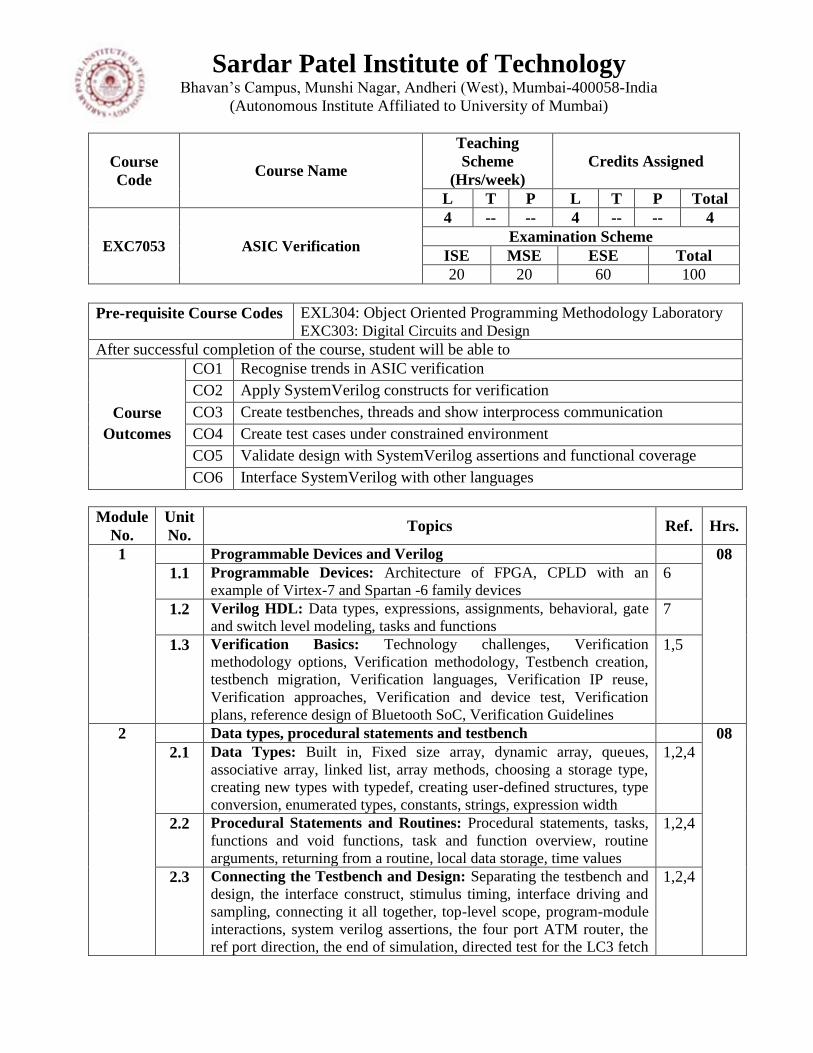
EXC7053 ASIC Verification
4 -- -- 4 -- -- 4
Examination Scheme
ISE MSE ESE Total
20 20 60 100
Pre-requisite Course Codes EXL304: Object Oriented Programming Methodology Laboratory EXC303: Digital Circuits and Design
After successful completion of the course, student will be able to
Course
Outcomes
CO1 Recognise trends in ASIC verification
CO2 Apply SystemVerilog constructs for verification
CO3 Create testbenches, threads and show interprocess communication
CO4 Create test cases under constrained environment
CO5 Validate design with SystemVerilog assertions and functional coverage
CO6 Interface SystemVerilog with other languages
Module
No.
Unit
No. Topics Ref. Hrs.
1 Programmable Devices and Verilog 08
1.1 Programmable Devices: Architecture of FPGA, CPLD with an
example of Virtex-7 and Spartan -6 family devices 6
1.2 Verilog HDL: Data types, expressions, assignments, behavioral, gate
and switch level modeling, tasks and functions 7
1.3 Verification Basics: Technology challenges, Verification
methodology options, Verification methodology, Testbench creation,
testbench migration, Verification languages, Verification IP reuse,
Verification approaches, Verification and device test, Verification
plans, reference design of Bluetooth SoC, Verification Guidelines
1,5
2 Data types, procedural statements and testbench 08
2.1 Data Types: Built in, Fixed size array, dynamic array, queues,
associative array, linked list, array methods, choosing a storage type,
creating new types with typedef, creating user-defined structures, type
conversion, enumerated types, constants, strings, expression width
1,2,4
2.2 Procedural Statements and Routines: Procedural statements, tasks,
functions and void functions, task and function overview, routine
arguments, returning from a routine, local data storage, time values
1,2,4
2.3 Connecting the Testbench and Design: Separating the testbench and
design, the interface construct, stimulus timing, interface driving and
sampling, connecting it all together, top-level scope, program-module
interactions, system verilog assertions, the four port ATM router, the
ref port direction, the end of simulation, directed test for the LC3 fetch
1,2,4
Sardar Patel Institute of Technology Bhavan‟s Campus, Munshi Nagar, Andheri (West), Mumbai-400058-India
(Autonomous Institute Affiliated to University of Mumbai)
block
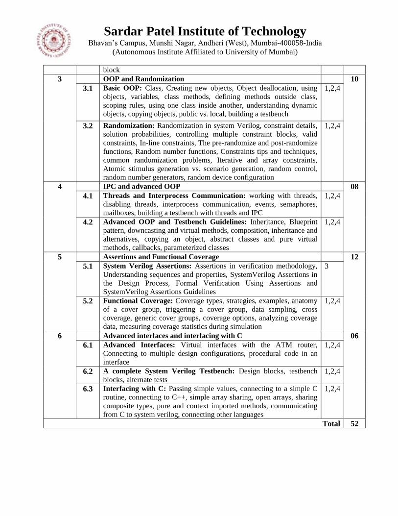
3 OOP and Randomization 10
3.1 Basic OOP: Class, Creating new objects, Object deallocation, using
objects, variables, class methods, defining methods outside class,
scoping rules, using one class inside another, understanding dynamic
objects, copying objects, public vs. local, building a testbench
1,2,4
3.2 Randomization: Randomization in system Verilog, constraint details,
solution probabilities, controlling multiple constraint blocks, valid
constraints, In-line constraints, The pre-randomize and post-randomize
functions, Random number functions, Constraints tips and techniques,
common randomization problems, Iterative and array constraints,
Atomic stimulus generation vs. scenario generation, random control,
random number generators, random device configuration
1,2,4
4 IPC and advanced OOP 08
4.1 Threads and Interprocess Communication: working with threads,
disabling threads, interprocess communication, events, semaphores,
mailboxes, building a testbench with threads and IPC
1,2,4
4.2 Advanced OOP and Testbench Guidelines: Inheritance, Blueprint
pattern, downcasting and virtual methods, composition, inheritance and
alternatives, copying an object, abstract classes and pure virtual
methods, callbacks, parameterized classes
1,2,4
5 Assertions and Functional Coverage 12
5.1 System Verilog Assertions: Assertions in verification methodology,
Understanding sequences and properties, SystemVerilog Assertions in
the Design Process, Formal Verification Using Assertions and
SystemVerilog Assertions Guidelines
3
5.2 Functional Coverage: Coverage types, strategies, examples, anatomy
of a cover group, triggering a cover group, data sampling, cross
coverage, generic cover groups, coverage options, analyzing coverage
data, measuring coverage statistics during simulation
1,2,4
6 Advanced interfaces and interfacing with C 06
6.1 Advanced Interfaces: Virtual interfaces with the ATM router,
Connecting to multiple design configurations, procedural code in an
interface
1,2,4
6.2 A complete System Verilog Testbench: Design blocks, testbench
blocks, alternate tests 1,2,4
6.3 Interfacing with C: Passing simple values, connecting to a simple C
routine, connecting to C++, simple array sharing, open arrays, sharing
composite types, pure and context imported methods, communicating
from C to system verilog, connecting other languages
1,2,4
Total 52
Sardar Patel Institute of Technology Bhavan‟s Campus, Munshi Nagar, Andheri (West), Mumbai-400058-India
(Autonomous Institute Affiliated to University of Mumbai)
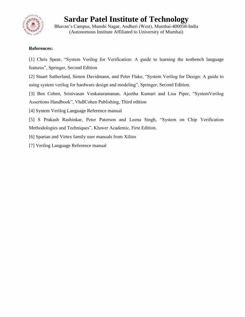
References:
[1] Chris Spear, “System Verilog for Verification: A guide to learning the testbench language
features”, Springer, Second Edition
[2] Stuart Sutherland, Simon Davidmann, and Peter Flake, “System Verilog for Design: A guide to
using system verilog for hardware design and modeling”, Springer, Second Edition.
[3] Ben Cohen, Srinivasan Venkataramanan, Ajeetha Kumari and Lisa Piper, “SystemVerilog
Assertions Handbook”, VhdlCohen Publishing, Third edition
[4] System Verilog Language Reference manual
[5] S Prakash Rashinkar, Peter Paterson and Leena Singh, “System on Chip Verification
Methodologies and Techniques”, Kluwer Academic, First Edition.
[6] Spartan and Virtex family user manuals from Xilinx
[7] Verilog Language Reference manual
Sardar Patel Institute of Technology Bhavan‟s Campus, Munshi Nagar, Andheri (West), Mumbai-400058-India
(Autonomous Institute Affiliated to University of Mumbai)
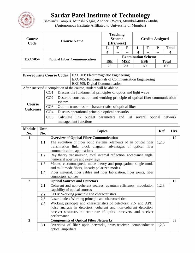
Course
Code Course Name
Teaching
Scheme
(Hrs/week)
Credits Assigned
L T P L T P Total
EXC7054 Optical Fiber Communication
4 -- -- 4 -- -- 4
Examination Scheme
ISE MSE ESE Total
20 20 60 100
Pre-requisite Course Codes EXC503: Electromagnetic Engineering
EXC405: Fundamentals of Communication Engineering
EXC505: Digital Communication.
After successful completion of the course, student will be able to
Course
Outcomes
CO1 Discuss the fundamental principles of optics and light wave
CO2 Describe construction and working principle of optical fiber communication
system
CO3 Outline transmission characteristics of optical fiber
CO4 Discuss operational principle optical networks
CO5 Calculate link budget parameters and list several optical network
management functions
Module
No.
Unit
No. Topics Ref. Hrs.
1 Overview of Optical Fiber Communication 10
1.1 The evolution of fiber optic systems, elements of an optical fiber
transmission link, block diagram, advantages of optical fiber
communication, applications
1,2,3
1.2 Ray theory transmission, total internal reflection, acceptance angle,
numerical aperture and skew rays
1.3 Modes, electromagnetic mode theory and propagation, single mode
and multimode fibers, linearly polarized modes
1.4 Fiber material, fiber cables and fiber fabrication, fiber joints, fiber
connectors, splicer
2 Optical Sources and Detectors 10
2.1 Coherent and non-coherent sources, quantum efficiency, modulation
capability of optical sources 1,2,3
2.2 LEDs: Working principle and characteristics
2.3 Laser diodes: Working principle and characteristics
2.4 Working principle and characteristics of detectors: PIN and APD,
noise analysis in detectors, coherent and non-coherent detection,
receiver structure, bit error rate of optical receivers, and receiver
performance
3 Components of Optical Fiber Networks 08
3.1 Overview of fiber optic networks, trans-receiver, semiconductor
optical amplifiers 1,2,3
Sardar Patel Institute of Technology Bhavan‟s Campus, Munshi Nagar, Andheri (West), Mumbai-400058-India
(Autonomous Institute Affiliated to University of Mumbai)
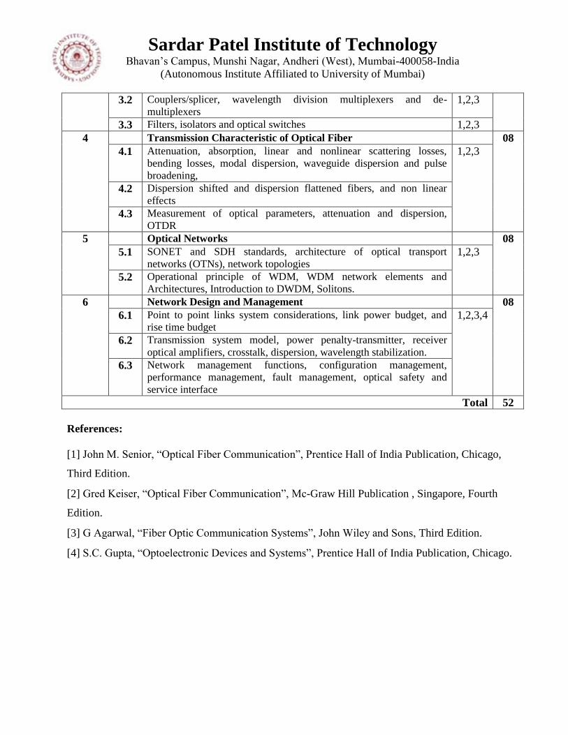
3.2 Couplers/splicer, wavelength division multiplexers and de-
multiplexers 1,2,3
3.3 Filters, isolators and optical switches 1,2,3
4 Transmission Characteristic of Optical Fiber 08
4.1 Attenuation, absorption, linear and nonlinear scattering losses,
bending losses, modal dispersion, waveguide dispersion and pulse
broadening,
1,2,3
4.2 Dispersion shifted and dispersion flattened fibers, and non linear
effects
4.3 Measurement of optical parameters, attenuation and dispersion,
OTDR
5 Optical Networks 08
5.1 SONET and SDH standards, architecture of optical transport
networks (OTNs), network topologies 1,2,3
5.2 Operational principle of WDM, WDM network elements and
Architectures, Introduction to DWDM, Solitons.
6 Network Design and Management 08
6.1 Point to point links system considerations, link power budget, and
rise time budget 1,2,3,4
6.2 Transmission system model, power penalty-transmitter, receiver
optical amplifiers, crosstalk, dispersion, wavelength stabilization.
6.3 Network management functions, configuration management,
performance management, fault management, optical safety and
service interface
Total 52
References:
[1] John M. Senior, “Optical Fiber Communication”, Prentice Hall of India Publication, Chicago,
Third Edition.
[2] Gred Keiser, “Optical Fiber Communication”, Mc-Graw Hill Publication , Singapore, Fourth
Edition.
[3] G Agarwal, “Fiber Optic Communication Systems”, John Wiley and Sons, Third Edition.
[4] S.C. Gupta, “Optoelectronic Devices and Systems”, Prentice Hall of India Publication, Chicago.
Sardar Patel Institute of Technology Bhavan‟s Campus, Munshi Nagar, Andheri (West), Mumbai-400058-India
(Autonomous Institute Affiliated to University of Mumbai)
Course
Code Course Name
Teaching Scheme
(Hrs/week) Credits Assigned
L T P L T P Total
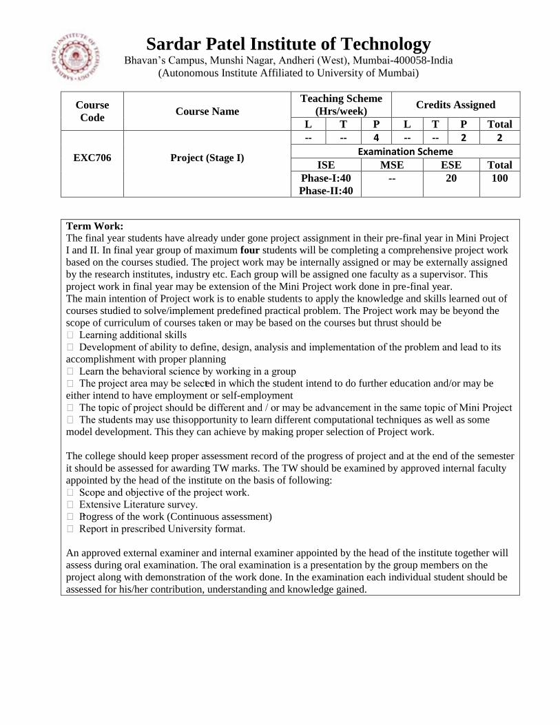
EXC706
Project (Stage I)
-- -- 4 -- -- 2 2
Examination Scheme ISE MSE ESE Total
Phase-I:40
Phase-II:40 -- 20 100
Term Work: The final year students have already under gone project assignment in their pre-final year in Mini Project
I and II. In final year group of maximum four students will be completing a comprehensive project work
based on the courses studied. The project work may be internally assigned or may be externally assigned
by the research institutes, industry etc. Each group will be assigned one faculty as a supervisor. This
project work in final year may be extension of the Mini Project work done in pre-final year.
The main intention of Project work is to enable students to apply the knowledge and skills learned out of
courses studied to solve/implement predefined practical problem. The Project work may be beyond the
scope of curriculum of courses taken or may be based on the courses but thrust should be
Learning additional skills
Development of ability to define, design, analysis and implementation of the problem and lead to its
accomplishment with proper planning
Learn the behavioral science by working in a group
The project area may be selected in which the student intend to do further education and/or may be
either intend to have employment or self-employment
The topic of project should be different and / or may be advancement in the same topic of Mini Project
The students may use this opportunity to learn different computational techniques as well as some
model development. This they can achieve by making proper selection of Project work.
The college should keep proper assessment record of the progress of project and at the end of the semester
it should be assessed for awarding TW marks. The TW should be examined by approved internal faculty
appointed by the head of the institute on the basis of following:
Scope and objective of the project work.
Extensive Literature survey.
Progress of the work (Continuous assessment)
Report in prescribed University format.
An approved external examiner and internal examiner appointed by the head of the institute together will
assess during oral examination. The oral examination is a presentation by the group members on the
project along with demonstration of the work done. In the examination each individual student should be
assessed for his/her contribution, understanding and knowledge gained.
Sardar Patel Institute of Technology Bhavan‟s Campus, Munshi Nagar, Andheri (West), Mumbai-400058-India
(Autonomous Institute Affiliated to University of Mumbai)
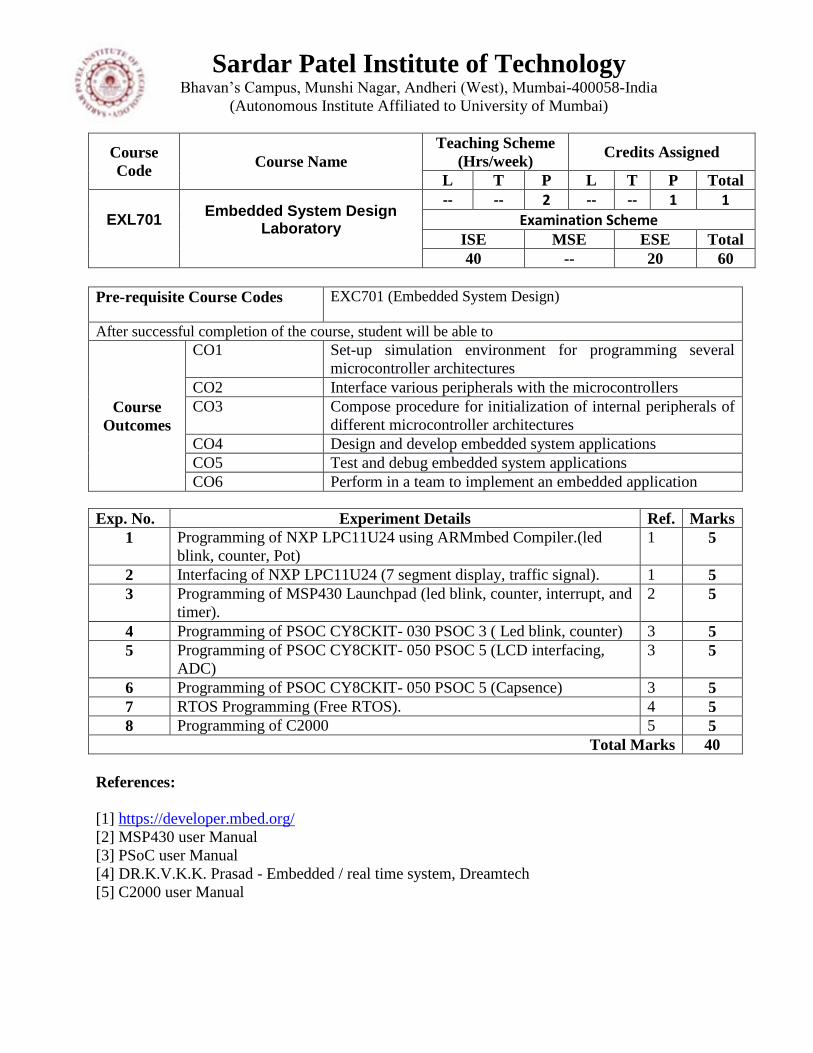
Course
Code Course Name
Teaching Scheme
(Hrs/week) Credits Assigned
L T P L T P Total
EXL701
Embedded System Design Laboratory
-- -- 2 -- -- 1 1
Examination Scheme ISE MSE ESE Total
40 -- 20 60
Pre-requisite Course Codes EXC701 (Embedded System Design)
After successful completion of the course, student will be able to
Course
Outcomes
CO1 Set-up simulation environment for programming several
microcontroller architectures
CO2 Interface various peripherals with the microcontrollers
CO3 Compose procedure for initialization of internal peripherals of
different microcontroller architectures
CO4 Design and develop embedded system applications
CO5 Test and debug embedded system applications
CO6 Perform in a team to implement an embedded application
Exp. No. Experiment Details Ref. Marks
1 Programming of NXP LPC11U24 using ARMmbed Compiler.(led
blink, counter, Pot)
1 5
2 Interfacing of NXP LPC11U24 (7 segment display, traffic signal). 1 5
3 Programming of MSP430 Launchpad (led blink, counter, interrupt, and
timer).
2 5
4 Programming of PSOC CY8CKIT- 030 PSOC 3 ( Led blink, counter) 3 5
5 Programming of PSOC CY8CKIT- 050 PSOC 5 (LCD interfacing,
ADC)
3 5
6 Programming of PSOC CY8CKIT- 050 PSOC 5 (Capsence) 3 5
7 RTOS Programming (Free RTOS). 4 5
8 Programming of C2000 5 5
Total Marks 40
References:
[1] https://developer.mbed.org/
[2] MSP430 user Manual
[3] PSoC user Manual
[4] DR.K.V.K.K. Prasad - Embedded / real time system, Dreamtech
[5] C2000 user Manual
Sardar Patel Institute of Technology Bhavan‟s Campus, Munshi Nagar, Andheri (West), Mumbai-400058-India
(Autonomous Institute Affiliated to University of Mumbai)
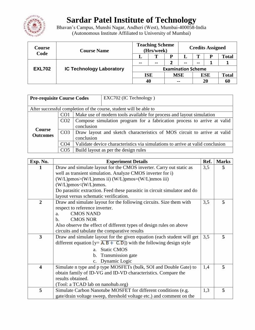
Course
Code Course Name
Teaching Scheme
(Hrs/week) Credits Assigned
L T P L T P Total
EXL702
IC Technology Laboratory
-- -- 2 -- -- 1 1
Examination Scheme ISE MSE ESE Total
40 -- 20 60
Pre-requisite Course Codes EXC702 (IC Technology )
After successful completion of the course, student will be able to
Course
Outcomes
CO1 Make use of modern tools available for process and layout simulation
CO2 Compose simulation program for a fabrication process to arrive at valid
conclusion
CO3 Draw layout and sketch characteristics of MOS circuit to arrive at valid
conclusion
CO4 Validate device characteristics via simulations to arrive at valid conclusion
CO5 Build layout as per the design rules
Exp. No. Experiment Details Ref. Marks
1 Draw and simulate layout for the CMOS inverter. Carry out static as
well as transient simulation. Analyze CMOS inverter for i)
(W/L)pmos>(W/L)nmos ii) (W/L)pmos=(W/L)nmos iii)
(W/L)pmos<(W/L)nmos.
Do parasitic extraction. Feed these parasitic in circuit simulator and do
layout versus schematic verification.
3,5 5
2 Draw and simulate layout for the following circuits. Size them with
respect to reference inverter.
a. CMOS NAND
b. CMOS NOR
Also observe the effect of different types of design rules on above
circuits and tabulate the comparative results
3,5 5
3 Draw and simulate layout for the given equation (each student will get
different equation [y= ]) with the following design style
a. Static CMOS
b. Transmission gate
c. Dynamic Logic
3,5 5
4 Simulate n type and p type MOSFETs (bulk, SOI and Double Gate) to
obtain family of ID-VG and ID-VD characteristics. Compare the
results obtained.
(Tool: a TCAD lab on nanohub.org)
1,4 5
5 Simulate Carbon Nanotube MOSFET for different conditions (e.g.
gate/drain voltage sweep, threshold voltage etc.) and comment on the
1,3 5
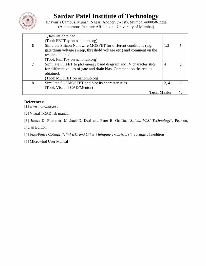
Sardar Patel Institute of Technology Bhavan‟s Campus, Munshi Nagar, Andheri (West), Mumbai-400058-India
(Autonomous Institute Affiliated to University of Mumbai)
1,3results obtained.
(Tool: FETToy on nanohub.org)
6 Simulate Silicon Nanowire MOSFET for different conditions (e.g.
gate/drain voltage sweep, threshold voltage etc.) and comment on the
results obtained.
(Tool: FETToy on nanohub.org)
1,3 5
7 Simulate FinFET to plot energy band diagram and IV characteristics
for different values of gate and drain bias. Comment on the results
obtained.
(Tool: MuGFET on nanohub.org)
4 5
8 Simulate SOI MOSFET and plot its characteristics.
(Tool: Visual TCAD/Mentor)
2, 4 5
Total Marks 40
References: [1] www.nanohub.org
[2] Visual TCAD lab manual
[3] James D. Plummer, Michael D. Deal and Peter B. Griffin, “Silicon VLSI Technology”, Pearson,
Indian Edition
[4] Jean-Pierre Colinge, “FinFETs and Other Multigate Transistors”, Springer, 1st edition
[5] Microwind User Manual
Sardar Patel Institute of Technology Bhavan‟s Campus, Munshi Nagar, Andheri (West), Mumbai-400058-India
(Autonomous Institute Affiliated to University of Mumbai)
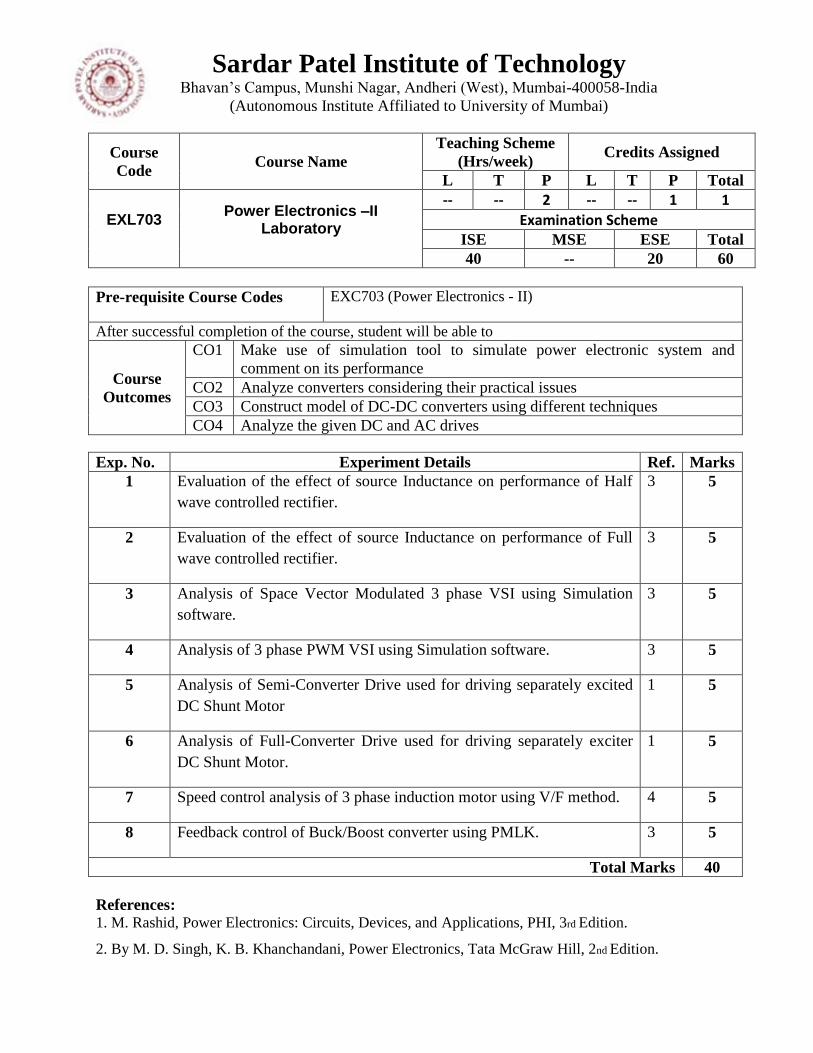
Course
Code Course Name
Teaching Scheme
(Hrs/week) Credits Assigned
L T P L T P Total
EXL703
Power Electronics –II Laboratory
-- -- 2 -- -- 1 1
Examination Scheme ISE MSE ESE Total
40 -- 20 60
Pre-requisite Course Codes EXC703 (Power Electronics - II)
After successful completion of the course, student will be able to
Course
Outcomes
CO1 Make use of simulation tool to simulate power electronic system and
comment on its performance
CO2 Analyze converters considering their practical issues
CO3 Construct model of DC-DC converters using different techniques
CO4 Analyze the given DC and AC drives
Exp. No. Experiment Details Ref. Marks
1 Evaluation of the effect of source Inductance on performance of Half
wave controlled rectifier.
3 5
2 Evaluation of the effect of source Inductance on performance of Full
wave controlled rectifier.
3 5
3 Analysis of Space Vector Modulated 3 phase VSI using Simulation
software.
3 5
4 Analysis of 3 phase PWM VSI using Simulation software. 3 5
5 Analysis of Semi-Converter Drive used for driving separately excited
DC Shunt Motor
1 5
6 Analysis of Full-Converter Drive used for driving separately exciter
DC Shunt Motor.
1 5
7 Speed control analysis of 3 phase induction motor using V/F method. 4 5
8 Feedback control of Buck/Boost converter using PMLK. 3 5
Total Marks 40
References: 1. M. Rashid, Power Electronics: Circuits, Devices, and Applications, PHI, 3rd Edition.
2. By M. D. Singh, K. B. Khanchandani, Power Electronics, Tata McGraw Hill, 2nd Edition.
Sardar Patel Institute of Technology Bhavan‟s Campus, Munshi Nagar, Andheri (West), Mumbai-400058-India
(Autonomous Institute Affiliated to University of Mumbai) 3. Mohan, Undeland and Riobbins, Power Electronics: Converters, Applications and Design, Wiley
(Student Edition), 2nd Edition.
4. P. S. Bimbhra, Power Electronics, Khanna Publishers, 2012.
5. R. W. Erickson, D. Maksimovic, Fundamentals of Power Electronics, Springer, 2nd Edition.
6. J. P. Agrawal, Power Electronics Systems: Theory and Design, Pearson Education, 2002.
7. S. Bacha, I. Munteanu and A. Bratcu, Power Electronic Converters: Modeling and Control, Springer-
Verlag, 2014.
8. H. Sira-Ramírez, R. Silva-Ortigoza, Control Design Techniques in Power Electronics Devices,
Springer-Verlag, 2006
Sardar Patel Institute of Technology Bhavan‟s Campus, Munshi Nagar, Andheri (West), Mumbai-400058-India
(Autonomous Institute Affiliated to University of Mumbai)
Course
Code Course Name
Teaching Scheme
(Hrs/week) Credits Assigned
L T P L T P Total
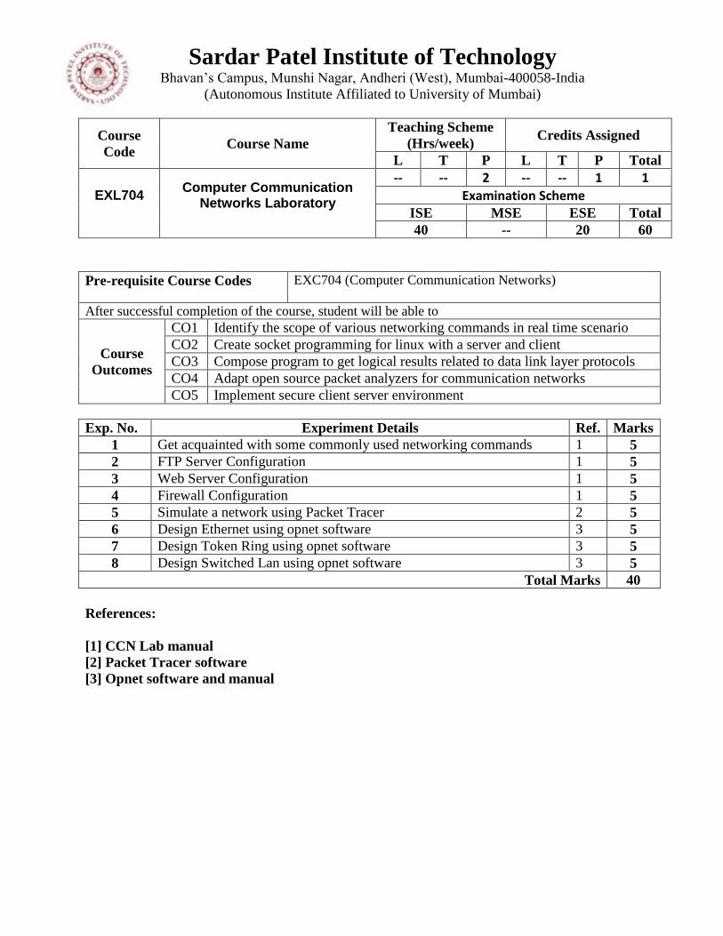
EXL704
Computer Communication Networks Laboratory
-- -- 2 -- -- 1 1
Examination Scheme ISE MSE ESE Total
40 -- 20 60
Pre-requisite Course Codes EXC704 (Computer Communication Networks)
After successful completion of the course, student will be able to
Course
Outcomes
CO1 Identify the scope of various networking commands in real time scenario
CO2 Create socket programming for linux with a server and client
CO3 Compose program to get logical results related to data link layer protocols
CO4 Adapt open source packet analyzers for communication networks
CO5 Implement secure client server environment
Exp. No. Experiment Details Ref. Marks
1 Get acquainted with some commonly used networking commands 1 5
2 FTP Server Configuration 1 5
3 Web Server Configuration 1 5
4 Firewall Configuration 1 5
5 Simulate a network using Packet Tracer 2 5
6 Design Ethernet using opnet software 3 5
7 Design Token Ring using opnet software 3 5
8 Design Switched Lan using opnet software 3 5
Total Marks 40
References:
[1] CCN Lab manual
[2] Packet Tracer software
[3] Opnet software and manual
Sardar Patel Institute of Technology Bhavan‟s Campus, Munshi Nagar, Andheri (West), Mumbai-400058-India
(Autonomous Institute Affiliated to University of Mumbai)
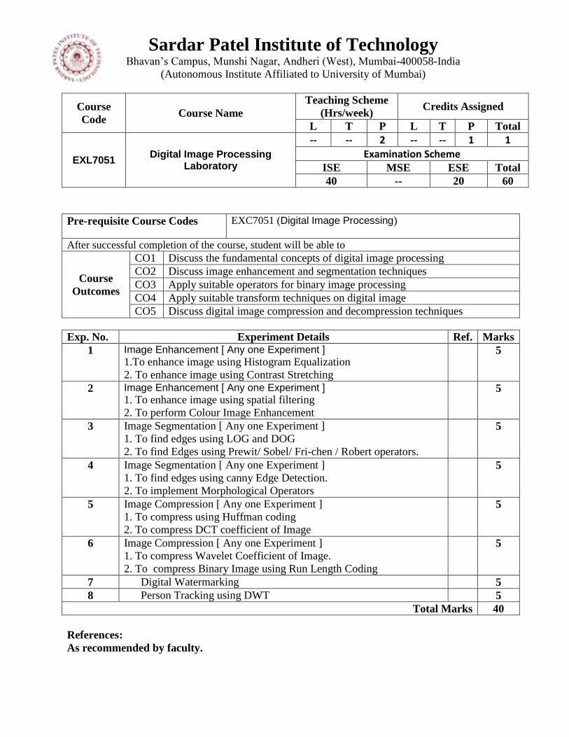
Course
Code Course Name
Teaching Scheme
(Hrs/week) Credits Assigned
L T P L T P Total
EXL7051 Digital Image Processing
Laboratory
-- -- 2 -- -- 1 1
Examination Scheme ISE MSE ESE Total
40 -- 20 60
Pre-requisite Course Codes EXC7051 (Digital Image Processing)
After successful completion of the course, student will be able to
Course
Outcomes
CO1 Discuss the fundamental concepts of digital image processing
CO2 Discuss image enhancement and segmentation techniques
CO3 Apply suitable operators for binary image processing
CO4 Apply suitable transform techniques on digital image
CO5 Discuss digital image compression and decompression techniques
Exp. No. Experiment Details Ref. Marks
1 Image Enhancement [ Any one Experiment ] 1.To enhance image using Histogram Equalization
2. To enhance image using Contrast Stretching
5
2 Image Enhancement [ Any one Experiment ] 1. To enhance image using spatial filtering
2. To perform Colour Image Enhancement
5
3 Image Segmentation [ Any one Experiment ]
1. To find edges using LOG and DOG
2. To find Edges using Prewit/ Sobel/ Fri-chen / Robert operators.
5
4 Image Segmentation [ Any one Experiment ]
1. To find edges using canny Edge Detection.
2. To implement Morphological Operators
5
5 Image Compression [ Any one Experiment ]
1. To compress using Huffman coding
2. To compress DCT coefficient of Image
5
6 Image Compression [ Any one Experiment ]
1. To compress Wavelet Coefficient of Image.
2. To compress Binary Image using Run Length Coding
5
7 Digital Watermarking 5
8 Person Tracking using DWT 5
Total Marks 40
References:
As recommended by faculty.
Sardar Patel Institute of Technology Bhavan‟s Campus, Munshi Nagar, Andheri (West), Mumbai-400058-India
(Autonomous Institute Affiliated to University of Mumbai)
Course
Code Course Name
Teaching Scheme
(Hrs/week) Credits Assigned
L T P L T P Total
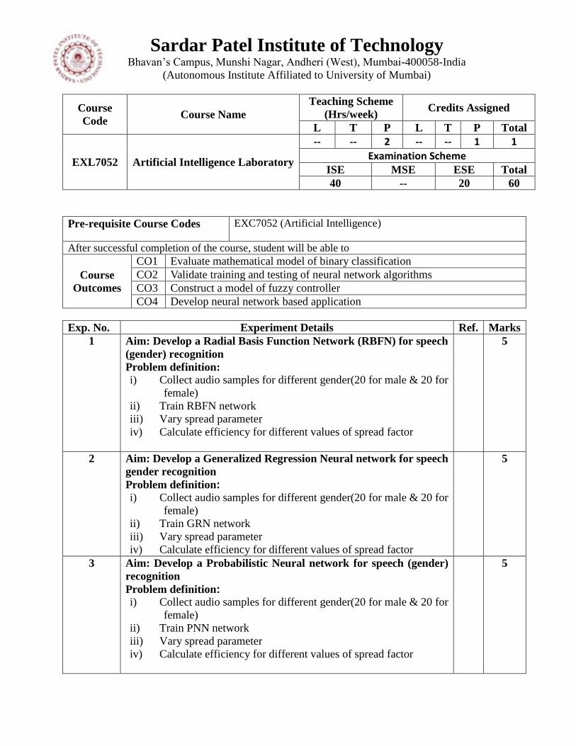
EXL7052 Artificial Intelligence Laboratory
-- -- 2 -- -- 1 1
Examination Scheme ISE MSE ESE Total
40 -- 20 60
Pre-requisite Course Codes EXC7052 (Artificial Intelligence)
After successful completion of the course, student will be able to
Course
Outcomes
CO1 Evaluate mathematical model of binary classification
CO2 Validate training and testing of neural network algorithms
CO3 Construct a model of fuzzy controller
CO4 Develop neural network based application
Exp. No. Experiment Details Ref. Marks
1 Aim: Develop a Radial Basis Function Network (RBFN) for speech
(gender) recognition
Problem definition:
i) Collect audio samples for different gender(20 for male & 20 for
female)
ii) Train RBFN network
iii) Vary spread parameter
iv) Calculate efficiency for different values of spread factor
5
2 Aim: Develop a Generalized Regression Neural network for speech
gender recognition
Problem definition: i) Collect audio samples for different gender(20 for male & 20 for
female)
ii) Train GRN network
iii) Vary spread parameter
iv) Calculate efficiency for different values of spread factor
5
3 Aim: Develop a Probabilistic Neural network for speech (gender)
recognition
Problem definition: i) Collect audio samples for different gender(20 for male & 20 for
female)
ii) Train PNN network
iii) Vary spread parameter
iv) Calculate efficiency for different values of spread factor
5
Sardar Patel Institute of Technology Bhavan‟s Campus, Munshi Nagar, Andheri (West), Mumbai-400058-India
(Autonomous Institute Affiliated to University of Mumbai)
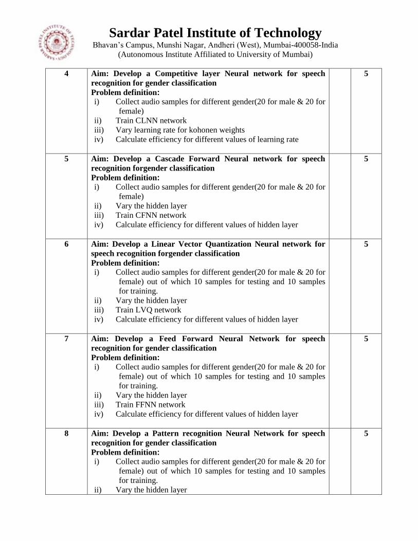
4 Aim: Develop a Competitive layer Neural network for speech
recognition for gender classification
Problem definition: i) Collect audio samples for different gender(20 for male & 20 for
female)
ii) Train CLNN network
iii) Vary learning rate for kohonen weights
iv) Calculate efficiency for different values of learning rate
5
5 Aim: Develop a Cascade Forward Neural network for speech
recognition forgender classification
Problem definition: i) Collect audio samples for different gender(20 for male & 20 for
female)
ii) Vary the hidden layer
iii) Train CFNN network
iv) Calculate efficiency for different values of hidden layer
5
6 Aim: Develop a Linear Vector Quantization Neural network for
speech recognition forgender classification
Problem definition: i) Collect audio samples for different gender(20 for male & 20 for
female) out of which 10 samples for testing and 10 samples
for training.
ii) Vary the hidden layer
iii) Train LVQ network
iv) Calculate efficiency for different values of hidden layer
5
7 Aim: Develop a Feed Forward Neural Network for speech
recognition for gender classification
Problem definition: i) Collect audio samples for different gender(20 for male & 20 for
female) out of which 10 samples for testing and 10 samples
for training.
ii) Vary the hidden layer
iii) Train FFNN network
iv) Calculate efficiency for different values of hidden layer
5
8 Aim: Develop a Pattern recognition Neural Network for speech
recognition for gender classification
Problem definition: i) Collect audio samples for different gender(20 for male & 20 for
female) out of which 10 samples for testing and 10 samples
for training.
ii) Vary the hidden layer
5
Sardar Patel Institute of Technology Bhavan‟s Campus, Munshi Nagar, Andheri (West), Mumbai-400058-India
(Autonomous Institute Affiliated to University of Mumbai)
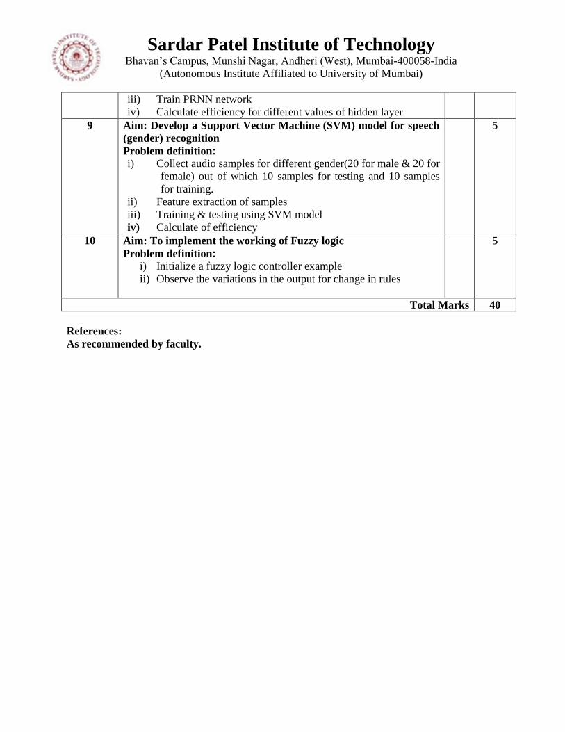
iii) Train PRNN network
iv) Calculate efficiency for different values of hidden layer
9 Aim: Develop a Support Vector Machine (SVM) model for speech
(gender) recognition
Problem definition: i) Collect audio samples for different gender(20 for male & 20 for
female) out of which 10 samples for testing and 10 samples
for training.
ii) Feature extraction of samples
iii) Training & testing using SVM model
iv) Calculate of efficiency
5
10 Aim: To implement the working of Fuzzy logic
Problem definition: i) Initialize a fuzzy logic controller example
ii) Observe the variations in the output for change in rules
5
Total Marks 40
References:
As recommended by faculty.
Sardar Patel Institute of Technology Bhavan‟s Campus, Munshi Nagar, Andheri (West), Mumbai-400058-India
(Autonomous Institute Affiliated to University of Mumbai)
Course
Code Course Name
Teaching Scheme
(Hrs/week) Credits Assigned
L T P L T P Total
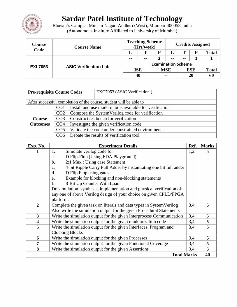
EXL7053 ASIC Verification Lab
-- -- 2 -- -- 1 1
Examination Scheme ISE MSE ESE Total
40 -- 20 60
Pre-requisite Course Codes EXC7053 (ASIC Verification )
After successful completion of the course, student will be able to
Course
Outcomes
CO1 Install and use modern tools available for verification
CO2 Compose the SystemVerilog code for verification
CO3 Construct testbench for verification
CO4 Investigate the given verification code
CO5 Validate the code under constrained environments
CO6 Debate the results of verification tool
Exp. No. Experiment Details Ref. Marks
1 1. Simulate verilog code for
a. D Flip-Flop (Using EDA Playground)
b. 2:1 Mux : Using case Statement
c. 4-bit Ripple Carry Full Adder by instantiating one bit full adder
d. D Flip Flop using gates
e. Example for blocking and non-blocking statements
f. 8-Bit Up Counter With Load
Do simulation, synthesis, implementation and physical verification of
any one of above Verilog design of your choice on given CPLD/FPGA
platform.
1,2 5
2 Complete the given task on literals and data types in SystemVerilog
Also write the simulation output for the given Procedural Statements
3,4 5
3 Write the simulation output for the given Interprocess Communication 3,4 5
4 Write the simulation output for the given randomization code 3,4 5
5 Write the simulation output for the given Interfaces, Program and
Clocking Blocks
3,4 5
6 Write the simulation output for the given Processes 3,4 5
7 Write the simulation output for the given Functional Coverage 3,4 5
8 Write the simulation output for the given Assertions 3,4 5
Total Marks 40
Sardar Patel Institute of Technology Bhavan‟s Campus, Munshi Nagar, Andheri (West), Mumbai-400058-India
(Autonomous Institute Affiliated to University of Mumbai)
References:
[1] Spartan and Virtex family user manuals from Xilinx
[2]Verilog Language Reference manual
[3]System Verilog Language Reference manual
[4] Chris Spear, “System Verilog for Verification: A guide to learning the testbench language
features”, Springer, 2nd Edition
Sardar Patel Institute of Technology Bhavan‟s Campus, Munshi Nagar, Andheri (West), Mumbai-400058-India
(Autonomous Institute Affiliated to University of Mumbai)
Course
Code Course Name
Teaching Scheme
(Hrs/week) Credits Assigned
L T P L T P Total
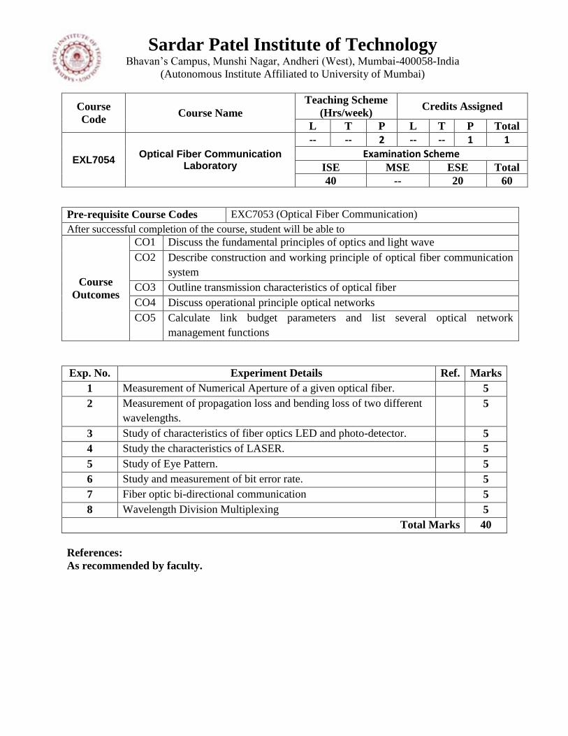
EXL7054 Optical Fiber Communication
Laboratory
-- -- 2 -- -- 1 1
Examination Scheme ISE MSE ESE Total
40 -- 20 60
Pre-requisite Course Codes EXC7053 (Optical Fiber Communication)
After successful completion of the course, student will be able to
Course
Outcomes
CO1 Discuss the fundamental principles of optics and light wave
CO2 Describe construction and working principle of optical fiber communication
system
CO3 Outline transmission characteristics of optical fiber
CO4 Discuss operational principle optical networks
CO5 Calculate link budget parameters and list several optical network
management functions
Exp. No. Experiment Details Ref. Marks
1 Measurement of Numerical Aperture of a given optical fiber. 5
2 Measurement of propagation loss and bending loss of two different
wavelengths.
5
3 Study of characteristics of fiber optics LED and photo-detector. 5
4 Study the characteristics of LASER. 5
5 Study of Eye Pattern. 5
6 Study and measurement of bit error rate. 5
7 Fiber optic bi-directional communication 5
8 Wavelength Division Multiplexing 5
Total Marks 40
References:
As recommended by faculty.
Sardar Patel Institute of Technology Bhavan‟s Campus, Munshi Nagar, Andheri (West), Mumbai-400058-India
(Autonomous Institute Affiliated to University of Mumbai)
Semester VIII
Sardar Patel Institute of Technology Bhavan‟s Campus, Munshi Nagar, Andheri (West), Mumbai-400058-India
(Autonomous Institute Affiliated to University of Mumbai)
Course
Code Course Name
Teaching
Scheme
(Hrs/week)
Credits Assigned
L T P L T P Total
EXC801 CMOS VLSI Design
4 -- -- 4 -- -- 4
Examination Scheme
ISE MSE ESE Total
20 20 60 100
Pre-requisite Course Codes EXC302: Electronic Devices EXC303: Digital Circuits and Design
EXC402: Discrete Electronic Circuits
EXC502: Design With Linear Integrated Circuits
EXC601: VLSI Design
EXC702: IC Technology
After successful completion of the course, student will be able to
Course
Outcomes
CO1 Recognize tradeoffs involved in analog VLSI Circuits
CO2 Analyze basic building blocks of CMOS analog VLSI circuits
CO3 Evaluate MOSFET based single stage and differential amplifiers
CO4 Design MOSFET based operational amplifier
CO5 Analyze mixed signal circuits
CO6 Describe layout techniques for analog circuits
Module
No.
Unit
No. Topics Ref. Hrs.
1 CMOS analog building blocks 08
1.1 MOS Models: Necessity of CMOS analog design, Review of
characteristics of MOS device, MOS small signal model, MOS spice
models
1
1.2 Passive and Active Current Mirrors: Basic current mirrors, Cascode
current mirrors and Active current mirrors 1
1.3 Band Gap References: General Considerations, Supply-independent
biasing, Temperature independent references, PTAT current generation
and Constant Gm biasing
1
2 Single Stage Amplifiers 10
2.1 Configurations: Basic concepts, Common source stage, Source
follower, Common gate stage, Cascode stage 1
2.2 Frequency Response and Noise: General considerations, Common-
source stage, Source followers, Common-gate stage, Cascode stage and
Noise in single stage amplifiers
1
3 Differential Amplifiers 10
3.1 Configurations: Single ended and differential operation, Basic
differential pair, Common-mode response, Differential pair with MOS
loads, Gilbert cell
1
3.2 Frequency response and noise in differential pair 1
Sardar Patel Institute of Technology Bhavan‟s Campus, Munshi Nagar, Andheri (West), Mumbai-400058-India
(Autonomous Institute Affiliated to University of Mumbai)
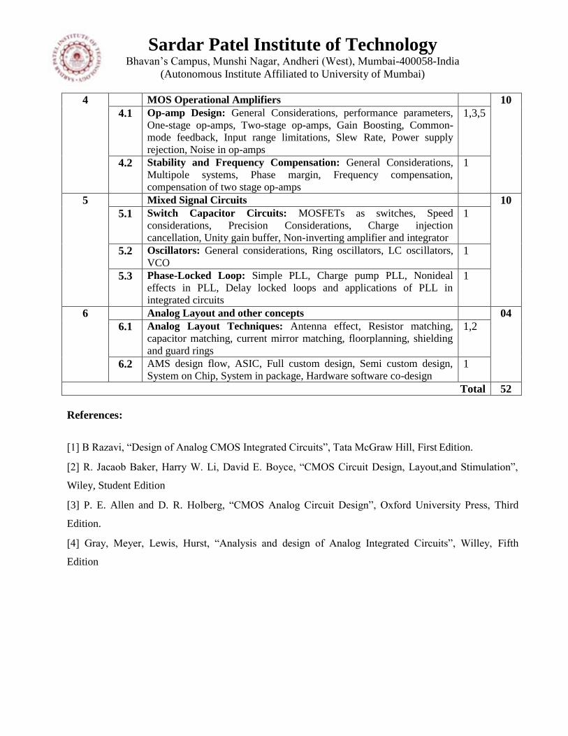
4 MOS Operational Amplifiers 10
4.1 Op-amp Design: General Considerations, performance parameters,
One-stage op-amps, Two-stage op-amps, Gain Boosting, Common-
mode feedback, Input range limitations, Slew Rate, Power supply
rejection, Noise in op-amps
1,3,5
4.2 Stability and Frequency Compensation: General Considerations,
Multipole systems, Phase margin, Frequency compensation,
compensation of two stage op-amps
1
5 Mixed Signal Circuits 10
5.1 Switch Capacitor Circuits: MOSFETs as switches, Speed
considerations, Precision Considerations, Charge injection
cancellation, Unity gain buffer, Non-inverting amplifier and integrator
1
5.2 Oscillators: General considerations, Ring oscillators, LC oscillators,
VCO 1
5.3 Phase-Locked Loop: Simple PLL, Charge pump PLL, Nonideal
effects in PLL, Delay locked loops and applications of PLL in
integrated circuits
1
6 Analog Layout and other concepts 04
6.1 Analog Layout Techniques: Antenna effect, Resistor matching,
capacitor matching, current mirror matching, floorplanning, shielding
and guard rings
1,2
6.2 AMS design flow, ASIC, Full custom design, Semi custom design,
System on Chip, System in package, Hardware software co-design 1
Total 52
References:
[1] B Razavi, “Design of Analog CMOS Integrated Circuits”, Tata McGraw Hill, First Edition.
[2] R. Jacaob Baker, Harry W. Li, David E. Boyce, “CMOS Circuit Design, Layout,and Stimulation”,
Wiley, Student Edition
[3] P. E. Allen and D. R. Holberg, “CMOS Analog Circuit Design”, Oxford University Press, Third
Edition.
[4] Gray, Meyer, Lewis, Hurst, “Analysis and design of Analog Integrated Circuits”, Willey, Fifth
Edition
Sardar Patel Institute of Technology Bhavan‟s Campus, Munshi Nagar, Andheri (West), Mumbai-400058-India
(Autonomous Institute Affiliated to University of Mumbai)
Course
Code Course Name
Teaching
Scheme
(Hrs/week)
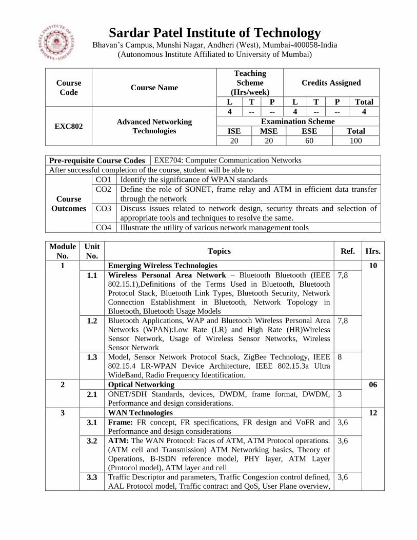
Credits Assigned
L T P L T P Total
EXC802 Advanced Networking
Technologies
4 -- -- 4 -- -- 4
Examination Scheme
ISE MSE ESE Total
20 20 60 100
Pre-requisite Course Codes EXE704: Computer Communication Networks
After successful completion of the course, student will be able to
Course
Outcomes
CO1 Identify the significance of WPAN standards
CO2 Define the role of SONET, frame relay and ATM in efficient data transfer
through the network
CO3 Discuss issues related to network design, security threats and selection of
appropriate tools and techniques to resolve the same.
CO4 Illustrate the utility of various network management tools
Module
No.
Unit
No. Topics Ref. Hrs.
1 Emerging Wireless Technologies 10
1.1 Wireless Personal Area Network – Bluetooth Bluetooth (IEEE
802.15.1),Definitions of the Terms Used in Bluetooth, Bluetooth
Protocol Stack, Bluetooth Link Types, Bluetooth Security, Network
Connection Establishment in Bluetooth, Network Topology in
Bluetooth, Bluetooth Usage Models
7,8
1.2 Bluetooth Applications, WAP and Bluetooth Wireless Personal Area
Networks (WPAN):Low Rate (LR) and High Rate (HR)Wireless
Sensor Network, Usage of Wireless Sensor Networks, Wireless
Sensor Network
7,8
1.3 Model, Sensor Network Protocol Stack, ZigBee Technology, IEEE
802.15.4 LR-WPAN Device Architecture, IEEE 802.15.3a Ultra
WideBand, Radio Frequency Identification.
8
2 Optical Networking 06
2.1 ONET/SDH Standards, devices, DWDM, frame format, DWDM,
Performance and design considerations. 3
3 WAN Technologies 12
3.1 Frame: FR concept, FR specifications, FR design and VoFR and
Performance and design considerations 3,6
3.2 ATM: The WAN Protocol: Faces of ATM, ATM Protocol operations.
(ATM cell and Transmission) ATM Networking basics, Theory of
Operations, B-ISDN reference model, PHY layer, ATM Layer
(Protocol model), ATM layer and cell
3,6
3.3 Traffic Descriptor and parameters, Traffic Congestion control defined,
AAL Protocol model, Traffic contract and QoS, User Plane overview, 3,6
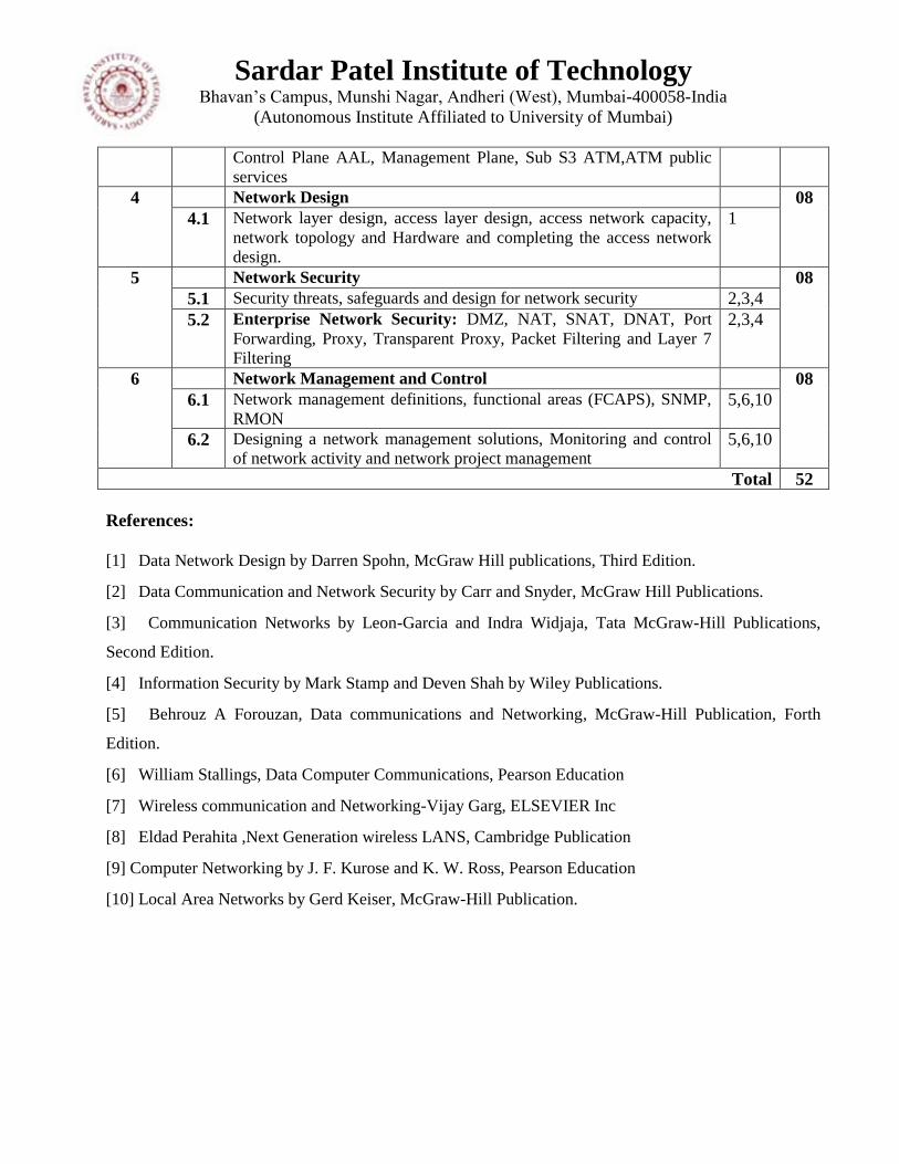
Sardar Patel Institute of Technology Bhavan‟s Campus, Munshi Nagar, Andheri (West), Mumbai-400058-India
(Autonomous Institute Affiliated to University of Mumbai)
Control Plane AAL, Management Plane, Sub S3 ATM,ATM public
services
4 Network Design 08
4.1 Network layer design, access layer design, access network capacity,
network topology and Hardware and completing the access network
design.
1
5 Network Security 08
5.1 Security threats, safeguards and design for network security 2,3,4
5.2 Enterprise Network Security: DMZ, NAT, SNAT, DNAT, Port
Forwarding, Proxy, Transparent Proxy, Packet Filtering and Layer 7
Filtering
2,3,4
6 Network Management and Control 08
6.1 Network management definitions, functional areas (FCAPS), SNMP,
RMON 5,6,10
6.2 Designing a network management solutions, Monitoring and control
of network activity and network project management 5,6,10
Total 52
References:
[1] Data Network Design by Darren Spohn, McGraw Hill publications, Third Edition.
[2] Data Communication and Network Security by Carr and Snyder, McGraw Hill Publications.
[3] Communication Networks by Leon-Garcia and Indra Widjaja, Tata McGraw-Hill Publications,
Second Edition.
[4] Information Security by Mark Stamp and Deven Shah by Wiley Publications.
[5] Behrouz A Forouzan, Data communications and Networking, McGraw-Hill Publication, Forth
Edition.
[6] William Stallings, Data Computer Communications, Pearson Education
[7] Wireless communication and Networking-Vijay Garg, ELSEVIER Inc
[8] Eldad Perahita ,Next Generation wireless LANS, Cambridge Publication
[9] Computer Networking by J. F. Kurose and K. W. Ross, Pearson Education
[10] Local Area Networks by Gerd Keiser, McGraw-Hill Publication.
Sardar Patel Institute of Technology Bhavan‟s Campus, Munshi Nagar, Andheri (West), Mumbai-400058-India
(Autonomous Institute Affiliated to University of Mumbai)
Course
Code Course Name
Teaching
Scheme
(Hrs/week)
Credits Assigned
L T P L T P Total
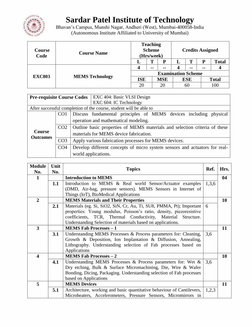
EXC803 MEMS Technology
4 -- -- 4 -- -- 4
Examination Scheme
ISE MSE ESE Total
20 20 60 100
Pre-requisite Course Codes EXC 404: Basic VLSI Design
EXC 604: IC Technology
After successful completion of the course, student will be able to
Course
Outcomes
CO1 Discuss fundamental principles of MEMS devices including physical
operation and mathematical modeling.
CO2 Outline basic properties of MEMS materials and selection criteria of these
materials for MEMS device fabrication.
CO3 Apply various fabrication processes for MEMS devices.
CO4 Develop different concepts of micro system sensors and actuators for real-
world applications.
Module
No.
Unit
No. Topics Ref. Hrs.
1 Introduction to MEMS 04
1.1 Introduction to MEMS & Real world Sensor/Actuator examples
(DMD, Air-bag, pressure sensors). MEMS Sensors in Internet of
Things (IoT), BioMedical Applications
1,3,6
2 MEMS Materials and Their Properties 10
2.1 Materials (eg. Si, SiO2, SiN, Cr, Au, Ti, SU8, PMMA, Pt); Important
properties: Young modulus, Poisson‟s ratio, density, piezoresistive
coefficients, TCR, Thermal Conductivity, Material Structure.
Understanding Selection of materials based on applications.
6
3 MEMS Fab Processes – 1 11
3.1 Understanding MEMS Processes & Process parameters for: Cleaning,
Growth & Deposition, Ion Implantation & Diffusion, Annealing,
Lithography. Understanding selection of Fab processes based on
Applications
3,6
4 MEMS Fab Processes – 2 10
4.1 Understanding MEMS Processes & Process parameters for: Wet &
Dry etching, Bulk & Surface Micromachining, Die, Wire & Wafer
Bonding, Dicing, Packaging. Understanding selection of Fab processes
based on Applications
3,6
5 MEMS Devices 11
5.1 Architecture, working and basic quantitative behaviour of Cantilevers,
Microheaters, Accelerometers, Pressure Sensors, Micromirrors in 1,2,3
Sardar Patel Institute of Technology Bhavan‟s Campus, Munshi Nagar, Andheri (West), Mumbai-400058-India
(Autonomous Institute Affiliated to University of Mumbai)
DMD, Inkjet printer-head. Understanding steps involved in Fabricating
above devices
6 MEMS Device Characterization 06
6.1 Piezoresistance, TCR, Stiffness, Adhesion, Vibration, Resonant
frequency, & importance of these measurements in studying device
behavior, MEMS Reliability
6
Total 52
References:
[1] N. Maluf, K Williams,”An Introduction to Microelectromechanical Systems Engineering” Artech
House Inc, Second Edition.
[2] Practical MEMS - by Ville Kaajakari; Publisher: Small Gear Publishing
[3] Microsystem Design - by S. Senturia; Publisher: Springer
[4] Analysis and Design Principles of MEMS Devices - Minhang Bao; Publisher: Elsevier Science
[5] Fundamentals of Microfabrication - by M. Madou; Publisher: CRC Press; Second edition
[6] Micro Electro Mechanical System Design - by J. Allen; Publisher: CRC Press
[7] Micromachined Transducers Sourcebook - by G. Kovacs; Publisher: McGraw-Hill
Sardar Patel Institute of Technology Bhavan‟s Campus, Munshi Nagar, Andheri (West), Mumbai-400058-India
(Autonomous Institute Affiliated to University of Mumbai)
Course
Code Course Name
Teaching
Scheme
(Hrs/week)
Credits Assigned
L T P L T P Total
EXC8041 Robotics
4 -- -- 4 -- -- 4
Examination Scheme
ISE MSE ESE Total
20 20 60 100
Pre-requisite Course Codes EXS 301 : Applied Mathematics III EXS 401 : Applied Mathematics IV
EXC 404 : Principles of Control Systems
After successful completion of the course, student will be able to
Course
Outcomes
CO1 Discuss the fundamentals of robotics.
CO2 Apply the direct and inverse kinematics algorithm for robotic arm
manipulation
CO3 Analyse the equations for velocity kinematics and Dynamics.
CO4 Discuss the concept of robot motion planning using different algorithms.
CO5 Justify the need of trajectory planning and robot vision algorithms for robotic
arm manipulation
Module
No.
Unit
No. Topics Ref. Hrs.
1 Fundamentals of Robotics 03
1.1 Robot Classification, Robot Components, Degrees of freedom, Joints,
Coordinates, Coordinate frames, workspace, applications 1
2 Forward & Inverse Kinematics of Robots 09
2.1 Homogeneous transformation matrices, Inverse transformation
matrices, Forward and inverse kinematic equations – position and
orientation
2
2.2 Denavit-Hatenberg representation of forward kinematics, Inverse
kinematic solutions, Case studies 2
3 Velocity Kinematics & Dynamics 14
3.1 Differential motions and velocities : Differential relationship,
Jacobian, Differential motion of a frame and robot, Inverse
Jacobian,Singularities.
2
3.2 Dynamic Analysis of Forces : Lagrangian mechanics, Newton Euler
formulation, Dynamic equations of robots, Transformation of forces
and moment between coordinate frames
2
4 Robot Motion Planning 04
4.1 Concept of motion planning, Bug Algorithms – Bug1, Bug2, Tangent
Bug 3
5 Potential Functions and Visibility Graphs 08
5.1 Attractive/Repulsive potential, Gradient descent, wave-front planner,
navigation potential functions, Visibility map, Generalized Voronoi 3
Sardar Patel Institute of Technology Bhavan‟s Campus, Munshi Nagar, Andheri (West), Mumbai-400058-India
(Autonomous Institute Affiliated to University of Mumbai)
diagrams and graphs, Silhouette methods
6 Trajectory Planning 08
6.1 Trajectory planning, Joint-space trajectory planning, Cartesian-space
trajectories 2
7 Robot Vision 06
7.1 Image representation, Template matching, Polyhedral objects, Shape
analysis, Segmentation, Iterative processing, Perspective transform. 1
Total 52
References:
[1] Robert Shilling, Fundamentals of Robotics - Analysis and control, Prentice Hall of India
[2] Saeed Benjamin Niku, “Introduction to Robotics – Analysis, Control, Applications”, Wiley India
Pvt. Ltd., Second Edition.
[3] Howie Choset, Kevin M. Lynch, Seth Hutchinson, George Kantor, Wolfram Burgard, Lydia E.
Kavraki and Sebastian Thrun, “Principles of Robot Motion – Theory, Algorithms and
Implementations”, Prentice-Hall of India.
[4] Mark W. Spong , Seth Hutchinson, M. Vidyasagar, “Robot Modeling & Control ”, Wiley India
Pvt. Ltd.
[5] John J. Craig, “Introduction to Robotics – Mechanics & Control”, Third Edition, Pearson
Education, India.
[6] Aaron Martinez & Enrique Fernandez, “Learning ROS for Robotics Programming”, Shroff
Publishers, First Edition.
[7] Mikell P. Groover et.al, ”Industrial Robots-Technology, Programming & applications” ,McGraw
Hill , New York.
Sardar Patel Institute of Technology Bhavan‟s Campus, Munshi Nagar, Andheri (West), Mumbai-400058-India
(Autonomous Institute Affiliated to University of Mumbai)
Course
Code Course Name
Teaching
Scheme
(Hrs/week)
Credits Assigned
L T P L T P Total
EXC8042 Mobile Communication
4 -- -- 4 -- -- 4
Examination Scheme
ISE MSE ESE Total
20 20 60 100
Pre-requisite Course Codes EXC 704: Computer Communication Networks
EXC: Digital Communication
After successful completion of the course, student will be able to
Course
Outcomes
CO1 Identify the blocks of cellular communication system
CO2 Compare GSM and CDMA standards
CO3 Explain 3G mobile communication system
CO4 Identify the requirements of 4G standards
CO5 Discuss emerging technologies
Module
No.
Unit
No. Topics Ref. Hrs.
1 Cellular Communication System 10
1.1 Introduction to Cellular Communications, Frequency reuse, Multiple
Access Technologies 1,2
1.2 Cellular Processes: Channel assignment, Call Setup, Handoff strategies,
interferences and system capacity 1
1.3 Traffic Theory: Trunking and grade of service, improving system
capacity 1
2 GSM 08
2.1 GSM Network architecture, signaling protocol architecture, identifiers,
channels, Frame structure, speech coding, authentication and security, call
procedure, handoff procedure, services and features
1
3 CDMA digital cellular standard (1S-95). 08
3.1 Frequency and channel specifications of IS-95, forward and reverse
CDMA channel, packet and frame formats, mobility and radio resource
management
1
4 3 G Mobile Communication System 10
4.1 2.5 G TDMA Evolution Path, GPRS, EDGE , 2.5G CDMA one cellular
N/W, Need of 3G Cellular N/w, IMT 2000 Global Standard, UMTS
Technology, W-CDMA Air interface, TD-SCDMA Technology, CDMA
2000 Cellular Technology
4
5 4G Wireless Standards 08
5.1 Need for 4G network, difference between 3G and 4G, LTE, WiMAX 4
6 Emerging Technologies 08
6.1 Mobile Adhoc Network, Mobile IP and Mobility Management, Mobile
TCP, Wireless Sensor Networks, RFID Technology 4
Total 52
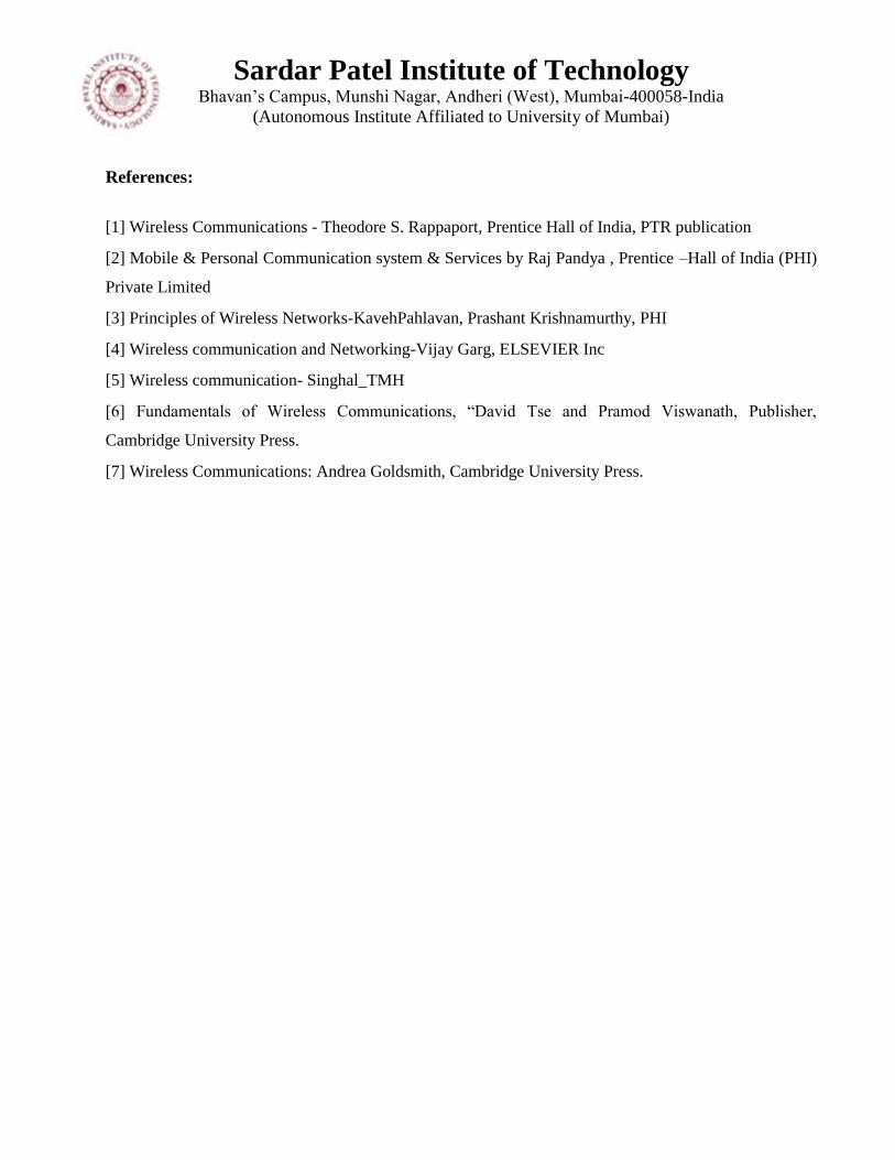
Sardar Patel Institute of Technology Bhavan‟s Campus, Munshi Nagar, Andheri (West), Mumbai-400058-India
(Autonomous Institute Affiliated to University of Mumbai)
References:
[1] Wireless Communications - Theodore S. Rappaport, Prentice Hall of India, PTR publication
[2] Mobile & Personal Communication system & Services by Raj Pandya , Prentice –Hall of India (PHI)
Private Limited
[3] Principles of Wireless Networks-KavehPahlavan, Prashant Krishnamurthy, PHI
[4] Wireless communication and Networking-Vijay Garg, ELSEVIER Inc
[5] Wireless communication- Singhal_TMH
[6] Fundamentals of Wireless Communications, “David Tse and Pramod Viswanath, Publisher,
Cambridge University Press.
[7] Wireless Communications: Andrea Goldsmith, Cambridge University Press.
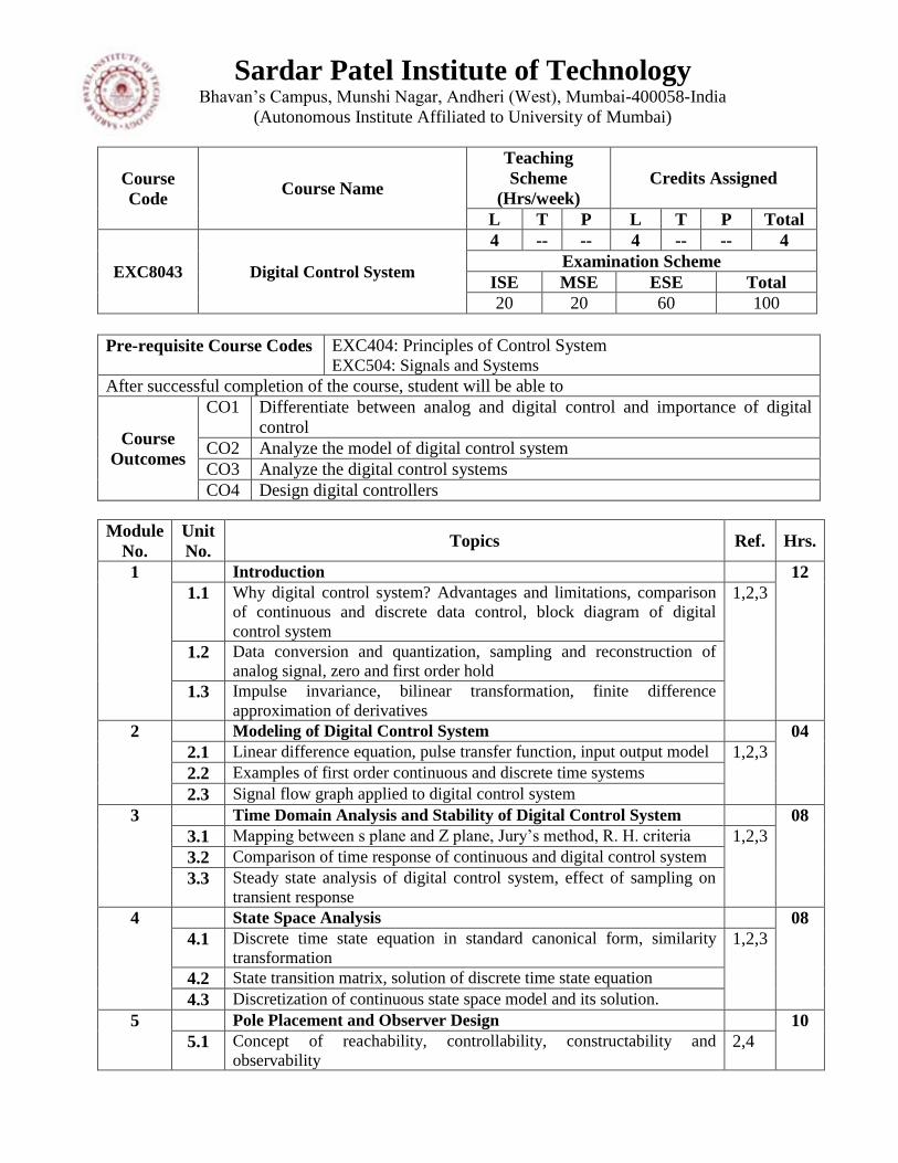
Sardar Patel Institute of Technology Bhavan‟s Campus, Munshi Nagar, Andheri (West), Mumbai-400058-India
(Autonomous Institute Affiliated to University of Mumbai)
Course
Code Course Name
Teaching
Scheme
(Hrs/week)
Credits Assigned
L T P L T P Total
EXC8043 Digital Control System
4 -- -- 4 -- -- 4
Examination Scheme
ISE MSE ESE Total
20 20 60 100
Pre-requisite Course Codes EXC404: Principles of Control System EXC504: Signals and Systems
After successful completion of the course, student will be able to
Course
Outcomes
CO1 Differentiate between analog and digital control and importance of digital
control
CO2 Analyze the model of digital control system
CO3 Analyze the digital control systems
CO4 Design digital controllers
Module
No.
Unit
No. Topics Ref. Hrs.
1 Introduction 12
1.1 Why digital control system? Advantages and limitations, comparison
of continuous and discrete data control, block diagram of digital
control system
1,2,3
1.2 Data conversion and quantization, sampling and reconstruction of
analog signal, zero and first order hold
1.3 Impulse invariance, bilinear transformation, finite difference
approximation of derivatives
2 Modeling of Digital Control System 04
2.1 Linear difference equation, pulse transfer function, input output model 1,2,3
2.2 Examples of first order continuous and discrete time systems
2.3 Signal flow graph applied to digital control system
3 Time Domain Analysis and Stability of Digital Control System 08
3.1 Mapping between s plane and Z plane, Jury‟s method, R. H. criteria 1,2,3
3.2 Comparison of time response of continuous and digital control system
3.3 Steady state analysis of digital control system, effect of sampling on
transient response
4 State Space Analysis 08
4.1 Discrete time state equation in standard canonical form, similarity
transformation 1,2,3
4.2 State transition matrix, solution of discrete time state equation
4.3 Discretization of continuous state space model and its solution.
5 Pole Placement and Observer Design 10
5.1 Concept of reachability, controllability, constructability and
observability 2,4
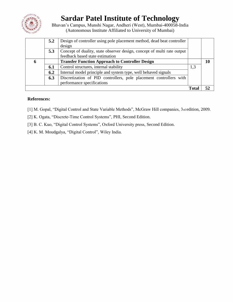
Sardar Patel Institute of Technology Bhavan‟s Campus, Munshi Nagar, Andheri (West), Mumbai-400058-India
(Autonomous Institute Affiliated to University of Mumbai)
5.2 Design of controller using pole placement method, dead beat controller
design
5.3 Concept of duality, state observer design, concept of multi rate output
feedback based state estimation
6 Transfer Function Approach to Controller Design 10
6.1 Control structures, internal stability 1,3
6.2 Internal model principle and system type, well behaved signals
6.3 Discretization of PID controllers, pole placement controllers with
performance specifications
Total 52
References:
[1] M. Gopal, “Digital Control and State Variable Methods”, McGraw Hill companies, 3rd edition, 2009.
[2] K. Ogata, “Discrete-Time Control Systems”, PHI, Second Edition.
[3] B. C. Kuo, “Digital Control Systems”, Oxford University press, Second Edition.
[4] K. M. Moudgalya, “Digital Control”, Wiley India.
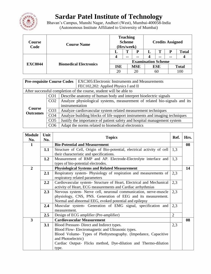
Sardar Patel Institute of Technology Bhavan‟s Campus, Munshi Nagar, Andheri (West), Mumbai-400058-India
(Autonomous Institute Affiliated to University of Mumbai)
Course
Code Course Name
Teaching
Scheme
(Hrs/week)
Credits Assigned
L T P L T P Total
EXC8044 Biomedical Electronics
4 -- -- 4 -- -- 4
Examination Scheme
ISE MSE ESE Total
20 20 60 100
Pre-requisite Course Codes EXC305:Electronic Instruments and Measurements FEC102,202: Applied Physics I and II
After successful completion of the course, student will be able to
Course
Outcomes
CO1 Describe anatomy of human body and interpret bioelectric signals
CO2 Analyze physiological systems, measurement of related bio-signals and its
instrumentation
CO3 Analyze cardiovascular system related measurement techniques
CO4 Analyze building blocks of life support instruments and imaging techniques
CO5 Justify the importance of patient safety and hospital management system
CO6 Adapt the norms related to biomedical electronics
Module
No.
Unit
No. Topics Ref. Hrs.
1 Bio-Potential and Measurement 08
1.1 Structure of Cell, Origin of Bio-potential, electrical activity of cell
their characteristic and specifications. 1,3
1.2 Measurement of RMP and AP. Electrode-Electrolyte interface and
types of bio-potential electrodes. 1,3
2 Physiological Systems and Related Measurement 14
2.1 Respiratory system- Physiology of respiration and measurements of
respiratory related parameters 2,3
2.2 Cardiovascular system- Structure of Heart, Electrical and Mechanical
activity of Heart, ECG measurements and Cardiac arrhythmias 2,3
2.3 Nervous system- Nerve cell, neuronal communication, nerve-muscle
physiology, CNS, PNS. Generation of EEG and its measurement.
Normal and abnormal EEG, evoked potential and epilepsy
2,3
2.4 Muscular system- Generation of EMG signal, specification and
measurement. 2,3
2.5 Design of ECG amplifier (Pre-amplifier) 2
3 Cardiovascular Measurement 08
3.1 Blood Pressure- Direct and Indirect types.
Blood Flow- Electromagnetic and Ultrasonic types.
Blood Volume- Types of Plethysmography. (Impedance, Capacitive
and Photoelectric)
Cardiac Output- Flicks method, Dye-dilution and Thermo-dilution
type.
2,3
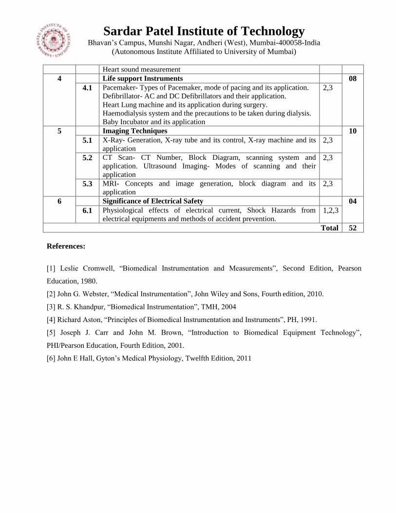
Sardar Patel Institute of Technology Bhavan‟s Campus, Munshi Nagar, Andheri (West), Mumbai-400058-India
(Autonomous Institute Affiliated to University of Mumbai)
Heart sound measurement
4 Life support Instruments 08
4.1 Pacemaker- Types of Pacemaker, mode of pacing and its application.
Defibrillator- AC and DC Defibrillators and their application.
Heart Lung machine and its application during surgery.
Haemodialysis system and the precautions to be taken during dialysis.
Baby Incubator and its application
2,3
5 Imaging Techniques 10
5.1 X-Ray- Generation, X-ray tube and its control, X-ray machine and its
application 2,3
5.2 CT Scan- CT Number, Block Diagram, scanning system and
application. Ultrasound Imaging- Modes of scanning and their
application
2,3
5.3 MRI- Concepts and image generation, block diagram and its
application 2,3
6 Significance of Electrical Safety 04
6.1 Physiological effects of electrical current, Shock Hazards from
electrical equipments and methods of accident prevention. 1,2,3
Total 52
References:
[1] Leslie Cromwell, “Biomedical Instrumentation and Measurements”, Second Edition, Pearson
Education, 1980.
[2] John G. Webster, “Medical Instrumentation”, John Wiley and Sons, Fourth edition, 2010.
[3] R. S. Khandpur, “Biomedical Instrumentation”, TMH, 2004
[4] Richard Aston, “Principles of Biomedical Instrumentation and Instruments”, PH, 1991.
[5] Joseph J. Carr and John M. Brown, “Introduction to Biomedical Equipment Technology”,
PHI/Pearson Education, Fourth Edition, 2001.
[6] John E Hall, Gyton‟s Medical Physiology, Twelfth Edition, 2011
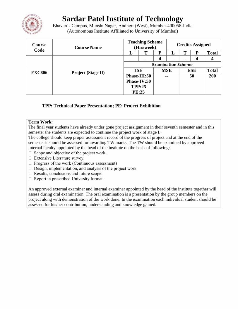
Sardar Patel Institute of Technology Bhavan‟s Campus, Munshi Nagar, Andheri (West), Mumbai-400058-India
(Autonomous Institute Affiliated to University of Mumbai)
Course
Code Course Name
Teaching Scheme
(Hrs/week) Credits Assigned
L T P L T P Total
EXC806
Project (Stage II)
-- -- 4 -- -- 4 4
Examination Scheme ISE MSE ESE Total
Phase-III:50
Phase-IV:50
TPP:25
PE:25
-- 50 200
TPP: Technical Paper Presentation; PE: Project Exhibition
Term Work: The final year students have already under gone project assignment in their seventh semester and in this
semester the students are expected to continue the project work of stage I.
The college should keep proper assessment record of the progress of project and at the end of the
semester it should be assessed for awarding TW marks. The TW should be examined by approved
internal faculty appointed by the head of the institute on the basis of following:
Scope and objective of the project work.
Extensive Literature survey.
Progress of the work (Continuous assessment)
Design, implementation, and analysis of the project work.
Results, conclusions and future scope.
Report in prescribed University format.
An approved external examiner and internal examiner appointed by the head of the institute together will
assess during oral examination. The oral examination is a presentation by the group members on the
project along with demonstration of the work done. In the examination each individual student should be
assessed for his/her contribution, understanding and knowledge gained.
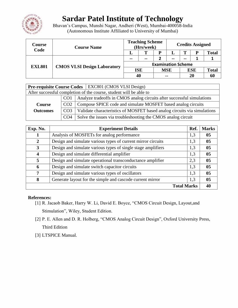
Sardar Patel Institute of Technology Bhavan‟s Campus, Munshi Nagar, Andheri (West), Mumbai-400058-India
(Autonomous Institute Affiliated to University of Mumbai)
Course
Code Course Name
Teaching Scheme
(Hrs/week) Credits Assigned
L T P L T P Total
EXL801 CMOS VLSI Design Laboratory
-- -- 2 -- -- 1 1
Examination Scheme ISE MSE ESE Total
40 -- 20 60
Pre-requisite Course Codes EXC801 (CMOS VLSI Design)
After successful completion of the course, student will be able to
Course
Outcomes
CO1 Analyze tradeoffs in CMOS analog circuits after successful simulations
CO2 Compose SPICE code and simulate MOSFET based analog circuits
CO3 Validate characteristics of MOSFET based analog circuits via simulations
CO4 Solve the issues via troubleshooting the CMOS analog circuit
Exp. No. Experiment Details Ref. Marks
1 Analysis of MOSFETs for analog performance 1,3 05
2 Design and simulate various types of current mirror circuits 1,3 05
3 Design and simulate various types of single stage amplifiers 1,3 05
4 Design and simulate differential amplifier 1,3 05
5 Design and simulate operational transconductance amplifier 2,3 05
6 Design and simulate switch capacitor circuits 1,3 05
7 Design and simulate various types of oscillators 1,3 05
8 Generate layout for the simple and cascode current mirror 1,3 05
Total Marks 40
References:
[1] R. Jacaob Baker, Harry W. Li, David E. Boyce, “CMOS Circuit Design, Layout,and
Stimulation”, Wiley, Student Edition.
[2] P. E. Allen and D. R. Holberg, “CMOS Analog Circuit Design”, Oxford University Press,
Third Edition
[3] LTSPICE Manual.
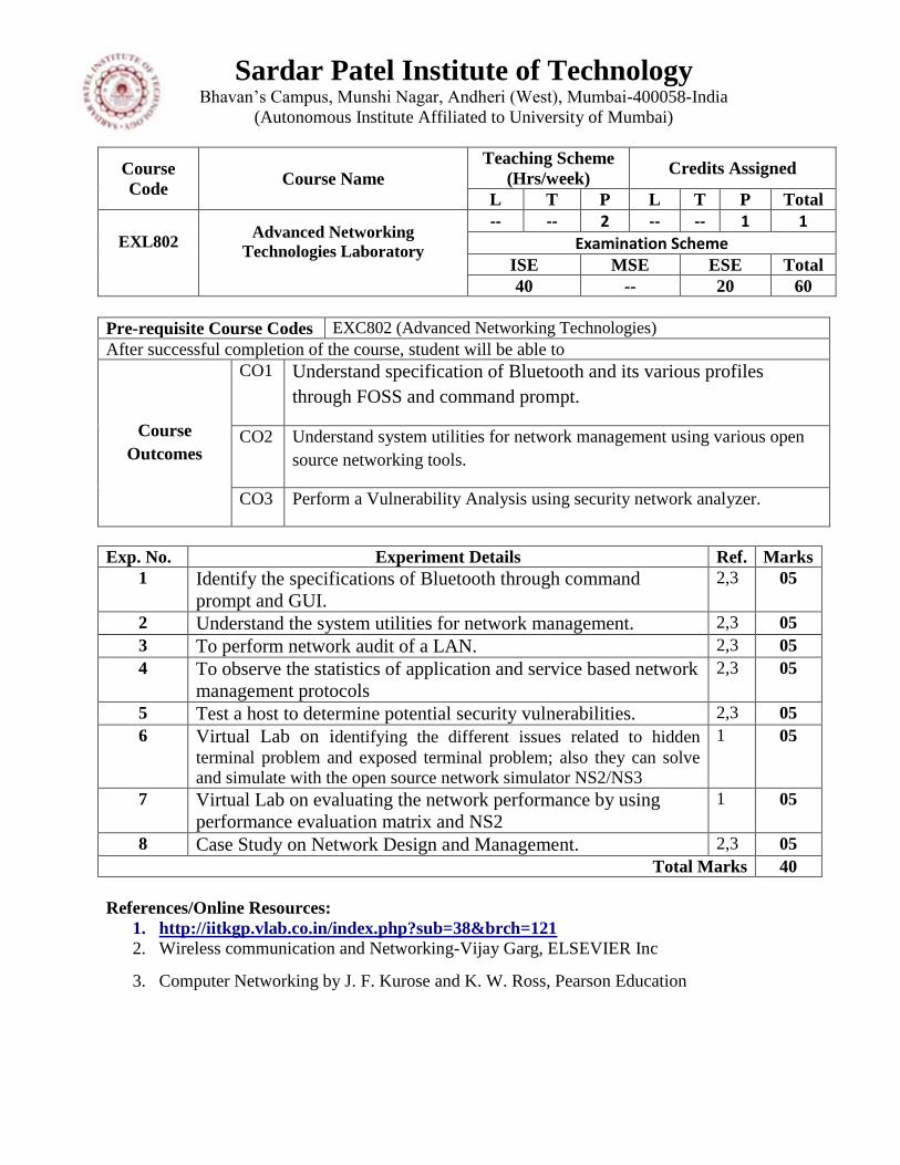
Sardar Patel Institute of Technology Bhavan‟s Campus, Munshi Nagar, Andheri (West), Mumbai-400058-India
(Autonomous Institute Affiliated to University of Mumbai)
Course
Code Course Name
Teaching Scheme
(Hrs/week) Credits Assigned
L T P L T P Total
EXL802
Advanced Networking
Technologies Laboratory
-- -- 2 -- -- 1 1
Examination Scheme ISE MSE ESE Total
40 -- 20 60
Pre-requisite Course Codes EXC802 (Advanced Networking Technologies)
After successful completion of the course, student will be able to
Course
Outcomes
CO1 Understand specification of Bluetooth and its various profiles
through FOSS and command prompt.
CO2 Understand system utilities for network management using various open
source networking tools.
CO3 Perform a Vulnerability Analysis using security network analyzer.
Exp. No. Experiment Details Ref. Marks
1 Identify the specifications of Bluetooth through command
prompt and GUI.
2,3 05
2 Understand the system utilities for network management. 2,3 05
3 To perform network audit of a LAN. 2,3 05
4 To observe the statistics of application and service based network
management protocols
2,3 05
5 Test a host to determine potential security vulnerabilities. 2,3 05
6 Virtual Lab on identifying the different issues related to hidden
terminal problem and exposed terminal problem; also they can solve
and simulate with the open source network simulator NS2/NS3
1 05
7 Virtual Lab on evaluating the network performance by using
performance evaluation matrix and NS2
1 05
8 Case Study on Network Design and Management. 2,3 05
Total Marks 40
References/Online Resources:
1. http://iitkgp.vlab.co.in/index.php?sub=38&brch=121
2. Wireless communication and Networking-Vijay Garg, ELSEVIER Inc
3. Computer Networking by J. F. Kurose and K. W. Ross, Pearson Education
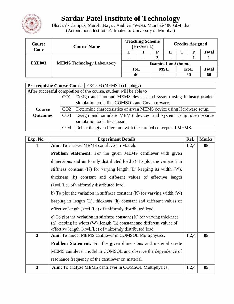
Sardar Patel Institute of Technology Bhavan‟s Campus, Munshi Nagar, Andheri (West), Mumbai-400058-India
(Autonomous Institute Affiliated to University of Mumbai)
Course
Code Course Name
Teaching Scheme
(Hrs/week) Credits Assigned
L T P L T P Total
EXL803
MEMS Technology Laboratory
-- -- 2 -- -- 1 1
Examination Scheme ISE MSE ESE Total
40 -- 20 60
Pre-requisite Course Codes EXC803 (MEMS Technology)
After successful completion of the course, student will be able to
Course
Outcomes
CO1 Design and simulate MEMS devices and system using Industry graded
simulation tools like COMSOL and Coventorware.
CO2 Determine characteristics of given MEMS device using Hardware setup.
CO3 Design and simulate MEMS devices and system using open source
simulation tools like sugar.
CO4 Relate the given literature with the studied concepts of MEMS.
Exp. No. Experiment Details Ref. Marks
1 Aim: To analyze MEMS cantilever in Matlab.
Problem Statement: For the given MEMS cantilever with given
dimensions and uniformly distributed load a) To plot the variation in
stiffness constant (K) for varying length (L) keeping its width (W),
thickness (h) constant and different values of effective length
(λr=L/Lc) of uniformly distributed load.
b) To plot the variation in stiffness constant (K) for varying width (W)
keeping its length (L), thickness (h) constant and different values of
effective length (λr=L/Lc) of uniformly distributed load.
c) To plot the variation in stiffness constant (K) for varying thickness
(h) keeping its width (W), length (L) constant and different values of
effective length (λr=L/Lc) of uniformly distributed load
1,2,4 05
2 Aim: To model MEMS cantilever in COMSOL Multiphysics.
Problem Statement: For the given dimensions and material create
MEMS cantilever model in COMSOL and observe the dependence of
resonance frequency of the cantilever on material.
1,2,4 05
3 Aim: To analyze MEMS cantilever in COMSOL Multiphysics. 1,2,4 05
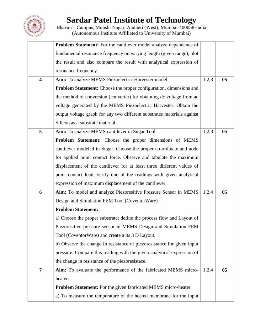
Sardar Patel Institute of Technology Bhavan‟s Campus, Munshi Nagar, Andheri (West), Mumbai-400058-India
(Autonomous Institute Affiliated to University of Mumbai)
Problem Statement: For the cantilever model analyze dependence of
fundamental resonance frequency on varying length (given range), plot
the result and also compare the result with analytical expression of
resonance frequency.
4 Aim: To analyze MEMS Piezoelectric Harvester model.
Problem Statement: Choose the proper configuration, dimensions and
the method of conversion (converter) for obtaining dc voltage from ac
voltage generated by the MEMS Piezoelectric Harvester. Obtain the
output voltage graph for any two different substrates materials against
Silicon as a substrate material.
1,2,3 05
5 Aim: To analyze MEMS cantilever in Sugar Tool.
Problem Statement: Choose the proper dimensions of MEMS
cantilever modeled in Sugar. Choose the proper co-ordinate and node
for applied point contact force. Observe and tabulate the maximum
displacement of the cantilever for at least three different values of
point contact load, verify one of the readings with given analytical
expression of maximum displacement of the cantilever.
1,2,3 05
6 Aim: To model and analyze Piezoresitive Pressure Sensor in MEMS
Design and Simulation FEM Tool (CoventorWare).
Problem Statement:
a) Choose the proper substrate; define the process flow and Layout of
Piezoresitive pressure sensor in MEMS Design and Simulation FEM
Tool (CoventorWare) and create a its 3 D Layout.
b) Observe the change in resistance of piezoresistance for given input
pressure. Compare this reading with the given analytical expression of
the change in resistance of the piezoresistace.
1,2,4 05
7 Aim: To evaluate the performance of the fabricated MEMS micro-
heater.
Problem Statement: For the given fabricated MEMS micro-heater,
a) To measure the temperature of the heated membrane for the input
1,2,4 05
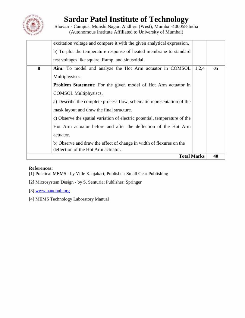
Sardar Patel Institute of Technology Bhavan‟s Campus, Munshi Nagar, Andheri (West), Mumbai-400058-India
(Autonomous Institute Affiliated to University of Mumbai)
excitation voltage and compare it with the given analytical expression.
b) To plot the temperature response of heated membrane to standard
test voltages like square, Ramp, and sinusoidal.
8 Aim: To model and analyze the Hot Arm actuator in COMSOL
Multiphysiscs.
Problem Statement: For the given model of Hot Arm actuator in
COMSOL Multiphysiscs,
a) Describe the complete process flow, schematic representation of the
mask layout and draw the final structure.
c) Observe the spatial variation of electric potential, temperature of the
Hot Arm actuator before and after the deflection of the Hot Arm
actuator.
b) Observe and draw the effect of change in width of flexures on the
deflection of the Hot Arm actuator.
1,2,4 05
Total Marks 40
References: [1] Practical MEMS - by Ville Kaajakari; Publisher: Small Gear Publishing
[2] Microsystem Design - by S. Senturia; Publisher: Springer
[3] www.nanohub.org
[4] MEMS Technology Laboratory Manual
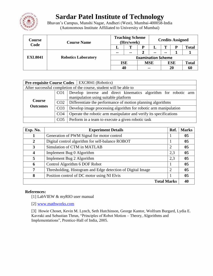
Sardar Patel Institute of Technology Bhavan‟s Campus, Munshi Nagar, Andheri (West), Mumbai-400058-India
(Autonomous Institute Affiliated to University of Mumbai)
Course
Code Course Name
Teaching Scheme
(Hrs/week) Credits Assigned
L T P L T P Total
EXL8041
Robotics Laboratory
-- -- 2 -- -- 1 1
Examination Scheme ISE MSE ESE Total
40 -- 20 60
Pre-requisite Course Codes EXC8041 (Robotics)
After successful completion of the course, student will be able to
Course
Outcomes
CO1 Develop inverse and direct kinematics algorithm for robotic arm
manipulation using suitable platform
CO2 Differentiate the performance of motion planning algorithms
CO3 Develop image processing algorithm for robotic arm manipulation
CO4 Operate the robotic arm manipulator and verify its specifications
CO5 Perform in a team to execute a given robotic task
Exp. No. Experiment Details Ref. Marks
1 Generation of PWM Signal for motor control 1 05
2 Digital control algorithm for self-balance ROBOT 1 05
3 Simulation of CTM in MATLAB 2 05
4 Implement Bug 0 Algorithm 2,3 05
5 Implement Bug 2 Algorithm 2,3 05
6 Control Algorithm 6 DOF Robot 1 05
7 Thresholding, Histogram and Edge detection of Digital Image 2 05
8 Position control of DC motor using NI Elvis 1 05
Total Marks 40
References:
[1] LabVIEW & myRIO user manual
[2] www.mathworks.com
[3] Howie Choset, Kevin M. Lynch, Seth Hutchinson, George Kantor, Wolfram Burgard, Lydia E.
Kavraki and Sebastian Thrun, “Principles of Robot Motion – Theory, Algorithms and
Implementations”, Prentice-Hall of India, 2005.
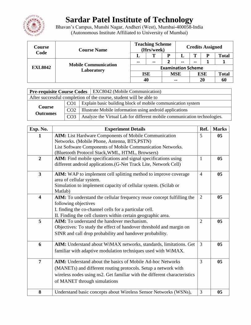
Sardar Patel Institute of Technology Bhavan‟s Campus, Munshi Nagar, Andheri (West), Mumbai-400058-India
(Autonomous Institute Affiliated to University of Mumbai)
Course
Code Course Name
Teaching Scheme
(Hrs/week) Credits Assigned
L T P L T P Total
EXL8042
Mobile Communication
Laboratory
-- -- 2 -- -- 1 1
Examination Scheme ISE MSE ESE Total
40 -- 20 60
Pre-requisite Course Codes EXC8042 (Mobile Communication)
After successful completion of the course, student will be able to
Course
Outcomes
CO1 Explain basic building block of mobile communication system
CO2 Illustrate Mobile information using android applications
CO3 Analyze the Virtual Lab for different mobile communication technologies.
Exp. No. Experiment Details Ref. Marks
1 AIM: List Hardware Components of Mobile Communication
Networks. (Mobile Phone, Antenna, BTS,PSTN)
List Software Components of Mobile Communication Networks.
(Bluetooth Protocol Stack,WML, HTML, Browsers)
5 05
2 AIM: Find mobile specifications and signal specifications using
different android applications.(G-Net Track Lite, Network Cell)
1 05
3 AIM: WAP to implement cell splitting method to improve coverage
area of cellular system.
Simulation to implement capacity of cellular system. (Scilab or
Matlab)
4 05
4 AIM: To understand the cellular frequency reuse concept fulfilling the
following objectives
I. finding the co-channel cells for a particular cell.
II. Finding the cell clusters within certain geographic area.
2 05
5 AIM: To understand the handover mechanism.
Objectives: To study the effect of handover threshold and margin on
SINR and call drop probability and handover probability.
2 05
6 AIM: Understand about WiMAX networks, standards, limitations. Get
familiar with adaptive modulation techniques used with WiMAX.
3 05
7 AIM: Understand about the basics of Mobile Ad-hoc Networks
(MANETs) and different routing protocols. Setup a network with
wireless nodes using ns2. Get familiar with the different characteristics
of MANET through simulations
3 05
8 Understand basic concepts about Wireless Sensor Networks (WSNs), 3 05
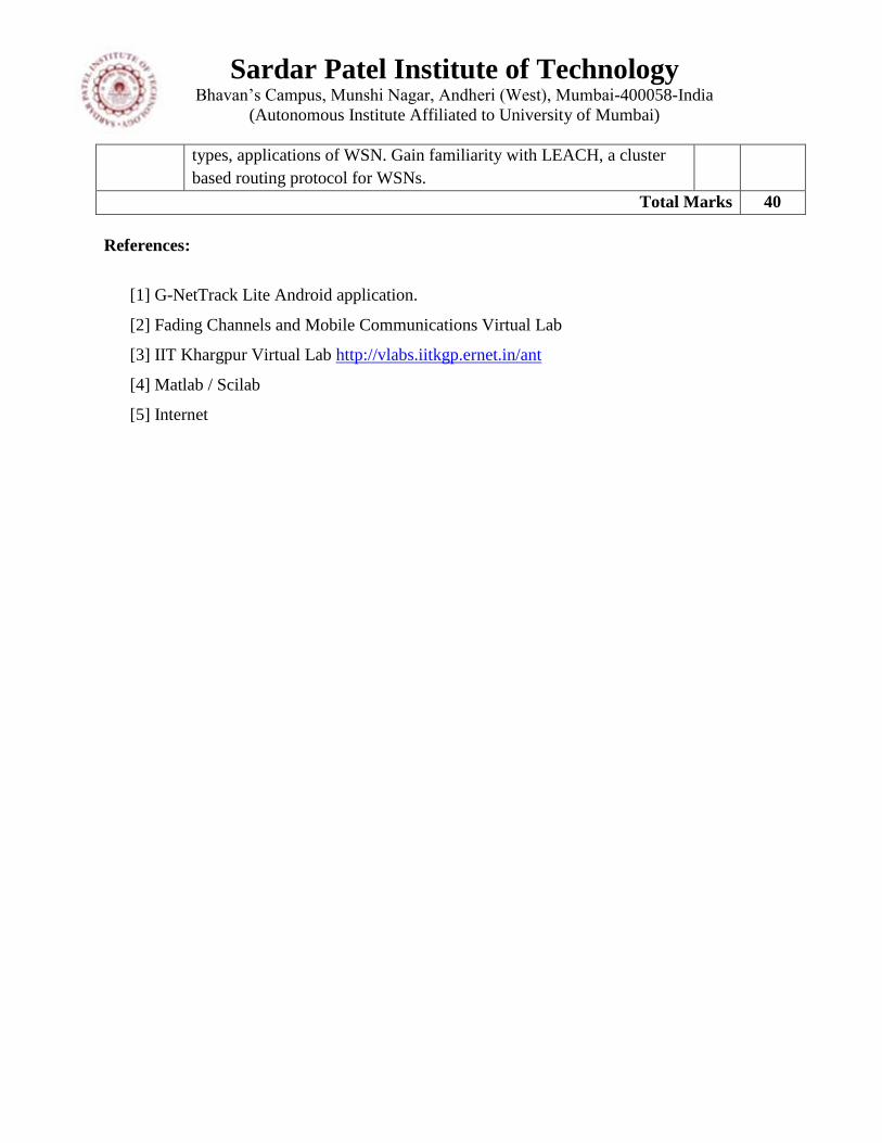
Sardar Patel Institute of Technology Bhavan‟s Campus, Munshi Nagar, Andheri (West), Mumbai-400058-India
(Autonomous Institute Affiliated to University of Mumbai)
types, applications of WSN. Gain familiarity with LEACH, a cluster
based routing protocol for WSNs.
Total Marks 40
References:
[1] G-NetTrack Lite Android application.
[2] Fading Channels and Mobile Communications Virtual Lab
[3] IIT Khargpur Virtual Lab http://vlabs.iitkgp.ernet.in/ant
[4] Matlab / Scilab
[5] Internet
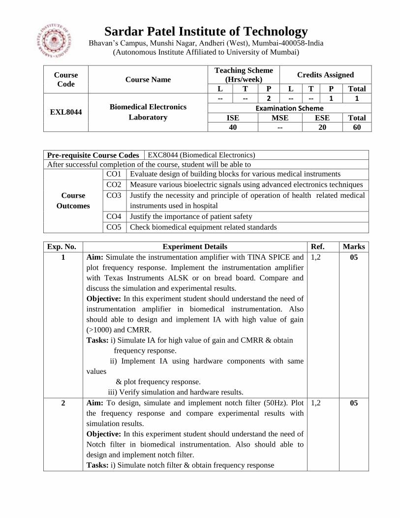
Sardar Patel Institute of Technology Bhavan‟s Campus, Munshi Nagar, Andheri (West), Mumbai-400058-India
(Autonomous Institute Affiliated to University of Mumbai)
Course
Code Course Name
Teaching Scheme
(Hrs/week) Credits Assigned
L T P L T P Total
EXL8044 Biomedical Electronics
Laboratory
-- -- 2 -- -- 1 1
Examination Scheme ISE MSE ESE Total
40 -- 20 60
Pre-requisite Course Codes EXC8044 (Biomedical Electronics)
After successful completion of the course, student will be able to
Course
Outcomes
CO1 Evaluate design of building blocks for various medical instruments
CO2 Measure various bioelectric signals using advanced electronics techniques
CO3 Justify the necessity and principle of operation of health related medical
instruments used in hospital
CO4 Justify the importance of patient safety
CO5 Check biomedical equipment related standards
Exp. No. Experiment Details Ref. Marks
1 Aim: Simulate the instrumentation amplifier with TINA SPICE and
plot frequency response. Implement the instrumentation amplifier
with Texas Instruments ALSK or on bread board. Compare and
discuss the simulation and experimental results.
Objective: In this experiment student should understand the need of
instrumentation amplifier in biomedical instrumentation. Also
should able to design and implement IA with high value of gain
(>1000) and CMRR.
Tasks: i) Simulate IA for high value of gain and CMRR & obtain
frequency response.
ii) Implement IA using hardware components with same
values
& plot frequency response.
iii) Verify simulation and hardware results.
1,2 05
2 Aim: To design, simulate and implement notch filter (50Hz). Plot
the frequency response and compare experimental results with
simulation results.
Objective: In this experiment student should understand the need of
Notch filter in biomedical instrumentation. Also should able to
design and implement notch filter.
Tasks: i) Simulate notch filter & obtain frequency response
1,2 05
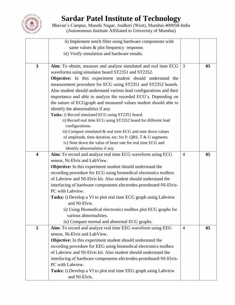
Sardar Patel Institute of Technology Bhavan‟s Campus, Munshi Nagar, Andheri (West), Mumbai-400058-India
(Autonomous Institute Affiliated to University of Mumbai)
ii) Implement notch filter using hardware components with
same values & plot frequency response.
iii) Verify simulation and hardware results.
3 Aim: To obtain, measure and analyze simulated and real time ECG
waveforms using simulator board ST2351 and ST2352.
Objective: In this experiment student should understand the
measurement procedure for ECG using ST2351 and ST2352 boards.
Also student should understand various lead configurations and their
importance and able to analyze the recorded ECG‟s. Depending on
the nature of ECGgraph and measured values student should able to
identify the abnormalities if any.
Tasks: i) Record simulated ECG using ST2351 board.
ii) Record real time ECG using ST2352 board for different lead
configurations.
iii) Compare simulated & real time ECG and note down values
of amplitude, time duration, etc; for P, QRS, T & U segments.
iv) Note down the value of heart rate for real time ECG and
identify abnormalities if any.
3 05
4 Aim: To record and analyze real time ECG waveform using ECG
sensor, Ni-Elvis and LabView.
Objective: In this experiment student should understand the
recording procedure for ECG using biomedical electronics toolbox
of Labview and NI-Elvis kit. Also student should understand the
interfacing of hardware components electrodes-protoboard-NI-Elvis-
PC with Labview.
Tasks: i) Develop a VI to plot real time ECG graph using Labview
and NI-Elvis.
ii) Using Biomedical electronics toolbox plot ECG graphs for
various abnormalities.
iii) Compare normal and abnormal ECG graphs.
4 05
5 Aim: To record and analyze real time EEG waveform using EEG
sensor, Ni-Elvis and LabView.
Objective: In this experiment student should understand the
recording procedure for EEG using biomedical electronics toolbox
of Labview and NI-Elvis kit. Also student should understand the
interfacing of hardware components electrodes-protoboard-NI-Elvis-
PC with Labview.
Tasks: i) Develop a VI to plot real time EEG graph using Labview
and NI-Elvis.
4 05
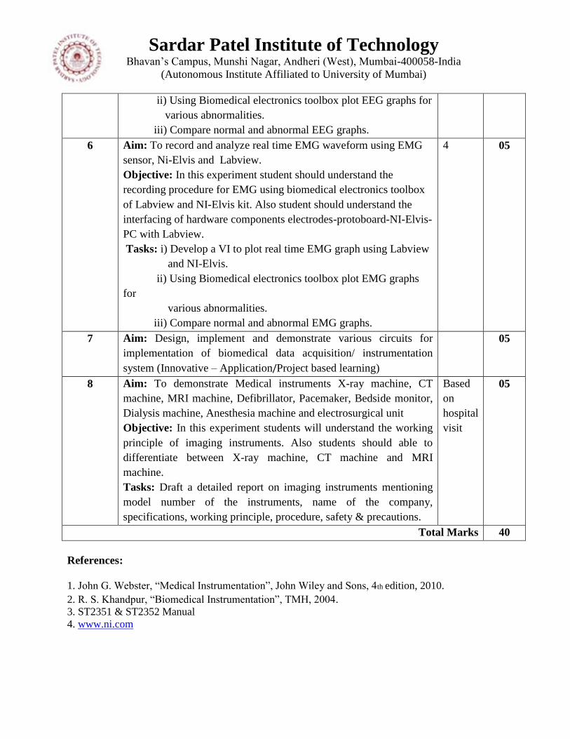
Sardar Patel Institute of Technology Bhavan‟s Campus, Munshi Nagar, Andheri (West), Mumbai-400058-India
(Autonomous Institute Affiliated to University of Mumbai)
ii) Using Biomedical electronics toolbox plot EEG graphs for
various abnormalities.
iii) Compare normal and abnormal EEG graphs.
6 Aim: To record and analyze real time EMG waveform using EMG
sensor, Ni-Elvis and Labview.
Objective: In this experiment student should understand the
recording procedure for EMG using biomedical electronics toolbox
of Labview and NI-Elvis kit. Also student should understand the
interfacing of hardware components electrodes-protoboard-NI-Elvis-
PC with Labview.
Tasks: i) Develop a VI to plot real time EMG graph using Labview
and NI-Elvis.
ii) Using Biomedical electronics toolbox plot EMG graphs
for
various abnormalities.
iii) Compare normal and abnormal EMG graphs.
4 05
7 Aim: Design, implement and demonstrate various circuits for
implementation of biomedical data acquisition/ instrumentation
system (Innovative – Application/Project based learning)
05
8 Aim: To demonstrate Medical instruments X-ray machine, CT
machine, MRI machine, Defibrillator, Pacemaker, Bedside monitor,
Dialysis machine, Anesthesia machine and electrosurgical unit
Objective: In this experiment students will understand the working
principle of imaging instruments. Also students should able to
differentiate between X-ray machine, CT machine and MRI
machine.
Tasks: Draft a detailed report on imaging instruments mentioning
model number of the instruments, name of the company,
specifications, working principle, procedure, safety & precautions.
Based
on
hospital
visit
05
Total Marks 40
References:
1. John G. Webster, “Medical Instrumentation”, John Wiley and Sons, 4th edition, 2010.
2. R. S. Khandpur, “Biomedical Instrumentation”, TMH, 2004.
3. ST2351 & ST2352 Manual
4. www.ni.com


![[16] [4] of RADAR. Vidyalankarvidyalankar.org/file/diploma/Classroom_semVI/ETRX/ACS_Soln.pdf · Vidyalankar : T.Y. Diploma ACS 2 [2 marks] The fusion splicing of single fiber involves](https://img.pdfslide.us/doc/110x75/5e7cef07b767677f066c8dd3/16-4-of-radar-vi-vidyalankar-ty-diploma-acs-2-2-marks-the-fusion-splicing.jpg)


![T.E. Sem. V [ETRX] Linear Integrated Circuit and Design Prelim …vidyalankar.org/file/engg_degree/prelim_paper_soln/SemV/ETRX/LIC.pdf · Linear Integrated Circuit and Design Prelim](https://img.pdfslide.us/doc/110x75/5a8acd327f8b9abb068c048f/te-sem-v-etrx-linear-integrated-circuit-and-design-prelim-integrated-circuit.jpg)