Embed Size (px)
Citation preview
1. Product profile
1.1 General description
The BGU7051 is a low noise high linearity amplifier for wireless infrastructure applications.The LNA has a high input and output return loss and is designed to operate between 0.5 GHz and 1.5 GHz. It is housed in a 3 3 0.85 mm3 10-terminal plastic thin small outline package. The LNA is ESD protected on all terminals.
1.2 Features and benefits
Low Noise Figure (NF) = 0.65 dB at 900 MHz
High linearity performance, IP3O = 33 dBm at 900 MHz
High input and output return loss
Unconditionally stable
110 GHz transit frequency - SiGe:C technology
Supply voltage 3.3 V
Small 10-terminal leadless package 3 3 0.85 mm3
ESD protection on all terminals
Moisture sensitivity level 1
1.3 Applications
LNA for wireless infrastructure applications (0.5 GHz to 1.5 GHz)
Low noise applications
1.4 Quick reference data
BGU7051SiGe:C low noise high linearity amplifierRev. 2 — 11 November 2011 Product data sheet
Table 1. Quick reference dataf = 900 MHz; VCC = 3.3 V; Tamb = 25 C; input and output 50 ; unless otherwise specified.
Symbol Parameter Conditions Min Typ Max Unit
VCC supply voltage 3.0 - 3.6 V
ICC supply current 50 65 80 mA
Gass associated gain 19.5 21.0 22.5 dB
NF noise figure - 0.65 0.95 dB
PL(1dB) output power at 1 dB gain compression 15 16.5 - dBm
IP3O output third-order intercept point 30 33 - dBm
NXP Semiconductors BGU7051SiGe:C low noise high linearity amplifier
2. Pinning information
2.1 Pinning
2.2 Pin description
3. Ordering information
Fig 1. Pin configuration
aaa-000469
BGU7051
GND
RF_IN
GND
RF_OUT
GND GND
VCC1 VCC2
n.c. n.c.
Transparent top view
5 6
4 7
3 8
2 9
1 10
terminal 1index area
Table 2. Pin description
Symbol Pin Description
n.c. 1, 10 not connected
VCC1 2 supply voltage
GND 3, 5, 6, 8 ground
RF_IN 4 RF input
RF_OUT 7 RF output
VCC2 9 supply voltage
Table 3. Ordering information
Type number Package
Name Description Version
BGU7051 HVSON10 plastic thermal enhanced very thin small outline package; no leads; 10 terminals; body 3 3 0.85 mm
SOT650-1
BGU7051 All information provided in this document is subject to legal disclaimers. © NXP B.V. 2011. All rights reserved.
Product data sheet Rev. 2 — 11 November 2011 2 of 13

NXP Semiconductors BGU7051SiGe:C low noise high linearity amplifier
4. Limiting values
5. Thermal characteristics
6. Characteristics
Table 4. Limiting valuesIn accordance with the Absolute Maximum Rating System (IEC 60134).
Symbol Parameter Conditions Min Max Unit
VCC supply voltage 0 5 V
Pi(RF)CW continuous waveform RF input power
VCC = 3.3 V - 20 dBm
Tstg storage temperature 65 150 C
Tj junction temperature - 150 C
Tamb ambient temperature 40 85 C
VESD electrostatic discharge voltage
Human Body Model (HBM); According JEDEC standard 22-A114E
- 4 kV
Charged Device Model (CDM); According JEDEC standard 22-C101B
- 2 kV
Table 5. Thermal characteristics
Symbol Parameter Conditions Typ Unit
Rth(j-sp) thermal resistance from junction to solder point 26 K/W
Table 6. CharacteristicsVCC = 3.3 V; Tamb = 25 C; input and output 50 ; unless otherwise specified. All RF parameters are measured at the device RF in and RF output terminals.
Symbol Parameter Conditions Min Typ Max Unit
VCC supply voltage 3.0 - 3.6 V
ICC supply current 50 65 80 mA
Gass associated gain f = 750 MHz - 23.5 - dB
f = 850 MHz - 21.5 - dB
f = 900 MHz 19.5 21.0 22.5 dB
NF noise figure f = 750 MHz - 0.6 - dB
f = 850 MHz - 0.63 - dB
f = 900 MHz - 0.65 0.95 dB
PL(1dB) output power at 1 dB gain compression f = 750 MHz - 17.0 - dBm
f = 850 MHz - 16.5 - dBm
f = 900 MHz 15 16.5 - dBm
IP3O output third-order intercept point 2-tone; spacing 5 MHz; Pi = 20 dBm
f = 750 MHz - 32 - dBm
f = 850 MHz - 32 - dBm
f = 900 MHz 30 33 - dBm
BGU7051 All information provided in this document is subject to legal disclaimers. © NXP B.V. 2011. All rights reserved.
Product data sheet Rev. 2 — 11 November 2011 3 of 13
NXP Semiconductors BGU7051SiGe:C low noise high linearity amplifier
6.1 Performance curves
RLin input return loss f = 750 MHz - 27.5 - dB
f = 850 MHz - 26.0 - dB
f = 900 MHz - 24.5 - dB
RLout output return loss f = 750 MHz - 18.0 - dB
f = 850 MHz - 17.5 - dB
f = 900 MHz - 18 - dB
ISL isolation f = 750 MHz - 29.5 - dB
f = 850 MHz - 27.5 - dB
f = 900 MHz - 26.5 - dB
K Rollett stability factor 0 GHz f 25 GHz 1 - -
Table 6. Characteristics …continuedVCC = 3.3 V; Tamb = 25 C; input and output 50 ; unless otherwise specified. All RF parameters are measured at the device RF in and RF output terminals.
Symbol Parameter Conditions Min Typ Max Unit
VCC = 3.3 V.
(1) Tj = 40 C
(2) Tj = 25 C
(3) Tj = 85 C
VCC = 3.3 V.
(1) Tj = 40 C
(2) Tj = 25 C
(3) Tj = 85 C
Fig 2. Input reflection coefficient as a function of frequency
Fig 3. Forward transmission coefficient as a function of frequency
f (MHz)500 15001300900 1100700
aaa-000470
-20
-30
-10
0
S11(dB)
-40
(1) (2) (3)
f (MHz)500 15001300900 1100700
aaa-00047135
S21(dB)
25
15
5
0
10
20
30
(1) (3)(2)
BGU7051 All information provided in this document is subject to legal disclaimers. © NXP B.V. 2011. All rights reserved.
Product data sheet Rev. 2 — 11 November 2011 4 of 13
NXP Semiconductors BGU7051SiGe:C low noise high linearity amplifier
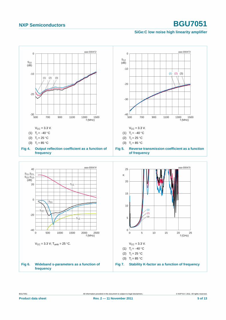
VCC = 3.3 V.
(1) Tj = 40 C
(2) Tj = 25 C
(3) Tj = 85 C
VCC = 3.3 V.
(1) Tj = 40 C
(2) Tj = 25 C
(3) Tj = 85 C
Fig 4. Output reflection coefficient as a function of frequency
Fig 5. Reverse transmission coefficient as a function of frequency
f (MHz)500 15001300900 1100700
aaa-000472
-20
-10
0
S22(dB)
-30
(1) (3)(2)
f (MHz)500 15001300900 1100700
aaa-000473
-20
-30
-10
0
S12(dB)
-40
(1) (3)(2)
VCC = 3.3 V; Tamb = 25 C. VCC = 3.3 V.
(1) Tj = 40 C
(2) Tj = 25 C
(3) Tj = 85 C
Fig 6. Wideband s-parameters as a function of frequency
Fig 7. Stability K-factor as a function of frequency
f (MHz)0 250020001000 1500500
aaa-000474
0
-20
20
40
S11,S21,S22,S12,
(dB)
-40
S21
S22
S11
S12
f (GHz)0 252010 155
aaa-000475
10
15
5
20
25
K
0
(1)(2)(3)
BGU7051 All information provided in this document is subject to legal disclaimers. © NXP B.V. 2011. All rights reserved.
Product data sheet Rev. 2 — 11 November 2011 5 of 13
NXP Semiconductors BGU7051SiGe:C low noise high linearity amplifier
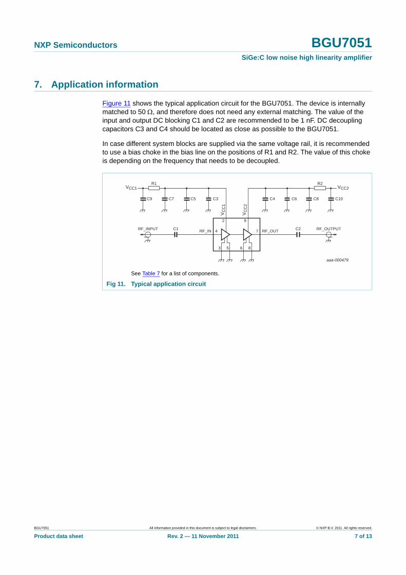
VCC = 3.3 V.
(1) Tj = 40 C
(2) Tj = 25 C
(3) Tj = 85 C
VCC = 3.3 V.
(1) Tj = 40 C
(2) Tj = 25 C
(3) Tj = 85 C
Fig 8. Output power at 1 dB gain compression as a function of frequency
Fig 9. Output third-order intercept point as a function of frequency
aaa-000476
f (MHz)700 1000900800
14
16
12
18
20
PL(1dB)(dBm)
10
(1)(3)(2)
aaa-000477
f (MHz)700 1000900800
20
10
30
40
IP3O(dBm)
0
(1)
(2)(3)
VCC = 3.3 V.
(1) Tj = 40 C
(2) Tj = 25 C
(3) Tj = 85 C
Fig 10. Noise figure as function of frequency
f (MHz)500 15001300900 1100700
aaa-000478
1
0.5
1.5
2
NF(dB)
0
(3)
(1)
(2)
BGU7051 All information provided in this document is subject to legal disclaimers. © NXP B.V. 2011. All rights reserved.
Product data sheet Rev. 2 — 11 November 2011 6 of 13
NXP Semiconductors BGU7051SiGe:C low noise high linearity amplifier
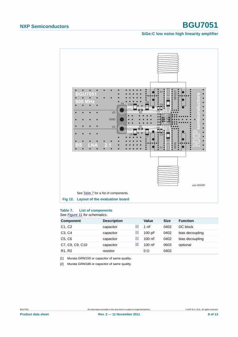
7. Application information
Figure 11 shows the typical application circuit for the BGU7051. The device is internally matched to 50 , and therefore does not need any external matching. The value of the input and output DC blocking C1 and C2 are recommended to be 1 nF. DC decoupling capacitors C3 and C4 should be located as close as possible to the BGU7051.
In case different system blocks are supplied via the same voltage rail, it is recommended to use a bias choke in the bias line on the positions of R1 and R2. The value of this choke is depending on the frequency that needs to be decoupled.
See Table 7 for a list of components.
Fig 11. Typical application circuit
VC
C1
VCC1 VCC2
VC
C2
C1
C9
R1 R2
C7 C5 C3 C4 C6 C8 C10
RF_INPUT C2 RF_OUTPUTRF_IN
3 5 6 8
74
2 9
RF_OUT
aaa-000479
BGU7051 All information provided in this document is subject to legal disclaimers. © NXP B.V. 2011. All rights reserved.
Product data sheet Rev. 2 — 11 November 2011 7 of 13
NXP Semiconductors BGU7051SiGe:C low noise high linearity amplifier
[1] Murata GRM155 or capacitor of same quality.
[2] Murata GRM188 or capacitor of same quality.
See Table 7 for a list of components.
Fig 12. Layout of the evaluation board
Table 7. List of componentsSee Figure 11 for schematics.
Component Description Value Size Function
C1, C2 capacitor [1] 1 nF 0402 DC block
C3, C4 capacitor [1] 100 pF 0402 bias decoupling
C5, C6 capacitor [1] 100 nF 0402 bias decoupling
C7, C8, C9, C10 capacitor [2] 100 nF 0603 optional
R1, R2 resistor 0 0402
aaa-000480
C10
C9C7
X3 C8
C5
C6
C4
X2
GND
V2
V1
X1 RFI
NR
FOU
T
C3
C2
C1
R2
R1
BGU7051 All information provided in this document is subject to legal disclaimers. © NXP B.V. 2011. All rights reserved.
Product data sheet Rev. 2 — 11 November 2011 8 of 13
NXP Semiconductors BGU7051SiGe:C low noise high linearity amplifier
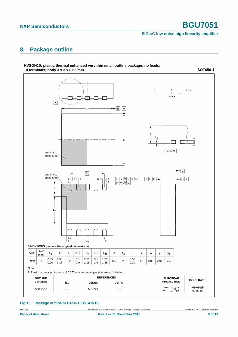
8. Package outline
Fig 13. Package outline SOT650-1 (HVSON10)
0.50.210.050.00
A1 EhbUNIT D(1) ye
2
e1
REFERENCESOUTLINEVERSION
EUROPEANPROJECTION ISSUE DATE
IEC JEDEC JEITA
mm 3.12.9
c Dh
1.751.45
y1
3.12.9
2.552.15
0.300.18
0.05 0.1
DIMENSIONS (mm are the original dimensions)
SOT650-1 MO-229 - - -- - -
E(1)
0.550.30
L
0.1
v
0.05
w
0 2 mm1
scale
SOT650-1HVSON10: plastic thermal enhanced very thin small outline package; no leads;10 terminals; body 3 x 3 x 0.85 mm
A(1)
max.
AA1
c
detail X
y
Dh
Eh
e
L
10
51
6
D
E
y1 C
C
B A
01-01-2202-02-08
terminal 1index area
terminal 1index area
X
e1
b ACC
Bv M
w M
Note
1. Plastic or metal protrusions of 0.075 mm maximum per side are not included.
BGU7051 All information provided in this document is subject to legal disclaimers. © NXP B.V. 2011. All rights reserved.
Product data sheet Rev. 2 — 11 November 2011 9 of 13

NXP Semiconductors BGU7051SiGe:C low noise high linearity amplifier
9. Abbreviations
10. Revision history
Table 8. Abbreviations
Acronym Description
AC Alternating Current
CW Continuous Wave
ESD ElectroStatic Discharge
ESR Equivalent Series Resistance
HBM Human Body Model
LNA Low Noise Amplifier
PDA Personal Digital Assistant
RF Radio Frequency
SiGe:C Silicon Germanium Carbon
Table 9. Revision history
Document ID Release date Data sheet status Change notice Supersedes
BGU7051 v.2 20111111 Product data sheet - BGU7051 v.1
Modifications: • Figure 10: data plots updated
• Unit dB changed to dBm for PL(1dB) in Section 6 “Characteristics”
BGU7051 v.1 20111027 Product data sheet - -
BGU7051 All information provided in this document is subject to legal disclaimers. © NXP B.V. 2011. All rights reserved.
Product data sheet Rev. 2 — 11 November 2011 10 of 13
NXP Semiconductors BGU7051SiGe:C low noise high linearity amplifier
11. Legal information
11.1 Data sheet status
[1] Please consult the most recently issued document before initiating or completing a design.
[2] The term ‘short data sheet’ is explained in section “Definitions”.
[3] The product status of device(s) described in this document may have changed since this document was published and may differ in case of multiple devices. The latest product status information is available on the Internet at URL http://www.nxp.com.
11.2 Definitions
Draft — The document is a draft version only. The content is still under internal review and subject to formal approval, which may result in modifications or additions. NXP Semiconductors does not give any representations or warranties as to the accuracy or completeness of information included herein and shall have no liability for the consequences of use of such information.
Short data sheet — A short data sheet is an extract from a full data sheet with the same product type number(s) and title. A short data sheet is intended for quick reference only and should not be relied upon to contain detailed and full information. For detailed and full information see the relevant full data sheet, which is available on request via the local NXP Semiconductors sales office. In case of any inconsistency or conflict with the short data sheet, the full data sheet shall prevail.
Product specification — The information and data provided in a Product data sheet shall define the specification of the product as agreed between NXP Semiconductors and its customer, unless NXP Semiconductors and customer have explicitly agreed otherwise in writing. In no event however, shall an agreement be valid in which the NXP Semiconductors product is deemed to offer functions and qualities beyond those described in the Product data sheet.
11.3 Disclaimers
Limited warranty and liability — Information in this document is believed to be accurate and reliable. However, NXP Semiconductors does not give any representations or warranties, expressed or implied, as to the accuracy or completeness of such information and shall have no liability for the consequences of use of such information.
In no event shall NXP Semiconductors be liable for any indirect, incidental, punitive, special or consequential damages (including - without limitation - lost profits, lost savings, business interruption, costs related to the removal or replacement of any products or rework charges) whether or not such damages are based on tort (including negligence), warranty, breach of contract or any other legal theory.
Notwithstanding any damages that customer might incur for any reason whatsoever, NXP Semiconductors’ aggregate and cumulative liability towards customer for the products described herein shall be limited in accordance with the Terms and conditions of commercial sale of NXP Semiconductors.
Right to make changes — NXP Semiconductors reserves the right to make changes to information published in this document, including without limitation specifications and product descriptions, at any time and without notice. This document supersedes and replaces all information supplied prior to the publication hereof.
Suitability for use — NXP Semiconductors products are not designed, authorized or warranted to be suitable for use in life support, life-critical or safety-critical systems or equipment, nor in applications where failure or
malfunction of an NXP Semiconductors product can reasonably be expected to result in personal injury, death or severe property or environmental damage. NXP Semiconductors accepts no liability for inclusion and/or use of NXP Semiconductors products in such equipment or applications and therefore such inclusion and/or use is at the customer’s own risk.
Applications — Applications that are described herein for any of these products are for illustrative purposes only. NXP Semiconductors makes no representation or warranty that such applications will be suitable for the specified use without further testing or modification.
Customers are responsible for the design and operation of their applications and products using NXP Semiconductors products, and NXP Semiconductors accepts no liability for any assistance with applications or customer product design. It is customer’s sole responsibility to determine whether the NXP Semiconductors product is suitable and fit for the customer’s applications and products planned, as well as for the planned application and use of customer’s third party customer(s). Customers should provide appropriate design and operating safeguards to minimize the risks associated with their applications and products.
NXP Semiconductors does not accept any liability related to any default, damage, costs or problem which is based on any weakness or default in the customer’s applications or products, or the application or use by customer’s third party customer(s). Customer is responsible for doing all necessary testing for the customer’s applications and products using NXP Semiconductors products in order to avoid a default of the applications and the products or of the application or use by customer’s third party customer(s). NXP does not accept any liability in this respect.
Limiting values — Stress above one or more limiting values (as defined in the Absolute Maximum Ratings System of IEC 60134) will cause permanent damage to the device. Limiting values are stress ratings only and (proper) operation of the device at these or any other conditions above those given in the Recommended operating conditions section (if present) or the Characteristics sections of this document is not warranted. Constant or repeated exposure to limiting values will permanently and irreversibly affect the quality and reliability of the device.
Terms and conditions of commercial sale — NXP Semiconductors products are sold subject to the general terms and conditions of commercial sale, as published at http://www.nxp.com/profile/terms, unless otherwise agreed in a valid written individual agreement. In case an individual agreement is concluded only the terms and conditions of the respective agreement shall apply. NXP Semiconductors hereby expressly objects to applying the customer’s general terms and conditions with regard to the purchase of NXP Semiconductors products by customer.
No offer to sell or license — Nothing in this document may be interpreted or construed as an offer to sell products that is open for acceptance or the grant, conveyance or implication of any license under any copyrights, patents or other industrial or intellectual property rights.
Export control — This document as well as the item(s) described herein may be subject to export control regulations. Export might require a prior authorization from competent authorities.
Document status[1][2] Product status[3] Definition
Objective [short] data sheet Development This document contains data from the objective specification for product development.
Preliminary [short] data sheet Qualification This document contains data from the preliminary specification.
Product [short] data sheet Production This document contains the product specification.
BGU7051 All information provided in this document is subject to legal disclaimers. © NXP B.V. 2011. All rights reserved.
Product data sheet Rev. 2 — 11 November 2011 11 of 13
NXP Semiconductors BGU7051SiGe:C low noise high linearity amplifier
Non-automotive qualified products — Unless this data sheet expressly states that this specific NXP Semiconductors product is automotive qualified, the product is not suitable for automotive use. It is neither qualified nor tested in accordance with automotive testing or application requirements. NXP Semiconductors accepts no liability for inclusion and/or use of non-automotive qualified products in automotive equipment or applications.
In the event that customer uses the product for design-in and use in automotive applications to automotive specifications and standards, customer (a) shall use the product without NXP Semiconductors’ warranty of the product for such automotive applications, use and specifications, and (b) whenever customer uses the product for automotive applications beyond NXP Semiconductors’ specifications such use shall be solely at customer’s own risk, and (c) customer fully indemnifies NXP Semiconductors for any
liability, damages or failed product claims resulting from customer design and use of the product for automotive applications beyond NXP Semiconductors’ standard warranty and NXP Semiconductors’ product specifications.
Quick reference data — The Quick reference data is an extract of the product data given in the Limiting values and Characteristics sections of this document, and as such is not complete, exhaustive or legally binding.
11.4 TrademarksNotice: All referenced brands, product names, service names and trademarks are the property of their respective owners.
12. Contact information
For more information, please visit: http://www.nxp.com
For sales office addresses, please send an email to: [email protected]
BGU7051 All information provided in this document is subject to legal disclaimers. © NXP B.V. 2011. All rights reserved.
Product data sheet Rev. 2 — 11 November 2011 12 of 13
NXP Semiconductors BGU7051SiGe:C low noise high linearity amplifier
13. Contents
1 Product profile . . . . . . . . . . . . . . . . . . . . . . . . . . 11.1 General description . . . . . . . . . . . . . . . . . . . . . 11.2 Features and benefits . . . . . . . . . . . . . . . . . . . . 11.3 Applications . . . . . . . . . . . . . . . . . . . . . . . . . . . 11.4 Quick reference data . . . . . . . . . . . . . . . . . . . . 1
2 Pinning information. . . . . . . . . . . . . . . . . . . . . . 22.1 Pinning . . . . . . . . . . . . . . . . . . . . . . . . . . . . . . . 22.2 Pin description . . . . . . . . . . . . . . . . . . . . . . . . . 2
3 Ordering information. . . . . . . . . . . . . . . . . . . . . 2
4 Limiting values. . . . . . . . . . . . . . . . . . . . . . . . . . 3
5 Thermal characteristics . . . . . . . . . . . . . . . . . . 3
6 Characteristics. . . . . . . . . . . . . . . . . . . . . . . . . . 36.1 Performance curves . . . . . . . . . . . . . . . . . . . . . 4
7 Application information. . . . . . . . . . . . . . . . . . . 7
8 Package outline . . . . . . . . . . . . . . . . . . . . . . . . . 9
9 Abbreviations. . . . . . . . . . . . . . . . . . . . . . . . . . 10
10 Revision history. . . . . . . . . . . . . . . . . . . . . . . . 10
11 Legal information. . . . . . . . . . . . . . . . . . . . . . . 1111.1 Data sheet status . . . . . . . . . . . . . . . . . . . . . . 1111.2 Definitions. . . . . . . . . . . . . . . . . . . . . . . . . . . . 1111.3 Disclaimers . . . . . . . . . . . . . . . . . . . . . . . . . . . 1111.4 Trademarks. . . . . . . . . . . . . . . . . . . . . . . . . . . 12
12 Contact information. . . . . . . . . . . . . . . . . . . . . 12
13 Contents . . . . . . . . . . . . . . . . . . . . . . . . . . . . . . 13
© NXP B.V. 2011. All rights reserved.
For more information, please visit: http://www.nxp.comFor sales office addresses, please send an email to: [email protected]
Date of release: 11 November 2011
Document identifier: BGU7051
Please be aware that important notices concerning this document and the product(s)described herein, have been included in section ‘Legal information’.