Embed Size (px)
Citation preview

BGA242: TD242LP Evaluation Board User’s Guide
TransDimension Inc. 135 Technology Drive
Irvine, CA 92618 http://www.transdimension.com
Phone: 949-727-2020 Fax: 949-727-3232
[email protected] [email protected]
TDI Document Number: MU4006
Rev. 2.1: July 2005

TransDimension Inc. BGA242:TD242LP Evaluation Board User’s Guide
TransDimension Inc. – Proprietary
THE DEVICE AND ITS DOCUMENTATION ARE PROVIDED “AS IS”. TRANSDIMENSION HEREBY DISCLAIMS ALL WARRANTIES, EXPRESS, STATUTORY AND IMPLIED, APPLICABLE TO THE SOFTWARE AND ITS DOCUMENTATION AND ANY RELATED PRODUCTS, INCLUDING, BUT NOT LIMITED TO, ANY WARRANTY OF MERCHANTABILITY, NON-INFRINGEMENT OR FITNESS FOR A PARTICULAR PURPOSE. TRANSDIMENSION ASSUMES NO LIABILITY FOR ANY ACT OR OMISSION OF LICENSEE. IN NO EVENT SHALL TRANSDIMENSION BE LIABLE FOR DIRECT, SPECIAL, INDIRECT, INCIDENTAL, PUNITIVE, EXEMPLARY OR CONSEQUENTIAL DAMAGES, INCLUDING, WITHOUT LIMITATION, LOSS OF PROFITS OR REVENUE, LOSS OF PRODUCTS, DATA OR ANY ASSOCIATED EQUIPMENT, COST OF CAPITAL, COST OF SUBSTITUTED EQUIPMENT OR PARTS, FACILITIES OR SERVICES, DOWN-TIME OR LABOR COSTS, EVEN IF TRANSDIMENSION HAS BEEN ADVISED OF THE POSSIBILITY THEREOF. The device and any related products are not designed, authorized, or warranted to be suitable for use in life-support devices or systems or other critical applications. Any such use and subsequent liabilities that may arise from such use are totally the responsibilities of the Licensee. All product names are trademarks or registered trademarks of their respective owners. © 2005, TransDimension Inc., All rights reserved. .

TransDimension Inc. BGA242: TD242LP Evaluation Board User’s Guide
TransDimension Inc. – Proprietary 1
Revision History
Version Release Date Author Note 0.1 2/13/2003 J Roeder Draft 1.0 4/17/2003 J Fung First release 1.1 4/20/2003 J Fung Added QFP schematic, notation 2.0 12/10/03 J Roeder Name change to TD242LP.
VBUS schematic changes. 2.1 7/21/2005 J Roeder Changed pin B2 of the BGA package
symbol in the schematics to AVDD2.5 from VDD2.5
Note: This document is subject to change without notice.

TransDimension Inc. BGA242: TD242LP Evaluation Board User’s Guide
TransDimension Inc. – Proprietary 2
Contents
1 TD242LP: USB OTG Host/Function Controller ....................................................................3 1.1 Pin Assignments...................................................................................................5
2 Microprocessor Interface ........................................................................................................6
3 BGA242 Evaluation Board .....................................................................................................7 3.1 General Description .............................................................................................7 3.2 Board Operation Requirements............................................................................9
4 Hardware Description/Configuration......................................................................................9 4.1 Default Factory Settings – Standalone Configuration (BGA242S).....................9 4.2 Optional Configuration Installations....................................................................9 4.3 TD242LP Reset..................................................................................................10 4.4 DP/DM Signals ..................................................................................................10 4.5 LEDs ..................................................................................................................10 4.6 Oscillator Input ..................................................................................................10 4.7 Mounting Holes .................................................................................................10
5 Power Supply ........................................................................................................................10 5.1 5V Power Supply ...............................................................................................11 5.2 3.3V Power Supply ............................................................................................11 5.3 2.5V Core Power Supply ...................................................................................11 5.4 3.3V/2.5V Wide Range I/O Power Supply........................................................11
6 Test Points.............................................................................................................................11
7 References.............................................................................................................................12
8 Schematic..............................................................................................................................12 BGA242: Top Level ....................................................................................................13 BGA242: Test Headers ................................................................................................14 BGA242: TD242LP.....................................................................................................15 BGA242: PC104 Connectors.......................................................................................16 BGA242: Power Distribution ......................................................................................17 BGA242: System CPLD..............................................................................................18 BGA242: USB Ports ....................................................................................................19

TransDimension Inc. BGA242: TD242LP Evaluation Board User’s Guide
TransDimension Inc. – Proprietary 3
Voltage Regulator
PLL OSC2 CLKW/ CLKCFG
OSC1 48 MHz 12 MHz
/RESET
/CS /WR /RD
A12:A1 D15:D0
INT
TEST
Memory Blocks
OTG Trans- ceiver
Host SIE &
Root Hub
µP Interface
USB Host Controller Registers
System Configuration
& Control
Registers
USB Function Controller Registers
USB Host
Control Logic
Function SIE
USB Trans- ceiver
DM2 DP2
DM1 DP1
/PO /OC
VBus Control Circuit
HNP/ SRP Logic ID
Test Control
ENVREG VREGOUT VBUS /EXVBO
PSH
USB Function Control Logic
H/F
PSFPSH
PSC
VBP
1 TD242LP: USB OTG Host/Function Controller TransDimension’s TD242LP (TDI part number: TDOTG242-000C 64 pin LQFP, and TDOTG242-00BC for 64 pin BGA) is the second controller in the family of integrated low-cost, high-performance, On-the-Go (OTG) controllers. The TD242LP is a combination of a standard USB host controller and an OTG dual-role device controller. Designed specifically for embedded applications with a non-PCI microprocessor interface, this 16-bit interface is ideal for low power mobile applications. It is USB Specification 2.0 compliant, operating at full speed (12Mb/s) and/or low speed (1.5Mb/s). The controller supports all four types of USB transfers: Control, Interrupt, Bulk, and Isochronous with highest data throughput, and lowest interrupt rate among all embedded host controllers on the market. In particular, isochronous performance is guaranteed. The pipe/transfer level programming makes the TD242LP very easy to use, ensuring shortest time-to-market. The block diagram of the TD242LP is shown in Figure 1-1. The TD242LP operational modes are given in Figure 1-2.
Figure 1-1: TD242LP OTG Host/Function Controller

TransDimension Inc. BGA242: TD242LP Evaluation Board User’s Guide
TransDimension Inc. – Proprietary 4
The TD242LP chip can be configured by software to operate in any of four modes as described in Figure 1-2. Description Hardware HNP
• State machines for both the A-DEVICE and B-DEVICE are updated and tracked by the Hardware. • All timers are started and stopped by the Hardware events. • The OTG port can work either as a USB Host or USB Function, as determined by the automatic
negotiation with the connected remote device. Host Only Mode
• All the ports are USB Hosts. The HNP and Function are disabled. Function Host Mode
• The dual-role USB port operates as a USB Function. The other port will operate as USB Host. The HNP is disabled in this mode.
Software HNP • The TD242LP will allow Software to control the operation of the shared USB port. Software is
responsible for the timing, control of the external charge pump, tracking the HNP state and performing the HNP protocol.
• The shared OTG port can work either as a USB Host or USB Function, as determined by the Software negotiation with the connected remote device. Note: Software HNP is quite CPU intensive.
Figure 1-2: TD242LP Operating modes
The TD242LP is targeted towards embedded applications with low power requirements, especially mobile and post-PC products, including cellular phones, palm platforms, PDAs, STBs, home gateway systems, and Internet appliances. Peer-to-Peer communication is made simple with the TD242LP as USB connectivity is achieved without PC intervention. TransDimension, together with SoftConnex Inc, a wholly owned subsidiary, offer total solutions including controller chips, reference designs and development kits, firmware for microprocessor interfacing, HCD (Host Controller Driver), HNP (Host Negotiation Protocol), SRP (Session Request Protocol) as well as USB host and function stacks running under most real time operating systems.
TransDimension Inc. BGA242: TD242LP Evaluation Board User’s Guide
TransDimension Inc. – Proprietary 5
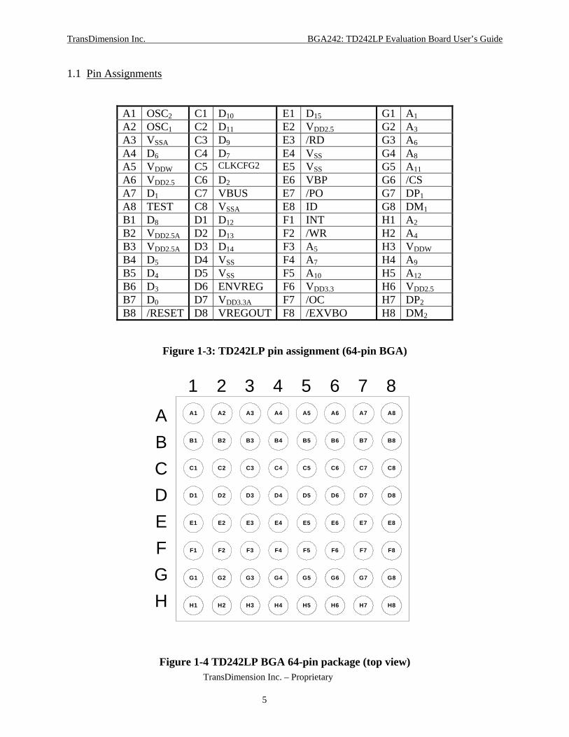
1.1 Pin Assignments
A1 OSC2 C1 D10 E1 D15 G1 A1 A2 OSC1 C2 D11 E2 VDD2.5 G2 A3 A3 VSSA C3 D9 E3 /RD G3 A6 A4 D6 C4 D7 E4 VSS G4 A8 A5 VDDW C5 CLKCFG2 E5 VSS G5 A11 A6 VDD2.5 C6 D2 E6 VBP G6 /CS A7 D1 C7 VBUS E7 /PO G7 DP1 A8 TEST C8 VSSA E8 ID G8 DM1 B1 D8 D1 D12 F1 INT H1 A2 B2 VDD2.5A D2 D13 F2 /WR H2 A4 B3 VDD2.5A D3 D14 F3 A5 H3 VDDW B4 D5 D4 VSS F4 A7 H4 A9 B5 D4 D5 VSS F5 A10 H5 A12 B6 D3 D6 ENVREG F6 VDD3.3 H6 VDD2.5 B7 D0 D7 VDD3.3A F7 /OC H7 DP2 B8 /RESET D8 VREGOUT F8 /EXVBO H8 DM2
Figure 1-3: TD242LP pin assignment (64-pin BGA)
Figure 1-4 TD242LP BGA 64-pin package (top view)
TDOTG242
A1
B1
C1
D1
E1
F1
G1
H1
A2
B2
C2
D2
E2
F2
G2
H2
A3
B3
C3
D3
E3
F3
G3
H3
A4
B4
C4
D4
E4
F4
G4
H4
A5
B5
C5
D5
E5
F5
G5
H5
A6
B6
C6
D6
E6
F6
G6
H6
A7
B7
C7
D7
E7
F7
G7
H7
A8
B8
C8
D8
E8
F8
G8
H8
ABCDEFGH
1 2 3 4 5 6 7 8

TransDimension Inc. BGA242: TD242LP Evaluation Board User’s Guide
TransDimension Inc. – Proprietary 6
TDOTG242LP
Figure 1-5 TD242LP BGA 64-pin package (top view) 2 Microprocessor Interface The TD242LP supports a 16-bit interface whether it be a microcontroller, a microprocessor, or a custom ASIC. Figure 2-1 shows a typical interface between the TD242LP and a microprocessor.
8 7 6 5 4 3 2 1
A B C D E F G H

TransDimension Inc. BGA242: TD242LP Evaluation Board User’s Guide
TransDimension Inc. – Proprietary 7
Figure 2-1: A typical TD242LP interface to a microprocessor
3 BGA242 Evaluation Board 3.1 General Description The BGA242 (TDI part number TDOTG242-1010) evaluation board is designed for internal software development and customer evaluation of the TD242LP chip. Measured at 4.80 in. (121.9mm) by 3.00 in. (76.2mm), it can be employed to:
• Evaluate TransDimension's TD242LP USB OTG Host/Function Controller; • Run TD242LP demonstrations; • Develop user software for TD242LP based applications; and • Serve as a subassembly in an OEM's product to provide USB OTG Host/Function
Controller. With the block diagram of Figure 2-1, the BGA242 has the following features:
• Onboard TD242LP chip (64-pin, BGA package). • Onboard USB power distribution and over-current protection circuit for host applications. • One mini-AB OTG port and one Type A USB port.
/RESET
TEST
16
OSC1 OSC2
Crystal (Oscillator)
Circuit
GPIOR
A12:A1 D15:D0
12
/CS /WR/RD
INT /INTP
/CSK /WR /RD
A12:A1 D15:D0
Microprocessor
10K
3.3V
3.3V
10K x 4

TransDimension Inc. BGA242: TD242LP Evaluation Board User’s Guide
TransDimension Inc. – Proprietary 8
• Onboard Dual footprint USB mini-AB OTG socket and a Dual footprint USB Type A socket for host operations.
• Onboard 6 MHz crystal. • Onboard test points for key signal probing. • Support for both self-powered and bus powered USB function. • Standard PC104 connector for interface to PC Motherboard or our PCI104 PCI adaptor
card. • 5V supply through the interfacing connector with LEDs indicating power conditions. • Support for both 2.5V and 3.3V I/O’s. • Low powered 2.5V core operating voltage.
5.0V to 3.3V DC Converter
2.5V Core
3.3V
2.5 or 3.3V I/O
PC104
CONNECTOR
5V
Mictor Test Header
(Optional)
5.0V to 2.5V Converter
Resistor
Port 1 Mini AB
Port 2 Type A
Processor Bus TD242LP
BGA64
VREGOUT
Crystal TPS2044
Figure 3-1 EVB242 Block Diagram

TransDimension Inc. BGA242: TD242LP Evaluation Board User’s Guide
TransDimension Inc. – Proprietary 9
3.2 Board Operation Requirements The following items are required to operate the BGA242:
• A DC power source capable of supplying 5V±10%@1.5A through a power switch. Regulated power supply is required.
4 Hardware Description/Configuration The BGA242 was designed for either stand alone use or for use in a PCI bus configuration; the BGA242S for standalone and BGA242P for PCI. The PCE242 evaluation system is a combination of the BGA242P and a PCI104 bridge board. Switching in between the two configurations consists of either installing or removing a couple of resistors and moving a jumper. Please refer to the following check lists to see if you have the correct board configuration. 4.1 Default Factory Settings – Standalone Configuration (BGA242S) The default settings support the development of:
• an OTG Dual Role Device (Port 1) and a USB host (Port 2) simultaneously • a self powered or a bus powered USB function port (Port 1) and a USB Host (Port 2)
simultaneously Please double check the factory settings given below before using the board.
• R1, R13: (0 ohm) populated • R15: (0 ohm) populated • R19: (0 ohm) populated • R41 (10k ohm) populated • R44, R51: (10kohm, 100ohm) populated • R52: (0 ohm) populated • R53: (0 ohm) populated • J3: Pins 7 and 8 jumpered
4.2 Optional Configuration Installations To use the BGA242 as a USB Host on both ports (Port 1 and Port 2), make the following changes:
• R54: Install for Host Controller operation (R53 must be removed) To use different sources for the I/O Voltage supplies, do one of the following:
• R16: Install to use the Internal OTG_VREG for the 2.5V I/O (R15, R17 removed) • R17: Install to use the external 5V-to-2.5V regulator for the 2.5V I/O (R15, R16
removed) AND R42: Install to disable the Internal OTG_VREG (R41 is removed)

TransDimension Inc. BGA242: TD242LP Evaluation Board User’s Guide
TransDimension Inc. – Proprietary 10
To use the external regulator as the 2.5V Core Voltage supplies, do the following:
• R18: Install to use the 5V-to-2.5V regulator for the 2.5V core (R19 removed) NOTE: OTG_VREG is the internal voltage regulator inside the TD242LP chip. The internal OTG_VREG can be disabled by installing R42 (R41 removed) and also removing R16 and R19. 4.3 TD242LP Reset The /RESET of the TD242LP is brought out to the PC104 connector. Users can control the /RESET through a GPIO of the MCU as depicted in Fig. 2-1. 4.4 DP/DM Signals Each of the DP/DM pairs has a 2-pin, 0.1” spacing, connector for attaching a differential probe. These traces are impedance controlled to 90 ohms + 10%. 4.5 LEDs The BGA242 board supplies several LEDs to check the normal operation of the board. These LEDs should be green for the functions that are working correctly: D14: 3.3V Power Rail Indicator D2: 2.5V Power Rail Indicator D3: VDDW Power Rail Indicator D4: 5.0V Power Rail Indicator D1: Type A VBUS Power Indicator D5: Mini-AB VBUS Power Indicator 4.6 Oscillator Input The TD242LP supports the use of a 6MHz crystal, or a crystal oscillator of 6, 12, 24 or 48MHz. The 12 or 24MHz crystal oscillator is supported only for the BGA package. A 6MHz crystal or a 6MHz crystal oscillator is recommended for lower EMI. The only footprint provided in the BGA242 board is the use of a 6MHz (default) crystal. 4.7 Mounting Holes The BGA242 board has four unplated standoff holes, one near each corner of the board. Each hole is 0.146” in diameter. The placement matches the PCI104 PCI board. 5 Power Supply Before using the BGA242, one must determine the way the power is applied to the board. Listed below are the configurations for both the core and I/O voltage supplies. The default

TransDimension Inc. BGA242: TD242LP Evaluation Board User’s Guide
TransDimension Inc. – Proprietary 11
configuration assumes that the user will be using the internal voltage regulator (OTG_VREG) supply for the 2.5V core voltage and the 5V-to-3.3V converter for the 3.3V I/O supply. 5.1 5V Power Supply The BGA242 board will receive its 5V power from one of two sources. The source will be resistor selectable.
1. The PC104 Connector [Default setting]. 2. An external source connecting to a test pin. Protection circuitry is not provided. (remove
R1 and R13) 5.2 3.3V Power Supply The BGA242 board will receive its 3.3V power only from a voltage regulator.
1. The 5V-to-3.3V DC converter. 5.3 2.5V Core Power Supply The BGA242 board will receive its 2.5V core power from one of three sources. The source will be resistor selectable.
1. The TD242LP’s internal regulator output pin, VREGOUT [Default setting]. 2. The 5.0V-to-2.5V DC converter. 3. An external source connecting to a test pin (JP4, pin 3). Protection circuitry is not
provided. The power for the core voltage (VDD2.5 pins) is independent from the power for the I/O voltage, meaning you can drive the core from the internal regulator and drive the 2.5V I/O from the DC converter. 5.4 3.3V/2.5V Wide Range I/O Power Supply The BGA242 board will receive its power from one of three sources. The VDDW (VDD Wide-range) power source will be resistor selectable.
1. From the 3.3V supply directly (3.3V) [Default setting]. 2. The TD242LP’s internal regulator output pin, VREGOUT (2.5V). 3. The 5.0V-to-2.5V DC converter (2.5V). 4. An external source connecting to a test pin (JP3, pin 3). Protection circuitry is not
provided. 6 Test Points The following test points are furnished on the BGA242: Ground Test Points JP1, JP2, JP9 and JP10 VBUS, DP1, DM1, DP2, DM2, VREG_OUT, ID.

TransDimension Inc. BGA242: TD242LP Evaluation Board User’s Guide
TransDimension Inc. – Proprietary 12
7 References • USB 2.0 Specification (www.usb.org) • USB On-The-Go Supplement to USB 2.0 Specification (www.usb.org) • TD242LP Technical Manual (TDI Document Number: MU4006) 8 Schematic The schematics of the BGA242 are presented on Pages 13-19 of this document. NOTE: The TD242LP also comes in an LQFP64 package which is not shown in the schematics.

TransDimension Inc. BGA242: TD242LP Evaluation Board User’s Guide
TransDimension Inc. – Proprietary 13
BGA242: Top Level
PO_N
OTG_CSL
RESET_LOCALL
D[7:0]
A11
D6
GPIO8
A4
A7
D[15:0]
RESET_CONN
CPLD_READYL
A2
TD242LP
TD242LP
OTG_INTL
RESET_CONN
OTG_CSL
OTG_WRLOTG_RDL
OTG_D[15:0]
OTG_A[12:1]
OTG_DP1_ROTG_DM1_R
OTG_DP2_ROTG_DM2_R
OTG_ID
OTG_POLOTG_OCL
OTG_EXVBOL
OTG_VBP
OTG_VREG_OUT
OTG_VBUS
RESET_LOCALL
CPLD_CSL
OTG_WRLOTG_INTL
A19
GPIO7
A[19:0]
OTG_INTL
CPLD_READYL
D7 DP1_R
D5
A16
OTG_RDL
A17
Sy stem_CPLD
Sy stem_PLD
RESET_LOCALLRESET_CONN
OTG_RDLOTG_WRL
CPLD_CSL
OTG_CSLA[19:13]
D[7:0]
OTG_CSL_CONN
CPLD_READYLALEL
GPIO7GPIO8
A[3:0]
OTG_RDL
EXT_VBO_N
A9
OC_N
USB_PORTS
USB_PORTS
DP1_RDM1_R
DP2_RDM2_R
ID
PO_NOC_N
EXT_VBO_N
VBPVBUS
OTG_WRL
D4
A8
D1
A1
VBP
D0
OTG_CSL_CONN
DP2_R
A10
RESET_CONN
OTG_CSL
A0
OTG_INTL
A15
CPLD_CSL
VREG_OUT
ALEL
PC104_CONN
PC104_CONN
RESET
SD[15:0]
SA[19:0]
CS1L
/MEMRD/MEMWR
CS2L
OTG_INTL
READYLBALE
GPIO7GPIO8
GPIO7
GPIO8
A3
A[12:1]
RESET_LOCALL
A14
ALEL
OTG_WRL
A3
A5
A1
D3D2
RESET_CONN
A[19:0]
DM2_R
CPLD_READYL
VBUS
Power_Dist
Power_Dist
VREG_OUT
ALEL
OTG_CSL
OTG_CSL_CONN
A13
DM1_RD[15:0]
A18
GPIO8
A[3:0]
A12
BGA242 CARD TOP LEVEL
A[19:13]
A6
SC-OTG242-A2-001 2.1
BGA242 Card : TOP LEVEL
1 7Thursday , July 21, 2005
Title
Size Document Number Rev
Date: Sheet of
RESET_LOCALL
OTG_RDL
A2
D[15:0]
ID
GPIO7
A[19:0]
CPLD_CSLOTG_CSL_CONN
Rev2.1: 1. TD242LP pin B2 to AVDD2.5 from VDD2.5 2. Removed DNI pulldowns on DP/DM

TransDimension Inc. BGA242: TD242LP Evaluation Board User’s Guide
TransDimension Inc. – Proprietary 14
BGA242: Test Headers
D10
MH's are to be .146" non-plated thru holesPlace one at each corner.
A14
D14
A12
D1
OTG_WRL
A9
A6V241
V261
RESET_CONN
RESET_CONN
TEST HEADERS
OTG_CSL
GPIO8
A1
D7
V20 1
A11
GPIO8
RESET_LOCALL
D5
OTG_CSL
A13
OTG_WRL
MH3
JP9
1X2
21
GROUND TEST POINTS
JP1
1X2
21
V211
A2
D15
V221
RESET_LOCALL
D0
A18
V12 1
Female Mictor ConnectorAMP 2-767004-2AMP 767054-1Emulation Tech CONMICFEM38SMT
A19
OTG_WRL
V19 1
GPIO7
D11
D[15:0]
A17MH2
V18 1
A7
D8
A10
OTG_CSL_CONN
MH1
V16 1
OTG_RDL
V251OTG_INTL
V231
RESET_LOCALL
Distribute the TestPointson top side near corners
GPIO7
MH4
D[15:0]
OTG_CSL
CPLD_CSL
OTG_RDL
ALEL
A4
CPLD_CSL
D[15:0]
A8
A5
CPLD_READYL CPLD_READYL
D13
OTG_RDL
D2
GPIO7
A0
ALEL
V17 1D9
JP2
1X2
21
JP10
1X2
21
A16
A[19:0]
A3
J4Mictor38
135791113151719212325272931333537
2468
101214161820222426283032343638
39 4041 42 43
D3
D12
CPLD_READYL
GPIO8
A15
OTG_INTL
SC-OTG242-A2-002 2.1
BGA242 Card : Headers
2 7Thursday , July 21, 2005
Title
Size Document Number Rev
Date: Sheet of
OTG_CSL_CONN
ALEL
A[19:0]
J5Mictor38
135791113151719212325272931333537
2468
101214161820222426283032343638
39 4041 42 43
OTG_CSL_CONN
D6
D4
A[19:0]
RESET_CONN
OTG_INTL
CPLD_CSL

TransDimension Inc. BGA242: TD242LP Evaluation Board User’s Guide
TransDimension Inc. – Proprietary 15
BGA242: TD242LP
OSC2_R
C352200pF
OTG_VBP 7
OTG_TEST
OTG_CSL2,4
Place components as closeto the TD242LPas possible.
C19
0.1uF
C4110pF
OTG_D13
Install to disable theInternal OTG_VREG.
OTG_D5
OTG_DP1_R
C29
0.1uF
OTG_RESET_R
OTG_A5
OTG_A[12:1]2,3,4
SC-OTG242-A2-005 2.1
BGA242 Card : OTG242
C
5 7Thursday , July 21, 2005
Title
Size Document Number Rev
Date: Sheet of
OTG_A9
R6910K
RESET_LOCALL2,4
RESET_CONN2,3,4
R57DNI_10K
OTG_D1
OTG_DP1_R 7
C13
DNI_100pF
OTG_EXVBOL 7
Install to enable theInternal OTG_VREG.
3P3VCC
OTG_VREG_EN
OTG_VBP
OSC1
Y1
6.000MHz
1 2
C250.1uF
OTG_DP2_R 7
OTG_D8
R42DNI_100
R51100
OTG_D3
OTG_D12
OTG_VREG_OUT 6
OTG_OCL
C10
0.1uF
3P3VCC
OTG_RESETL
3P3VCC
R47DNI_10K
R58100
OTG_D2
OSC2
OTG_A1
TP4
C4010pF
C3422pF
R59 DNI_500K
C9
DNI_100pF
R4110K
R500
3P3VCC
OTG_A2
Install when CPLDis removed.
U2
OTG242_BGA64
B8
A2 A1
G6
E3F2
F1
G4F4G3F3H2G2H1
E1D3D2D1C2C1C3B1C4A4B4B5B6C6A7B7
A8
G8G7E8
F8
H8H7
F7E7
E5D5D4
F6
E4
A5
H6
E6
C7
E2
B2
H3
A6
B3
D7
C8A3
H4F5G5H5
G1
C5
D8
D6
RESET
OSC1 OSC2
CS
RDWR
INT
A8A7A6A5A4A3A2
D15D14D13D12D11D10D9D8D7D6D5D4D3D2D1D0
TEST
DM1DP1
ID
EXVBO
DM2DP2
OCPO
VSSE5VSSD5VSSD4
VDD3_3_F6
VSSE4
VDDW_A5
VDD2_5_H6
VBP
VBUS
VDD2_5_E2
VDD2_5_B2
VDDW_H3
VDD2_5_A6
AVDD2_5_B3
AVDD3_3_D7
AVSSC8AVSSA3
A9A10A11A12
A1
CLK_CFG
VREG_OUT
VREG_ENR30DNI_82
CLK_CFG
OTG_D[15:0]2,3,4
C26
0.1uF
3P3VCC
OTG_VBUS
R46DNI_82
R39DNI_82
OTG_VREG_OUTOTG_WRL2,3,4
OTG_A10
OTG_DM2_R 7
OTG_D11
R49 130
R56DNI_10K
C27
0.1uF
OTG_VBP
OTG_A7
OTG_D4
R52 DNI_0
VDDW
Place components as close tothe TD242LP as possible.
Remove when CPLDis removed.
OTG_DM1_RC20
DNI_100pF
R48 0
OTG_D14
Decoupling Capacitors
OTG_A6
OTG_POL
C28
0.1uF
2P5VDD
OTG_ID
OTG_POL 7
OTG_D0
OTG_D6
3P3VCC
OTG_ID 7
OTG_INTL2,3
C11
0.1uF
OTG_D9
OTG_EXVBOL
OTG_A3
OTG_DM1_R 7
R4410K
+C244.7uFOTG_A11
2P5VDD
OTG_D10
OTG_D7
OTG_A4
VBP CLK_CFG
OTG_A8
OTG_DM2_ROTG_D15
OTG_RDL2,3,4
6MHz 0 012MHz 0 124MHz 1 148MHz 1 0
R43DNI_10K
OTG_VBUS 7
C18
0.1uF
C12
0.1uF
OTG_DP2_R
OTG_A12
OTG_OCL 7
3P3VCC
VDDW

TransDimension Inc. BGA242: TD242LP Evaluation Board User’s Guide
TransDimension Inc. – Proprietary 16
BGA242: PC104 Connectors
VDDW
SA14
GPIO7_R
R1 0_1206R_1206
SD15
AEN
SD7
CS3L
SD[15:0]2,4,5
V111IRQ7
SD[15:0]
R3210K x 4
1 2 3 45678
V41
VDDW
SA0
IRQ5
GPIO8_R
SA11
SC-OTG242-A2-003 2.1
BGA242 Card : PC104 Connectors
B
3 7Wednesday , July 20, 2005
Title
Size Document Number Rev
Date: Sheet of
SD0
SA12
V91
VDDW
+C66.8uF
R24DNI_10K
SA10
SD14
SA6
IRQ10
SA10
VDDW
V2 1
SD3
SD1
IRQ5
Male headers placed per the PC104 specFor Customer Evaluation, placed on top side.For PC104 or PCI, placed on bottom side.
SA13
3P3VCC
SD4
GPIO7 2,4
SD8
SA7
IRQ3
V81
R410K x 4
1 2 3 45678
Install only one jumperat a time
SD11
SA[19:0]
SA18
V11
VDDW
R210K
VDDW
IRQ6SA8
C70.1uF
VDDW
V5 1
VDDW
IRQ7
SD0
IOCS16L
SA9
R3510K x 4
1 2 3 45678
5P0VCC_1
UCLK
MEMCS16L
SD6
SD13
SA17
SA6
R3410K x 4
1 2 3 45678
SA16
SA12
R510K x 4
1 2 3 45678
R11DNI_10K
J1 PC104-40
C0C1C2C3C4C5C6C7C8C9C10C11C12C13C14C15C16C17C18C19
D0D1D2D3D4D5D6D7D8D9
D10D11D12D13D14D15D16D17D18D19 VDDW
5P0VCC_CONN
V7 1RESET 2,4,5
/MEMWR 2,4,5
SA[19:0]2,4,5
SD14
SA7SA3
V61
SA5
SA19
SD2
IRQ10
SD12
READYL
SA16
SD3
TP1
V31
5P0VCC
SA14
R13 0_1206R_1206
R9 DNI_0
READYL 2,4
IOCHCHKL
IOR
J31 23 45 67 8
SD7
SA0
V151
KEY2
SD10
SA2
SD8
SD4
Remove to use external5V power supply. SD5
V141
SD6SD5
VDDW
SA3
R710K
SA5
R12DNI_10K
3P3VCC
SA4
R2310K x 4
1 2 3 45678
OTG_INTL 2,5
VDDW
IRQ4
SA18
SA9
V131
SA15
SA8
SA15
SD9
IRQ3
R10 DNI_0
SA17
SD12
GPIO8 2,4
SD10
SA4
IRQ9 - GPIO7 - SPAREIRQ11 - GPIO8 - SPAREIRQ12 - CS3L - SPAREIRQ15 - CS1L - OTG242IRQ14 - CS2L - CPLD
IOW
SD13
SD2
SA2
J2 PC104-64
A1A2A3A4A5A6A7A8A9A10A11A12A13A14A15A16A17A18A19A20A21A22A23A24A25A26A27A28A29A30A31A32
B1B2B3B4B5B6B7B8B9
B10B11B12B13B14B15B16B17B18B19B20B21B22B23B24B25B26B27B28B29B30B31B32
SD15MASTERL
R810K
SD1
BALE 2,4
R310K x 4
1 2 3 45678
CS2L 2,4CS1L 2,4
OSC
V101
R610K x 4
1 2 3 45678
SA11
SA19
R3310K x 4
1 2 3 45678
ENDXFRL
SD11
SD9
SA1
SA1
R21DNI_10K
VDDW VDDW
SA13
/MEMRD 2,4,5

TransDimension Inc. BGA242: TD242LP Evaluation Board User’s Guide
TransDimension Inc. – Proprietary 17
BGA242: Power Distribution
D4GREEN
2 1
+ C56.8uF
3P3VCC
R20 130
Install for 3.3V IO
SC-OTG242-A2-006 2.1
BGA242 Card : Power Distribution
B
6 7Wednesday , July 20, 2005
Title
Size Document Number Rev
Date: Sheet of
D14GREEN
2 1
+ C236.8uF
U1 LT1963AEST-2.5
1
2
3
4
VIN
GN
D
VOUT
TAB
JP7
321
3P3VCC
TP2
Only one resistor may beinstalled at a time.
Power Indicators
VDDW
2P5VDD
D2GREEN
2 1
2P5VCC
VD2P5_1
R16DNI_0_1206
R_1206
R17DNI_0_1206
R_1206
3P3VCC
Install resistor to use the 5V-to-2.5Vregulator for the 2.5V Core
VD3P3
C40.1uF
VDDW
JP11
321
VREG_OUT5
5P0VCC_1
2P5VDDJP3
321
+ C26.8uF
R70 150
C38120uF
VDDW
R36 330
C330.1uF
R15 0_1206
R_1206
R19 0_1206
R_1206
Install resistor to use the InternalOTG_VREG for the 2.5V Core
5V to 3.3V Voltage Conversion
2P5VDD
5P0VCC
+ C426.8uF
LT1587CM-3.3
R26 150
5P0VCC
3.3V Output
VD2P5_2
C30.1uF
3P3VCC
Install to use the 5V-to-2.5Vregulator for the 2.5V IO
Power Headers
IO Voltage
2.5V Core
VD5P0
Install to use the InternalOTG_VREG for the 2.5V IO
C320.1uF
5P0VCC
D3GREEN
2 1
Only one resistor may beinstalled at a time.
R18DNI_0_1206
R_1206
U4 LMS1587IS-3.3
3
1
24VIN
GN
D
VOUTTAB
JP4
321
5.0V to 2.5V Voltage Conversion

TransDimension Inc. BGA242: TD242LP Evaluation Board User’s Guide
TransDimension Inc. – Proprietary 18
BGA242: System CPLD
ADDR_DECODE2
Place diodes in 2rows of four
C140.1uF
R2510K x 4
1 2 3 45678
RESET_LOCALL 2,5
R67 150
V311
R66 150
U3
LC4064V_75T100C
3
54
689
10
1415161719202122
28
34
47
293031
353637
41424344
25 45
7 18 26124
52
274
8938
13 33
32 46 51 57 68 76 82 96
11
63 75 83 95
484950
5354555658596061
6465666769707172
7879808184858687
91929394979899100
122327
3988
40
627377
90
I/O_3
I/O_5I/O_4
I/O_6I/O_8I/O_9I/O_10
I/O_14I/O_15I/O_16I/O_17I/O_19I/O_20I/O_21I/O_22
I/O_28
I/O_34
I/O_47
I/O_29I/O_30I/O_31
I/O_35I/O_36I/O_37
I/O_41I/O_42I/O_43I/O_44
VC
C_2
5
VC
C_4
5
GN
D_7
GN
D_1
8G
ND
_26
GN
D_1
TCK
TMS
TDITDO
CLK0/In0CLK1/In1
VC
C_1
3
VC
C_3
3
GN
D_3
2G
ND
_46
GN
D_5
1G
ND
_57
GN
D_6
8G
ND
_76
GN
D_8
2G
ND
_96
I/O_11
VC
C_6
3V
CC
_75
VC
C_8
3
VC
C_9
5
I/O_48I/O_49I/O_50
I/O_53I/O_54I/O_55I/O_56I/O_58I/O_59I/O_60I/O_61
I/O_64I/O_65I/O_66I/O_67I/O_69I/O_70I/O_71I/O_72
I/O_78I/O_79I/O_80I/O_81I/O_84I/O_85I/O_86
I/O_87_GOE1
I/O_91_GOE0I/O_92I/O_93I/O_94I/O_97I/O_98I/O_99
I/O_100
I_12I_23I_27
CLK2/In2CLK3/In3
VC
C_4
0
I_62I_73I_77
VC
C_9
0
V391
V29 1
ISP_TDI
C300.1uF
OTG_WRL2,3,5
LED6R61 150
SC-OTG242-A2-004 2.1
BGA242 Card : Sy stem CPLD
C
4 7Wednesday , July 20, 2005
Title
Size Document Number Rev
Date: Sheet of
LED1_R
R60 150
V371
VCCSDO/TDOSDI/TDIispEN#NC/TRSTMODE/TMSGNDSCLK/TCK
0.01uF
J9
ispDOWNLOAD
12345678
A[3:0]2,3,5
3P3VCC
C360.1uF
LED3
V51 1
ADDR_DECODE0
LED7_R
V581
3P3VCC
ISP_TDO
A16
V30 1
V491
ADDR_DECODE3
V43 1
3P3VCC
LED0
A18
S1
SW DIP-4
1234
8765
OTG_CSL 2,5
D1
D6 GREEN2 1
ISP PROGRAMMINGCABLE CONNECTOR
A1
V481
3P3VCC
V36 1
V341
C220.1uF
V321
R65 150
JP621OTG_CSL_CONN2,3
ISP_TCK
R62 150
C210.1uF
D12 GREEN2 1
C310.1uF
V331
V551
R64 150
D4
V27 1
LED7
LED3_R
A0
R63 150
V411
V38 1
D3
V561
V471D6
LED2
ISP_TMS
V44 1GPIO72,3
V531
D13 GREEN2 1
D7
V571
LED0_R
V40 1V35 1
A13
D7 GREEN2 1
D10 GREEN2 1
D2
A19
V541
RESET_CONN2,3,5
C150.1uF
A[19:13]2,3
A3
GPIO82,3
OTG_RDL2,3,5
LED1
A2
LED6_R
D5
LED4_R
LED2_R
A14
V421
D[7:0]2,3,5
System_CPLD
D8 GREEN2 1
LED5
A17
OTG_CSL
D9 GREEN2 1
D11 GREEN2 1
ALEL2,3
CPLD_CSL2,3
V521
V501
V45 1
A15
LED4
V28 1
Install for PCI Bridge board.Remove for PC104.
C370.1uF
D0
ADDR_DECODE1
CPLD_READYL 2,3
LED5_R
V591
V461

TransDimension Inc. BGA242: TD242LP Evaluation Board User’s Guide
TransDimension Inc. – Proprietary 19
BGA242: USB Ports
5P0VCC
USB_5V_P2
OC4_N
R27 0
J7
Dual-USB-Mini-AB
321
54
6
D+D-+5V
GNDID
SHLD
PO_N5
JP5
DNI_1X2
21
V611
R37 33x212 3
4DM2_R5
Q1ZXM61P02F
1
23
DM1
VDVBUS1
VBUS5
SC-OTG242-A2-007 2.1
BGA242 Card : USB Ports
C
7 7Thursday , July 21, 2005
Title
Size Document Number Rev
Date: Sheet of
U6
TPS2044
3
4
7
8
16
13
12
9
10111415
26
51
EN1
EN2
EN3
EN4
OC1
OC2
OC3
OC4
OU
T4O
UT3
OU
T2O
UT1
IN1IN2
GND5GND1
ID5
Place resistors at TD242LP
R28 DNI_0
R9082K
B
L11 2
EN3_N
DP2DP2_R5
VBP5
DM1_R5 DM1_R
R40330
C390.1uF
VBP_LS
D5GREEN
2 10.1" spacing forthe differentialprobe connectors
C440.1uF
USB_5V_P1
B
L61 2
DP1
R5510K
This FET is requiredfor the slow turnofftime of the TPS2044
Dual-USB-Ty pe-A
J6
321
45
D+D-+5V
GNDSHD
C160.1uF
DM2
R681K
5P0VCC
B
L31 2
B
L4
1 2
B
L51 2
Install for Host operation.
U90
74AHC1G08
41
2
53
P3_OUT
DP1_R
+ C1120uF
+ C174.7uF
R14330
+ C4333uF
V60 1
33x2R4512 3
4
Install for OTG operation.
5P0VCC
TP3
B
L71 2
VDVBUS2
5P0VCC
P1_OUT
DP2_R
Q90ZXM61P02F
1
23
B
L2
1 2
NOTE:R90 required topass USB ComplianceTesting
VBUS
R53 0
+ C45120uF
DM2_R
DP1_R5
TP6
C80.1uF
EXT_VBO_N_LS
D1GREEN
2 1
R54 DNI_0
U5
74AHC1G08
41
2
53
JP8
DNI_1X2
21
R22 DNI_0
TP5
R29 0
OC3_NV62 1
EXT_VBO_N5
P4_OUT
C900.1uF
NOTE:For USB Host, need >120uF per hub.For USB Function, need <10uF per port.For OTG Dual-Role Device, need 1uF<cap <6.9uF.
OC_N5

TransDimension Inc. BGA242: TD242LP Evaluation Board User’s Guide
TransDimension Inc. – Proprietary 20
For additional information, contact your TransDimension Sales Representative or the following: INTERNET: http://www.transdimension.com EMAIL: [email protected], [email protected] Headquarters: TransDimension Inc., 135 Technology Drive, Irvine, CA 92618. Tel. (949) 727-2020, FAX (949) 727-3232 Pete Todd, VP of Worldwide Sales, [email protected] Americas TransDimension Inc., 135 Technology Drive, Irvine, CA 92618. Tel. (949) 727-2020, FAX (949) 727-3232 Larry Hayden, e-mail: [email protected] Japan: TransDimension Inc., OYA Bldg. 5, 3 Chome-9-6, Nishishinjuku, Shinjuku-ku, Tokyo, Japan. Tel. +81 (3) 5308 7525, FAX
+81 (3) 5308 7526 Masanori Sugane, e-mail: [email protected] Europe: TransDimension Inc., 7 The Orchard, Hilton, Derbyshire, UK, DE65 5JF. Tel. +44 1283 730045, FAX +44 1283 730651 Neil Huntingdon, e-mail: [email protected] Asia (excluding Japan): TransDimension Inc., 3 Ubi Ave. 3, #05-01, Crocodile House, Singapore, 408857 Tel: +65 6743 9179, Fax: +65 6741 4393 T.L. Nge, e-mail: [email protected] ________________________________________________________________________________________________________________________
THE DEVICE AND ITS DOCUMENTATION ARE PROVIDED “AS IS”. TRANSDIMENSION HEREBY DISCLAIMS ALL WARRANTIES, EXPRESS, STATUTORY AND IMPLIED, APPLICABLE TO THE SOFTWARE AND ITS DOCUMENTATION AND ANY RELATED PRODUCTS, INCLUDING, BUT NOT LIMITED TO, ANY WARRANTY OF MERCHANTABILITY, NON-INFRINGEMENT OR FITNESS FOR A PARTICULAR PURPOSE. TRANSDIMENSION ASSUMES NO LIABILITY FOR ANY ACT OR OMISSION OF LICENSEE. IN NO EVENT SHALL TRANSDIMENSION BE LIABLE FOR DIRECT, SPECIAL, INDIRECT, INCIDENTAL, PUNITIVE, EXEMPLARY OR CONSEQUENTIAL DAMAGES, INCLUDING, WITHOUT LIMITATION, LOSS OF PROFITS OR REVENUE, LOSS OF PRODUCTS, DATA OR ANY ASSOCIATED EQUIPMENT, COST OF CAPITAL, COST OF SUBSTITUTED EQUIPMENT OR PARTS, FACILITIES OR SERVICES, DOWN-TIME OR LABOR COSTS, EVEN IF TRANSDIMENSION HAS BEEN ADVISED OF THE POSSIBILITY THEREOF. The device and any related products are not designed, authorized, or warranted to be suitable for use in life-support devices or systems or other critical applications. Any such use and subsequent liabilities that may arise from such use are totally the responsibilities of the Licensee. Copyright © 2003, TransDimension Inc., All rights reserved. All product names are trademarks or registered trademarks of their respective owners. This document is subject to change without notice.
_____________________________________________________________________________________________________________________________________ © 2003, TransDimension Inc. All Rights Reserved Printed in USA July, 2005 MU4006, Rev. 2.1