Embed Size (px)
Citation preview
BG96 Hardware Design
LTE Module Series
Rev. BG96_Hardware_Design_V1.3
Date: 2018-07-18
Status: Released
www.quectel.com
LTE Module Series BG96 Hardware Design
BG96_Hardware_Design 1 / 79
Our aim is to provide customers with timely and comprehensive service. For any
assistance, please contact our company headquarters:
Quectel Wireless Solutions Co., Ltd.
7th Floor, Hongye Building, No.1801 Hongmei Road, Xuhui District, Shanghai 200233, China
Tel: +86 21 5108 6236
Email: [email protected]
Or our local office. For more information, please visit:
http://quectel.com/support/sales.htm
For technical support, or to report documentation errors, please visit:
http://quectel.com/support/technical.htm
Or email to: [email protected]
GENERAL NOTES
QUECTEL OFFERS THE INFORMATION AS A SERVICE TO ITS CUSTOMERS. THE INFORMATION
PROVIDED IS BASED UPON CUSTOMERS’ REQUIREMENTS. QUECTEL MAKES EVERY EFFORT
TO ENSURE THE QUALITY OF THE INFORMATION IT MAKES AVAILABLE. QUECTEL DOES NOT
MAKE ANY WARRANTY AS TO THE INFORMATION CONTAINED HEREIN, AND DOES NOT ACCEPT
ANY LIABILITY FOR ANY INJURY, LOSS OR DAMAGE OF ANY KIND INCURRED BY USE OF OR
RELIANCE UPON THE INFORMATION. ALL INFORMATION SUPPLIED HEREIN IS SUBJECT TO
CHANGE WITHOUT PRIOR NOTICE.
COPYRIGHT
THE INFORMATION CONTAINED HERE IS PROPRIETARY TECHNICAL INFORMATION OF
QUECTEL WIRELESS SOLUTIONS CO., LTD. TRANSMITTING, REPRODUCTION, DISSEMINATION
AND EDITING OF THIS DOCUMENT AS WELL AS UTILIZATION OF THE CONTENT ARE
FORBIDDEN WITHOUT PERMISSION. OFFENDERS WILL BE HELD LIABLE FOR PAYMENT OF
DAMAGES. ALL RIGHTS ARE RESERVED IN THE EVENT OF A PATENT GRANT OR
REGISTRATION OF A UTILITY MODEL OR DESIGN.
Copyright © Quectel Wireless Solutions Co., Ltd. 2018. All rights reserved.
LTE Module Series BG96 Hardware Design
BG96_Hardware_Design 2 / 79
About the Document
History
Revision Date Author Description
1.0 2017-08-04 Lyndon LIU/
Daryl DU Initial
1.1 2017-08-31 Daryl DU
1. Modified GSM features in Table 2.
2. Added a note for e-I-DRX in Chapter 3.3.
3. Elaborated the description of e-I-DRX in Chapter 3.4.3.
4. Updated RF receiving sensitivity in Chapter 6.6.
1.2 2017-12-22 Lyndon LIU/
Daryl DU
1. Added the storage temperature of the module in Table
2 and Chapter 6.3.
2. Updated transmitting power values in Table 2.
3. Added the description of sleep mode in Table 5 and
Chapter 3.4.4.
4. Added the description of ADC interfaces in Chapter
3.16.
5. Updated the GNSS performance in Table 21.
6. Updated the peak supply current values in Table 28.
7. Updated the current consumption values in Chapter
6.4.
8. Updated RF output power values in Table 34.
9. Updated LTE Cat NB1 RF receiving sensitivity values
(without repetitions) in Table 35.
10. Updated the recommended footprint in Chapter 7.2.
1.3 2018-07-18
Lyndon LIU/
Daryl DU/
Hyman DING
1. Updated the USB interface reference design (Figure
15).
2. Added the description of GPIO interfaces (Chapter
3.17).
3. Updated GNSS performance parameters in Table 25.
4. Updated the GNSS antenna interface reference design
(Figure 27).
5. Updated GNSS current consumption parameters in
LTE Module Series BG96 Hardware Design
BG96_Hardware_Design 3 / 79
Table 35.
6. Updated the module’s baking temperature and
baking hours in Chapter 8.1.
7. Updated the recommended reflow soldering thermal
profile and related parameters in Chapter 8.2.
LTE Module Series BG96 Hardware Design
BG96_Hardware_Design 4 / 79
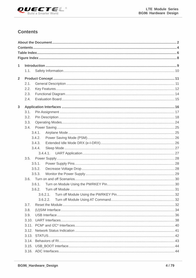
Contents
About the Document ................................................................................................................................... 2
Contents ....................................................................................................................................................... 4
Table Index ................................................................................................................................................... 6
Figure Index ................................................................................................................................................. 8
1 Introduction .......................................................................................................................................... 9
1.1. Safety Information ..................................................................................................................... 10
2 Product Concept ................................................................................................................................ 11
2.1. General Description .................................................................................................................. 11
2.2. Key Features ............................................................................................................................. 12
2.3. Functional Diagram ................................................................................................................... 14
2.4. Evaluation Board ....................................................................................................................... 15
3 Application Interfaces ....................................................................................................................... 16
3.1. Pin Assignment ......................................................................................................................... 17
3.2. Pin Description .......................................................................................................................... 18
3.3. Operating Modes ....................................................................................................................... 24
3.4. Power Saving ............................................................................................................................ 25
3.4.1. Airplane Mode ................................................................................................................ 25
3.4.2. Power Saving Mode (PSM) ............................................................................................ 26
3.4.3. Extended Idle Mode DRX (e-I-DRX) .............................................................................. 26
3.4.4. Sleep Mode .................................................................................................................... 27
3.4.4.1. UART Application ................................................................................................. 27
3.5. Power Supply ............................................................................................................................ 28
3.5.1. Power Supply Pins ......................................................................................................... 28
3.5.2. Decrease Voltage Drop .................................................................................................. 28
3.5.3. Monitor the Power Supply .............................................................................................. 29
3.6. Turn on and off Scenarios ......................................................................................................... 30
3.6.1. Turn on Module Using the PWRKEY Pin ....................................................................... 30
3.6.2. Turn off Module .............................................................................................................. 31
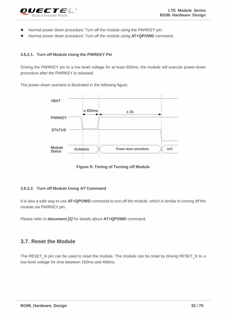
3.6.2.1. Turn off Module Using the PWRKEY Pin ............................................................. 32
3.6.2.2. Turn off Module Using AT Command ................................................................... 32
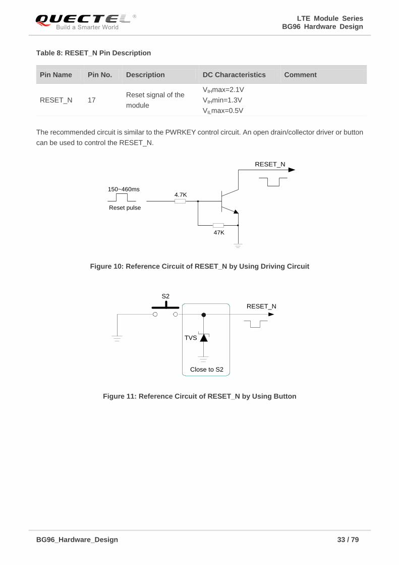
3.7. Reset the Module ...................................................................................................................... 32
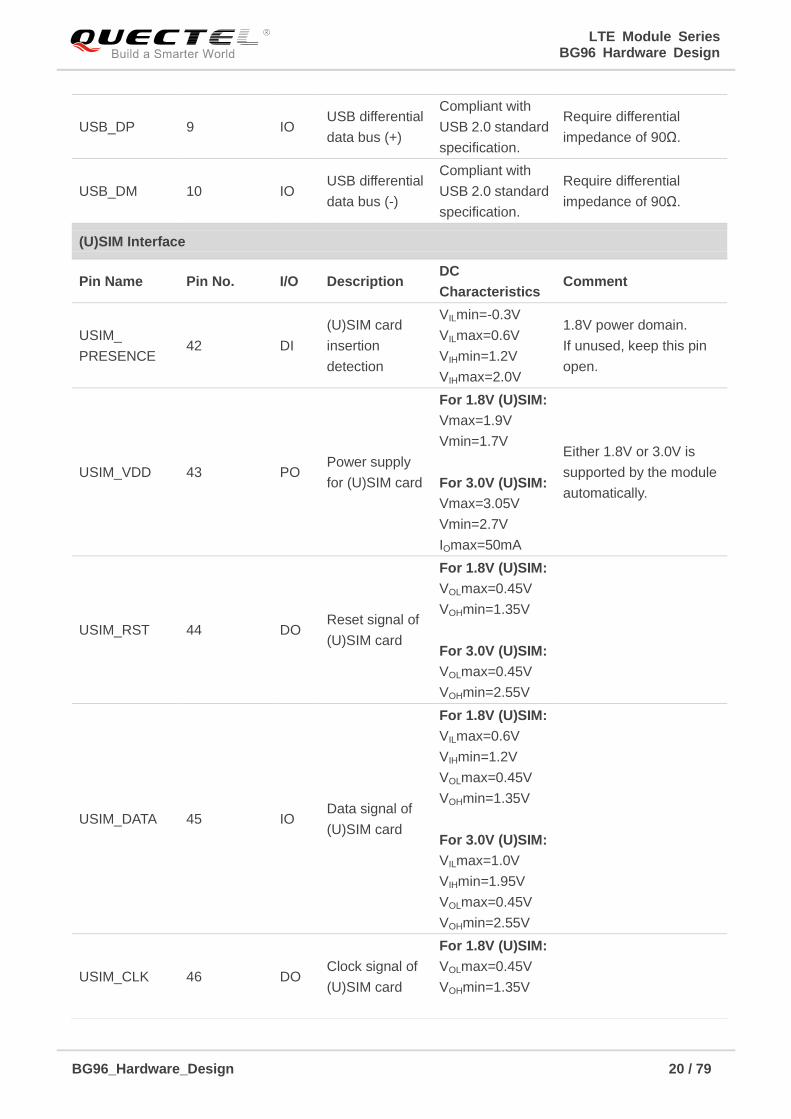
3.8. (U)SIM Interface ........................................................................................................................ 34
3.9. USB Interface ............................................................................................................................ 36
3.10. UART Interfaces ........................................................................................................................ 38
3.11. PCM* and I2C* Interfaces ......................................................................................................... 40
3.12. Network Status Indication ......................................................................................................... 41
3.13. STATUS ..................................................................................................................................... 42
3.14. Behaviors of RI .......................................................................................................................... 43
3.15. USB_BOOT Interface................................................................................................................ 44
3.16. ADC Interfaces .......................................................................................................................... 44
LTE Module Series BG96 Hardware Design
BG96_Hardware_Design 5 / 79
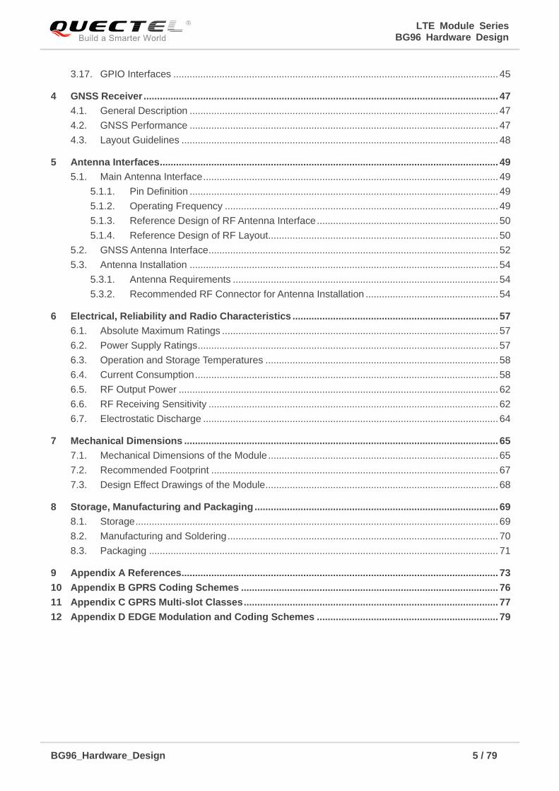
3.17. GPIO Interfaces ........................................................................................................................ 45
4 GNSS Receiver ................................................................................................................................... 47
4.1. General Description .................................................................................................................. 47
4.2. GNSS Performance .................................................................................................................. 47
4.3. Layout Guidelines ..................................................................................................................... 48
5 Antenna Interfaces ............................................................................................................................. 49
5.1. Main Antenna Interface ............................................................................................................. 49
5.1.1. Pin Definition .................................................................................................................. 49
5.1.2. Operating Frequency ..................................................................................................... 49
5.1.3. Reference Design of RF Antenna Interface ................................................................... 50
5.1.4. Reference Design of RF Layout..................................................................................... 50
5.2. GNSS Antenna Interface ........................................................................................................... 52
5.3. Antenna Installation .................................................................................................................. 54
5.3.1. Antenna Requirements .................................................................................................. 54
5.3.2. Recommended RF Connector for Antenna Installation ................................................. 54
6 Electrical, Reliability and Radio Characteristics ............................................................................ 57
6.1. Absolute Maximum Ratings ...................................................................................................... 57
6.2. Power Supply Ratings ............................................................................................................... 57
6.3. Operation and Storage Temperatures ...................................................................................... 58
6.4. Current Consumption ................................................................................................................ 58
6.5. RF Output Power ...................................................................................................................... 62
6.6. RF Receiving Sensitivity ........................................................................................................... 62
6.7. Electrostatic Discharge ............................................................................................................. 64
7 Mechanical Dimensions .................................................................................................................... 65
7.1. Mechanical Dimensions of the Module ..................................................................................... 65
7.2. Recommended Footprint .......................................................................................................... 67
7.3. Design Effect Drawings of the Module ...................................................................................... 68
8 Storage, Manufacturing and Packaging .......................................................................................... 69
8.1. Storage ...................................................................................................................................... 69
8.2. Manufacturing and Soldering .................................................................................................... 70
8.3. Packaging ................................................................................................................................. 71
9 Appendix A References ..................................................................................................................... 73
10 Appendix B GPRS Coding Schemes ............................................................................................... 76
11 Appendix C GPRS Multi-slot Classes .............................................................................................. 77
12 Appendix D EDGE Modulation and Coding Schemes ................................................................... 79
LTE Module Series BG96 Hardware Design
BG96_Hardware_Design 6 / 79
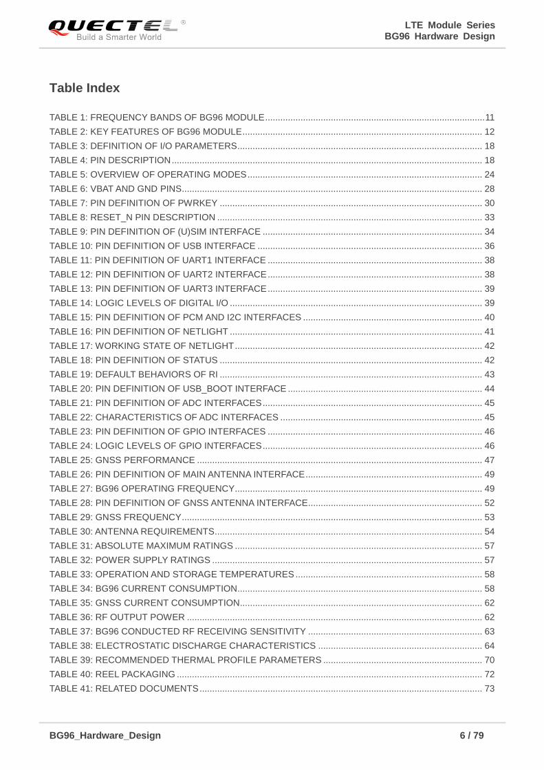
Table Index
TABLE 1: FREQUENCY BANDS OF BG96 MODULE ....................................................................................... 11
TABLE 2: KEY FEATURES OF BG96 MODULE ............................................................................................... 12
TABLE 3: DEFINITION OF I/O PARAMETERS ................................................................................................. 18
TABLE 4: PIN DESCRIPTION ........................................................................................................................... 18
TABLE 5: OVERVIEW OF OPERATING MODES ............................................................................................. 24
TABLE 6: VBAT AND GND PINS ....................................................................................................................... 28
TABLE 7: PIN DEFINITION OF PWRKEY ........................................................................................................ 30
TABLE 8: RESET_N PIN DESCRIPTION ......................................................................................................... 33
TABLE 9: PIN DEFINITION OF (U)SIM INTERFACE ....................................................................................... 34
TABLE 10: PIN DEFINITION OF USB INTERFACE ......................................................................................... 36
TABLE 11: PIN DEFINITION OF UART1 INTERFACE ..................................................................................... 38
TABLE 12: PIN DEFINITION OF UART2 INTERFACE ..................................................................................... 38
TABLE 13: PIN DEFINITION OF UART3 INTERFACE ..................................................................................... 39
TABLE 14: LOGIC LEVELS OF DIGITAL I/O .................................................................................................... 39
TABLE 15: PIN DEFINITION OF PCM AND I2C INTERFACES ....................................................................... 40
TABLE 16: PIN DEFINITION OF NETLIGHT .................................................................................................... 41
TABLE 17: WORKING STATE OF NETLIGHT .................................................................................................. 42
TABLE 18: PIN DEFINITION OF STATUS ........................................................................................................ 42
TABLE 19: DEFAULT BEHAVIORS OF RI ........................................................................................................ 43
TABLE 20: PIN DEFINITION OF USB_BOOT INTERFACE ............................................................................. 44
TABLE 21: PIN DEFINITION OF ADC INTERFACES ....................................................................................... 45
TABLE 22: CHARACTERISTICS OF ADC INTERFACES ................................................................................ 45
TABLE 23: PIN DEFINITION OF GPIO INTERFACES ..................................................................................... 46
TABLE 24: LOGIC LEVELS OF GPIO INTERFACES ....................................................................................... 46
TABLE 25: GNSS PERFORMANCE ................................................................................................................. 47
TABLE 26: PIN DEFINITION OF MAIN ANTENNA INTERFACE ...................................................................... 49
TABLE 27: BG96 OPERATING FREQUENCY .................................................................................................. 49
TABLE 28: PIN DEFINITION OF GNSS ANTENNA INTERFACE ..................................................................... 52
TABLE 29: GNSS FREQUENCY ....................................................................................................................... 53
TABLE 30: ANTENNA REQUIREMENTS .......................................................................................................... 54
TABLE 31: ABSOLUTE MAXIMUM RATINGS .................................................................................................. 57
TABLE 32: POWER SUPPLY RATINGS ........................................................................................................... 57
TABLE 33: OPERATION AND STORAGE TEMPERATURES .......................................................................... 58
TABLE 34: BG96 CURRENT CONSUMPTION ................................................................................................. 58
TABLE 35: GNSS CURRENT CONSUMPTION ................................................................................................ 62
TABLE 36: RF OUTPUT POWER ..................................................................................................................... 62
TABLE 37: BG96 CONDUCTED RF RECEIVING SENSITIVITY ..................................................................... 63
TABLE 38: ELECTROSTATIC DISCHARGE CHARACTERISTICS ................................................................. 64
TABLE 39: RECOMMENDED THERMAL PROFILE PARAMETERS ............................................................... 70
TABLE 40: REEL PACKAGING ......................................................................................................................... 72
TABLE 41: RELATED DOCUMENTS ................................................................................................................ 73
LTE Module Series BG96 Hardware Design
BG96_Hardware_Design 7 / 79
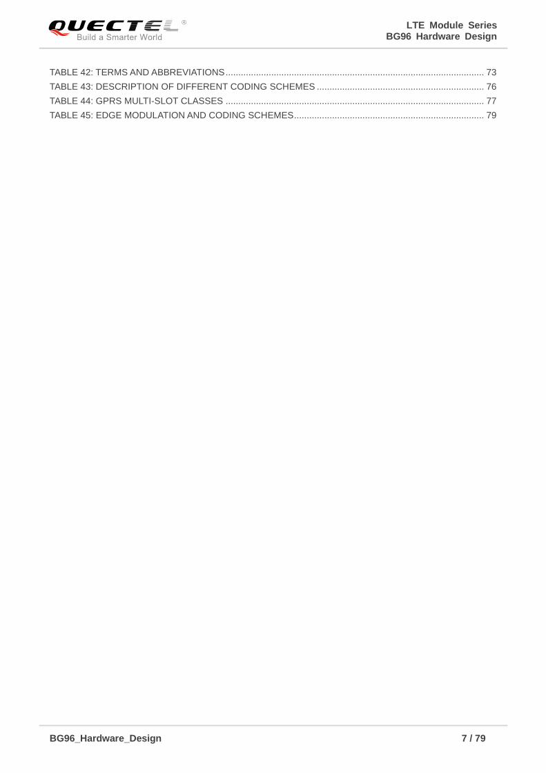
TABLE 42: TERMS AND ABBREVIATIONS ...................................................................................................... 73
TABLE 43: DESCRIPTION OF DIFFERENT CODING SCHEMES .................................................................. 76
TABLE 44: GPRS MULTI-SLOT CLASSES ...................................................................................................... 77
TABLE 45: EDGE MODULATION AND CODING SCHEMES ........................................................................... 79
LTE Module Series BG96 Hardware Design
BG96_Hardware_Design 8 / 79
Figure Index
FIGURE 1: FUNCTIONAL DIAGRAM ............................................................................................................... 14
FIGURE 2: PIN ASSIGNMENT (TOP VIEW)..................................................................................................... 17
FIGURE 3: SLEEP MODE APPLICATION VIA UART ....................................................................................... 27
FIGURE 4: POWER SUPPLY LIMITS DURING BURST TRANSMISSION ...................................................... 29
FIGURE 5: STAR STRUCTURE OF THE POWER SUPPLY............................................................................ 29
FIGURE 6: TURN ON THE MODULE USING DRIVING CIRCUIT ................................................................... 30
FIGURE 7: TURN ON THE MODULE USING KEYSTROKE ........................................................................... 31
FIGURE 8: TIMING OF TURNING ON MODULE ............................................................................................. 31
FIGURE 9: TIMING OF TURNING OFF MODULE ........................................................................................... 32
FIGURE 10: REFERENCE CIRCUIT OF RESET_N BY USING DRIVING CIRCUIT ...................................... 33
FIGURE 11: REFERENCE CIRCUIT OF RESET_N BY USING BUTTON ....................................................... 33
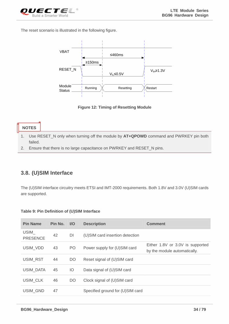
FIGURE 12: TIMING OF RESETTING MODULE ............................................................................................. 34
FIGURE 13: REFERENCE CIRCUIT OF (U)SIM INTERFACE WITH AN 8-PIN (U)SIM CARD CONNECTOR
................................................................................................................................................................... 35
FIGURE 14: REFERENCE CIRCUIT OF (U)SIM INTERFACE WITH A 6-PIN (U)SIM CARD CONNECTOR . 35
FIGURE 15: REFERENCE CIRCUIT OF USB INTERFACE ............................................................................ 37
FIGURE 16: REFERENCE CIRCUIT WITH TRANSLATOR CHIP ................................................................... 39
FIGURE 17: REFERENCE CIRCUIT WITH TRANSISTOR CIRCUIT .............................................................. 40
FIGURE 18: REFERENCE CIRCUIT OF PCM APPLICATION WITH AUDIO CODEC .................................... 41
FIGURE 19: REFERENCE CIRCUIT OF THE NETWORK STATUS INDICATOR ........................................... 42
FIGURE 20: REFERENCE CIRCUIT OF STATUS ........................................................................................... 43
FIGURE 21: REFERENCE CIRCUIT OF USB_BOOT INTERFACE ................................................................ 44
FIGURE 22: REFERENCE CIRCUIT OF RF ANTENNA INTERFACE ............................................................. 50
FIGURE 23: MICROSTRIP LINE DESIGN ON A 2-LAYER PCB ...................................................................... 51
FIGURE 24: COPLANAR WAVEGUIDE LINE DESIGN ON A 2-LAYER PCB .................................................. 51
FIGURE 25: COPLANAR WAVEGUIDE LINE DESIGN ON A 4-LAYER PCB (LAYER 3 AS REFERENCE
GROUND) .................................................................................................................................................. 51
FIGURE 26: COPLANAR WAVEGUIDE LINE DESIGN ON A 4-LAYER PCB (LAYER 4 AS REFERENCE
GROUND) .................................................................................................................................................. 52
FIGURE 27: REFERENCE CIRCUIT OF GNSS ANTENNA INTERFACE ........................................................ 53
FIGURE 28: DIMENSIONS OF THE U.FL-R-SMT CONNECTOR (UNIT: MM) ................................................ 55
FIGURE 29: MECHANICALS OF U.FL-LP CONNECTORS ............................................................................. 55
FIGURE 30: SPACE FACTOR OF MATED CONNECTOR (UNIT: MM) ........................................................... 56
FIGURE 31: MODULE TOP AND SIDE DIMENSIONS ..................................................................................... 65
FIGURE 32: MODULE BOTTOM DIMENSIONS (BOTTOM VIEW) ................................................................. 66
FIGURE 33: RECOMMENDED FOOTPRINT (TOP VIEW) .............................................................................. 67
FIGURE 34: TOP VIEW OF THE MODULE ...................................................................................................... 68
FIGURE 35: BOTTOM VIEW OF THE MODULE .............................................................................................. 68
FIGURE 36: RECOMMENDED REFLOW SOLDERING THERMAL PROFILE ................................................ 70
FIGURE 37: TAPE DIMENSIONS ..................................................................................................................... 71
FIGURE 38: REEL DIMENSIONS ..................................................................................................................... 72
LTE Module Series BG96 Hardware Design
BG96_Hardware_Design 9 / 79
1 Introduction
This document defines BG96 module and describes its air interface and hardware interfaces which are
connected with customers’ applications.
This document can help customers quickly understand the interface specifications, electrical and
mechanical details, as well as other related information of BG96. To facilitate its application in different
fields, reference design is also provided for customers’ reference. Associated with application notes and
user guides, customers can use the module to design and set up mobile applications easily.
LTE Module Series BG96 Hardware Design
BG96_Hardware_Design 10 / 79
1.1. Safety Information
The following safety precautions must be observed during all phases of the operation, such as usage,
service or repair of any cellular terminal or mobile incorporating BG96. Manufacturers of the cellular
terminal should send the following safety information to users and operating personnel, and incorporate
these guidelines into all manuals supplied with the product. If not so, Quectel assumes no liability for
customers’ failure to comply with these precautions.
Full attention must be given to driving at all times in order to reduce the risk of an
accident. Using a mobile while driving (even with a handsfree kit) causes
distraction and can lead to an accident. Please comply with laws and regulations
restricting the use of wireless devices while driving.
Switch off the cellular terminal or mobile before boarding an aircraft. The operation
of wireless appliances in an aircraft is forbidden to prevent interference with
communication systems. If the device offers an Airplane Mode, then it should be
enabled prior to boarding an aircraft. Please consult the airline staff for more
restrictions on the use of wireless devices on boarding the aircraft.
Wireless devices may cause interference on sensitive medical equipment, so
please be aware of the restrictions on the use of wireless devices when in
hospitals, clinics or other healthcare facilities.
Cellular terminals or mobiles operating over radio signals and cellular network
cannot be guaranteed to connect in all possible conditions (for example, with
unpaid bills or with an invalid (U)SIM card). When emergent help is needed in such
conditions, please remember using emergency call. In order to make or receive a
call, the cellular terminal or mobile must be switched on in a service area with
adequate cellular signal strength.
The cellular terminal or mobile contains a transmitter and receiver. When it is ON, it
receives and transmits radio frequency signals. RF interference can occur if it is
used close to TV set, radio, computer or other electric equipment.
In locations with potentially explosive atmospheres, obey all posted signs to turn
off wireless devices such as your phone or other cellular terminals. Areas with
potentially explosive atmospheres include fuelling areas, below decks on boats,
fuel or chemical transfer or storage facilities, areas where the air contains
chemicals or particles such as grain, dust or metal powders, etc.
LTE Module Series BG96 Hardware Design
BG96_Hardware_Design 11 / 79
2 Product Concept
2.1. General Description
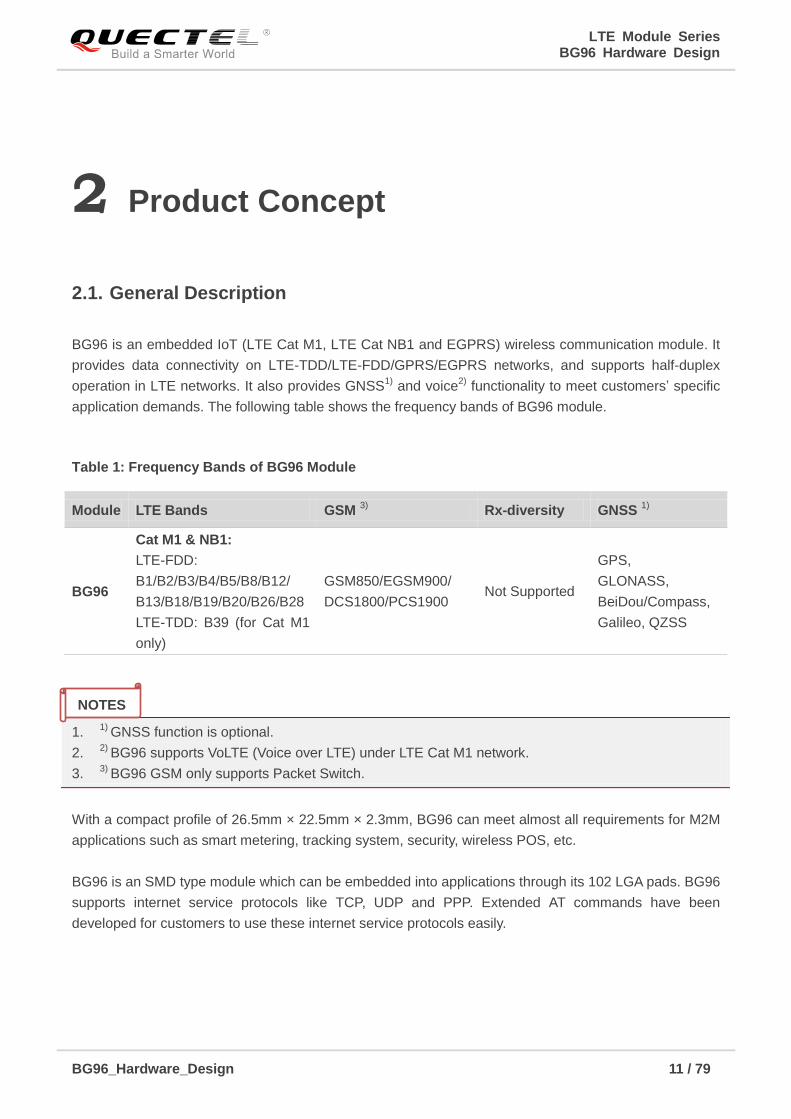
BG96 is an embedded IoT (LTE Cat M1, LTE Cat NB1 and EGPRS) wireless communication module. It
provides data connectivity on LTE-TDD/LTE-FDD/GPRS/EGPRS networks, and supports half-duplex
operation in LTE networks. It also provides GNSS1)
and voice2)
functionality to meet customers’ specific
application demands. The following table shows the frequency bands of BG96 module.
Table 1: Frequency Bands of BG96 Module
1. 1)
GNSS function is optional.
2. 2)
BG96 supports VoLTE (Voice over LTE) under LTE Cat M1 network.
3. 3)
BG96 GSM only supports Packet Switch.
With a compact profile of 26.5mm × 22.5mm × 2.3mm, BG96 can meet almost all requirements for M2M
applications such as smart metering, tracking system, security, wireless POS, etc.
BG96 is an SMD type module which can be embedded into applications through its 102 LGA pads. BG96
supports internet service protocols like TCP, UDP and PPP. Extended AT commands have been
developed for customers to use these internet service protocols easily.
Module LTE Bands GSM 3)
Rx-diversity GNSS 1)
BG96
Cat M1 & NB1:
LTE-FDD:
B1/B2/B3/B4/B5/B8/B12/
B13/B18/B19/B20/B26/B28
LTE-TDD: B39 (for Cat M1
only)
GSM850/EGSM900/
DCS1800/PCS1900 Not Supported
GPS,
GLONASS,
BeiDou/Compass,
Galileo, QZSS
NOTES
LTE Module Series BG96 Hardware Design
BG96_Hardware_Design 12 / 79
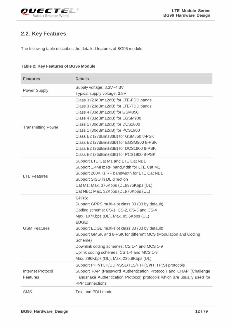
2.2. Key Features
The following table describes the detailed features of BG96 module.
Table 2: Key Features of BG96 Module
Features Details
Power Supply Supply voltage: 3.3V~4.3V
Typical supply voltage: 3.8V
Transmitting Power
Class 3 (23dBm±2dB) for LTE-FDD bands
Class 3 (23dBm±2dB) for LTE-TDD bands
Class 4 (33dBm±2dB) for GSM850
Class 4 (33dBm±2dB) for EGSM900
Class 1 (30dBm±2dB) for DCS1800
Class 1 (30dBm±2dB) for PCS1900
Class E2 (27dBm±3dB) for GSM850 8-PSK
Class E2 (27dBm±3dB) for EGSM900 8-PSK
Class E2 (26dBm±3dB) for DCS1800 8-PSK
Class E2 (26dBm±3dB) for PCS1900 8-PSK
LTE Features
Support LTE Cat M1 and LTE Cat NB1
Support 1.4MHz RF bandwidth for LTE Cat M1
Support 200KHz RF bandwidth for LTE Cat NB1
Support SISO in DL direction
Cat M1: Max. 375Kbps (DL)/375Kbps (UL)
Cat NB1: Max. 32Kbps (DL)/70Kbps (UL)
GSM Features
GPRS:
Support GPRS multi-slot class 33 (33 by default)
Coding scheme: CS-1, CS-2, CS-3 and CS-4
Max. 107Kbps (DL), Max. 85.6Kbps (UL)
EDGE:
Support EDGE multi-slot class 33 (33 by default)
Support GMSK and 8-PSK for different MCS (Modulation and Coding
Scheme)
Downlink coding schemes: CS 1-4 and MCS 1-9
Uplink coding schemes: CS 1-4 and MCS 1-9
Max. 296Kbps (DL), Max. 236.8Kbps (UL)
Internet Protocol
Features
Support PPP/TCP/UDP/SSL/TLS/FTP(S)/HTTP(S) protocols
Support PAP (Password Authentication Protocol) and CHAP (Challenge
Handshake Authentication Protocol) protocols which are usually used for
PPP connections
SMS Text and PDU mode
LTE Module Series BG96 Hardware Design
BG96_Hardware_Design 13 / 79
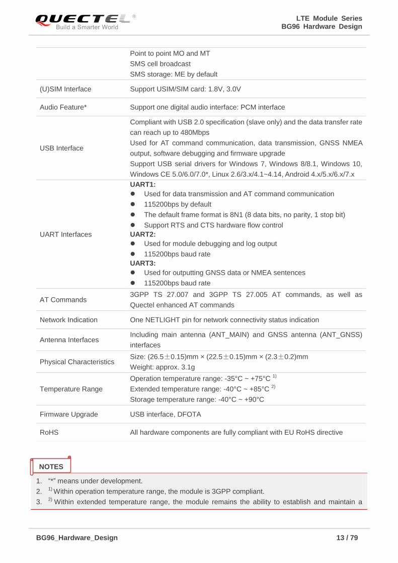
1. “*” means under development.
2. 1)
Within operation temperature range, the module is 3GPP compliant.
3. 2)
Within extended temperature range, the module remains the ability to establish and maintain a
Point to point MO and MT
SMS cell broadcast
SMS storage: ME by default
(U)SIM Interface Support USIM/SIM card: 1.8V, 3.0V
Audio Feature* Support one digital audio interface: PCM interface
USB Interface
Compliant with USB 2.0 specification (slave only) and the data transfer rate
can reach up to 480Mbps
Used for AT command communication, data transmission, GNSS NMEA
output, software debugging and firmware upgrade
Support USB serial drivers for Windows 7, Windows 8/8.1, Windows 10,
Windows CE 5.0/6.0/7.0*, Linux 2.6/3.x/4.1~4.14, Android 4.x/5.x/6.x/7.x
UART Interfaces
UART1:
Used for data transmission and AT command communication
115200bps by default
The default frame format is 8N1 (8 data bits, no parity, 1 stop bit)
Support RTS and CTS hardware flow control
UART2:
Used for module debugging and log output
115200bps baud rate
UART3:
Used for outputting GNSS data or NMEA sentences
115200bps baud rate
AT Commands 3GPP TS 27.007 and 3GPP TS 27.005 AT commands, as well as
Quectel enhanced AT commands
Network Indication One NETLIGHT pin for network connectivity status indication
Antenna Interfaces Including main antenna (ANT_MAIN) and GNSS antenna (ANT_GNSS)
interfaces
Physical Characteristics Size: (26.5±0.15)mm × (22.5±0.15)mm × (2.3±0.2)mm
Weight: approx. 3.1g
Temperature Range
Operation temperature range: -35°C ~ +75°C 1)
Extended temperature range: -40°C ~ +85°C 2)
Storage temperature range: -40°C ~ +90°C
Firmware Upgrade USB interface, DFOTA
RoHS All hardware components are fully compliant with EU RoHS directive
NOTES
LTE Module Series BG96 Hardware Design
BG96_Hardware_Design 14 / 79
voice, SMS, data transmission, emergency call, etc. There is no unrecoverable malfunction. There
are also no effects on radio spectrum and no harm to radio network. Only one or more parameters like
Pout might reduce in their value and exceed the specified tolerances. When the temperature returns to
the normal operating temperature levels, the module will meet 3GPP specifications again.
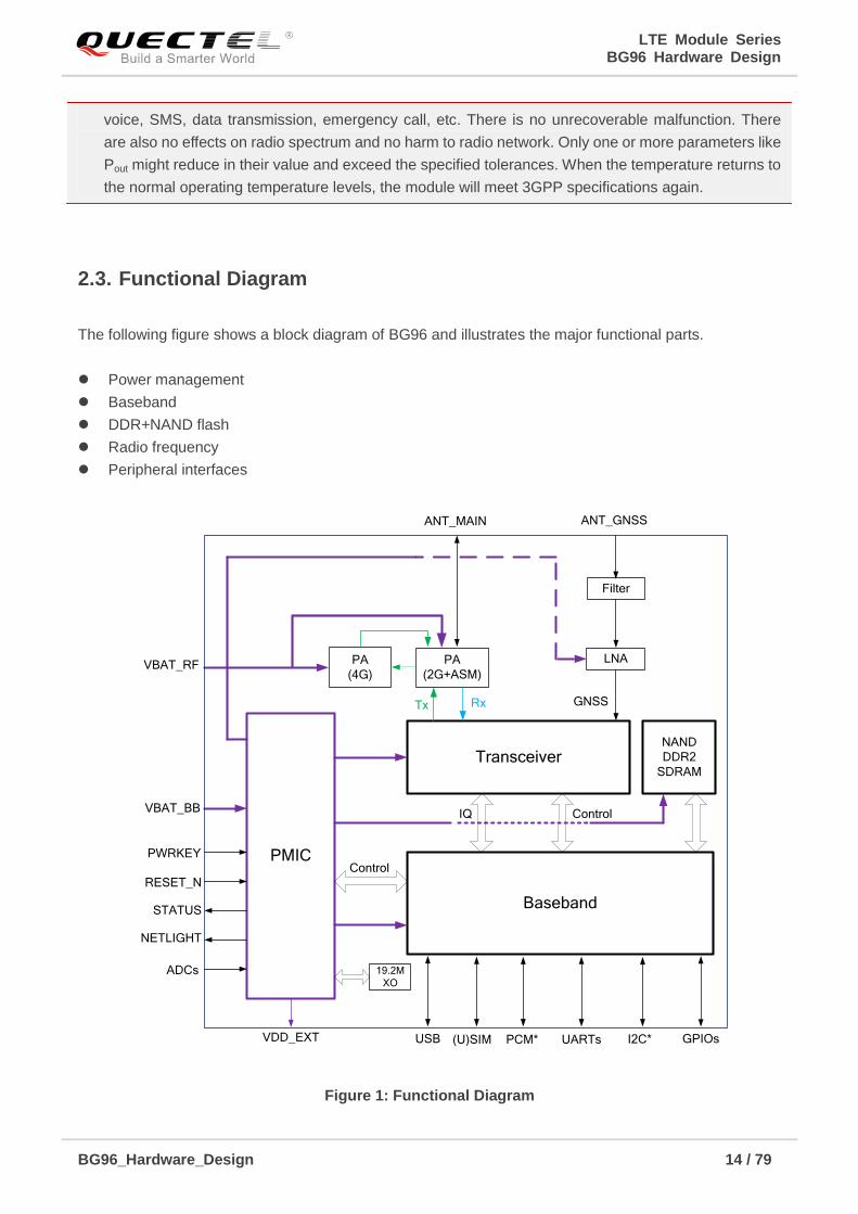
2.3. Functional Diagram
The following figure shows a block diagram of BG96 and illustrates the major functional parts.
Power management
Baseband
DDR+NAND flash
Radio frequency
Peripheral interfaces
Baseband
PMIC
TransceiverNAND
DDR2
SDRAM
PA
(2G+ASM)
Filter
ANT_MAIN ANT_GNSS
VBAT_BB
VBAT_RF
PWRKEY
VDD_EXT USB (U)SIM PCM* I2C*
RESET_N
19.2M
XO
STATUS
GPIOs
Control
IQ Control
LNA
Tx Rx GNSS
UARTs
NETLIGHT
PA
(4G)
ADCs
Figure 1: Functional Diagram
LTE Module Series BG96 Hardware Design
BG96_Hardware_Design 15 / 79
“*” means under development.
2.4. Evaluation Board
In order to help customers develop applications conveniently with BG96, Quectel supplies the evaluation
board (EVB), USB to RS-232 converter cable, USB data cable, earphone, antenna and other peripherals
to control or test the module. For more details, please refer to document [1].
NOTE
LTE Module Series BG96 Hardware Design
BG96_Hardware_Design 16 / 79
3 Application Interfaces
BG96 is equipped with 102 LGA pads that can be connected to customers’ cellular application platforms.
The following sub-chapters will provide detailed description of interfaces listed below:
Power supply
(U)SIM interface
USB interface
UART interfaces
PCM* and I2C* interfaces
Status indication
USB_BOOT interface
ADC interfaces
GPIO interfaces
“*” means under development.
NOTE
LTE Module Series BG96 Hardware Design
BG96_Hardware_Design 17 / 79
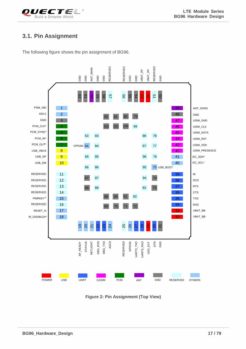
3.1. Pin Assignment
The following figure shows the pin assignment of BG96.
PSM_IND
PCM_SYNC*
PCM_CLK*
PCM_IN*
PCM_OUT*
RESERVED
RESERVED
PWRKEY1)
RESERVED
RESET_N
W_DISABLE#*
1
2
3
4
5
6
7
11
12
13
14
15
16
17
50
51
52
53
54
55
58
59
60
61
62
USB_DM
AP
_R
EA
DY
ST
AT
US
NE
TL
IGH
T
DB
G_
RX
D
DB
G_T
XD
AD
C0
RE
SE
RV
ED
GP
IO2
6
UA
RT
3_
TX
D
UA
RT
3_
RX
D
VD
D_
EX
T
DT
R
GN
D
USIM_CLK
USIM_DATA
USIM_RST
USIM_VDD
RI
DCD
CTS
TXD
RXD
VBAT_BB
VBAT_BB
USIM_GND
GND
RE
SE
RV
ED
31
30
29
28
27
26
23
22
21
20
19
10
9USB_DP
USB_VBUS
ADC1
GND
RESERVED
RESERVED
RTS
I2C_SCL*
I2C_SDA*
8
49
48
47
46
45
44
43
40
41
42
39
38
37
36
35
34
33
32
24
57
56
GN
D
GN
D
AN
T_M
AIN
GN
D
GN
D
VB
AT
_R
F
VB
AT
_R
F
GN
D
GN
D
ANT_GNSS
RE
SE
RV
ED
GN
D
USIM_PRESENCE
63
64
65
66
67
68
83
84
85
86
87
88
98
97
96
95
94
93
78
77
76
75
74
73
91 9289 90
71 7269 70
80 7982 81
100 99102 101
POWER USB UART (U)SIM OTHERSGND RESERVEDPCM ANT
25
RE
SE
RV
ED
USB_BOOT
18
GPIO64
Figure 2: Pin Assignment (Top View)
LTE Module Series BG96 Hardware Design
BG96_Hardware_Design 18 / 79
1. Keep all RESERVED pins and unused pins unconnected.
2. GND pads should be connected to ground in the design.
3. 1)
PWRKEY output voltage is 0.8V because of the diode drop in the Qualcomm chipset.
4. “*” means under development.
3.2. Pin Description
The following tables show the pin definition and description of BG96.
Table 3: Definition of I/O Parameters
Table 4: Pin Description
Type Description
IO Bidirectional
DI Digital input
DO Digital output
PI Power input
PO Power output
AI Analog input
AO Analog output
OD Open drain
Power Supply
Pin Name Pin No. I/O Description DC
Characteristics Comment
VBAT_BB 32, 33 PI
Power supply
for the
module’s
baseband part
Vmax=4.3V
Vmin=3.3V
Vnorm=3.8V
NOTES
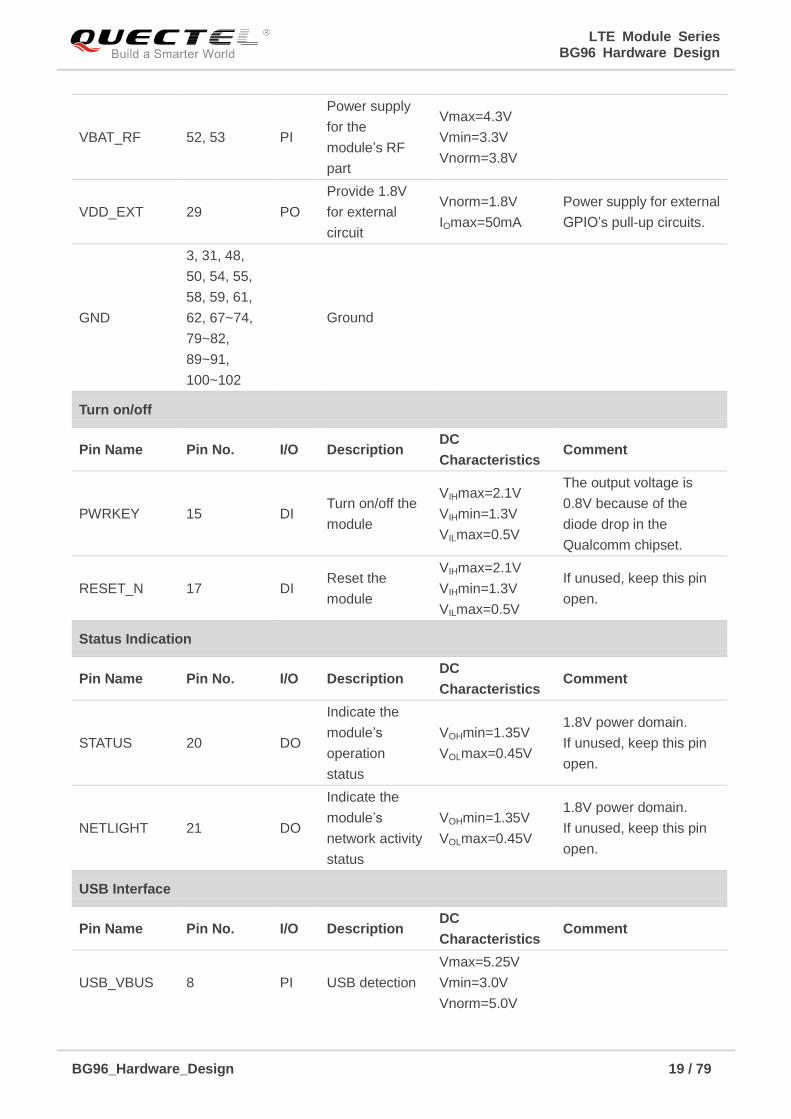
LTE Module Series BG96 Hardware Design
BG96_Hardware_Design 19 / 79
VBAT_RF 52, 53 PI
Power supply
for the
module’s RF
part
Vmax=4.3V
Vmin=3.3V
Vnorm=3.8V
VDD_EXT 29 PO
Provide 1.8V
for external
circuit
Vnorm=1.8V
IOmax=50mA
Power supply for external
GPIO’s pull-up circuits.
GND
3, 31, 48,
50, 54, 55,
58, 59, 61,
62, 67~74,
79~82,
89~91,
100~102
Ground
Turn on/off
Pin Name Pin No. I/O Description DC
Characteristics Comment
PWRKEY 15 DI Turn on/off the
module
VIHmax=2.1V
VIHmin=1.3V
VILmax=0.5V
The output voltage is
0.8V because of the
diode drop in the
Qualcomm chipset.
RESET_N 17 DI Reset the
module
VIHmax=2.1V
VIHmin=1.3V
VILmax=0.5V
If unused, keep this pin
open.
Status Indication
Pin Name Pin No. I/O Description DC
Characteristics Comment
STATUS 20 DO
Indicate the
module’s
operation
status
VOHmin=1.35V
VOLmax=0.45V
1.8V power domain.
If unused, keep this pin
open.
NETLIGHT 21 DO
Indicate the
module’s
network activity
status
VOHmin=1.35V
VOLmax=0.45V
1.8V power domain.
If unused, keep this pin
open.
USB Interface
Pin Name Pin No. I/O Description DC
Characteristics Comment
USB_VBUS 8 PI USB detection
Vmax=5.25V
Vmin=3.0V
Vnorm=5.0V
LTE Module Series BG96 Hardware Design
BG96_Hardware_Design 20 / 79
USB_DP 9 IO USB differential
data bus (+)
Compliant with
USB 2.0 standard
specification.
Require differential
impedance of 90Ω.
USB_DM 10 IO USB differential
data bus (-)
Compliant with
USB 2.0 standard
specification.
Require differential
impedance of 90Ω.
(U)SIM Interface
Pin Name Pin No. I/O Description DC
Characteristics Comment
USIM_
PRESENCE 42 DI
(U)SIM card
insertion
detection
VILmin=-0.3V
VILmax=0.6V
VIHmin=1.2V
VIHmax=2.0V
1.8V power domain.
If unused, keep this pin
open.
USIM_VDD 43 PO Power supply
for (U)SIM card
For 1.8V (U)SIM:
Vmax=1.9V
Vmin=1.7V
For 3.0V (U)SIM:
Vmax=3.05V
Vmin=2.7V
IOmax=50mA
Either 1.8V or 3.0V is
supported by the module
automatically.
USIM_RST 44 DO Reset signal of
(U)SIM card
For 1.8V (U)SIM:
VOLmax=0.45V
VOHmin=1.35V
For 3.0V (U)SIM:
VOLmax=0.45V
VOHmin=2.55V
USIM_DATA 45 IO Data signal of
(U)SIM card
For 1.8V (U)SIM:
VILmax=0.6V
VIHmin=1.2V
VOLmax=0.45V
VOHmin=1.35V
For 3.0V (U)SIM:
VILmax=1.0V
VIHmin=1.95V
VOLmax=0.45V
VOHmin=2.55V
USIM_CLK 46 DO Clock signal of
(U)SIM card
For 1.8V (U)SIM:
VOLmax=0.45V
VOHmin=1.35V
LTE Module Series BG96 Hardware Design
BG96_Hardware_Design 21 / 79
For 3.0V (U)SIM:
VOLmax=0.45V
VOHmin=2.55V
USIM_GND 47
Specified
ground for
(U)SIM card
UART1 Interface
Pin Name Pin No. I/O Description DC
Characteristics Comment
DTR 30 DI
Data terminal
ready(sleep
mode control)
VILmin=-0.3V
VILmax=0.6V
VIHmin=1.2V
VIHmax=2.0V
1.8V power domain.
If unused, keep this pin
open.
RXD 34 DI Receive data
VILmin=-0.3V
VILmax=0.6V
VIHmin=1.2V
VIHmax=2.0V
1.8V power domain.
If unused, keep this pin
open.
TXD 35 DO Transmit data VOLmax=0.45V
VOHmin=1.35V
1.8V power domain.
If unused, keep this pin
open.
CTS 36 DO Clear to send VOLmax=0.45V
VOHmin=1.35V
1.8V power domain.
If unused, keep this pin
open.
RTS 37 DI Request to
send
VILmin=-0.3V
VILmax=0.6V
VIHmin=1.2V
VIHmax=2.0V
1.8V power domain.
If unused, keep this pin
open.
DCD 38 DO Data carrier
detection
VOLmax=0.45V
VOHmin=1.35V
1.8V power domain.
If unused, keep this pin
open.
RI 39 DO Ring indicator VOLmax=0.45V
VOHmin=1.35V
1.8V power domain.
If unused, keep this pin
open.
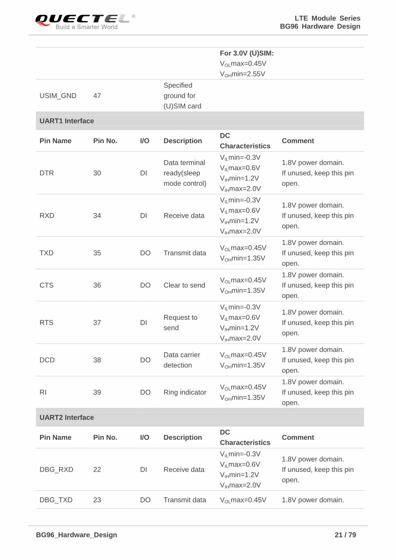
UART2 Interface
Pin Name Pin No. I/O Description DC
Characteristics Comment
DBG_RXD 22 DI Receive data
VILmin=-0.3V
VILmax=0.6V
VIHmin=1.2V
VIHmax=2.0V
1.8V power domain.
If unused, keep this pin
open.
DBG_TXD 23 DO Transmit data VOLmax=0.45V 1.8V power domain.
LTE Module Series BG96 Hardware Design
BG96_Hardware_Design 22 / 79
VOHmin=1.35V If unused, keep this pin
open.
UART3 Interface
Pin Name Pin No. I/O Description DC
Characteristics Comment
UART3_TXD 27 DO Transmit data VOLmax=0.45V
VOHmin=1.35V
1.8V power domain.
If unused, keep this pin
open.
UART3_RXD 28 DI Receive data
VILmin=-0.3V
VILmax=0.6V
VIHmin=1.2V
VIHmax=2.0V
1.8V power domain.
If unused, keep this pin
open.
PCM* Interface
Pin Name Pin No. I/O Description DC
Characteristics Comment
PCM_CLK* 4 DO PCM clock
output
VOLmax=0.45V
VOHmin=1.35V
1.8V power domain.
If unused, keep this pin
open.
PCM_SYNC* 5 DO
PCM frame
synchronization
output
VOLmax=0.45V
VOHmin=1.35V
1.8V power domain. If unused, keep this pin open.
PCM_IN* 6 DI PCM data input
VILmin=-0.3V
VILmax=0.6V
VIHmin=1.2V
VIHmax=2.0V
1.8V power domain.
If unused, keep this pin
open.
PCM_OUT* 7 DO PCM data
output
VOLmax=0.45V
VOHmin=1.35V
1.8V power domain.
If unused, keep this pin
open.
I2C* Interface
Pin Name Pin No. I/O Description DC
Characteristics Comment
I2C_SCL* 40 OD
I2C serial clock.
Used for
external codec.
External pull-up resistor
is required.
1.8V only. If unused,
keep this pin open.
I2C_SDA* 41 OD
I2C serial data.
Used for
external codec.
External pull-up resistor
is required.
1.8V only. If unused,
keep this pin open.
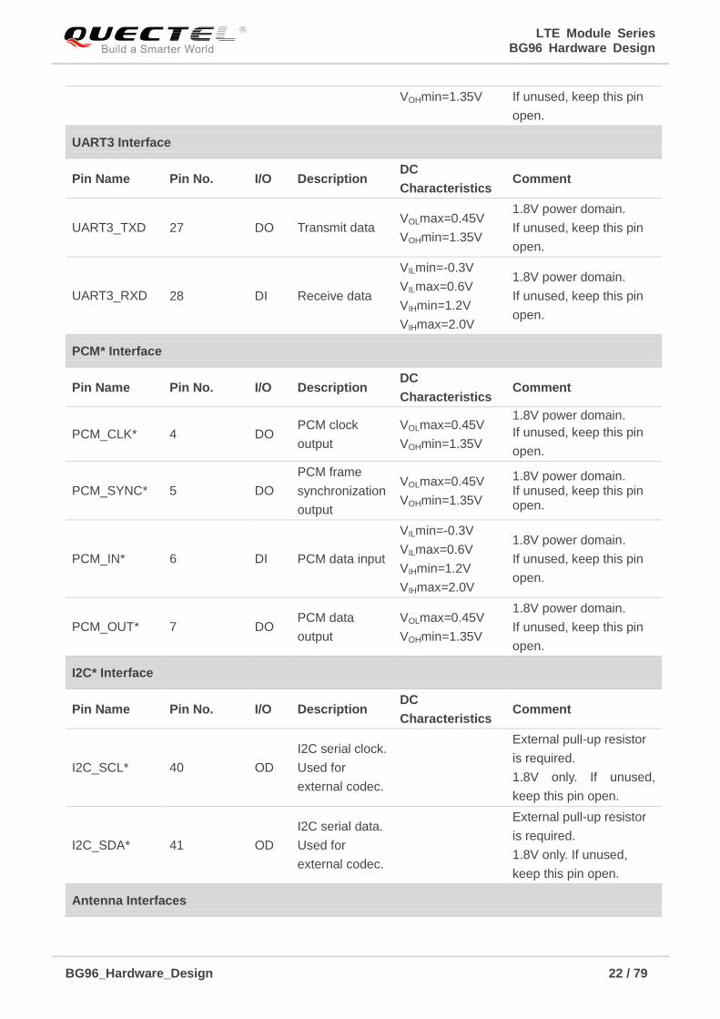
Antenna Interfaces
LTE Module Series BG96 Hardware Design
BG96_Hardware_Design 23 / 79
Pin Name Pin No. I/O Description DC
Characteristics Comment
ANT_MAIN 60 IO Main antenna
interface 50Ω impedance
ANT_GNSS 49 AI GNSS antenna
interface 50Ω impedance
If unused, keep this pin
open.
Other Pins
Pin Name Pin No. I/O Description DC
Characteristics Comment
PSM_IND 1 DO Power saving
mode indicator
VOLmax=0.45V
VOHmin=1.35V
1.8V power domain.
If unused, keep this pin
open.
W_DISABLE#* 18 DI Airplane mode
control
VILmin=-0.3V
VILmax=0.6V
VIHmin=1.2V
VIHmax=2.0V
1.8V power domain.
Pull-up by default.
In low voltage level, the
module can enter into
airplane mode.
If unused, keep this pin
open.
AP_READY 19 DI
Application
processor
sleep state
detection
VILmin=-0.3V
VILmax=0.6V
VIHmin=1.2V
VIHmax=2.0V
1.8V power domain.
If unused, keep this pin
open.
USB_BOOT 75 DI
Force the
module to enter
into emergency
download
mode
VILmin=-0.3V
VILmax=0.6V
VIHmin=1.2V
VIHmax=2.0V
1.8V power domain.
If unused, keep this pin
open.
GPIO26 26 IO
General-
purpose input/
output interface
VOLmax=0.45V
VOHmin=1.35V
VILmin=-0.3V
VILmax=0.6V
VIHmin=1.2V
VIHmax=2.0V
1.8V power domain.
If unused, keep this pin
open.
GPIO64 64 IO
General-
purpose input/
output interface
VOLmax=0.45V
VOHmin=1.35V
VILmin=-0.3V
VILmax=0.6V
VIHmin=1.2V
VIHmax=2.0V
1.8V power domain.
If unused, keep this pin
open.
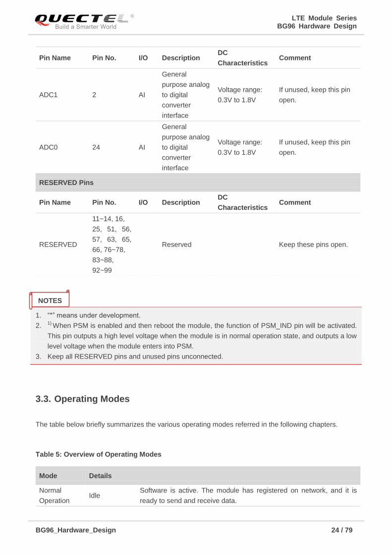
ADC Interfaces
LTE Module Series BG96 Hardware Design
BG96_Hardware_Design 24 / 79
1. “*” means under development.
2. 1)
When PSM is enabled and then reboot the module, the function of PSM_IND pin will be activated.
This pin outputs a high level voltage when the module is in normal operation state, and outputs a low
level voltage when the module enters into PSM.
3. Keep all RESERVED pins and unused pins unconnected.
3.3. Operating Modes
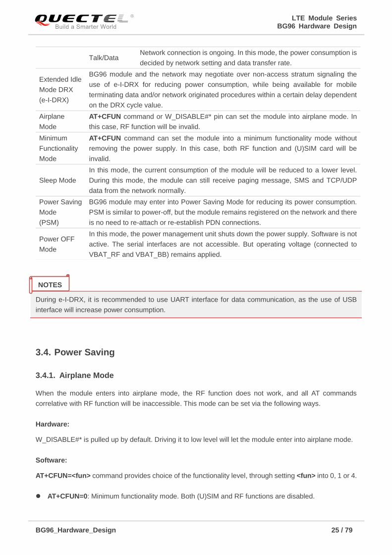
The table below briefly summarizes the various operating modes referred in the following chapters.
Table 5: Overview of Operating Modes
Pin Name Pin No. I/O Description DC
Characteristics Comment
ADC1 2 AI
General
purpose analog
to digital
converter
interface
Voltage range:
0.3V to 1.8V
If unused, keep this pin
open.
ADC0 24 AI
General
purpose analog
to digital
converter
interface
Voltage range:
0.3V to 1.8V
If unused, keep this pin
open.
RESERVED Pins
Pin Name Pin No. I/O Description DC
Characteristics Comment
RESERVED
11~14, 16,
25, 51, 56,
57, 63, 65,
66, 76~78,
83~88,
92~99
Reserved Keep these pins open.
Mode Details
Normal
Operation Idle
Software is active. The module has registered on network, and it is
ready to send and receive data.
NOTES
LTE Module Series BG96 Hardware Design
BG96_Hardware_Design 25 / 79
During e-I-DRX, it is recommended to use UART interface for data communication, as the use of USB
interface will increase power consumption.
3.4. Power Saving
3.4.1. Airplane Mode
When the module enters into airplane mode, the RF function does not work, and all AT commands
correlative with RF function will be inaccessible. This mode can be set via the following ways.
Hardware:
W_DISABLE#* is pulled up by default. Driving it to low level will let the module enter into airplane mode.
Software:
AT+CFUN=<fun> command provides choice of the functionality level, through setting <fun> into 0, 1 or 4.
AT+CFUN=0: Minimum functionality mode. Both (U)SIM and RF functions are disabled.
Talk/Data Network connection is ongoing. In this mode, the power consumption is
decided by network setting and data transfer rate.
Extended Idle
Mode DRX
(e-I-DRX)
BG96 module and the network may negotiate over non-access stratum signaling the
use of e-I-DRX for reducing power consumption, while being available for mobile
terminating data and/or network originated procedures within a certain delay dependent
on the DRX cycle value.
Airplane
Mode
AT+CFUN command or W_DISABLE#* pin can set the module into airplane mode. In
this case, RF function will be invalid.
Minimum
Functionality
Mode
AT+CFUN command can set the module into a minimum functionality mode without
removing the power supply. In this case, both RF function and (U)SIM card will be
invalid.
Sleep Mode
In this mode, the current consumption of the module will be reduced to a lower level.
During this mode, the module can still receive paging message, SMS and TCP/UDP
data from the network normally.
Power Saving
Mode
(PSM)
BG96 module may enter into Power Saving Mode for reducing its power consumption.
PSM is similar to power-off, but the module remains registered on the network and there
is no need to re-attach or re-establish PDN connections.
Power OFF
Mode
In this mode, the power management unit shuts down the power supply. Software is not
active. The serial interfaces are not accessible. But operating voltage (connected to
VBAT_RF and VBAT_BB) remains applied.
NOTES
LTE Module Series BG96 Hardware Design
BG96_Hardware_Design 26 / 79
AT+CFUN=1: Full functionality mode (by default).
AT+CFUN=4: Airplane mode. RF function is disabled.
1. Airplane mode control via W_DISABLE# is disabled in firmware by default. It can be enabled by
AT+QCFG=“airplanecontrol” command. The command is still under development.
2. The execution of AT+CFUN command will not affect GNSS function.
3. “*” means under development.
3.4.2. Power Saving Mode (PSM)
BG96 module can enter into PSM for reducing its power consumption. The mode is similar to power-off,
but the module remains registered on the network and there is no need to re-attach or re-establish PDN
connections. So BG96 in PSM cannot immediately respond users’ requests.
When the module wants to use the PSM it shall request an Active Time value during every Attach and
TAU procedures. If the network supports PSM and accepts that the module uses PSM, the network
confirms usage of PSM by allocating an Active Time value to the module. If the module wants to change
the Active Time value, e.g. when the conditions are changed in the module, the module consequently
requests the value it wants in the TAU procedure.
If PSM is supported by the network, then it can be enabled via AT+CPSMS command.
Either of the following methods will wake up the module from PSM:
Drive PWRKEY pin to low level will wake up the module.
When the T3412_Ext timer expires, the module will be automatically woken up.
Please refer to document [2] for details about AT+CPSMS command.
3.4.3. Extended Idle Mode DRX (e-I-DRX)
The module (UE) and the network may negotiate over non-access stratum signalling the use of e-I-DRX
for reducing its power consumption, while being available for mobile terminating data and/or network
originated procedures within a certain delay dependent on the DRX cycle value.
Applications that want to use e-I-DRX need to consider specific handling of mobile terminating services or
data transfers, and in particular they need to consider the delay tolerance of mobile terminated data.
NOTES
NOTE
LTE Module Series BG96 Hardware Design
BG96_Hardware_Design 27 / 79
In order to negotiate the use of e-I-DRX, the UE requests e-I-DRX parameters during attach procedure
and RAU/TAU procedure. The EPC may reject or accept the UE request for enabling e-I-DRX. In case the
EPC accepts e-I-DRX, the EPC based on operator policies and, if available, the e-I-DRX cycle length
value in the subscription data from the HSS, may also provide different values of the e-I-DRX parameters
than what was requested by the UE. If the EPC accepts the use of e-I-DRX, the UE applies e-I-DRX
based on the received e-I-DRX parameters. If the UE does not receive e-I-DRX parameters in the
relevant accept message because the EPC rejected its request or because the request was received by
EPC not supporting e-I-DRX, the UE shall apply its regular discontinuous reception.
If e-I-DRX is supported by the network, then it can be enabled by AT+CEDRXS=1 command.
Please refer to document [2] for details about AT+CEDRXS command.
3.4.4. Sleep Mode
BG96 is able to reduce its current consumption to a lower value during the sleep mode. The following
sub-chapters describe the power saving procedure of BG96 module.
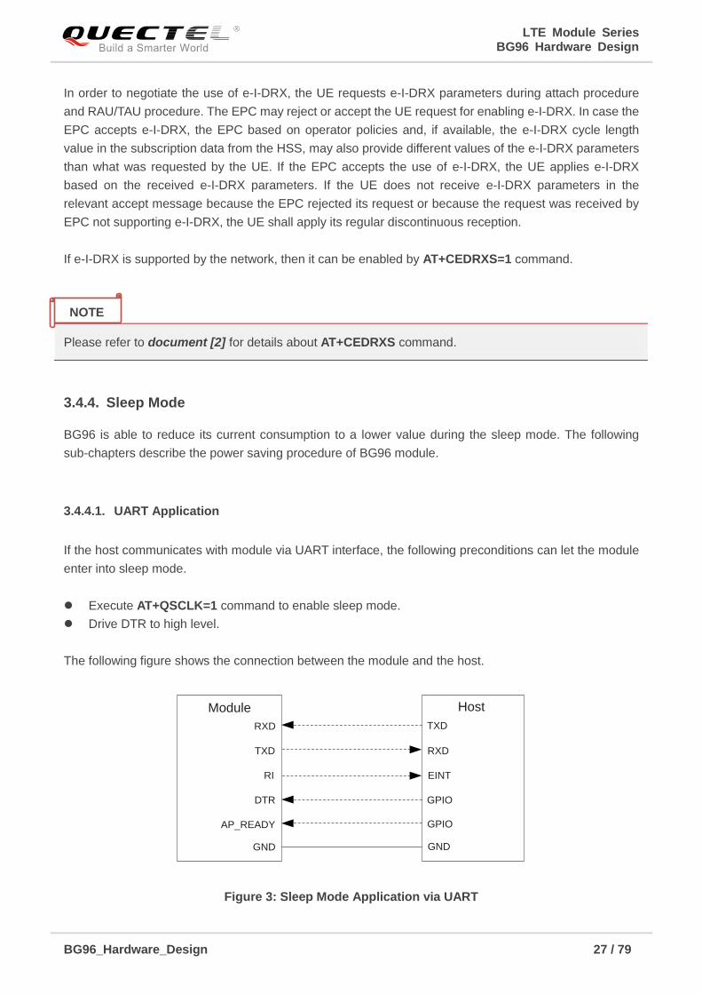
3.4.4.1. UART Application
If the host communicates with module via UART interface, the following preconditions can let the module
enter into sleep mode.
Execute AT+QSCLK=1 command to enable sleep mode.
Drive DTR to high level.
The following figure shows the connection between the module and the host.
RXD
TXD
RI
DTR
AP_READY
TXD
RXD
EINT
GPIO
GPIO
Module Host
GND GND
Figure 3: Sleep Mode Application via UART
NOTE
LTE Module Series BG96 Hardware Design
BG96_Hardware_Design 28 / 79
Driving the host DTR to low level will wake up the module.
When BG96 has URC to report, RI signal will wake up the host. Please refer to Chapter 3.14 for
details about RI behavior.
AP_READY will detect the sleep state of the host (can be configured to high level or low level
detection). Please refer to AT+QCFG=“apready” command in document [2] for details.
3.5. Power Supply
3.5.1. Power Supply Pins
BG96 provides the following four VBAT pins for connection with an external power supply. There are two
separate voltage domains for VBAT.
Two VBAT_RF pins for module’s RF part.
Two VBAT_BB pins for module’s baseband part.
The following table shows the details of VBAT pins and ground pins.
Table 6: VBAT and GND Pins
3.5.2. Decrease Voltage Drop
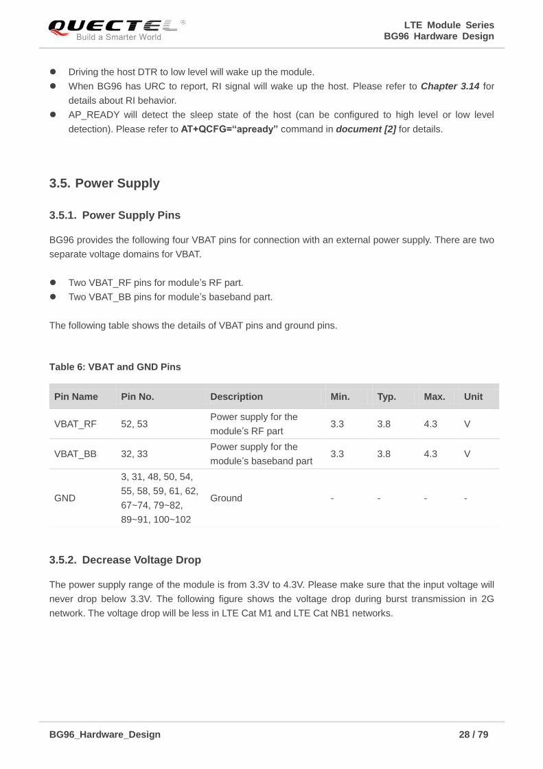
The power supply range of the module is from 3.3V to 4.3V. Please make sure that the input voltage will
never drop below 3.3V. The following figure shows the voltage drop during burst transmission in 2G
network. The voltage drop will be less in LTE Cat M1 and LTE Cat NB1 networks.
Pin Name Pin No. Description Min. Typ. Max. Unit
VBAT_RF 52, 53 Power supply for the
module’s RF part 3.3 3.8 4.3 V
VBAT_BB 32, 33 Power supply for the
module’s baseband part 3.3 3.8 4.3 V
GND
3, 31, 48, 50, 54,
55, 58, 59, 61, 62,
67~74, 79~82,
89~91, 100~102
Ground - - - -
LTE Module Series BG96 Hardware Design
BG96_Hardware_Design 29 / 79
VBAT
Burst Transmission
Min.3.3V
Ripple
Drop
Burst Transmission
Figure 4: Power Supply Limits during Burst Transmission
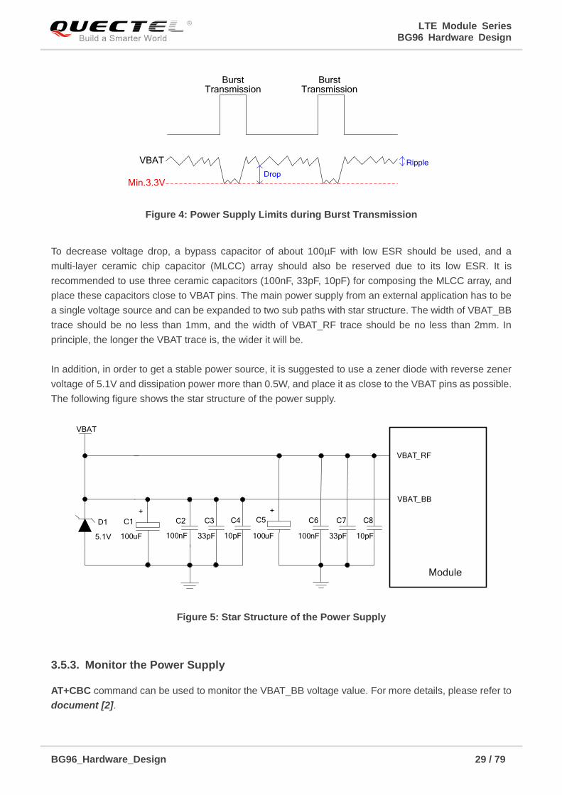
To decrease voltage drop, a bypass capacitor of about 100µF with low ESR should be used, and a
multi-layer ceramic chip capacitor (MLCC) array should also be reserved due to its low ESR. It is
recommended to use three ceramic capacitors (100nF, 33pF, 10pF) for composing the MLCC array, and
place these capacitors close to VBAT pins. The main power supply from an external application has to be
a single voltage source and can be expanded to two sub paths with star structure. The width of VBAT_BB
trace should be no less than 1mm, and the width of VBAT_RF trace should be no less than 2mm. In
principle, the longer the VBAT trace is, the wider it will be.
In addition, in order to get a stable power source, it is suggested to use a zener diode with reverse zener
voltage of 5.1V and dissipation power more than 0.5W, and place it as close to the VBAT pins as possible.
The following figure shows the star structure of the power supply.
Module
VBAT_RF
VBAT_BB
VBAT
C1
100uF
C6
100nF
C7
33pF
C8
10pF
++
C2
100nF
C5
100uF
C3
33pF
C4
10pF
D1
5.1V
Figure 5: Star Structure of the Power Supply
3.5.3. Monitor the Power Supply
AT+CBC command can be used to monitor the VBAT_BB voltage value. For more details, please refer to
document [2].
LTE Module Series BG96 Hardware Design
BG96_Hardware_Design 30 / 79
3.6. Turn on and off Scenarios
3.6.1. Turn on Module Using the PWRKEY Pin
The following table shows the pin definition of PWRKEY.
Table 7: Pin Definition of PWRKEY
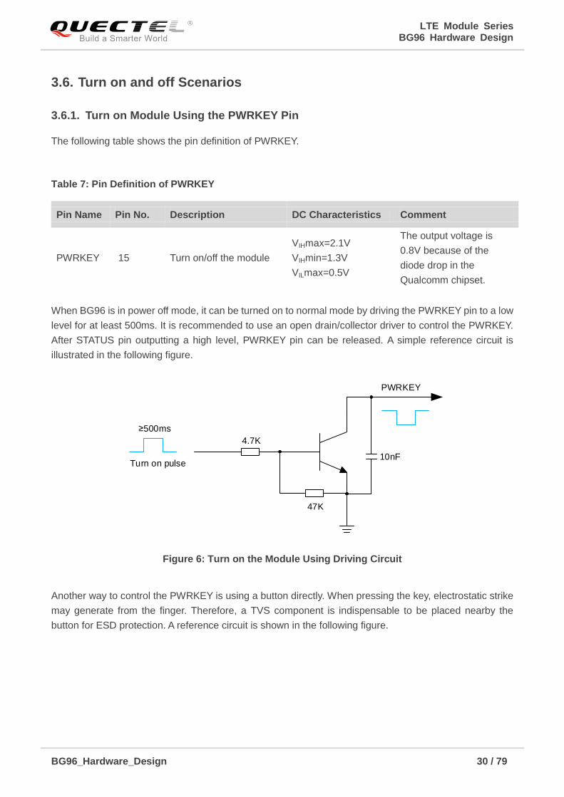
When BG96 is in power off mode, it can be turned on to normal mode by driving the PWRKEY pin to a low
level for at least 500ms. It is recommended to use an open drain/collector driver to control the PWRKEY.
After STATUS pin outputting a high level, PWRKEY pin can be released. A simple reference circuit is
illustrated in the following figure.
Turn on pulse
PWRKEY
4.7K
47K
≥500ms
10nF
Figure 6: Turn on the Module Using Driving Circuit
Another way to control the PWRKEY is using a button directly. When pressing the key, electrostatic strike
may generate from the finger. Therefore, a TVS component is indispensable to be placed nearby the
button for ESD protection. A reference circuit is shown in the following figure.
Pin Name Pin No. Description DC Characteristics Comment
PWRKEY 15 Turn on/off the module
VIHmax=2.1V
VIHmin=1.3V
VILmax=0.5V
The output voltage is
0.8V because of the
diode drop in the
Qualcomm chipset.
LTE Module Series BG96 Hardware Design
BG96_Hardware_Design 31 / 79
PWRKEY
S1
Close to S1
TVS
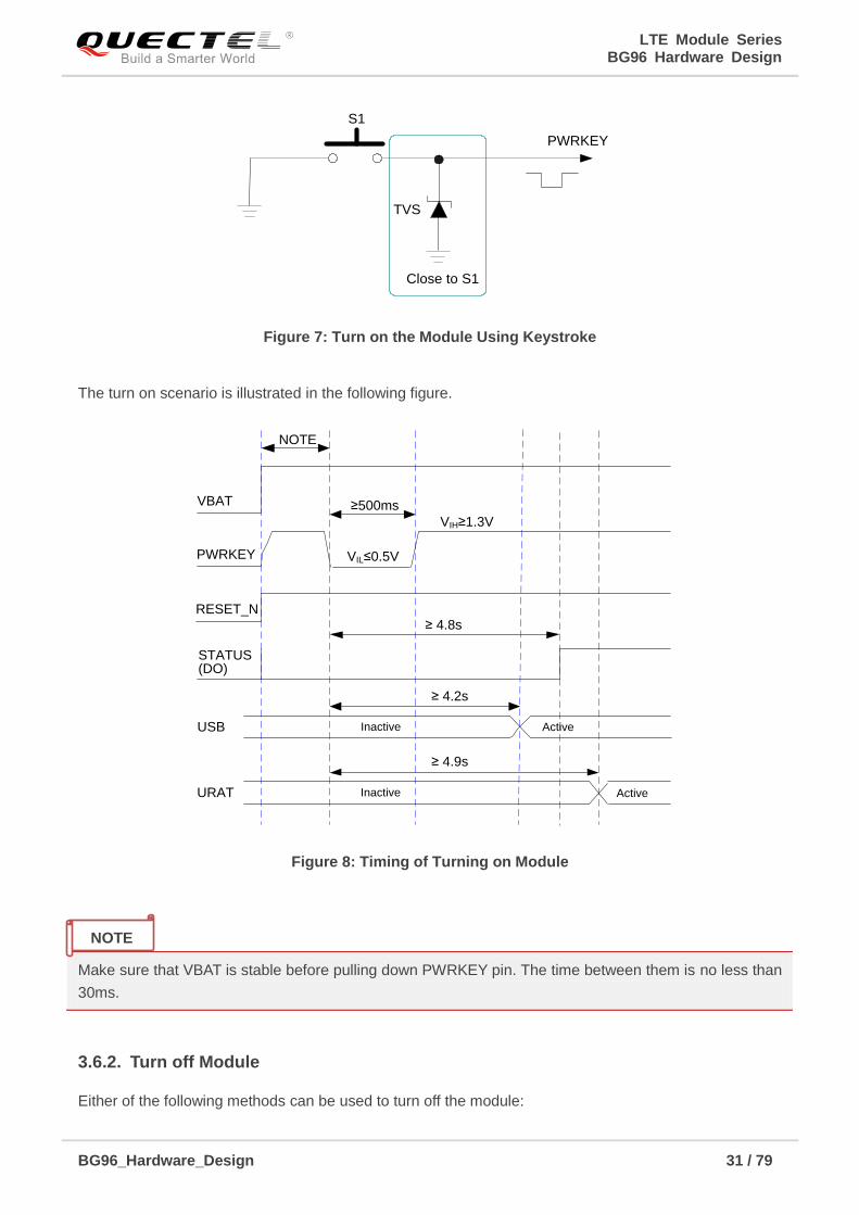
Figure 7: Turn on the Module Using Keystroke
The turn on scenario is illustrated in the following figure.
VIL≤0.5V
VIH≥1.3V
VBAT
PWRKEY
≥500ms
RESET_N
STATUS(DO)
Inactive ActiveUSB
NOTE
Inactive ActiveURAT
≥ 4.8s
≥ 4.2s
≥ 4.9s
Figure 8: Timing of Turning on Module
Make sure that VBAT is stable before pulling down PWRKEY pin. The time between them is no less than
30ms.
3.6.2. Turn off Module
Either of the following methods can be used to turn off the module:
NOTE
LTE Module Series BG96 Hardware Design
BG96_Hardware_Design 32 / 79
Normal power down procedure: Turn off the module using the PWRKEY pin.
Normal power down procedure: Turn off the module using AT+QPOWD command.
3.6.2.1. Turn off Module Using the PWRKEY Pin
Driving the PWRKEY pin to a low level voltage for at least 650ms, the module will execute power-down
procedure after the PWRKEY is released.
The power-down scenario is illustrated in the following figure.
VBAT
PWRKEY
≥ 2s≥ 650ms
RUNNING Power-down procedure OFFModuleStatus
STATUS
Figure 9: Timing of Turning off Module
3.6.2.2. Turn off Module Using AT Command
It is also a safe way to use AT+QPOWD command to turn off the module, which is similar to turning off the
module via PWRKEY pin.
Please refer to document [2] for details about AT+QPOWD command.
3.7. Reset the Module
The RESET_N pin can be used to reset the module. The module can be reset by driving RESET_N to a
low level voltage for time between 150ms and 460ms.
LTE Module Series BG96 Hardware Design
BG96_Hardware_Design 33 / 79
Table 8: RESET_N Pin Description
The recommended circuit is similar to the PWRKEY control circuit. An open drain/collector driver or button
can be used to control the RESET_N.
Reset pulse
RESET_N
4.7K
47K
150~460ms
Figure 10: Reference Circuit of RESET_N by Using Driving Circuit
RESET_N
S2
Close to S2
TVS
Figure 11: Reference Circuit of RESET_N by Using Button
Pin Name Pin No. Description DC Characteristics Comment
RESET_N 17 Reset signal of the
module
VIHmax=2.1V
VIHmin=1.3V
VILmax=0.5V
LTE Module Series BG96 Hardware Design
BG96_Hardware_Design 34 / 79
The reset scenario is illustrated in the following figure.
VBAT
≥150ms
ResettingModule
StatusRunning
RESET_N
Restart
≤460ms
VIL≤0.5VVIH≥1.3V
Figure 12: Timing of Resetting Module
1. Use RESET_N only when turning off the module by AT+QPOWD command and PWRKEY pin both
failed.
2. Ensure that there is no large capacitance on PWRKEY and RESET_N pins.
3.8. (U)SIM Interface
The (U)SIM interface circuitry meets ETSI and IMT-2000 requirements. Both 1.8V and 3.0V (U)SIM cards
are supported.
Table 9: Pin Definition of (U)SIM Interface
Pin Name Pin No. I/O Description Comment
USIM_
PRESENCE 42 DI (U)SIM card insertion detection
USIM_VDD 43 PO Power supply for (U)SIM card Either 1.8V or 3.0V is supported
by the module automatically.
USIM_RST 44 DO Reset signal of (U)SIM card
USIM_DATA 45 IO Data signal of (U)SIM card
USIM_CLK 46 DO Clock signal of (U)SIM card
USIM_GND 47 Specified ground for (U)SIM card
NOTES
LTE Module Series BG96 Hardware Design
BG96_Hardware_Design 35 / 79
BG96 supports (U)SIM card hot-plug via the USIM_PRESENCE pin. The function supports low level and
high level detections, and is disabled by default. Please refer to document [2] about AT+QSIMDET
command for details.
The following figure shows a reference design of (U)SIM interface with an 8-pin (U)SIM card connector.
Module
USIM_VDD
USIM_GND
USIM_RST
USIM_CLK
USIM_DATA
USIM_PRESENCE
0R
0R
0R
VDD_EXT
51K
100nF (U)SIM Card Connector
GND
GND33pF 33pF 33pF
VCC
RST
CLK IO
VPP
GND
GND
USIM_VDD
15K
Figure 13: Reference Circuit of (U)SIM Interface with an 8-Pin (U)SIM Card Connector
If (U)SIM card detection function is not needed, please keep USIM_PRESENCE unconnected. A
reference circuit for (U)SIM interface with a 6-pin (U)SIM card connector is illustrated in the following
figure.
Module
USIM_VDD
USIM_GND
USIM_RST
USIM_CLK
USIM_DATA 0R
0R
0R
100nF(U)SIM Card Connector
GND
33pF 33pF 33pF
VCC
RST
CLK IO
VPP
GND
GND
15K
USIM_VDD
Figure 14: Reference Circuit of (U)SIM Interface with a 6-Pin (U)SIM Card Connector
LTE Module Series BG96 Hardware Design
BG96_Hardware_Design 36 / 79
In order to enhance the reliability and availability of the (U)SIM card in applications, please follow the
criteria below in (U)SIM circuit design:
Keep placement of (U)SIM card connector as close to the module as possible. Keep the trace length
as less than 200mm as possible.
Keep (U)SIM card signals away from RF and VBAT traces.
Assure the ground between the module and the (U)SIM card connector short and wide. Keep the
trace width of ground and USIM_VDD no less than 0.5mm to maintain the same electric potential.
Make sure the bypass capacitor between USIM_VDD and USIM_GND less than 1uF, and place it as
close to (U)SIM card connector as possible. If the system ground plane is complete, USIM_GND can
be connected to the system ground directly.
To avoid cross-talk between USIM_DATA and USIM_CLK, keep them away from each other and
shield them with surrounded ground. USIM_RST should also be ground shielded.
In order to offer good ESD protection, it is recommended to add a TVS diode array with parasitic
capacitance not exceeding 15pF. In order to facilitate debugging, it is recommended to reserve series
resistors for the (U)SIM signals of the module. The 33pF capacitors are used for filtering interference
of GSM 900MHz. Please note that the (U)SIM peripheral circuit should be close to the (U)SIM card
connector.
The pull-up resistor on USIM_DATA line can improve anti-jamming capability when long layout trace
and sensitive occasion are applied, and should be placed close to the (U)SIM card connector.
3.9. USB Interface
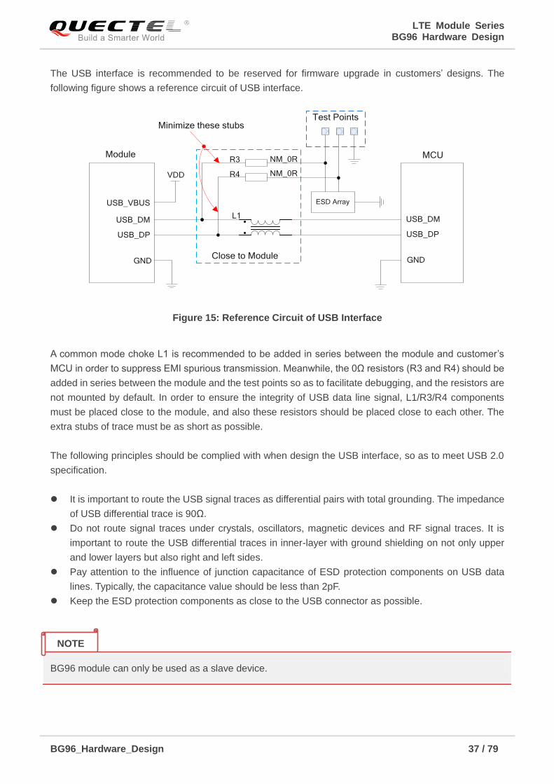
BG96 contains one integrated Universal Serial Bus (USB) interface which complies with the USB 2.0
specification and supports high-speed (480Mbps) and full-speed (12Mbps) modes. The USB interface is
used for AT command communication, data transmission, software debugging and firmware upgrade. The
following table shows the pin definition of USB interface.
Table 10: Pin Definition of USB Interface
For more details about USB 2.0 specification, please visit http://www.usb.org/home.
Pin Name Pin No. I/O Description Comment
USB_VBUS 8 PI USB connection detection Typically 5.0V
USB_DP 9 IO USB differential data bus (+) Require differential
impedance of 90Ω
USB_DM 10 IO USB differential data bus (-) Require differential
impedance of 90Ω
GND 3 Ground
LTE Module Series BG96 Hardware Design
BG96_Hardware_Design 37 / 79
The USB interface is recommended to be reserved for firmware upgrade in customers’ designs. The
following figure shows a reference circuit of USB interface.
USB_DP
USB_DM
GND
USB_DP
USB_DM
GND
L1
Close to Module
R3
R4
Test Points
ESD Array
NM_0R
NM_0R
Minimize these stubs
Module MCU
USB_VBUS
VDD
Figure 15: Reference Circuit of USB Interface
A common mode choke L1 is recommended to be added in series between the module and customer’s
MCU in order to suppress EMI spurious transmission. Meanwhile, the 0Ω resistors (R3 and R4) should be
added in series between the module and the test points so as to facilitate debugging, and the resistors are
not mounted by default. In order to ensure the integrity of USB data line signal, L1/R3/R4 components
must be placed close to the module, and also these resistors should be placed close to each other. The
extra stubs of trace must be as short as possible.
The following principles should be complied with when design the USB interface, so as to meet USB 2.0
specification.
It is important to route the USB signal traces as differential pairs with total grounding. The impedance
of USB differential trace is 90Ω.
Do not route signal traces under crystals, oscillators, magnetic devices and RF signal traces. It is
important to route the USB differential traces in inner-layer with ground shielding on not only upper
and lower layers but also right and left sides.
Pay attention to the influence of junction capacitance of ESD protection components on USB data
lines. Typically, the capacitance value should be less than 2pF.
Keep the ESD protection components as close to the USB connector as possible.
BG96 module can only be used as a slave device.
NOTE
LTE Module Series BG96 Hardware Design
BG96_Hardware_Design 38 / 79
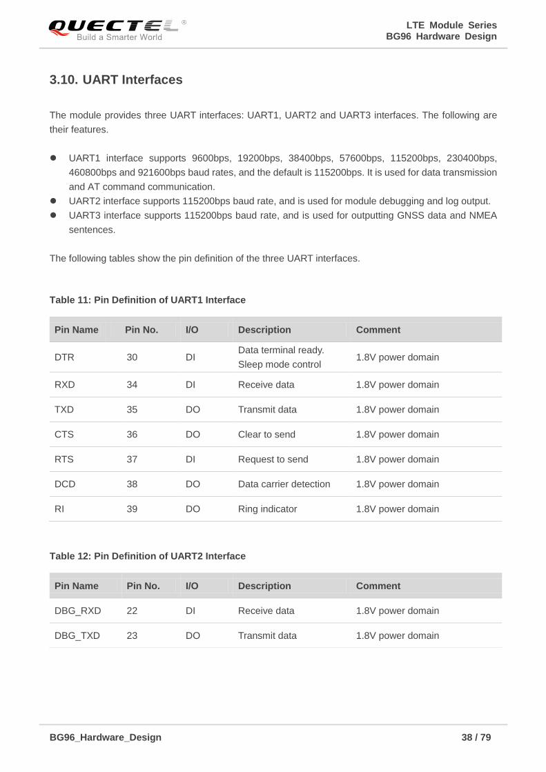
3.10. UART Interfaces
The module provides three UART interfaces: UART1, UART2 and UART3 interfaces. The following are
their features.
UART1 interface supports 9600bps, 19200bps, 38400bps, 57600bps, 115200bps, 230400bps,
460800bps and 921600bps baud rates, and the default is 115200bps. It is used for data transmission
and AT command communication.
UART2 interface supports 115200bps baud rate, and is used for module debugging and log output.
UART3 interface supports 115200bps baud rate, and is used for outputting GNSS data and NMEA
sentences.
The following tables show the pin definition of the three UART interfaces.
Table 11: Pin Definition of UART1 Interface
Table 12: Pin Definition of UART2 Interface
Pin Name Pin No. I/O Description Comment
DTR 30 DI Data terminal ready.
Sleep mode control 1.8V power domain
RXD 34 DI Receive data 1.8V power domain
TXD 35 DO Transmit data 1.8V power domain
CTS 36 DO Clear to send 1.8V power domain
RTS 37 DI Request to send 1.8V power domain
DCD 38 DO Data carrier detection 1.8V power domain
RI 39 DO Ring indicator 1.8V power domain
Pin Name Pin No. I/O Description Comment
DBG_RXD 22 DI Receive data 1.8V power domain
DBG_TXD 23 DO Transmit data 1.8V power domain
LTE Module Series BG96 Hardware Design
BG96_Hardware_Design 39 / 79
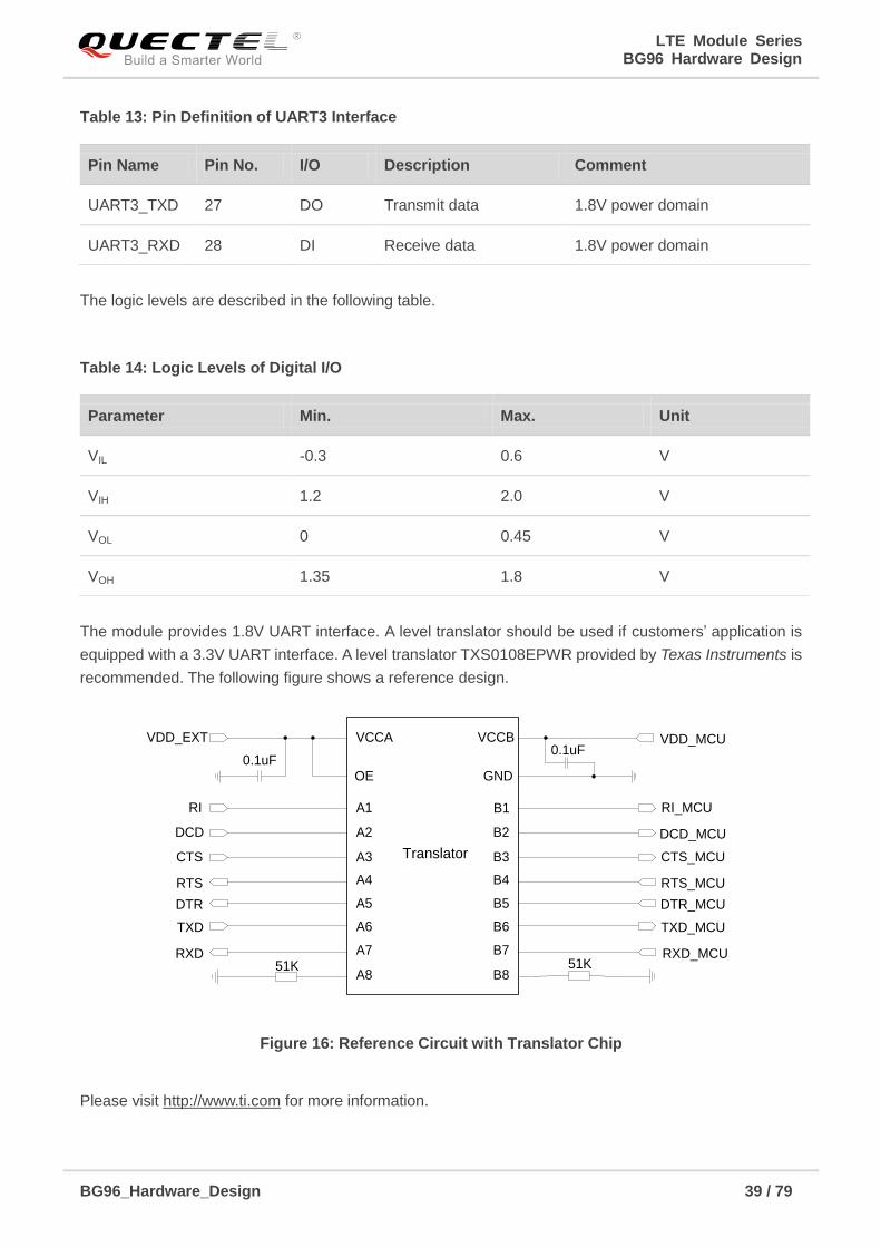
Table 13: Pin Definition of UART3 Interface
The logic levels are described in the following table.
Table 14: Logic Levels of Digital I/O
The module provides 1.8V UART interface. A level translator should be used if customers’ application is
equipped with a 3.3V UART interface. A level translator TXS0108EPWR provided by Texas Instruments is
recommended. The following figure shows a reference design.
VCCA VCCB
OE
A1
A2
A3
A4
A5
A6
A7
A8
GND
B1
B2
B3
B4
B5
B6
B7
B8
VDD_EXT
RI
DCD
RTS
RXD
DTR
CTS
TXD
51K 51K
0.1uF0.1uF
RI_MCU
DCD_MCU
RTS_MCU
RXD_MCU
DTR_MCU
CTS_MCU
TXD_MCU
VDD_MCU
Translator
Figure 16: Reference Circuit with Translator Chip
Please visit http://www.ti.com for more information.
Pin Name Pin No. I/O Description Comment
UART3_TXD 27 DO Transmit data 1.8V power domain
UART3_RXD 28 DI Receive data 1.8V power domain
Parameter Min. Max. Unit
VIL -0.3 0.6 V
VIH 1.2 2.0 V
VOL 0 0.45 V
VOH 1.35 1.8 V
LTE Module Series BG96 Hardware Design
BG96_Hardware_Design 40 / 79
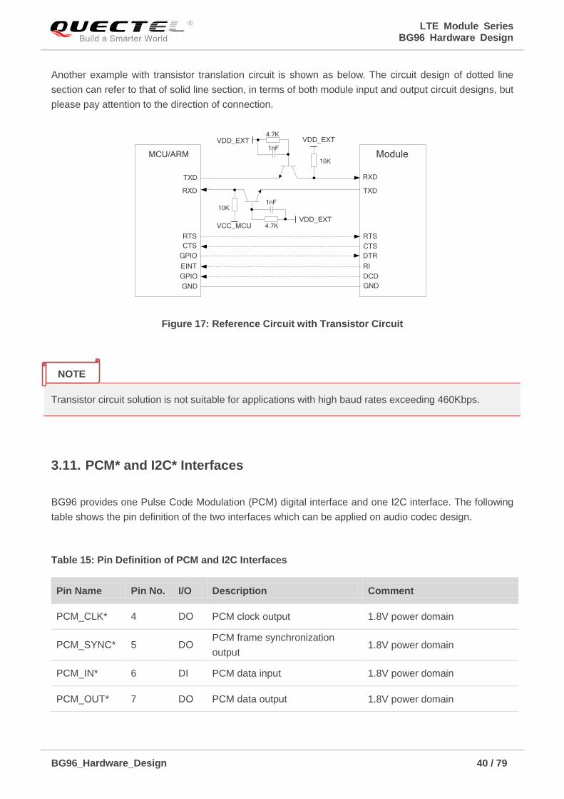
Another example with transistor translation circuit is shown as below. The circuit design of dotted line
section can refer to that of solid line section, in terms of both module input and output circuit designs, but
please pay attention to the direction of connection.
MCU/ARM
TXD
RXD
VDD_EXT
10K
VCC_MCU 4.7K
10K
VDD_EXT
TXD
RXD
RTS
CTS
DTR
RI
RTS
CTS
GND
GPIO DCD
Module
GPIO
EINT
VDD_EXT4.7K
GND
1nF
1nF
Figure 17: Reference Circuit with Transistor Circuit
Transistor circuit solution is not suitable for applications with high baud rates exceeding 460Kbps.
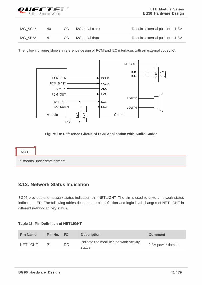
3.11. PCM* and I2C* Interfaces
BG96 provides one Pulse Code Modulation (PCM) digital interface and one I2C interface. The following
table shows the pin definition of the two interfaces which can be applied on audio codec design.
Table 15: Pin Definition of PCM and I2C Interfaces
Pin Name Pin No. I/O Description Comment
PCM_CLK* 4 DO PCM clock output 1.8V power domain
PCM_SYNC* 5 DO PCM frame synchronization
output 1.8V power domain
PCM_IN* 6 DI PCM data input 1.8V power domain
PCM_OUT* 7 DO PCM data output 1.8V power domain
NOTE
LTE Module Series BG96 Hardware Design
BG96_Hardware_Design 41 / 79
The following figure shows a reference design of PCM and I2C interfaces with an external codec IC.
PCM_IN
PCM_SYNC
PCM_CLK
I2C_SCL
I2C_SDA
Module
1.8V
4.7
K
4.7
K
BCLK
WCLK
ADC
SCL
SDA
BIA
S
MICBIAS
INP
INN
LOUTP
LOUTN
Codec
PCM_OUT DAC
Figure 18: Reference Circuit of PCM Application with Audio Codec
“*” means under development.
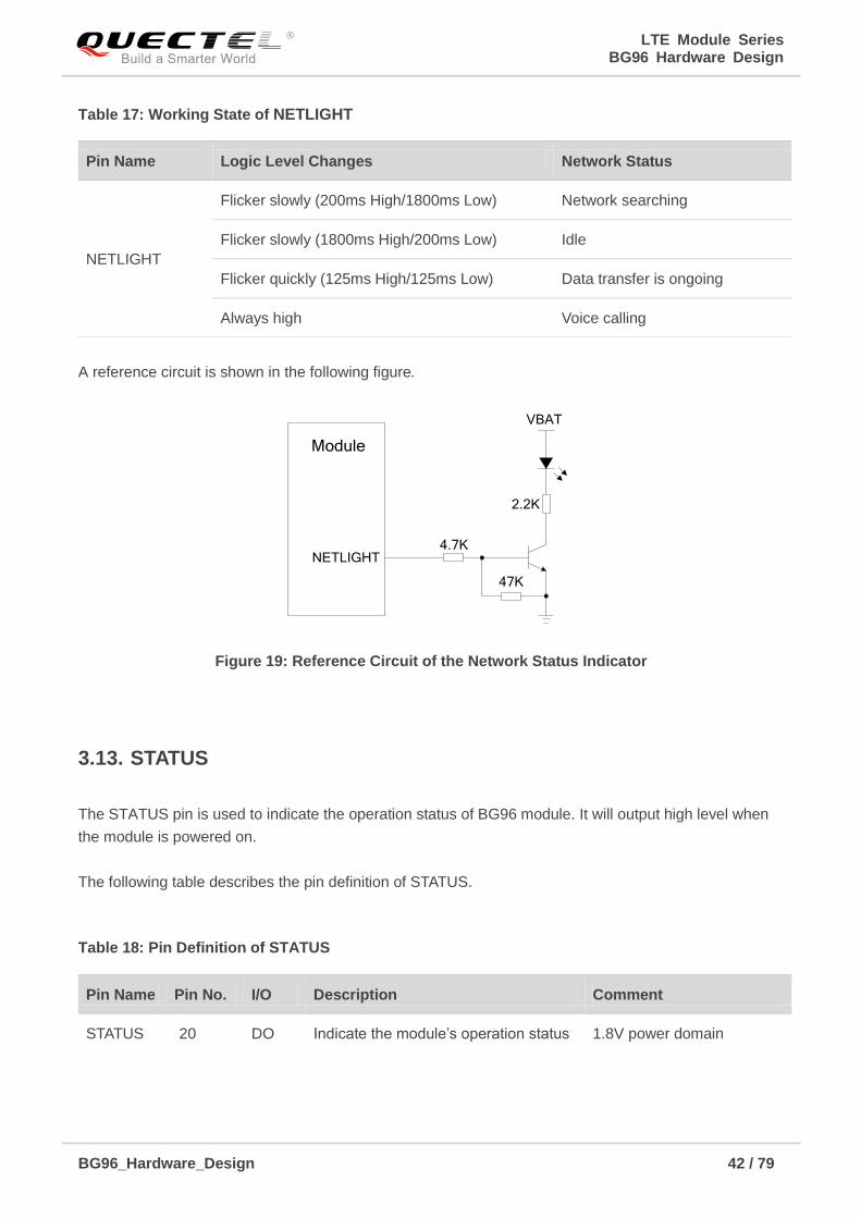
3.12. Network Status Indication
BG96 provides one network status indication pin: NETLIGHT. The pin is used to drive a network status
indication LED. The following tables describe the pin definition and logic level changes of NETLIGHT in
different network activity status.
Table 16: Pin Definition of NETLIGHT
I2C_SCL* 40 OD I2C serial clock Require external pull-up to 1.8V
I2C_SDA* 41 OD I2C serial data Require external pull-up to 1.8V
Pin Name Pin No. I/O Description Comment
NETLIGHT 21 DO Indicate the module’s network activity
status 1.8V power domain
NOTE
LTE Module Series BG96 Hardware Design
BG96_Hardware_Design 42 / 79
Table 17: Working State of NETLIGHT
A reference circuit is shown in the following figure.
4.7K
47K
VBAT
2.2K
Module
NETLIGHT
Figure 19: Reference Circuit of the Network Status Indicator
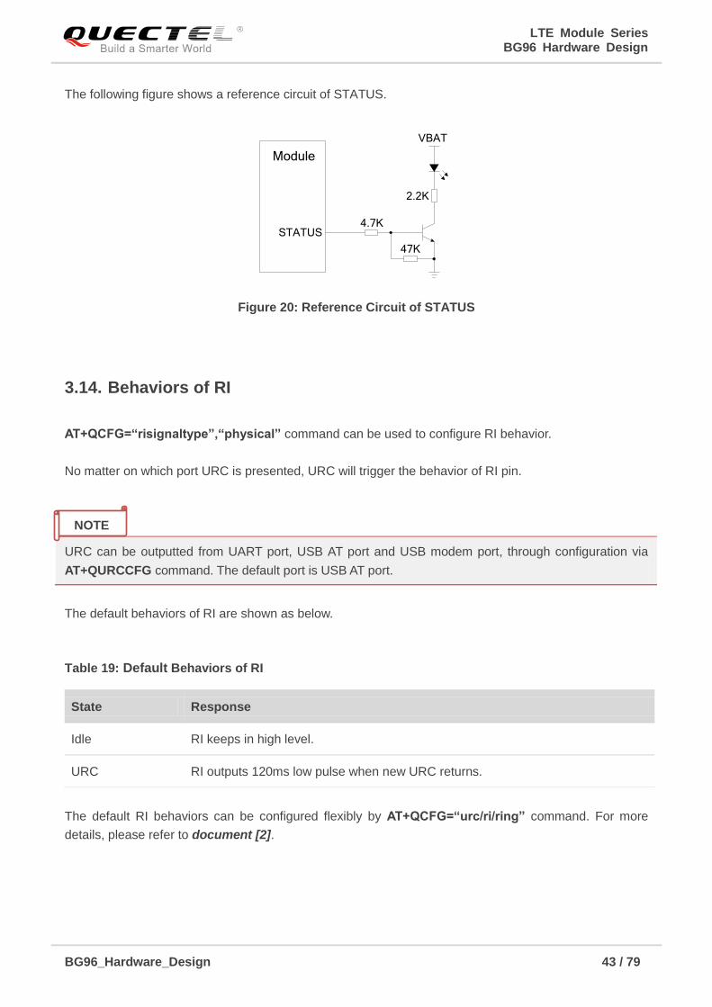
3.13. STATUS
The STATUS pin is used to indicate the operation status of BG96 module. It will output high level when
the module is powered on.
The following table describes the pin definition of STATUS.
Table 18: Pin Definition of STATUS
Pin Name Logic Level Changes Network Status
NETLIGHT
Flicker slowly (200ms High/1800ms Low) Network searching
Flicker slowly (1800ms High/200ms Low) Idle
Flicker quickly (125ms High/125ms Low) Data transfer is ongoing
Always high Voice calling
Pin Name Pin No. I/O Description Comment
STATUS 20 DO Indicate the module’s operation status 1.8V power domain
LTE Module Series BG96 Hardware Design
BG96_Hardware_Design 43 / 79
The following figure shows a reference circuit of STATUS.
4.7K
47K
VBAT
2.2K
Module
STATUS
Figure 20: Reference Circuit of STATUS
3.14. Behaviors of RI
AT+QCFG=“risignaltype”,“physical” command can be used to configure RI behavior.
No matter on which port URC is presented, URC will trigger the behavior of RI pin.
URC can be outputted from UART port, USB AT port and USB modem port, through configuration via
AT+QURCCFG command. The default port is USB AT port.
The default behaviors of RI are shown as below.
Table 19: Default Behaviors of RI
The default RI behaviors can be configured flexibly by AT+QCFG=“urc/ri/ring” command. For more
details, please refer to document [2].
State Response
Idle RI keeps in high level.
URC RI outputs 120ms low pulse when new URC returns.
NOTE
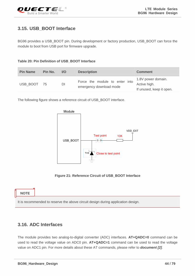
LTE Module Series BG96 Hardware Design
BG96_Hardware_Design 44 / 79
3.15. USB_BOOT Interface
BG96 provides a USB_BOOT pin. During development or factory production, USB_BOOT can force the
module to boot from USB port for firmware upgrade.
Table 20: Pin Definition of USB_BOOT Interface
The following figure shows a reference circuit of USB_BOOT interface.
Module
USB_BOOT
VDD_EXT
10KTest point
TVS Close to test point
Figure 21: Reference Circuit of USB_BOOT Interface
It is recommended to reserve the above circuit design during application design.
3.16. ADC Interfaces
The module provides two analog-to-digital converter (ADC) interfaces. AT+QADC=0 command can be
used to read the voltage value on ADC0 pin. AT+QADC=1 command can be used to read the voltage
value on ADC1 pin. For more details about these AT commands, please refer to document [2].
Pin Name Pin No. I/O Description Comment
USB_BOOT 75 DI Force the module to enter into
emergency download mode
1.8V power domain.
Active high.
If unused, keep it open.
NOTE
LTE Module Series BG96 Hardware Design
BG96_Hardware_Design 45 / 79
In order to improve the accuracy of ADC voltage values, the trace of ADC should be surrounded by
ground.
Table 21: Pin Definition of ADC Interfaces
The following table describes the characteristics of ADC interfaces.
Table 22: Characteristics of ADC Interfaces
1. ADC input voltage must not exceed 1.8V.
2. It is prohibited to supply any voltage to ADC pins when VBAT is removed.
3. It is recommended to use resistor divider circuit for ADC application, and the divider resistor accuracy
should be no less than 1%.
3.17. GPIO Interfaces
The module provides two general-purpose input and output (GPIO) interfaces. AT+QFWD* command can
be used to configure corresponding GPIO pin’s status. For more details about the AT command, please
refer to document [2].
Pin Name Pin No. Description
ADC0 24 General purpose analog to digital converter interface
ADC1 2 General purpose analog to digital converter interface
Parameter Min. Typ. Max. Unit
ADC0 Voltage Range 0.3 1.8 V
ADC1 Voltage Range 0.3 1.8 V
ADC Resolution 15 bits
NOTES
LTE Module Series BG96 Hardware Design
BG96_Hardware_Design 46 / 79
Table 23: Pin Definition of GPIO Interfaces
The following table describes the characteristics of GPIO interfaces.
Table 24: Logic Levels of GPIO interfaces
“*” means under development.
Pin Name Pin No. Description
GPIO26 26 General purpose input and output interface
GPIO64 64 General purpose input and output interface
Parameter Min. Max. Unit
VIL -0.3 0.6 V
VIH 1.2 2.0 V
VOL 0 0.45 V
VOH 1.35 1.8 V
NOTE
LTE Module Series BG96 Hardware Design
BG96_Hardware_Design 47 / 79
4 GNSS Receiver
4.1. General Description
BG96 includes a fully integrated global navigation satellite system solution that supports Gen8C-Lite of
Qualcomm (GPS, GLONASS, BeiDou/Compass, Galileo and QZSS).
BG96 supports standard NMEA-0183 protocol, and outputs NMEA sentences at 1Hz data update rate via
USB interface by default.
By default, BG96 GNSS engine is switched off. It has to be switched on via AT command. For more
details about GNSS engine technology and configurations, please refer to document [3].
4.2. GNSS Performance
The following table shows the GNSS performance of BG96.
Table 25: GNSS Performance
Parameter Description Conditions Typ. Unit
Sensitivity
(GNSS)
Cold start Autonomous -146 dBm
Reacquisition Autonomous -157 dBm
Tracking Autonomous -157 dBm
TTFF
(GNSS)
Cold start
@open sky
Autonomous 31 s
XTRA enabled 11.54 s
Warm start
@open sky
Autonomous 21 s
XTRA enabled 2.52 s
LTE Module Series BG96 Hardware Design
BG96_Hardware_Design 48 / 79
1. Tracking sensitivity: the lowest GNSS signal value at the antenna port on which the module can keep
on positioning for 3 minutes.
2. Reacquisition sensitivity: the lowest GNSS signal value at the antenna port on which the module can
fix position again within 3 minutes after loss of lock.
3. Cold start sensitivity: the lowest GNSS signal value at the antenna port on which the module fixes
position within 3 minutes after executing cold start command.
4.3. Layout Guidelines
The following layout guidelines should be taken into account in customers designs.
Maximize the distance between GNSS antenna and main antenna.
Digital circuits such as (U)SIM card, USB interface, camera module, display connector and SD card
should be kept away from the antennas.
Use ground vias around the GNSS trace and sensitive analog signal traces to provide coplanar
isolation and protection.
Keep 50Ω characteristic impedance for the ANT_GNSS trace.
Please refer to Chapter 5 for GNSS antenna reference design and antenna installation information.
Hot start
@open sky
Autonomous 2.7 s
XTRA enabled 1.82 s
Accuracy
(GNSS) CEP-50
Autonomous
@open sky < 2.5 m
NOTES
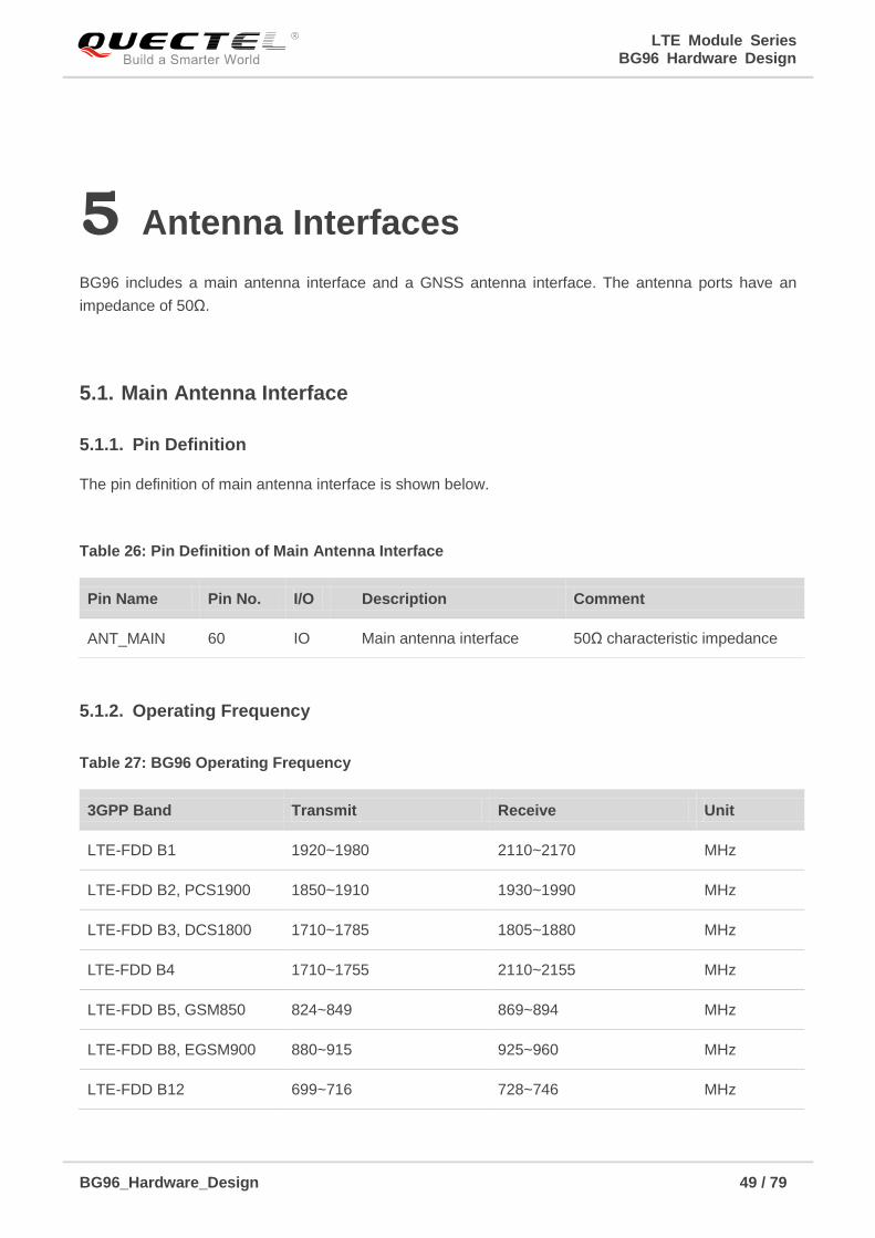
LTE Module Series BG96 Hardware Design
BG96_Hardware_Design 49 / 79
5 Antenna Interfaces
BG96 includes a main antenna interface and a GNSS antenna interface. The antenna ports have an
impedance of 50Ω.
5.1. Main Antenna Interface
5.1.1. Pin Definition
The pin definition of main antenna interface is shown below.
Table 26: Pin Definition of Main Antenna Interface
5.1.2. Operating Frequency
Table 27: BG96 Operating Frequency
Pin Name Pin No. I/O Description Comment
ANT_MAIN 60 IO Main antenna interface 50Ω characteristic impedance
3GPP Band Transmit Receive Unit
LTE-FDD B1 1920~1980 2110~2170 MHz
LTE-FDD B2, PCS1900 1850~1910 1930~1990 MHz
LTE-FDD B3, DCS1800 1710~1785 1805~1880 MHz
LTE-FDD B4 1710~1755 2110~2155 MHz
LTE-FDD B5, GSM850 824~849 869~894 MHz
LTE-FDD B8, EGSM900 880~915 925~960 MHz
LTE-FDD B12 699~716 728~746 MHz
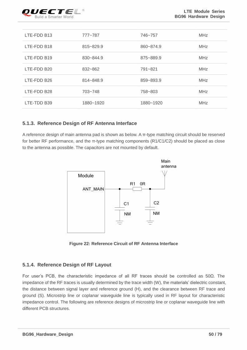
LTE Module Series BG96 Hardware Design
BG96_Hardware_Design 50 / 79
5.1.3. Reference Design of RF Antenna Interface
A reference design of main antenna pad is shown as below. A π-type matching circuit should be reserved
for better RF performance, and the π-type matching components (R1/C1/C2) should be placed as close
to the antenna as possible. The capacitors are not mounted by default.
ANT_MAIN
R1 0R
C1
Module
Main
antenna
NM
C2
NM
Figure 22: Reference Circuit of RF Antenna Interface
5.1.4. Reference Design of RF Layout
For user’s PCB, the characteristic impedance of all RF traces should be controlled as 50Ω. The
impedance of the RF traces is usually determined by the trace width (W), the materials’ dielectric constant,
the distance between signal layer and reference ground (H), and the clearance between RF trace and
ground (S). Microstrip line or coplanar waveguide line is typically used in RF layout for characteristic
impedance control. The following are reference designs of microstrip line or coplanar waveguide line with
different PCB structures.
LTE-FDD B13 777~787 746~757 MHz
LTE-FDD B18 815~829.9 860~874.9 MHz
LTE-FDD B19 830~844.9 875~889.9 MHz
LTE-FDD B20 832~862 791~821 MHz
LTE-FDD B26 814~848.9 859~893.9 MHz
LTE-FDD B28 703~748 758~803 MHz
LTE-TDD B39 1880~1920 1880~1920 MHz
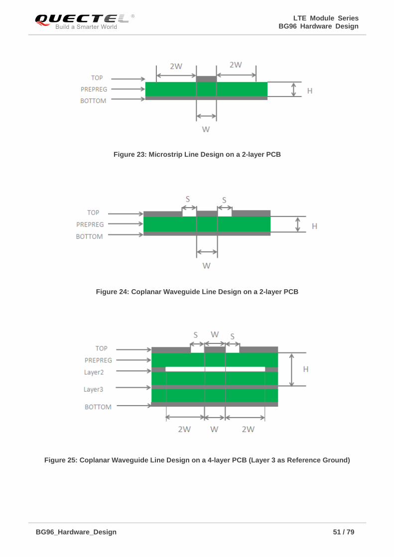
LTE Module Series BG96 Hardware Design
BG96_Hardware_Design 51 / 79
Figure 23: Microstrip Line Design on a 2-layer PCB
Figure 24: Coplanar Waveguide Line Design on a 2-layer PCB
Figure 25: Coplanar Waveguide Line Design on a 4-layer PCB (Layer 3 as Reference Ground)
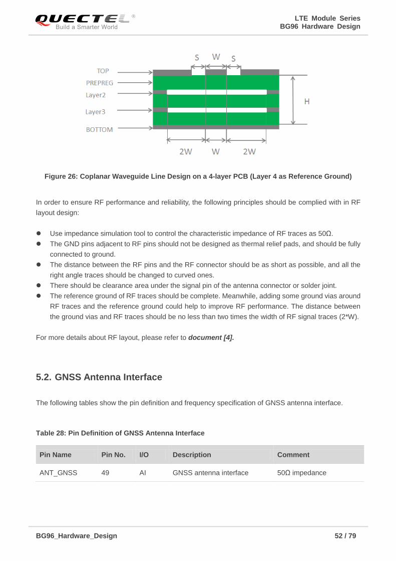
LTE Module Series BG96 Hardware Design
BG96_Hardware_Design 52 / 79
Figure 26: Coplanar Waveguide Line Design on a 4-layer PCB (Layer 4 as Reference Ground)
In order to ensure RF performance and reliability, the following principles should be complied with in RF
layout design:
Use impedance simulation tool to control the characteristic impedance of RF traces as 50Ω.
The GND pins adjacent to RF pins should not be designed as thermal relief pads, and should be fully
connected to ground.
The distance between the RF pins and the RF connector should be as short as possible, and all the
right angle traces should be changed to curved ones.
There should be clearance area under the signal pin of the antenna connector or solder joint.
The reference ground of RF traces should be complete. Meanwhile, adding some ground vias around
RF traces and the reference ground could help to improve RF performance. The distance between
the ground vias and RF traces should be no less than two times the width of RF signal traces (2*W).
For more details about RF layout, please refer to document [4].
5.2. GNSS Antenna Interface
The following tables show the pin definition and frequency specification of GNSS antenna interface.
Table 28: Pin Definition of GNSS Antenna Interface
Pin Name Pin No. I/O Description Comment
ANT_GNSS 49 AI GNSS antenna interface 50Ω impedance
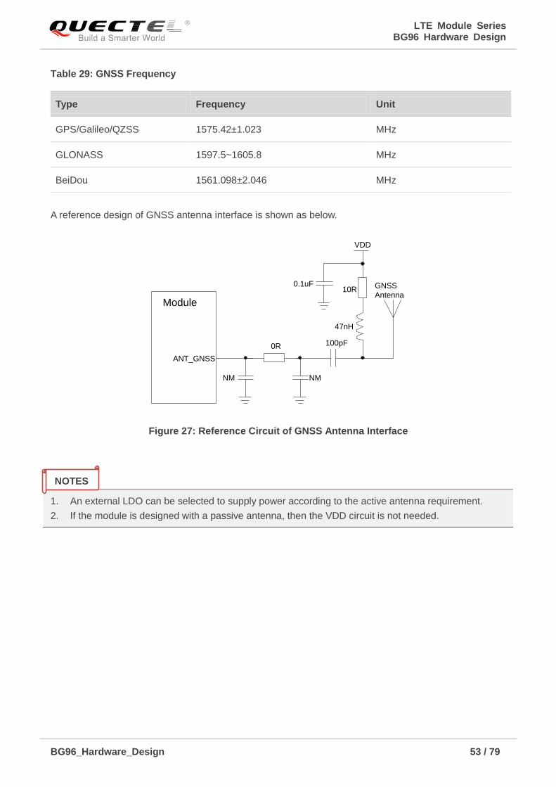
LTE Module Series BG96 Hardware Design
BG96_Hardware_Design 53 / 79
Table 29: GNSS Frequency
A reference design of GNSS antenna interface is shown as below.
GNSS
Antenna
VDD
Module
ANT_GNSS
47nH
10R0.1uF
0R
NM NM
100pF
Figure 27: Reference Circuit of GNSS Antenna Interface
1. An external LDO can be selected to supply power according to the active antenna requirement.
2. If the module is designed with a passive antenna, then the VDD circuit is not needed.
Type Frequency Unit
GPS/Galileo/QZSS 1575.42±1.023 MHz
GLONASS 1597.5~1605.8 MHz
BeiDou 1561.098±2.046 MHz
NOTES
LTE Module Series BG96 Hardware Design
BG96_Hardware_Design 54 / 79
5.3. Antenna Installation
5.3.1. Antenna Requirements
The following table shows the requirements on main antenna and GNSS antenna.
Table 30: Antenna Requirements
1) It is recommended to use a passive GNSS antenna when LTE B13 or B14 is supported, as the use of
active antenna may generate harmonics which will affect the GNSS performance.
5.3.2. Recommended RF Connector for Antenna Installation
If RF connector is used for antenna connection, it is recommended to use the U.FL-R-SMT connector
provided by HIROSE.
Antenna Type Requirements
GNSS 1)
Frequency range: 1559MHz ~1609MHz
Polarization: RHCP or linear
VSWR: < 2 (Typ.)
Passive antenna gain: > 0dBi
Active antenna noise figure: < 1.5dB
Active antenna gain: > 0dBi
Active antenna embedded LNA gain: < 17dB
LTE/GSM
VSWR: ≤ 2
Efficiency: > 30%
Max Input Power (W): 50
Input Impedance (Ω): 50
Cable Insertion Loss: < 1dB
(LTE B5/B8/B12/B13/B18/B19/B20/B26/B28, GSM850/EGSM900)
Cable Insertion Loss: < 1.5dB
(LTE B1/B2/B3/B4/B39, DCS1800/PCS1900)
NOTE
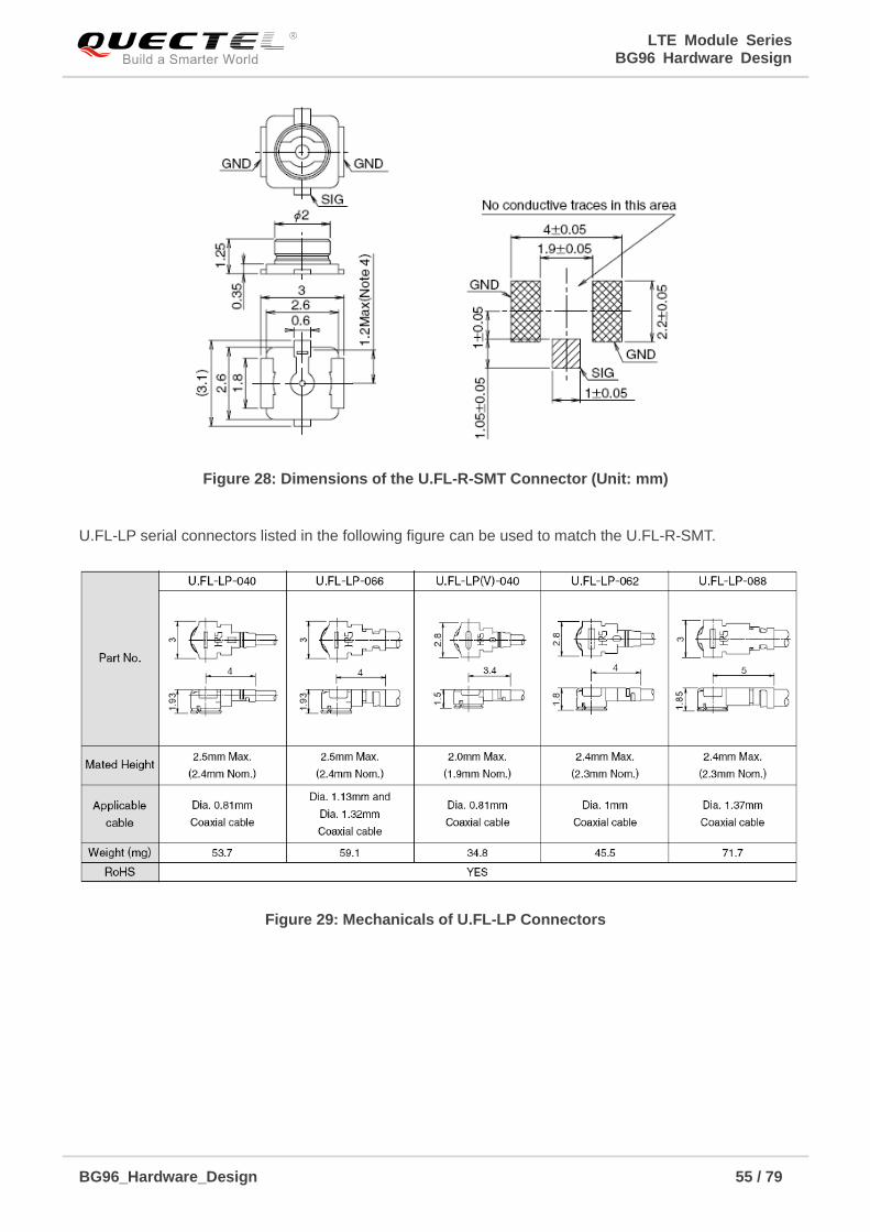
LTE Module Series BG96 Hardware Design
BG96_Hardware_Design 55 / 79
Figure 28: Dimensions of the U.FL-R-SMT Connector (Unit: mm)
U.FL-LP serial connectors listed in the following figure can be used to match the U.FL-R-SMT.
Figure 29: Mechanicals of U.FL-LP Connectors
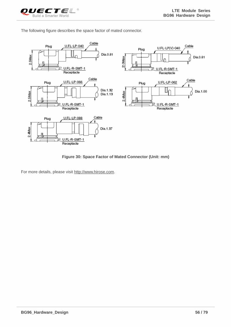
LTE Module Series BG96 Hardware Design
BG96_Hardware_Design 56 / 79
The following figure describes the space factor of mated connector.
Figure 30: Space Factor of Mated Connector (Unit: mm)
For more details, please visit http://www.hirose.com.
LTE Module Series BG96 Hardware Design
BG96_Hardware_Design 57 / 79
6 Electrical, Reliability and Radio
Characteristics
6.1. Absolute Maximum Ratings
Absolute maximum ratings for power supply and voltage on digital and analog pins of the module are
listed in the following table.
Table 31: Absolute Maximum Ratings
6.2. Power Supply Ratings
Table 32: Power Supply Ratings
Parameter Min. Max. Unit
VBAT_BB -0.5 6 V
VBAT_RF -1.2 6 V
USB_VBUS -0.3 5.5 V
Voltage at Digital Pins -0.3 2.3 V
Parameter Description Conditions Min. Typ. Max. Unit
VBAT VBAT_BB and VBAT_RF
The actual input voltages
must stay between the
minimum and maximum
values.
3.3 3.8 4.3 V
IVBAT Peak supply current
(during transmission slot)
Maximum power control
level on EGSM900 1.8 2.0 A
LTE Module Series BG96 Hardware Design
BG96_Hardware_Design 58 / 79
6.3. Operation and Storage Temperatures
The operation and storage temperatures of the module are listed in the following table.
Table 33: Operation and Storage Temperatures
1. 1)
Within operation temperature range, the module is 3GPP compliant.
2. 2)
Within extended temperature range, the module remains the ability to establish and maintain a
voice, SMS, data transmission, emergency call, etc. There is no unrecoverable malfunction. There
are also no effects on radio spectrum and no harm to radio network. Only one or more parameters
like Pout might reduce in their value and exceed the specified tolerances. When the temperature
returns to the normal operating temperature levels, the module will meet 3GPP specifications again.
6.4. Current Consumption
The following table shows current consumption of BG96 module.
Table 34: BG96 Current Consumption
USB_VBUS USB detection 3.0 5.0 5.25 V
Parameter Min. Typ. Max. Unit
Operation Temperature Range 1)
-35 +25 +75 ºC
Extended Temperature Range 2)
-40 +85 ºC
Storage Temperature Range -40 +90 ºC
Parameter Description Conditions Typ. Unit
IVBAT
OFF State Power down 8 uA
PSM Power Saving Mode @Real Network 10 uA
NOTES
LTE Module Series BG96 Hardware Design
BG96_Hardware_Design 59 / 79
Quiescent
Current AT+CFUN=0 @Sleep State 0.8
1) mA
Sleep State
DRX=1.28s @Real LTE Cat M1 Network 1.7 2)
mA
DRX=1.28s @Real LTE Cat NB1 Network 2.3 2)
mA
e-I-DRX=20.48s @Real LTE Cat M1 Network 1.1 2)
mA
e-I-DRX=20.48s @Real LTE Cat NB1 Network 1.7 2)
mA
@Real 2G Network 2.0 2)
mA
Idle State
DRX=1.28s @Real LTE Cat M1 Network 16 3)
mA
DRX=1.28s @Real LTE Cat NB1 Network 16 3)
mA
e-I-DRX=20.48s @Real LTE Cat M1 Network 15 3)
mA
e-I-DRX=20.48s @Real LTE Cat NB1 Network 15 3)
mA
@Real 2G Network 15 3)
mA
LTE Cat M1
data transfer
(GNSS OFF)
LTE-FDD B1 @23.31dBm 220 mA
LTE-FDD B2 @23.05dBm 208 mA
LTE-FDD B3 @23.09dBm 214 mA
LTE-FDD B4 @23.19dBm 214 mA
LTE-FDD B5 @23.22dBm 210 mA
LTE-FDD B8 @21.83dBm 203 mA
LTE-FDD B12 @21.88dBm 215 mA
LTE-FDD B13 @21.96dBm 197 mA
LTE-FDD B18 @23.04dBm 212 mA
LTE-FDD B19 @23.13dBm 211 mA
LTE-FDD B20 @23.07dBm 209 mA
LTE-FDD B26 @22.81dBm 214 mA
LTE-FDD B28 @22.52dBm 215 mA
LTE-TDD B39 @TBD TBD mA
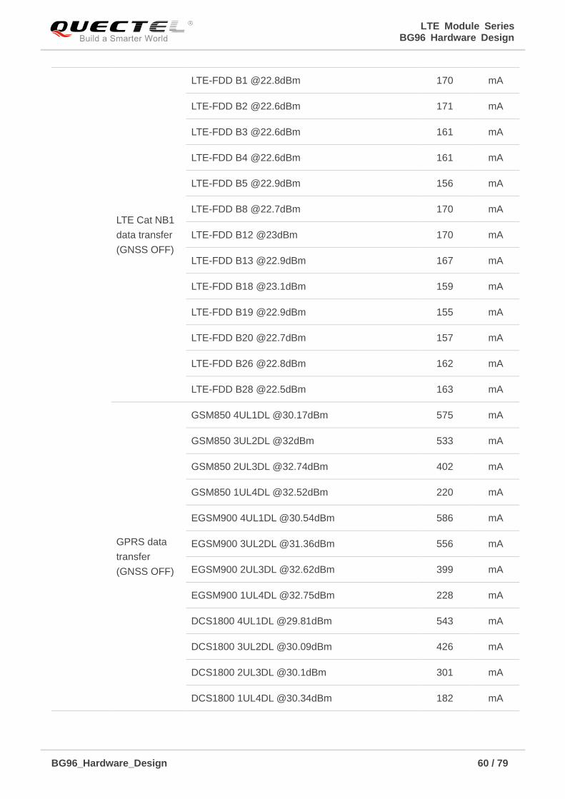
LTE Module Series BG96 Hardware Design
BG96_Hardware_Design 60 / 79
LTE Cat NB1
data transfer
(GNSS OFF)
LTE-FDD B1 @22.8dBm 170 mA
LTE-FDD B2 @22.6dBm 171 mA
LTE-FDD B3 @22.6dBm 161 mA
LTE-FDD B4 @22.6dBm 161 mA
LTE-FDD B5 @22.9dBm 156 mA
LTE-FDD B8 @22.7dBm 170 mA
LTE-FDD B12 @23dBm 170 mA
LTE-FDD B13 @22.9dBm 167 mA
LTE-FDD B18 @23.1dBm 159 mA
LTE-FDD B19 @22.9dBm 155 mA
LTE-FDD B20 @22.7dBm 157 mA
LTE-FDD B26 @22.8dBm 162 mA
LTE-FDD B28 @22.5dBm 163 mA
GPRS data
transfer
(GNSS OFF)
GSM850 4UL1DL @30.17dBm 575 mA
GSM850 3UL2DL @32dBm 533 mA
GSM850 2UL3DL @32.74dBm 402 mA
GSM850 1UL4DL @32.52dBm 220 mA
EGSM900 4UL1DL @30.54dBm 586 mA
EGSM900 3UL2DL @31.36dBm 556 mA
EGSM900 2UL3DL @32.62dBm 399 mA
EGSM900 1UL4DL @32.75dBm 228 mA
DCS1800 4UL1DL @29.81dBm 543 mA
DCS1800 3UL2DL @30.09dBm 426 mA
DCS1800 2UL3DL @30.1dBm 301 mA
DCS1800 1UL4DL @30.34dBm 182 mA
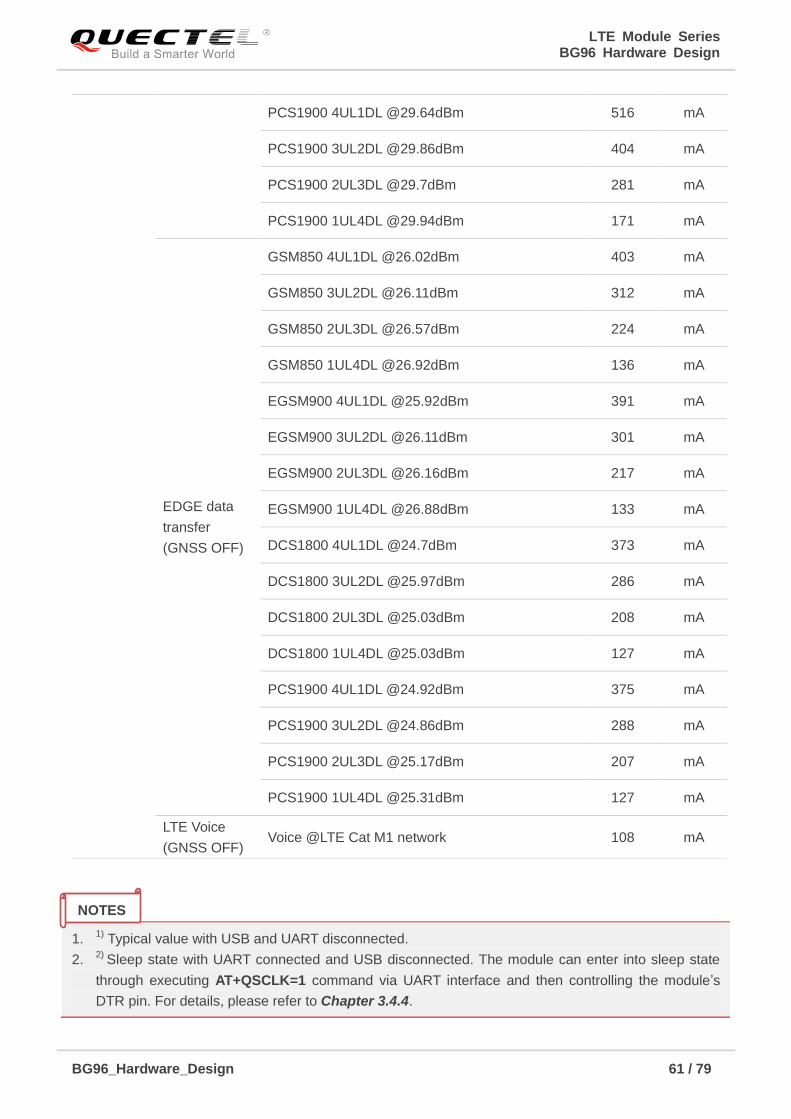
LTE Module Series BG96 Hardware Design
BG96_Hardware_Design 61 / 79
1. 1)
Typical value with USB and UART disconnected.
2. 2)
Sleep state with UART connected and USB disconnected. The module can enter into sleep state
through executing AT+QSCLK=1 command via UART interface and then controlling the module’s
DTR pin. For details, please refer to Chapter 3.4.4.
PCS1900 4UL1DL @29.64dBm 516 mA
PCS1900 3UL2DL @29.86dBm 404 mA
PCS1900 2UL3DL @29.7dBm 281 mA
PCS1900 1UL4DL @29.94dBm 171 mA
EDGE data
transfer
(GNSS OFF)
GSM850 4UL1DL @26.02dBm 403 mA
GSM850 3UL2DL @26.11dBm 312 mA
GSM850 2UL3DL @26.57dBm 224 mA
GSM850 1UL4DL @26.92dBm 136 mA
EGSM900 4UL1DL @25.92dBm 391 mA
EGSM900 3UL2DL @26.11dBm 301 mA
EGSM900 2UL3DL @26.16dBm 217 mA
EGSM900 1UL4DL @26.88dBm 133 mA
DCS1800 4UL1DL @24.7dBm 373 mA
DCS1800 3UL2DL @25.97dBm 286 mA
DCS1800 2UL3DL @25.03dBm 208 mA
DCS1800 1UL4DL @25.03dBm 127 mA
PCS1900 4UL1DL @24.92dBm 375 mA
PCS1900 3UL2DL @24.86dBm 288 mA
PCS1900 2UL3DL @25.17dBm 207 mA
PCS1900 1UL4DL @25.31dBm 127 mA
LTE Voice
(GNSS OFF) Voice @LTE Cat M1 network 108 mA
NOTES
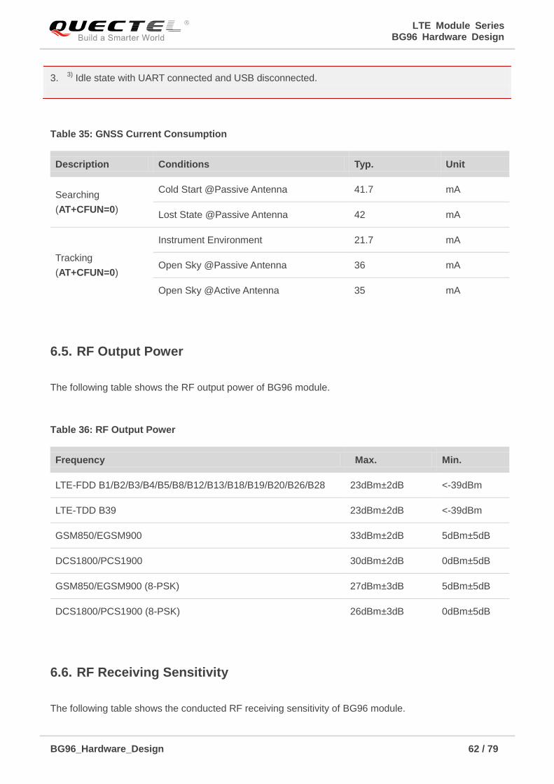
LTE Module Series BG96 Hardware Design
BG96_Hardware_Design 62 / 79
3. 3)
Idle state with UART connected and USB disconnected.
Table 35: GNSS Current Consumption
6.5. RF Output Power
The following table shows the RF output power of BG96 module.
Table 36: RF Output Power
6.6. RF Receiving Sensitivity
The following table shows the conducted RF receiving sensitivity of BG96 module.
Description Conditions Typ. Unit
Searching
(AT+CFUN=0)
Cold Start @Passive Antenna 41.7 mA
Lost State @Passive Antenna 42 mA
Tracking
(AT+CFUN=0)
Instrument Environment 21.7 mA
Open Sky @Passive Antenna 36 mA
Open Sky @Active Antenna 35 mA
Frequency Max. Min.
LTE-FDD B1/B2/B3/B4/B5/B8/B12/B13/B18/B19/B20/B26/B28 23dBm±2dB <-39dBm
LTE-TDD B39 23dBm±2dB <-39dBm
GSM850/EGSM900 33dBm±2dB 5dBm±5dB
DCS1800/PCS1900 30dBm±2dB 0dBm±5dB
GSM850/EGSM900 (8-PSK) 27dBm±3dB 5dBm±5dB
DCS1800/PCS1900 (8-PSK) 26dBm±3dB 0dBm±5dB
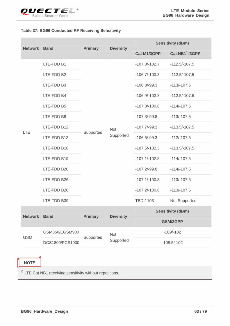
LTE Module Series BG96 Hardware Design
BG96_Hardware_Design 63 / 79
Table 37: BG96 Conducted RF Receiving Sensitivity
1) LTE Cat NB1 receiving sensitivity without repetitions.
Network Band Primary Diversity
Sensitivity (dBm)
Cat M1/3GPP Cat NB11)
/3GPP
LTE
LTE-FDD B1
Supported Not
Supported
-107.0/-102.7 -112.5/-107.5
LTE-FDD B2 -106.7/-100.3 -112.5/-107.5
LTE-FDD B3 -106.8/-99.3 -113/-107.5
LTE-FDD B4 -106.9/-102.3 -112.5/-107.5
LTE-FDD B5 -107.0/-100.8 -114/-107.5
LTE-FDD B8 -107.3/-99.8 -113/-107.5
LTE-FDD B12 -107.7/-99.3 -113.5/-107.5
LTE-FDD B13 -106.5/-99.3 -112/-107.5
LTE-FDD B18 -107.5/-102.3 -113.5/-107.5
LTE-FDD B19 -107.1/-102.3 -114/-107.5
LTE-FDD B20 -107.2/-99.8 -114/-107.5
LTE-FDD B26 -107.1/-100.3 -113/-107.5
LTE-FDD B28 -107.2/-100.8 -113/-107.5
LTE-TDD B39 TBD /-103 Not Supported
Network Band Primary Diversity
Sensitivity (dBm)
GSM/3GPP
GSM
GSM850/EGSM900
Supported Not
Supported
-109/-102
DCS1800/PCS1900 -108.5/-102
NOTE
LTE Module Series BG96 Hardware Design
BG96_Hardware_Design 64 / 79
6.7. Electrostatic Discharge
The module is not protected against electrostatics discharge (ESD) in general. Consequently, it is subject
to ESD handling precautions that typically apply to ESD sensitive components. Proper ESD handling and
packaging procedures must be applied throughout the processing, handling and operation of any
application that incorporates the module.
The following table shows the electrostatic discharge characteristics of BG96 module.
Table 38: Electrostatic Discharge Characteristics
Tested Points Contact Discharge Air Discharge Unit
VBAT, GND ±10 ±15 kV
Main/GNSS Antenna
Interfaces ±10 ±15 kV
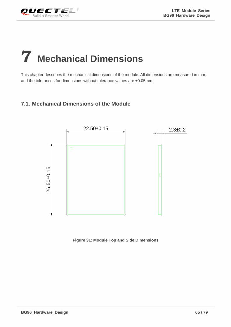
LTE Module Series BG96 Hardware Design
BG96_Hardware_Design 65 / 79
7 Mechanical Dimensions
This chapter describes the mechanical dimensions of the module. All dimensions are measured in mm,
and the tolerances for dimensions without tolerance values are ±0.05mm.
7.1. Mechanical Dimensions of the Module
22.50±0.15 2.3±0.2
26
.50±0.1
5
Figure 31: Module Top and Side Dimensions
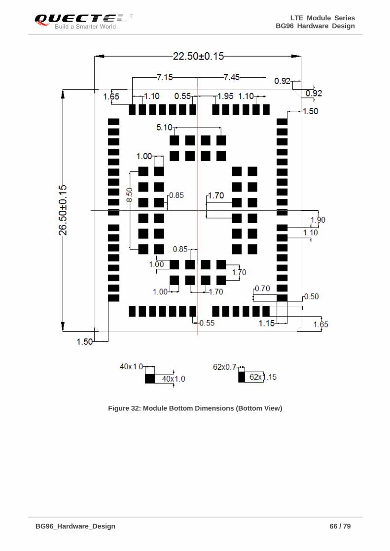
LTE Module Series BG96 Hardware Design
BG96_Hardware_Design 66 / 79
Figure 32: Module Bottom Dimensions (Bottom View)
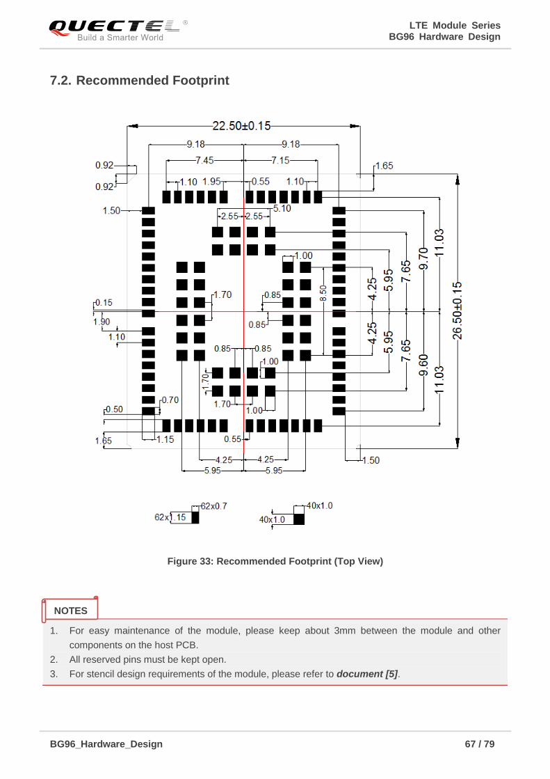
LTE Module Series BG96 Hardware Design
BG96_Hardware_Design 67 / 79
7.2. Recommended Footprint
Figure 33: Recommended Footprint (Top View)
1. For easy maintenance of the module, please keep about 3mm between the module and other
components on the host PCB.
2. All reserved pins must be kept open.
3. For stencil design requirements of the module, please refer to document [5].
NOTES
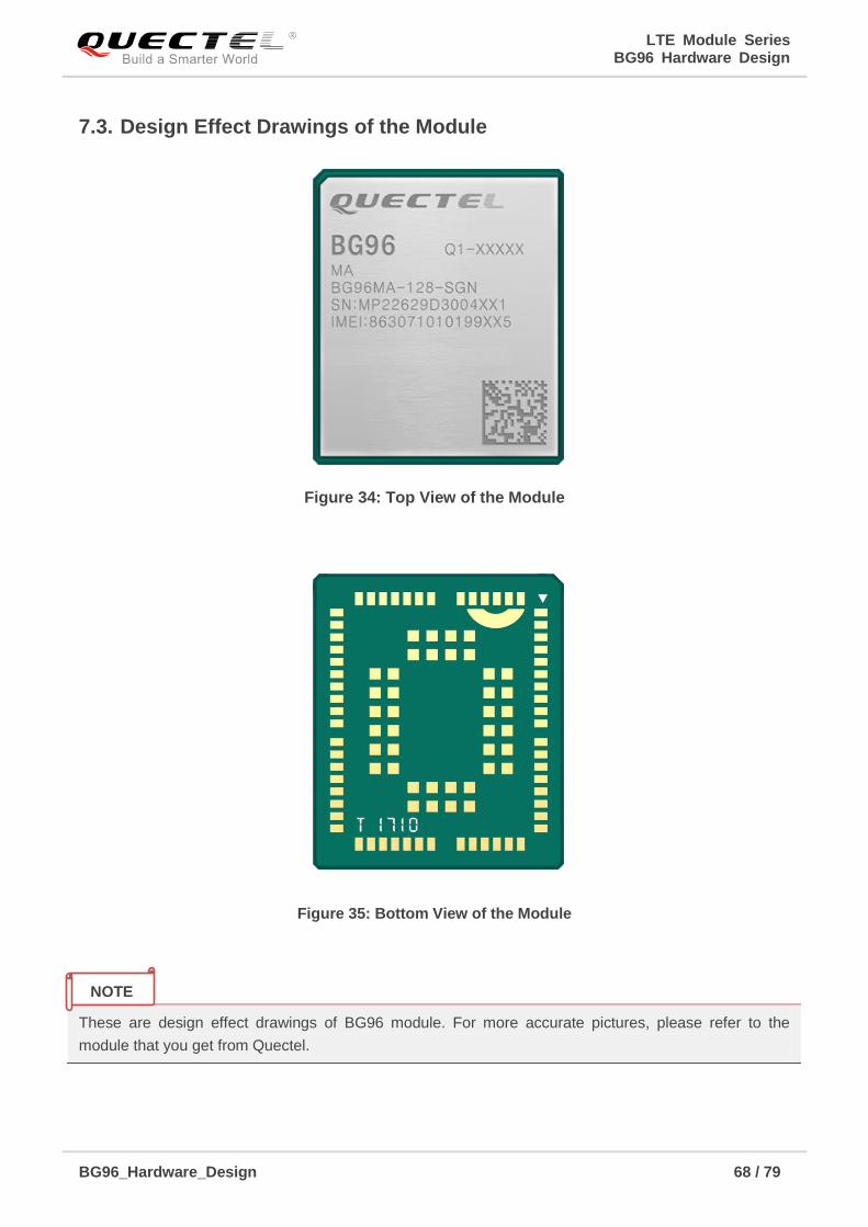
LTE Module Series BG96 Hardware Design
BG96_Hardware_Design 68 / 79
7.3. Design Effect Drawings of the Module
Figure 34: Top View of the Module
Figure 35: Bottom View of the Module
These are design effect drawings of BG96 module. For more accurate pictures, please refer to the
module that you get from Quectel.
NOTE
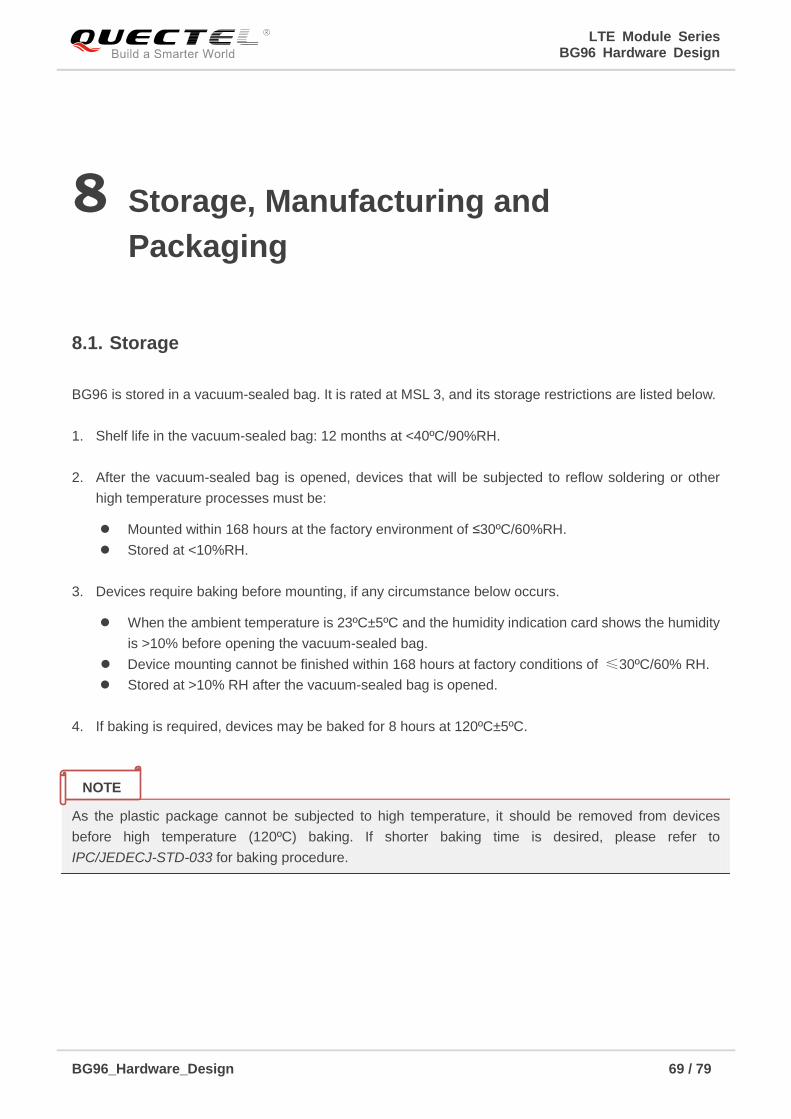
LTE Module Series BG96 Hardware Design
BG96_Hardware_Design 69 / 79
8 Storage, Manufacturing and
Packaging
8.1. Storage
BG96 is stored in a vacuum-sealed bag. It is rated at MSL 3, and its storage restrictions are listed below.
1. Shelf life in the vacuum-sealed bag: 12 months at <40ºC/90%RH.
2. After the vacuum-sealed bag is opened, devices that will be subjected to reflow soldering or other
high temperature processes must be:
Mounted within 168 hours at the factory environment of ≤30ºC/60%RH.
Stored at <10%RH.
3. Devices require baking before mounting, if any circumstance below occurs.
When the ambient temperature is 23ºC±5ºC and the humidity indication card shows the humidity
is >10% before opening the vacuum-sealed bag.
Device mounting cannot be finished within 168 hours at factory conditions of ≤30ºC/60% RH.
Stored at >10% RH after the vacuum-sealed bag is opened.
4. If baking is required, devices may be baked for 8 hours at 120ºC±5ºC.
As the plastic package cannot be subjected to high temperature, it should be removed from devices
before high temperature (120ºC) baking. If shorter baking time is desired, please refer to
IPC/JEDECJ-STD-033 for baking procedure.
NOTE
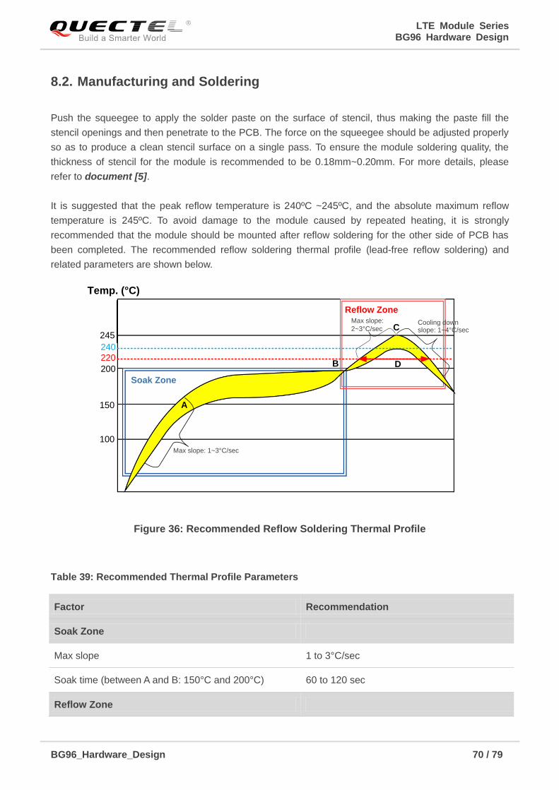
LTE Module Series BG96 Hardware Design
BG96_Hardware_Design 70 / 79
8.2. Manufacturing and Soldering
Push the squeegee to apply the solder paste on the surface of stencil, thus making the paste fill the
stencil openings and then penetrate to the PCB. The force on the squeegee should be adjusted properly
so as to produce a clean stencil surface on a single pass. To ensure the module soldering quality, the
thickness of stencil for the module is recommended to be 0.18mm~0.20mm. For more details, please
refer to document [5].
It is suggested that the peak reflow temperature is 240ºC ~245ºC, and the absolute maximum reflow
temperature is 245ºC. To avoid damage to the module caused by repeated heating, it is strongly
recommended that the module should be mounted after reflow soldering for the other side of PCB has
been completed. The recommended reflow soldering thermal profile (lead-free reflow soldering) and
related parameters are shown below.
Temp. (°C)
Reflow Zone
Soak Zone
245
200
220
240
C
DB
A150
100
Max slope: 1~3°C/sec
Cooling down slope: 1~4°C/sec
Max slope:
2~3°C/sec
Figure 36: Recommended Reflow Soldering Thermal Profile
Table 39: Recommended Thermal Profile Parameters
Factor Recommendation
Soak Zone
Max slope 1 to 3°C/sec
Soak time (between A and B: 150°C and 200°C) 60 to 120 sec
Reflow Zone
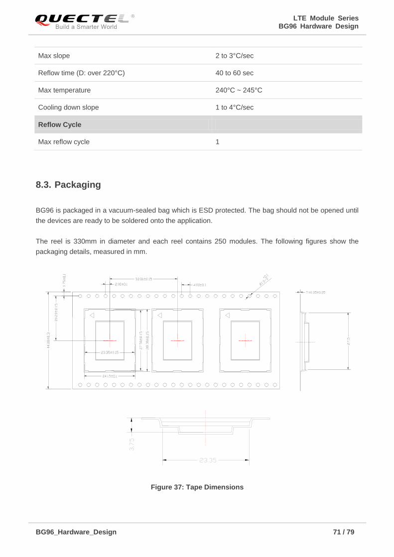
LTE Module Series BG96 Hardware Design
BG96_Hardware_Design 71 / 79
8.3. Packaging
BG96 is packaged in a vacuum-sealed bag which is ESD protected. The bag should not be opened until
the devices are ready to be soldered onto the application.
The reel is 330mm in diameter and each reel contains 250 modules. The following figures show the
packaging details, measured in mm.
Figure 37: Tape Dimensions
Max slope 2 to 3°C/sec
Reflow time (D: over 220°C) 40 to 60 sec
Max temperature 240°C ~ 245°C
Cooling down slope 1 to 4°C/sec
Reflow Cycle
Max reflow cycle 1
LTE Module Series BG96 Hardware Design
BG96_Hardware_Design 72 / 79
Direction of feed
Cover tape
13
10
0
44.5+0.20-0.00
48.5
Figure 38: Reel Dimensions
Table 40: Reel Packaging
Model Name MOQ for MP Minimum Package: 250pcs Minimum Package x 4=1000pcs
BG96 250pcs
Size: 370mm × 350mm × 56mm
N.W: 0.78kg
G.W: 1.46kg
Size: 380mm × 250mm × 365mm
N.W: 3.1kg
G.W: 6.45kg
LTE Module Series BG96 Hardware Design
BG96_Hardware_Design 73 / 79
9 Appendix A References
Table 41: Related Documents
Table 42: Terms and Abbreviations
SN Document Name Remark
[1] Quectel_UMTS<E_EVB_User_Guide UMTS<E EVB User Guide
[2] Quectel_BG96_AT_Commands_Manual BG96 AT Commands Manual
[3] Quectel_BG96_GNSS_AT_Commands_Manual BG96 GNSS AT Commands Manual
[4] Quectel_RF_Layout_Application_Note RF Layout Application Note
[5] Quectel_Module_Secondary_SMT_User_Guide Module Secondary SMT User Guide
Abbreviation Description
AMR Adaptive Multi-rate
bps Bits Per Second
CHAP Challenge Handshake Authentication Protocol
CS Coding Scheme
CTS Clear To Send
DFOTA Delta Firmware Upgrade Over The Air
DL Downlink
DTR Data Terminal Ready
DTX Discontinuous Transmission
e-I-DRX Extended Idle Mode Discontinuous Reception
EPC Evolved Packet Core
LTE Module Series BG96 Hardware Design
BG96_Hardware_Design 74 / 79
ESD Electrostatic Discharge
FDD Frequency Division Duplex
FR Full Rate
GMSK Gaussian Minimum Shift Keying
GSM Global System for Mobile Communications
HSS Home Subscriber Server
I/O Input/Output
Inorm Normal Current
LED Light Emitting Diode
LNA Low Noise Amplifier
LTE Long Term Evolution
MO Mobile Originated
MS Mobile Station (GSM engine)
MT Mobile Terminated
PAP Password Authentication Protocol
PCB Printed Circuit Board
PDU Protocol Data Unit
PPP Point-to-Point Protocol
PSM Power Saving Mode
RF Radio Frequency
RHCP Right Hand Circularly Polarized
Rx Receive
SISO Single Input Single Output
SMS Short Message Service
TDD Time Division Duplexing
LTE Module Series BG96 Hardware Design
BG96_Hardware_Design 75 / 79
TX Transmitting Direction
UL Uplink
UE User Equipment
URC Unsolicited Result Code
(U)SIM (Universal) Subscriber Identity Module
Vmax Maximum Voltage Value
Vnorm Normal Voltage Value
Vmin Minimum Voltage Value
VIHmax Maximum Input High Level Voltage Value
VIHmin Minimum Input High Level Voltage Value
VILmax Maximum Input Low Level Voltage Value
VILmin Minimum Input Low Level Voltage Value
VImax Absolute Maximum Input Voltage Value
VImin Absolute Minimum Input Voltage Value
VOHmax Maximum Output High Level Voltage Value
VOHmin Minimum Output High Level Voltage Value
VOLmax Maximum Output Low Level Voltage Value
VOLmin Minimum Output Low Level Voltage Value
VSWR Voltage Standing Wave Ratio
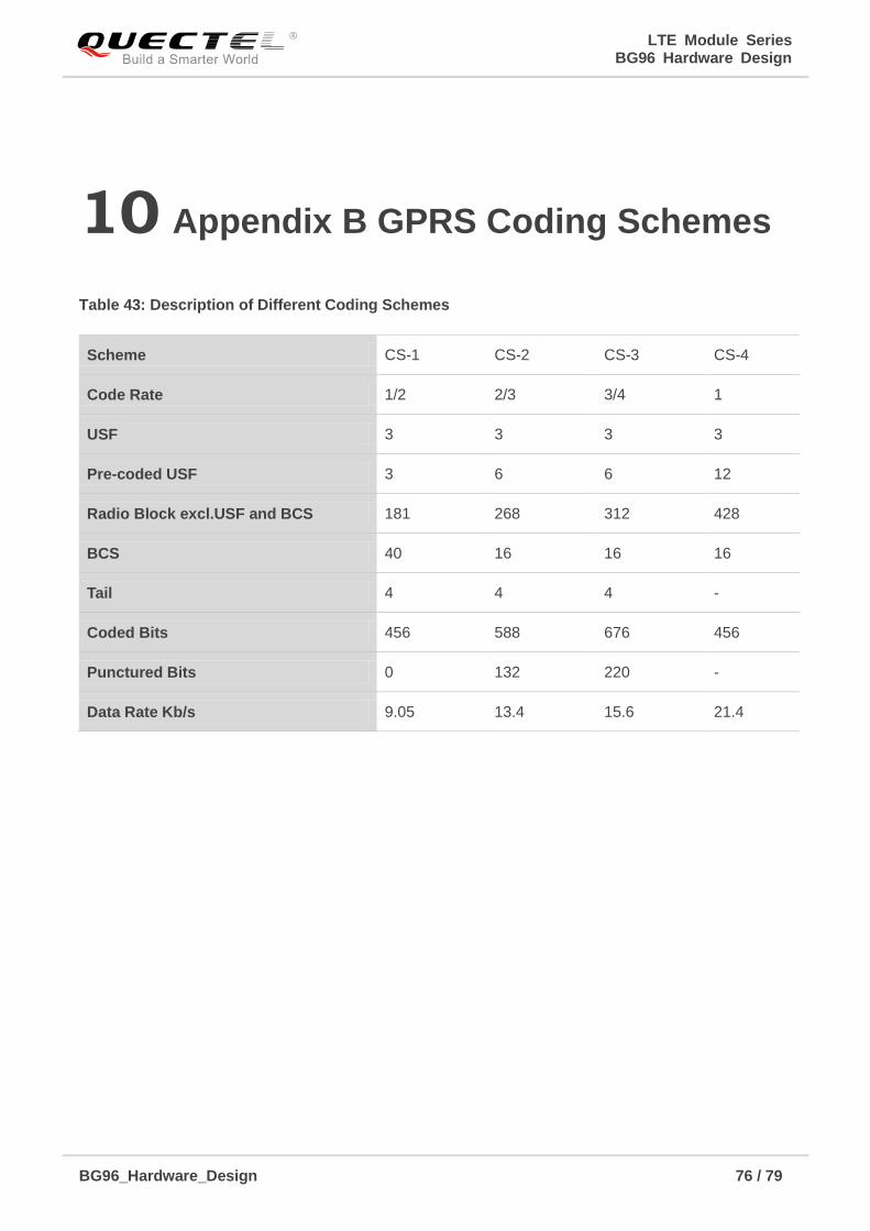
LTE Module Series BG96 Hardware Design
BG96_Hardware_Design 76 / 79
10 Appendix B GPRS Coding Schemes
Table 43: Description of Different Coding Schemes
Scheme CS-1 CS-2 CS-3 CS-4
Code Rate 1/2 2/3 3/4 1
USF 3 3 3 3
Pre-coded USF 3 6 6 12
Radio Block excl.USF and BCS 181 268 312 428
BCS 40 16 16 16
Tail 4 4 4 -
Coded Bits 456 588 676 456
Punctured Bits 0 132 220 -
Data Rate Kb/s 9.05 13.4 15.6 21.4
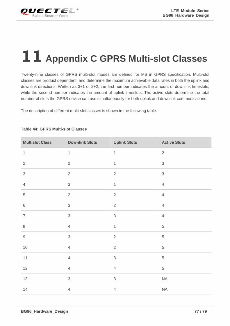
LTE Module Series BG96 Hardware Design
BG96_Hardware_Design 77 / 79
11 Appendix C GPRS Multi-slot Classes
Twenty-nine classes of GPRS multi-slot modes are defined for MS in GPRS specification. Multi-slot
classes are product dependent, and determine the maximum achievable data rates in both the uplink and
downlink directions. Written as 3+1 or 2+2, the first number indicates the amount of downlink timeslots,
while the second number indicates the amount of uplink timeslots. The active slots determine the total
number of slots the GPRS device can use simultaneously for both uplink and downlink communications.
The description of different multi-slot classes is shown in the following table.
Table 44: GPRS Multi-slot Classes
Multislot Class Downlink Slots Uplink Slots Active Slots
1 1 1 2
2 2 1 3
3 2 2 3
4 3 1 4
5 2 2 4
6 3 2 4
7 3 3 4
8 4 1 5
9 3 2 5
10 4 2 5
11 4 3 5
12 4 4 5
13 3 3 NA
14 4 4 NA
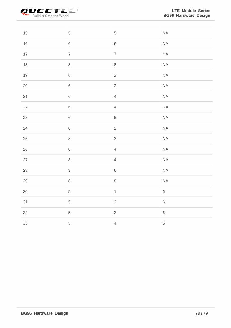
LTE Module Series BG96 Hardware Design
BG96_Hardware_Design 78 / 79
15 5 5 NA
16 6 6 NA
17 7 7 NA
18 8 8 NA
19 6 2 NA
20 6 3 NA
21 6 4 NA
22 6 4 NA
23 6 6 NA
24 8 2 NA
25 8 3 NA
26 8 4 NA
27 8 4 NA
28 8 6 NA
29 8 8 NA
30 5 1 6
31 5 2 6
32 5 3 6
33 5 4 6
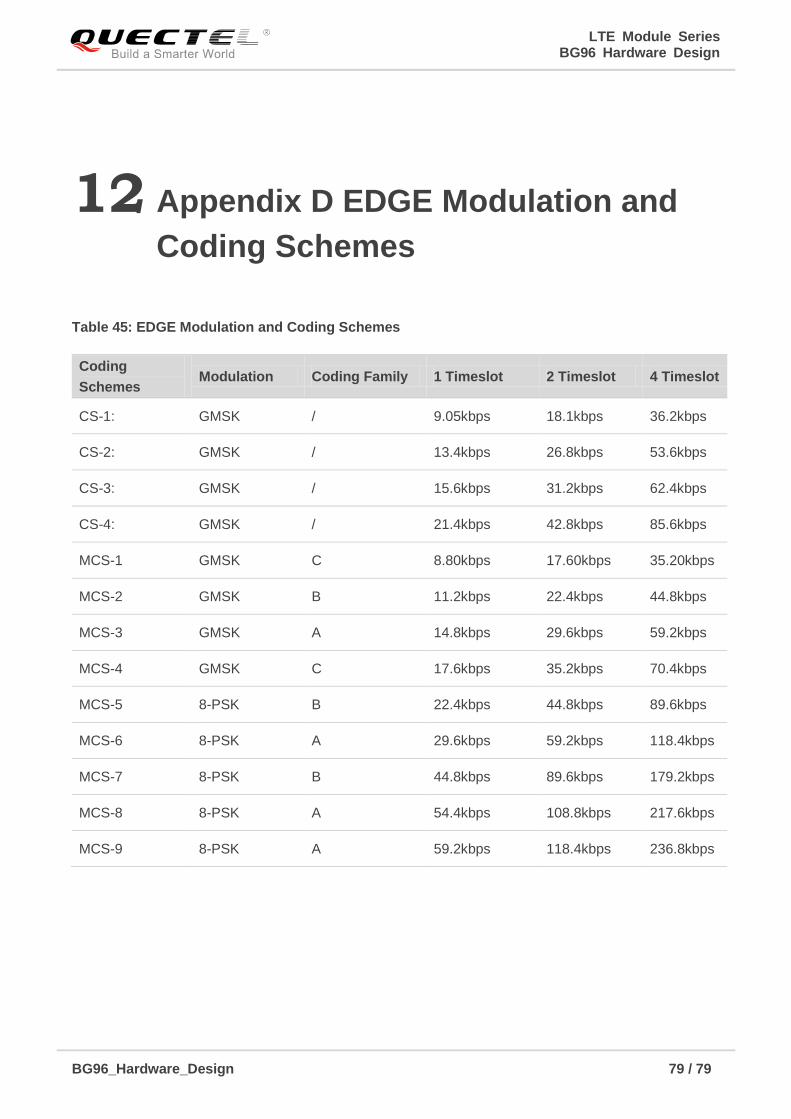
LTE Module Series BG96 Hardware Design
BG96_Hardware_Design 79 / 79
12 Appendix D EDGE Modulation and
Coding Schemes
Table 45: EDGE Modulation and Coding Schemes
Coding
Schemes Modulation Coding Family 1 Timeslot 2 Timeslot 4 Timeslot
CS-1: GMSK / 9.05kbps 18.1kbps 36.2kbps
CS-2: GMSK / 13.4kbps 26.8kbps 53.6kbps
CS-3: GMSK / 15.6kbps 31.2kbps 62.4kbps
CS-4: GMSK / 21.4kbps 42.8kbps 85.6kbps
MCS-1 GMSK C 8.80kbps 17.60kbps 35.20kbps
MCS-2 GMSK B 11.2kbps 22.4kbps 44.8kbps
MCS-3 GMSK A 14.8kbps 29.6kbps 59.2kbps
MCS-4 GMSK C 17.6kbps 35.2kbps 70.4kbps
MCS-5 8-PSK B 22.4kbps 44.8kbps 89.6kbps
MCS-6 8-PSK A 29.6kbps 59.2kbps 118.4kbps
MCS-7 8-PSK B 44.8kbps 89.6kbps 179.2kbps
MCS-8 8-PSK A 54.4kbps 108.8kbps 217.6kbps
MCS-9 8-PSK A 59.2kbps 118.4kbps 236.8kbps