Embed Size (px)
Citation preview
Beyond 40 GHz:Chips to be tested, Instruments to measure them
Mark RodwellUniversity of California, Santa Barbara
[email protected] 805-893-3244, 805-893-3262 fax
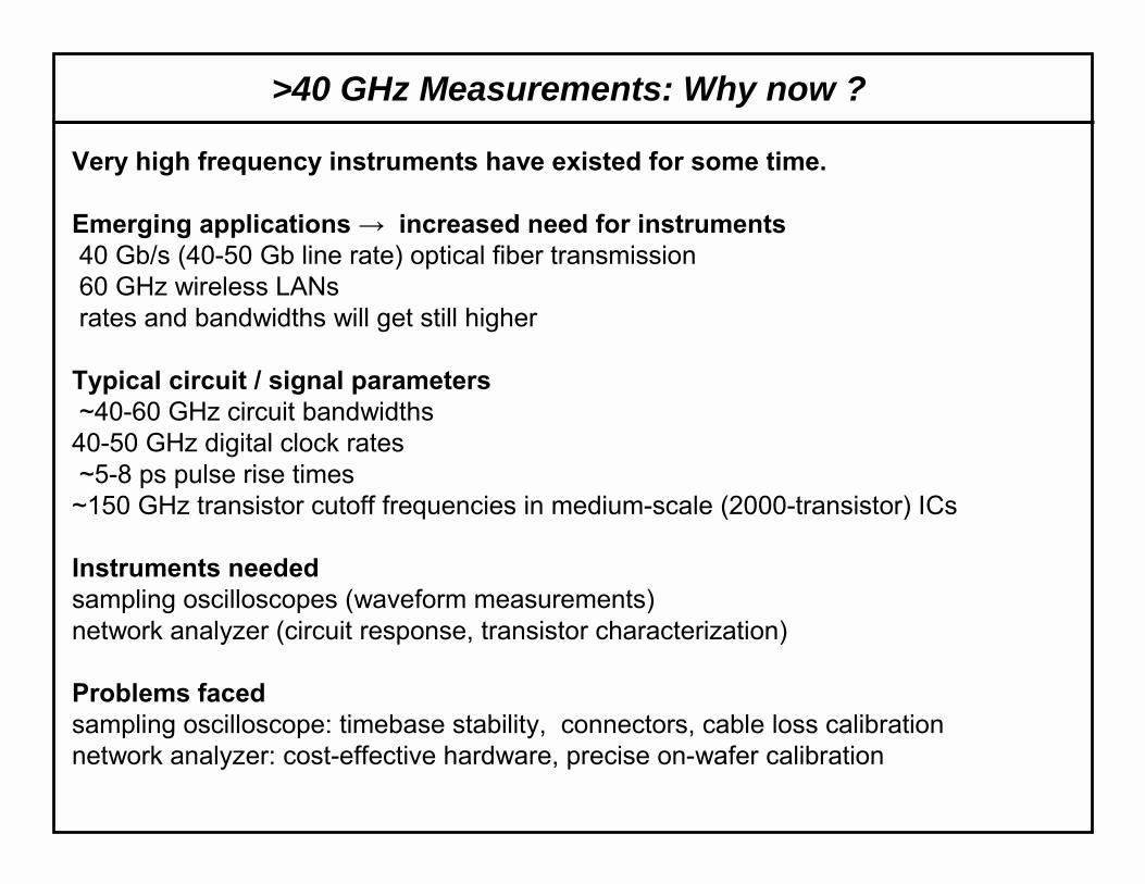
>40 GHz Measurements: Why now ?
Very high frequency instruments have existed for some time.
Emerging applications → increased need for instruments40 Gb/s (40-50 Gb line rate) optical fiber transmission60 GHz wireless LANsrates and bandwidths will get still higher
Typical circuit / signal parameters~40-60 GHz circuit bandwidths
40-50 GHz digital clock rates~5-8 ps pulse rise times
~150 GHz transistor cutoff frequencies in medium-scale (2000-transistor) ICs
Instruments neededsampling oscilloscopes (waveform measurements)network analyzer (circuit response, transistor characterization)
Problems facedsampling oscilloscope: timebase stability, connectors, cable loss calibrationnetwork analyzer: cost-effective hardware, precise on-wafer calibration
types of measurements and problems

High-Frequency Measurements: Network Analysis
Circuit frequency response
No extrapolation
Acceptable errors (roughly)~ 0.25 dB in S2130 dB directivity
0
2
4
6
8
10
140 150 160 170 180 190 200
S 21 (d
B)
Frequency (GHz)
Device characterization
S-parameters convertedto Yij and Zij
Frequency variation allowsdevice parameter extraction.
Calibration must be very precise
S22
S12x10S21/10
S11
Ccb,x = 7.1 fF
Rbc = 25 kΩΩΩΩ
Ccb,i = 2.3 fFRbb = 23 ΩΩΩΩ
Cje
Cdiff rbeVbe
rce==250k ΩΩΩΩ
Cpoly= 1.5 fFRex=4.23 ΩΩΩΩ Cout=1 fF
gmVbeexp[-jωωωω(0.23ps)]
rbe=112.5 ΩΩΩΩ, Cje = 47.4 fFCdiff = gm ττττf , ττττf = 0.8866 ps
gm = Ic/VT= 0.239
Base
Emitter
Collector
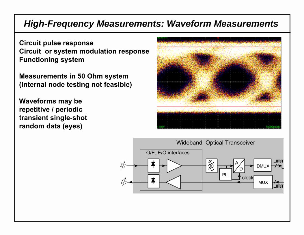
High-Frequency Measurements: Waveform Measurements
Circuit pulse responseCircuit or system modulation responseFunctioning system
Measurements in 50 Ohm system(Internal node testing not feasible)
Waveforms may berepetitive / periodictransient single-shotrandom data (eyes)
Wideband Optical Transceiver
clockPLL
AD DMUX
O/E, E/O interfaces
MUX

Network Analysis: system-level
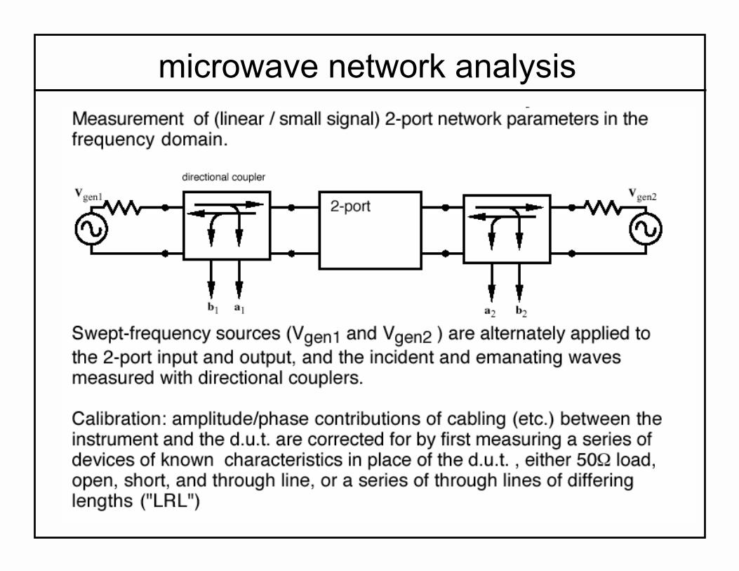
microwave network analysis
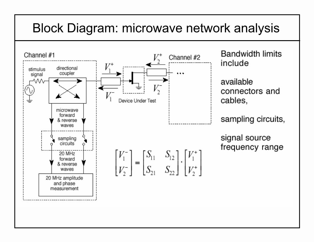
Block Diagram: microwave network analysis

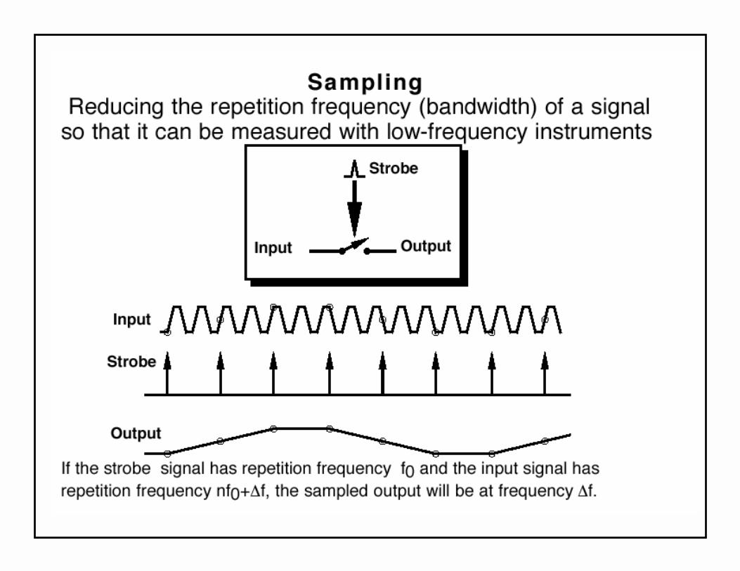
sampling oscilloscopes
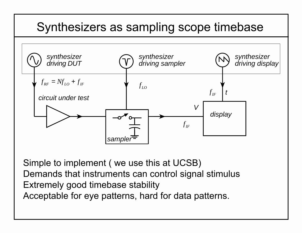
Synthesizers as sampling scope timebase
Simple to implement ( we use this at UCSB)Demands that instruments can control signal stimulusExtremely good timebase stabilityAcceptable for eye patterns, hard for data patterns.
synthesizerdriving display
synthesizerdriving sampler
circuit under test
displayV
t
sampler
synthesizerdriving DUT
LOfIFLORF fNff +=
IFf
IFf

Common triggered-timebase sampling scope
recognizetriggerevent
delay(variable)
delay rampgenerator
displayV
t
sampler
Good: trigger on aperiodic repetitive signalBad: no band limiting in triggering → trigger jitter
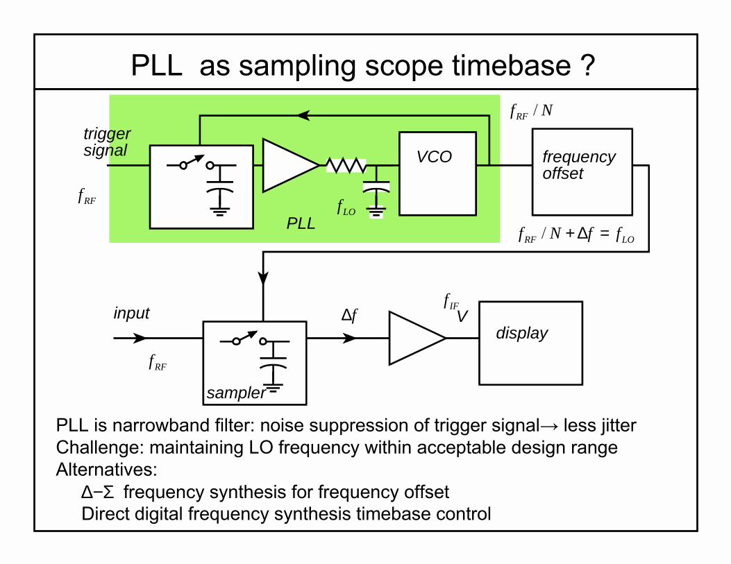
PLL
displayV
sampler
VCOtriggersignal frequency
offset
input
PLL as sampling scope timebase ?
PLL is narrowband filter: noise suppression of trigger signal→ less jitterChallenge: maintaining LO frequency within acceptable design rangeAlternatives:
∆−Σ frequency synthesis for frequency offsetDirect digital frequency synthesis timebase control
LOf
NfRF /
IFf
LORF ffNf =∆+/
f∆
RFf
RFf
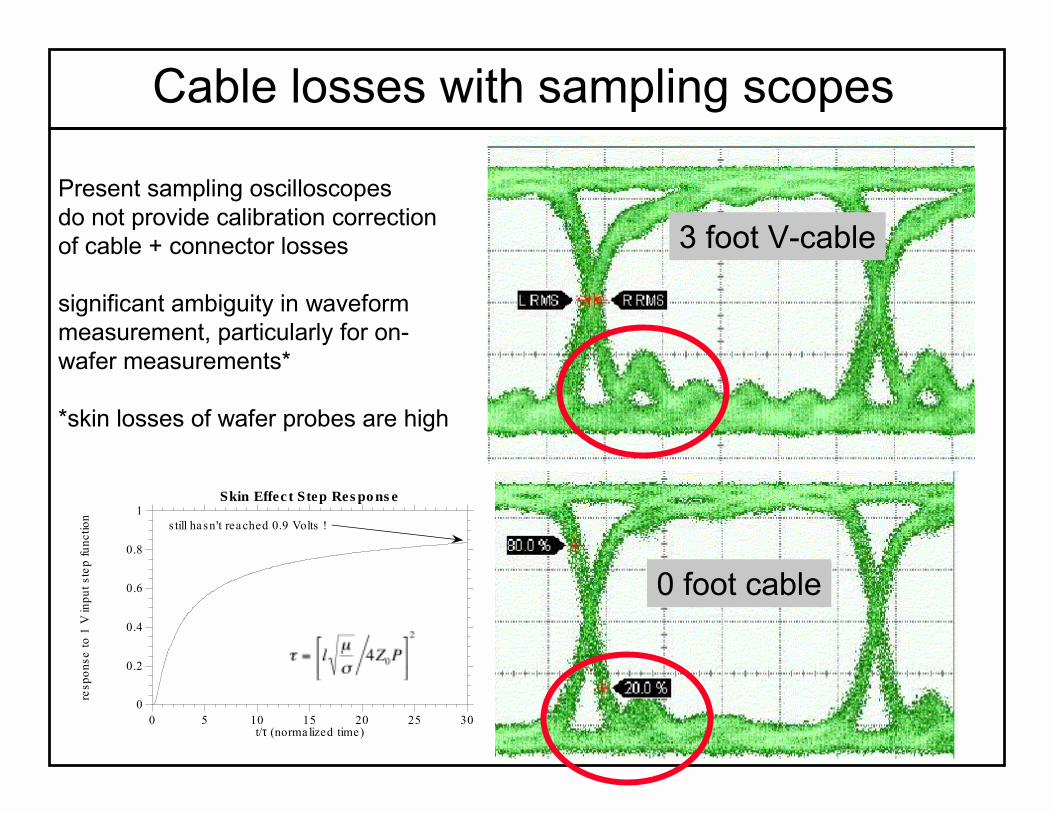
Cable losses with sampling scopes
Present sampling oscilloscopesdo not provide calibration correction of cable + connector losses
significant ambiguity in waveform measurement, particularly for on-wafer measurements*
*skin losses of wafer probes are high
0
0.2
0.4
0.6
0.8
1
0 5 10 15 20 25 30
Skin Effec t Step Res po ns e
resp
onse
to 1
V in
put s
tep
func
tion
t/τ (norma lized time)
s till ha sn't reached 0.9 Volts !
3 foot V-cable
0 foot cable
Calibration in sampling oscilloscopes ?
Pulse response distortion due to cable loss is becoming major measurement limit.
Network analysis removes such artifacts by calibration
Can NWA calibration be extended to sampling oscilloscopes ?

sampling bridgesand harmonic mixers

Equivalence of sampling and harmonic mixing
Frequency
spectrum of sampling pulse train
Frequency
spectrum of input signal
Frequency
spectrum of IF (sampled) signal
Sampling circuits are one type of high-order harmonic mixer.Sampling circuits used in oscilloscopes and network analyzers
LOfLOf2 LONf
IFLORF fNff +=
IFf

Harmonic-mixing order in network analysis
range dynamicbest hardware expensive
mixing lfundamenta with analysisNetwork
bridge samplingor pair diode bemay mixer harmonic figure noisebetter
tuningLO more LO,higher :hardware expensive moderately orders harmonic low with analysisNetwork
figure noisehigh todue range dynamic degraded tuningLO low frequency, lowat LO :hardware einexpensiv
:orders harmonichigh low with circuits Sampling
n)descriptiodomain (time on) / timeoff (time n)descriptiodomain (frequency conversion oforder harmonic
Circuit Sampling of figure Noise
≥≥
FF
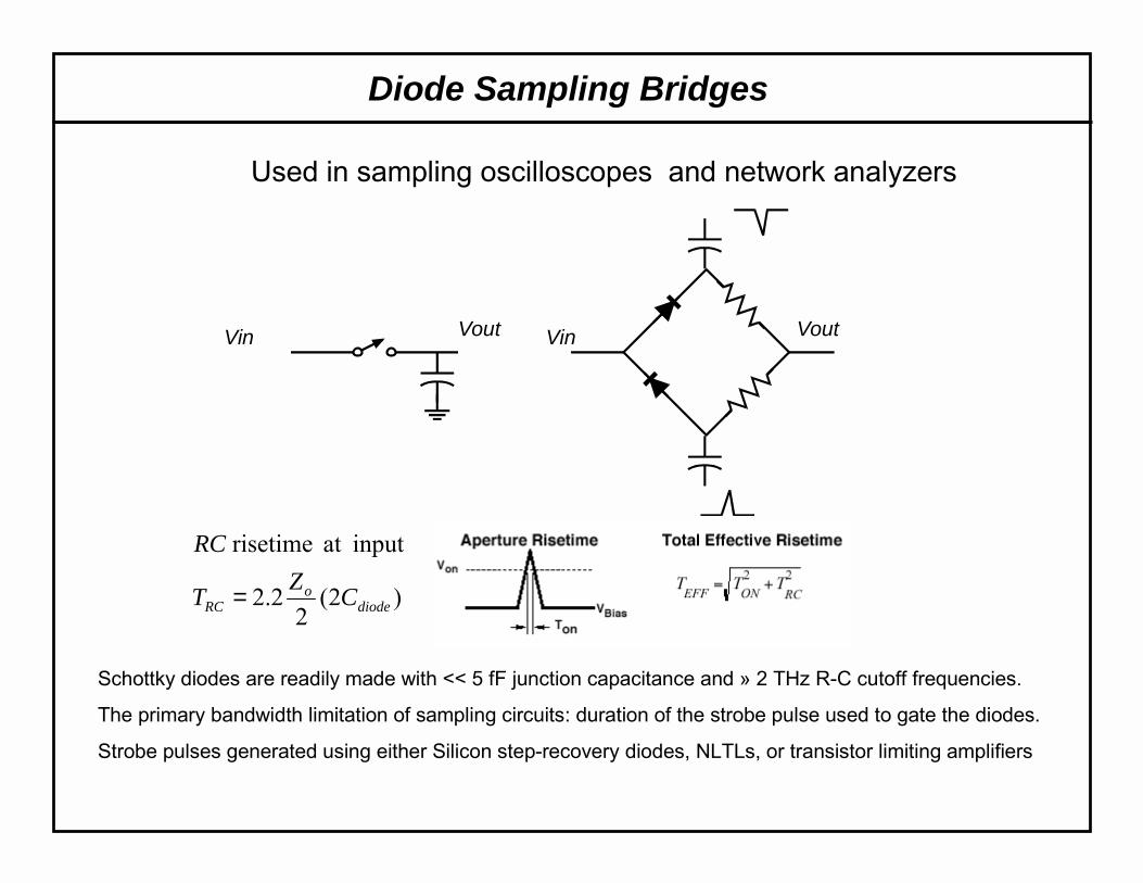
Diode Sampling Bridges
Used in sampling oscilloscopes and network analyzers
Vin VoutVin Vout
)2(2
2.2
inputat risetime
diodeo
RC CZT
RC
=
Schottky diodes are readily made with << 5 fF junction capacitance and » 2 THz R-C cutoff frequencies.
The primary bandwidth limitation of sampling circuits: duration of the strobe pulse used to gate the diodes.
Strobe pulses generated using either Silicon step-recovery diodes, NLTLs, or transistor limiting amplifiers


Risetime / pulse width limits to SRDs
ps 30-20 are devices available-commonlyBest ePerformanc Typical
widthdepletion ofps/micron 10 as thisestimates (1969) Moll regiondepletion in arises collapsecarrier finalin which Time
TimeDiffision Carrier
eCapacitancDepletion
SRDoCZ=τ

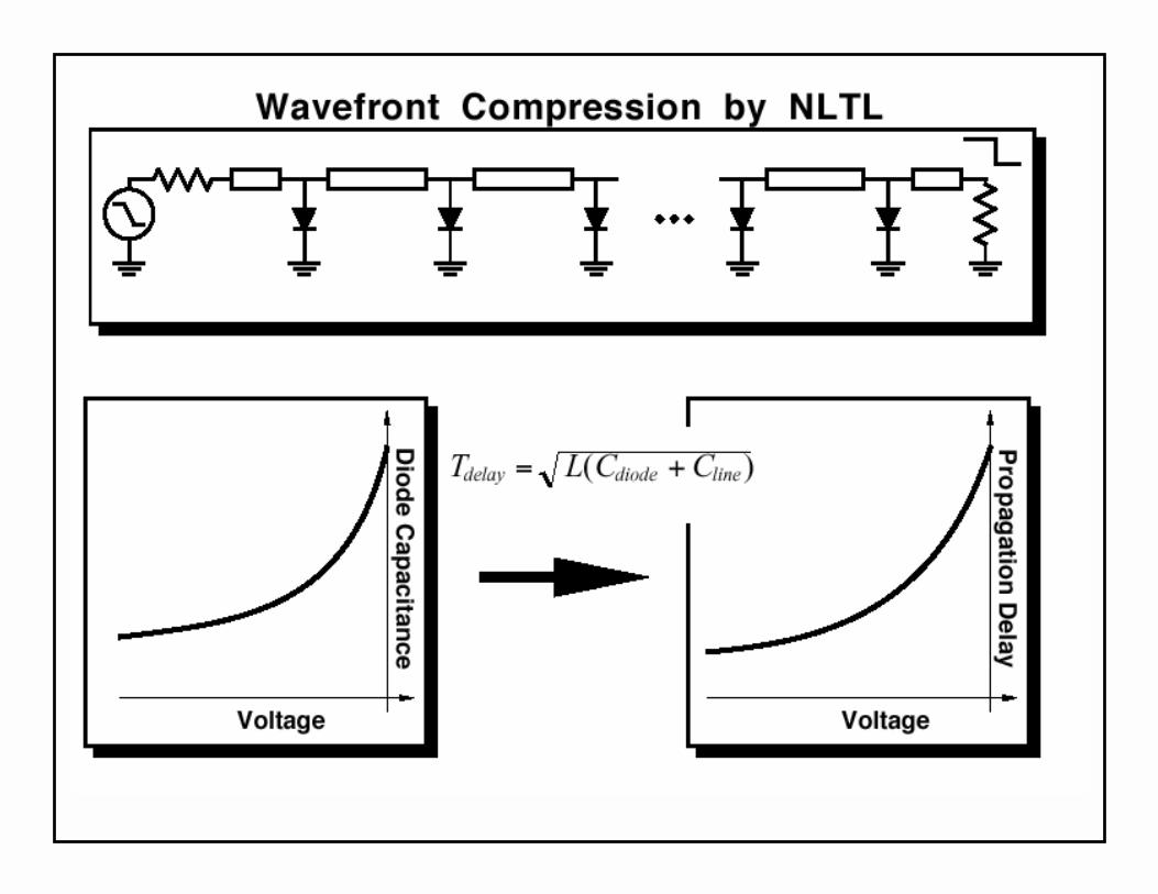
NLTL technology
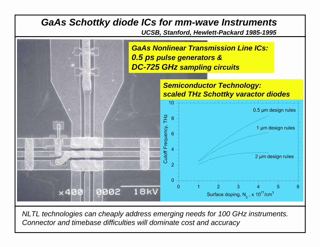
GaAs Schottky diode ICs for mm-wave Instruments
GaAs Nonlinear Transmission Line ICs:0.5 ps pulse generators & DC-725 GHz sampling circuits
0
2
4
6
8
10
0 1 2 3 4 5 6
Cut
off F
requ
ency
, TH
z
Surface doping, N0 , x 1017/cm3
0.5 µm design rules
1 µm design rules
2 µm design rules
Semiconductor Technology:scaled THz Schottky varactor diodes
UCSB, Stanford, Hewlett-Packard 1985-1995
NLTL technologies can cheaply address emerging needs for 100 GHz instruments. Connector and timebase difficulties will dominate cost and accuracy
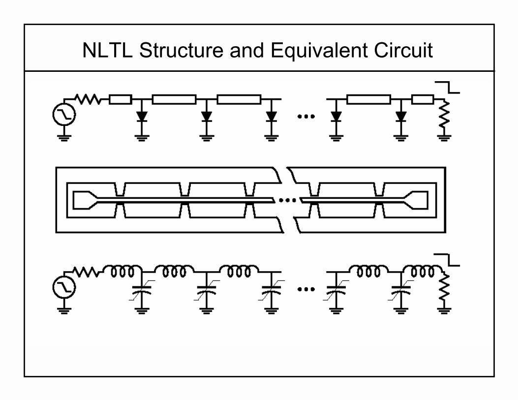
NLTL Structure and Equivalent Circuit
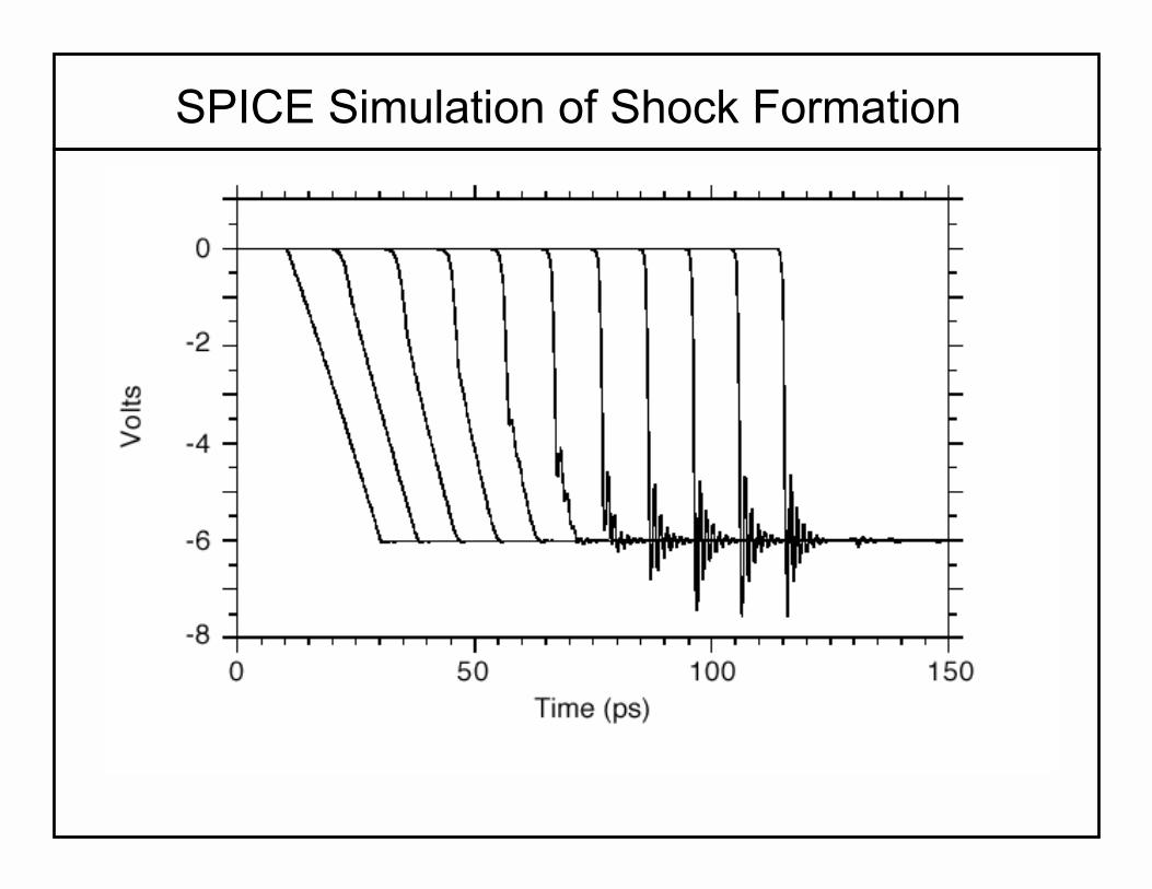
SPICE Simulation of Shock Formation
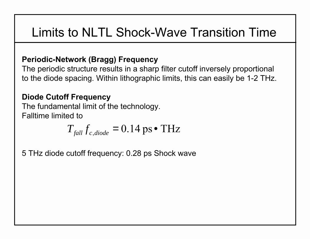
Limits to NLTL Shock-Wave Transition Time
Periodic-Network (Bragg) FrequencyThe periodic structure results in a sharp filter cutoff inversely proportionalto the diode spacing. Within lithographic limits, this can easily be 1-2 THz.
Diode Cutoff FrequencyThe fundamental limit of the technology.Falltime limited to
5 THz diode cutoff frequency: 0.28 ps Shock wave
THzps 14.0, •=diodecfall fT

τ2
τ
τ2τ
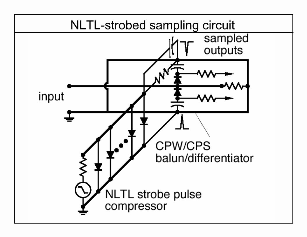
NLTL-strobed sampling circuit
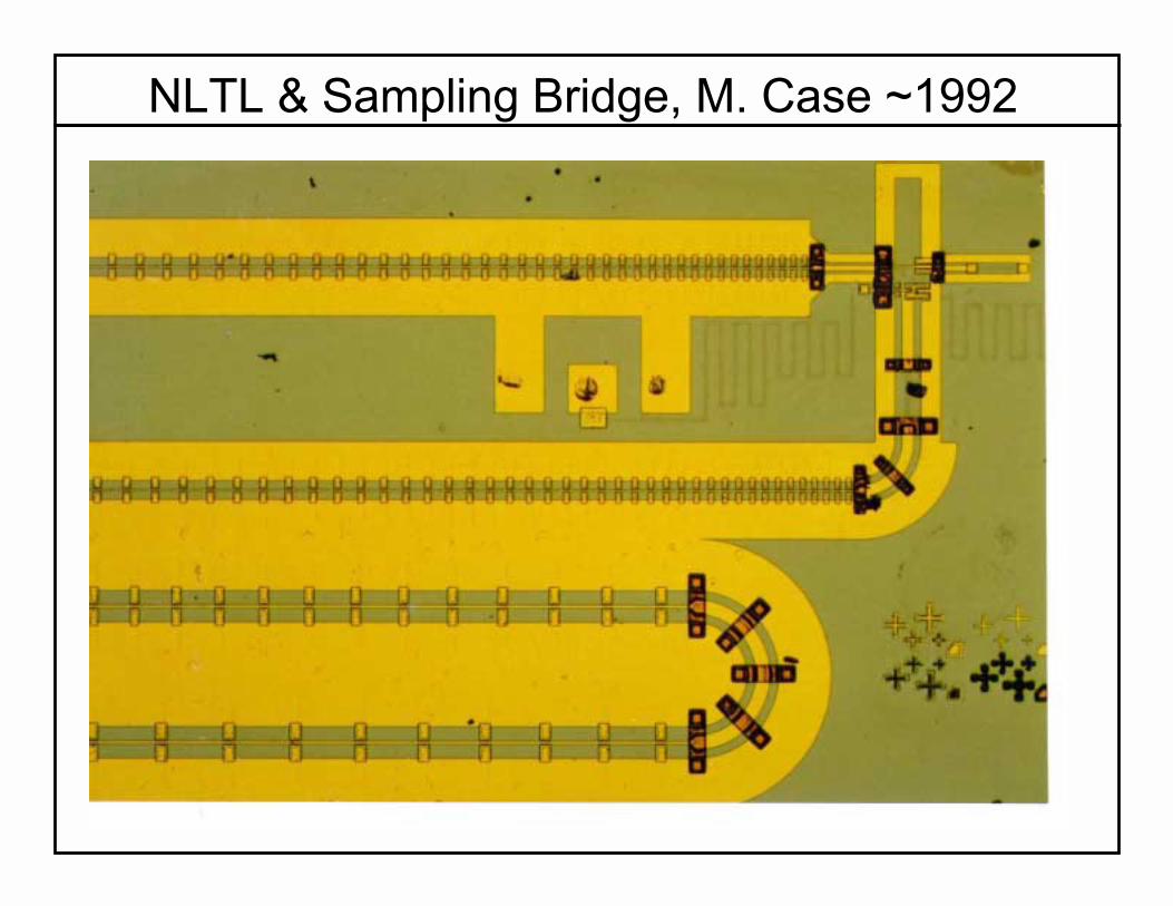
NLTL & Sampling Bridge, M. Case ~1992
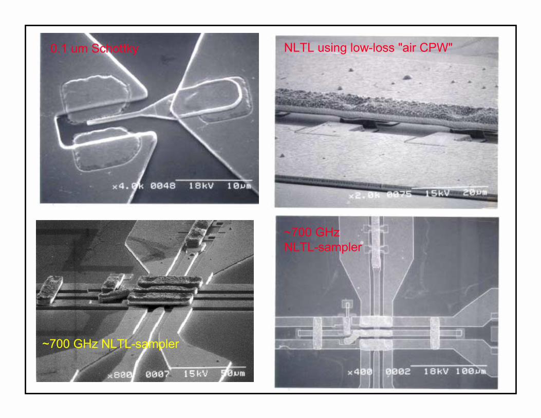
0.1 um Schottky
~700 GHz NLTL-sampler
NLTL using low-loss "air CPW"
~700 GHz NLTL-sampler
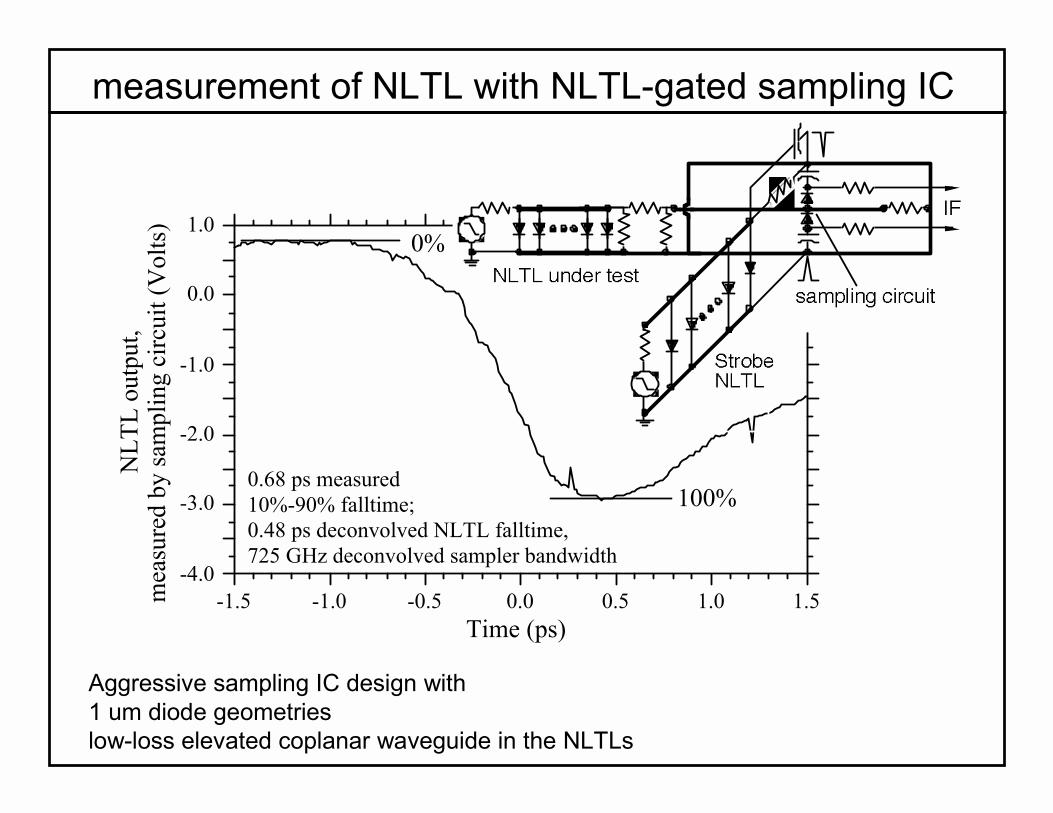
measurement of NLTL with NLTL-gated sampling IC
-4.0
-3.0
-2.0
-1.0
0.0
1.0
NLT
L ou
tput
, m
easu
red
by sa
mpl
ing
circ
uit (
Vol
ts)
-1.5 -1.0 -0.5 0.0 0.5 1.0 1.5
0%
100%
Time (ps)
0.68 ps measured10%-90% falltime;0.48 ps deconvolved NLTL falltime,725 GHz deconvolved sampler bandwidth
Aggressive sampling IC design with 1 um diode geometrieslow-loss elevated coplanar waveguide in the NLTLs
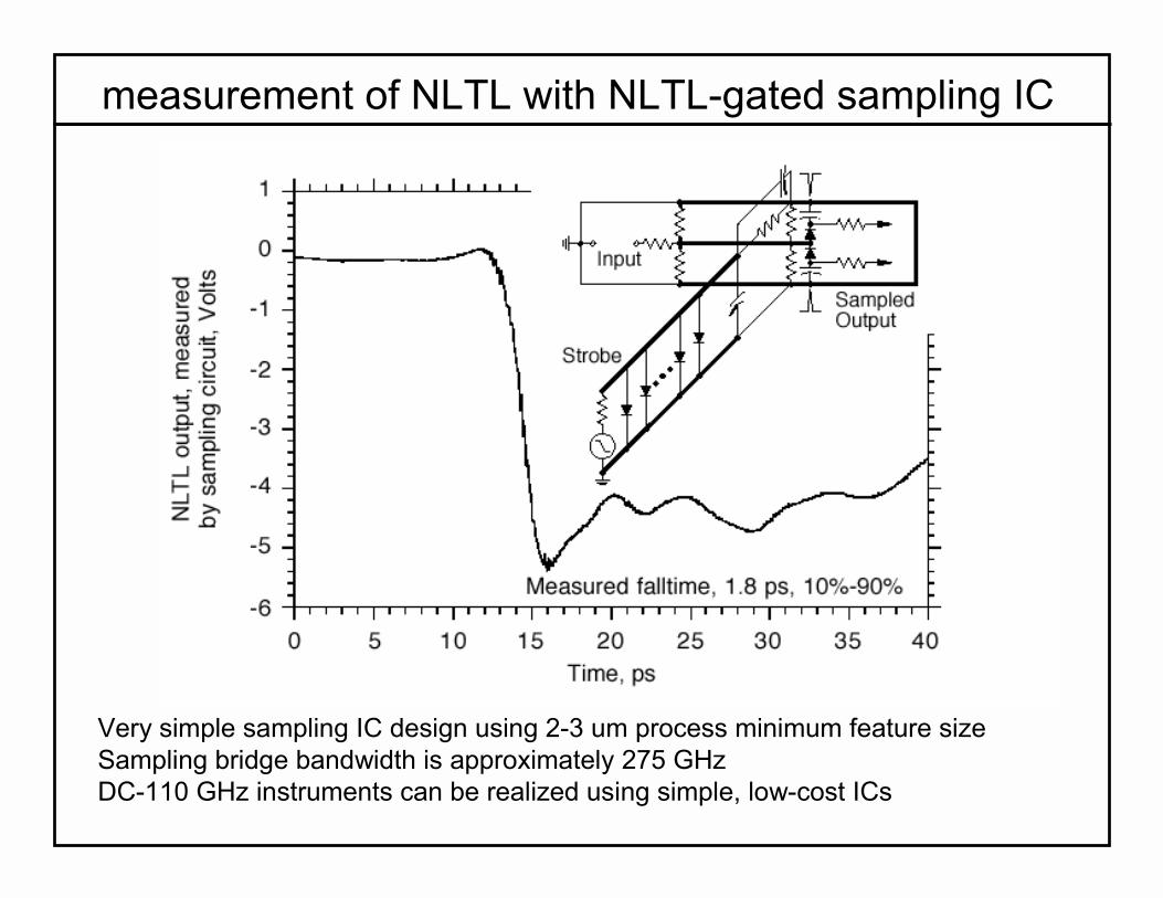
measurement of NLTL with NLTL-gated sampling IC
Very simple sampling IC design using 2-3 um process minimum feature sizeSampling bridge bandwidth is approximately 275 GHzDC-110 GHz instruments can be realized using simple, low-cost ICs
Prospective for use of NLTLs in InstrumentsNLTLs have been used commercially since early 1990's HP/Agilent 50 GHz sampling oscilloscopesMicrowave transition analyzer45 MHz -- 50 GHz 8510 network analyzer ?Recent emergence of higher-frequency markets now driving instruments
Less Expensive 45 MHz -110 GHz network analysisPresent systems frequency-combine waveguide-banded systems.
These are accurate but expensive.Reduced-cost instrument could use NLTL-driven sampler for down conversion
NLTL-based sampler can easily down convert DC-200 GHzUse DC-10 GHz synthesized source for LOMixing harmonic order <11 in DC-110 GHz bandwidth: good dynamic rangemain design challenge: LO drive interface to NLTL input
Wider-bandwidth sampling oscilloscopes Present instruments are DC-65 GHz, some are NLTL-based.It is easy to build NLTL-gated samplers far faster than this. Practical limits to DC-110 GHz oscilloscope development are:
timebase stability (eliminating trigger jitter)connector bandwidth limit (110 GHz connectors are fragile)correction of connection (cable, wafer probe) frequency response by calibration.
High FrequencyNetwork Analysis
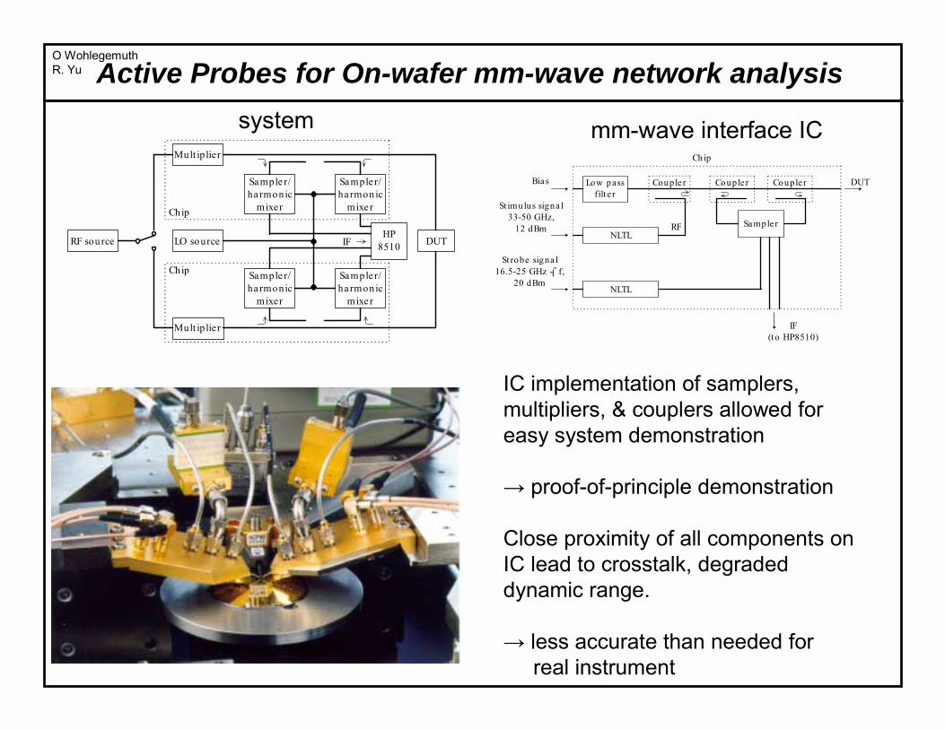
Active Probes for On-wafer mm-wave network analysis
Sample r/ha rmonic
mixer
Sample r/ha rmonic
mixer
RF source
Sample r/ha rmonic
mixer
Mult iplier
LO sourceHP
8510
Sample r/ha rmonic
mixer
Mult iplier
DUT
Chip
Chip
IF
Couple rLow passfilt e r
St imulus signa l33-50 GHz,
12 dBm
Couple r Couple r
St robe signa l16.5-25 GHz -⌠f,
20 dBm
DUTBias
NLTL
Chip
IF(t o HP8510)
RF Sampler
NLTL
mm-wave interface ICsystem
IC implementation of samplers, multipliers, & couplers allowed for easy system demonstration
→ proof-of-principle demonstration
Close proximity of all components on IC lead to crosstalk, degraded dynamic range.
→ less accurate than needed for real instrument
O WohlegemuthR. Yu

Fraunhofer / UCSB 70-220 GHz Network AnalyzerO WohlegemuthR. Yu
O. Wohlgemuth et al IEEE Transactions on Microwave Theory and Techniques, Vol. 47, No. 12, December.1999
Chip Flexible (GGB)
probe-tip Buffer
amplifier

Fraunhofer / UCSB 70-220 GHz Network Analyzer
80 100 120 140 160 180 200 220-40
-30
-20
-10
0
Mag
nitu
de S
11 [d
B]
Frequency [GHz]
Measurement of S11 of a 900 µm line.
220 GHz
fstart = 70.0 GHz fstop = 230 GHz
Measurement of S21 of a 900 µm line.
O. Wohlgemuth et al IEEE Transactions on Microwave Theory and Techniques, Vol. 47, No. 12, December.1999
O WohlegemuthR. Yu
80 100 120 140 160 180 200 220-5
0
5
10
15
20
25
Dire
ctiv
ity [d
B]
Frequency [GHz]
Measured raw directivity of the ac-tive probe
80 100 120 140 160 180 200 220-60
-55
-50
-45
-40
-35
-30
-25
-20
Max
imum
pow
er [d
Bm]
Frequency [GHz]
Measured maximum power at the IF-ports.
Precision on-wafer > 40 GHznetwork analysis
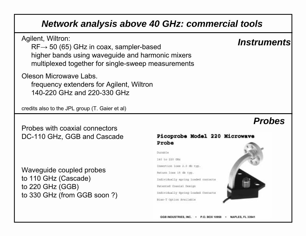
Network analysis above 40 GHz: commercial toolsAgilent, Wiltron:
RF→ 50 (65) GHz in coax, sampler-basedhigher bands using waveguide and harmonic mixersmultiplexed together for single-sweep measurements
Oleson Microwave Labs. frequency extenders for Agilent, Wiltron140-220 GHz and 220-330 GHz
credits also to the JPL group (T. Gaier et al)
Instruments
ProbesProbes with coaxial connectorsDC-110 GHz, GGB and Cascade
Waveguide coupled probes to 110 GHz (Cascade)to 220 GHz (GGB)to 330 GHz (from GGB soon ?)

On-wafer mm-wave Network Analysis at UCSBApplications:Measurements of transistor amplifiers to 220 GHzPrecise characterization of transistors (power gains, parameter extraction)
45 MHz-50 (40) GHz: Agilent 8510 NWA, coaxial cables and probes
75-110 GHz: Agilent 8510 NWA, waveguide, GGB waveguide-coupled probes
140-220 GHz: Oleson frequency extenders, waveguide, GGB waveguide-coupled probes
Key features for good measurements
on-wafer LRL microstrip calibration standards with offset reference planes
waveguide instrument-probe connections: less loss, less phase drift.
higher band instruments use low-order mixers → better dynamic range
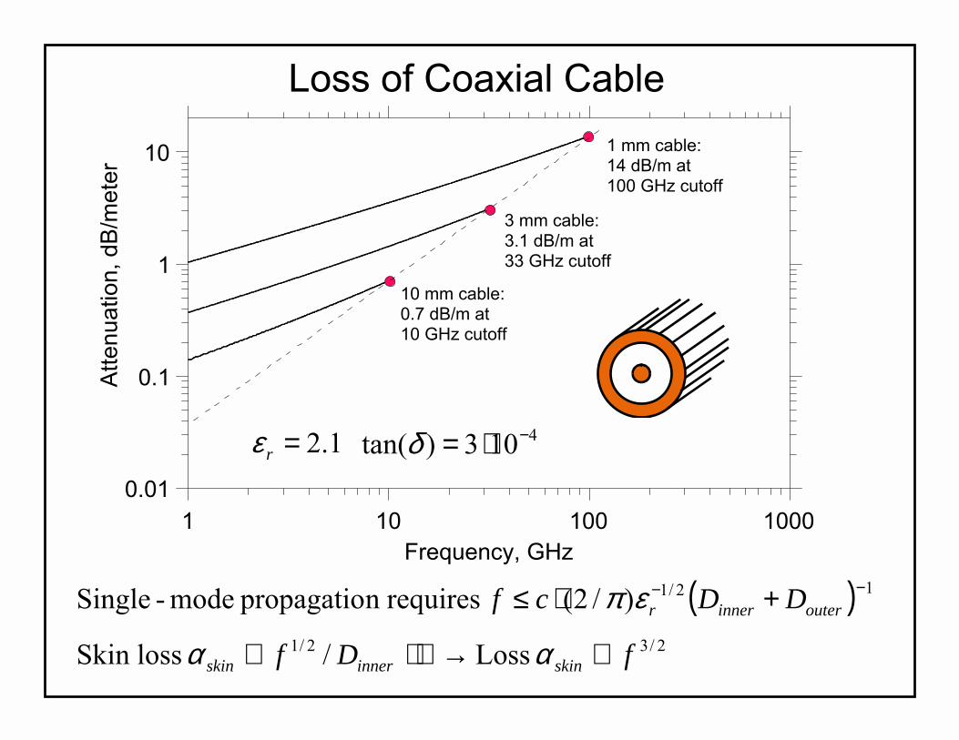
Loss of Coaxial Cable
0.01
0.1
1
10
1 10 100 1000
Atte
nuat
ion,
dB/
met
er
Frequency, GHz
10 mm cable:0.7 dB/m at10 GHz cutoff
3 mm cable:3.1 dB/m at33 GHz cutoff
1 mm cable:14 dB/m at 100 GHz cutoff
1.2=rε 4103)tan( −⋅=δ
( ) 12/1)/2( requiresn propagatio mode-Single −− +⋅≤ outerinnerr DDcf επ2/32/1 Loss / lossSkin fDf skininnerskin ∝→∝ αα
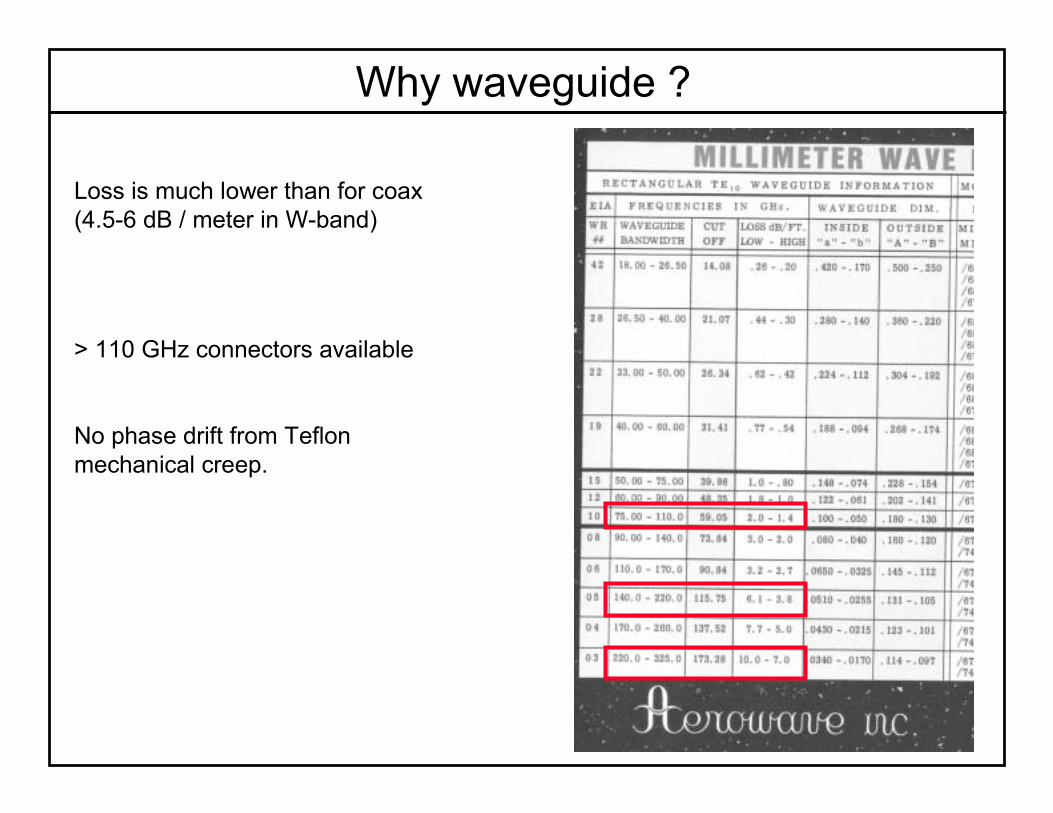
Why waveguide ?
Loss is much lower than for coax(4.5-6 dB / meter in W-band)
> 110 GHz connectors available
No phase drift from Teflon mechanical creep.
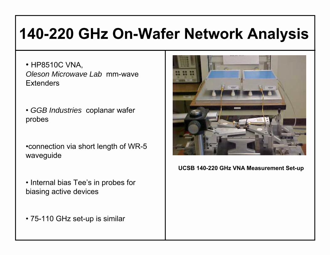
HP8510C VNA, Oleson Microwave Lab mm-wave Extenders
GGB Industries coplanar wafer probes
connection via short length of WR-5 waveguide
Internal bias Tees in probes for biasing active devices
75-110 GHz set-up is similar
140-220 GHz On-Wafer Network Analysis
UCSB 140-220 GHz VNA Measurement Set-up
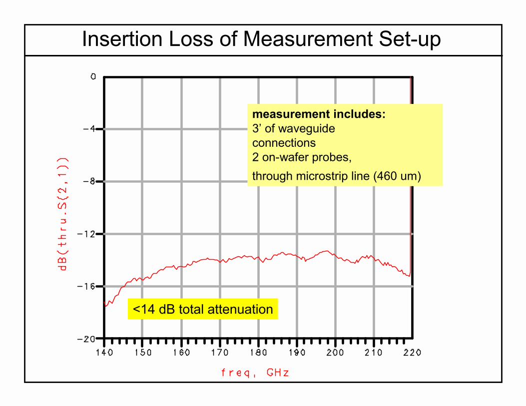
Insertion Loss of Measurement Set-up
<14 dB total attenuation
measurement includes:3 of waveguide connections2 on-wafer probes, through microstrip line (460 um)
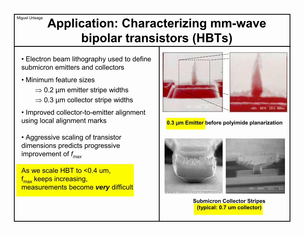
Application: Characterizing mm-wave bipolar transistors (HBTs)
Electron beam lithography used to define submicron emitters and collectors
Minimum feature sizes⇒ 0.2 µm emitter stripe widths ⇒ 0.3 µm collector stripe widths
Improved collector-to-emitter alignment using local alignment marks
Aggressive scaling of transistor dimensions predicts progressive improvement of fmax
As we scale HBT to <0.4 um, fmax keeps increasing,measurements become very difficult
0.3 µµµµm Emitter before polyimide planarization
Submicron Collector Stripes(typical: 0.7 um collector)
Miguel Urteaga
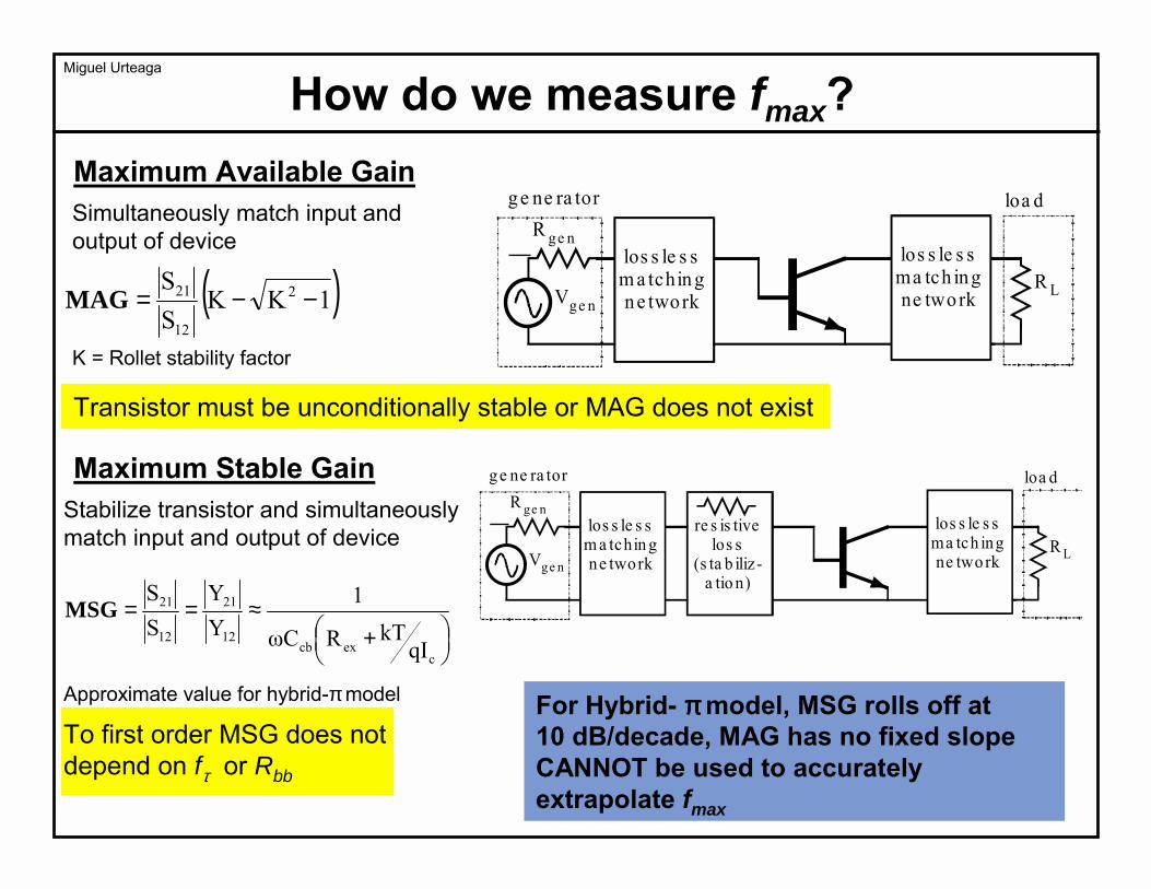
Stabilize transistor and simultaneously match input and output of device
Approximate value for hybrid-πmodel
To first order MSG does not depend on fτ or Rbb
Simultaneously match input and output of device
K = Rollet stability factor
How do we measure fmax?
( )1KKSS 2
12
21 −−=MAG
+
≈==
cexcb
12
21
12
21
qIkTRωC
1YY
SS
MSG
For Hybrid- ππππmodel, MSG rolls off at 10 dB/decade, MAG has no fixed slopeCANNOT be used to accurately extrapolate fmax
Maximum Available Gain
Transistor must be unconditionally stable or MAG does not exist
Maximum Stable Gain
ge ne ra tor
los s le s sm a tchin gne twork
R ge n
Vge n
los s le s sma tch ingne twork
R L
loa d
ge ne ra tor
los s le s sm a tchin gne twork
R ge n
Vge n
los s le s sma tch ingne twork
R L
loa d
re s is tivelos s
(s ta b iliz -a tio n)
Miguel Urteaga
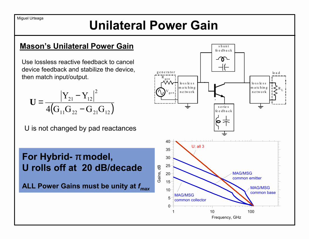
Use lossless reactive feedback to cancel device feedback and stabilize the device, then match input/output.
( )12212211
21221
GGGG4YY−
−=U
Unilateral Power GainMasons Unilateral Power Gain
0
5
10
15
20
25
30
35
40
1 10 100
Gai
ns, d
B
Frequency, GHz
MAG/MSGcommon base
U: all 3
MAG/MSGcommon collector
MAG/MSGcommon emitter
For Hybrid- ππππmodel, U rolls off at 20 dB/decade
ALL Power Gains must be unity at fmax
U is not changed by pad reactances
g e n e ra to r
lo s s le s sm a tc h in gn e tw o rk
R g e n
Vg e n
lo s s le s sm a tc h in gn e tw o rk
R L
lo a d
s e rie sfe e d b a c k
s h u n tfe e d b a c k
Miguel Urteaga
On-wafer NWA:
calibration problems
0
5
10
15
20
25
30
35
1 10 100Fre que ncy, GHz
MSG
h21
Ma son'sGa in, U
Submicron HBTs have very low Ccb (< 3 fF) Characterization requires accurate measure of very small S12 Standard 12-term VNA calibrations do not correct S12 background error due to probe-to-probe coupling
SolutionEmbed transistors in sufficient length of transmission line to reduce coupling
Place calibration reference planes at transistor terminals
Line-Reflect-Line CalibrationStandards easily realized on-wafer
Does not require accurate characterization of reflect standards
Characteristics of Line Standards are well controlled in transferred-substrate microstrip wiring environment
Accurate Transistor Measurements Are Not Easy
Transistor in Embedded in LRL Test Structure
230 µm 230 µm
Corrupted 75-110 GHz measurements due toexcessive probe-to-probe coupling
Miguel Urteaga

Line-reflect-line on-wafer cal. standards
Lo Lo
Lo Lo
Lo Lo
Lo+Lo
Lo+560 µm+Lo
Lo+1275 µm+Lo20-60 GHz LINE
75-110 GHz LINE
THROUGH LINE
SHORT
OPEN (reflect)
DUT
75-110 GHz Calibration standards
20-60 GHz Calibration standards
Calibration verification
Device under test
V= 2.04 x 10⁸ m/s(εr = 2.7)
Note that calibration is to line Zo : line Zo is complex at lower frequencies, and must be determined
On-wafer transmission-line wiring environment: impact on LRL calibration
8.3=rε
13=rε
13=rε
m 75 µ=h
m 5 µ=h
m 500 µ=h
Thin-film microstrip
precise LRL calibration
microstrip
might be OK: watch for substrate modesproblem with substrate modesthin wafer ? absorber ?
CPW
140 150 160 170 180 190 200 210 220
freq, GHz
-0.15
-0.10
-0.05
0.00
0.05
0.10
0.15
0.20
0.25
0.30
freq (75.00GHz to 110.0GHz)
How good is the calibration ?
freq (140.0GHz to 220.0GHz)
S11 of throughAbout 40 dB
140-220 GHz calibration looks OK75-110 GHz calibration looks Great
S11 of openAbout 0.1 dB / 3o error
dBS21 of through line is off by less than 0.05 dB
S11 of openS11 of short S11 of through
75 80 85 90 95 100 105 110
freq, GHz
-70
-65
-60
-55
-50
-45
-40
Probe-Probe couplingis better than 45 dB
Miguel Urteaga
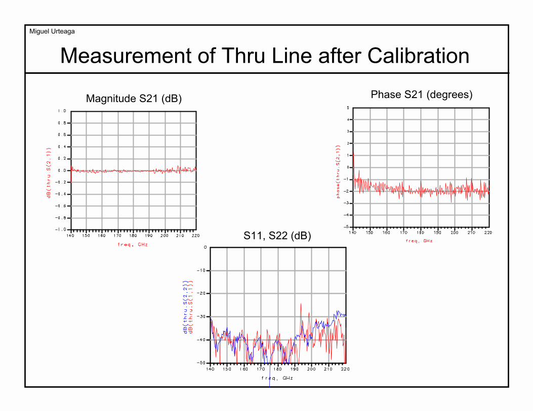
Measurement of Thru Line after Calibration
S11, S22 (dB)
Magnitude S21 (dB) Phase S21 (degrees)
Miguel Urteaga
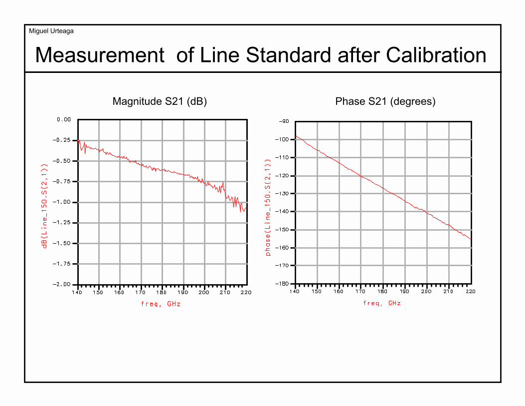
Measurement of Line Standard after Calibration
Magnitude S21 (dB) Phase S21 (degrees)
Miguel Urteaga
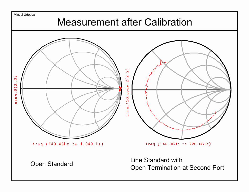
Measurement after Calibration
Open Standard Line Standard with Open Termination at Second Port
Miguel Urteaga
On-wafer NWA:
results with good LRL calibration
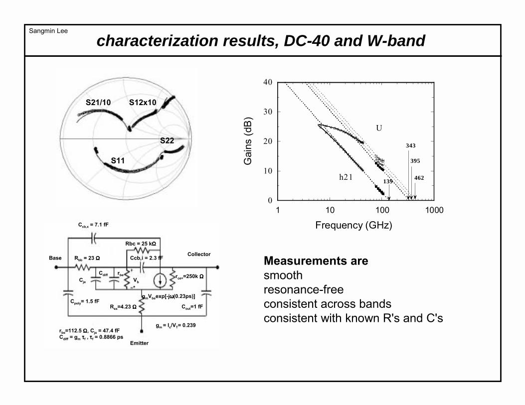
characterization results, DC-40 and W-band
Measurements are smoothresonance-freeconsistent across bandsconsistent with known R's and C's
0
10
20
30
40
1 10 100 1000
Gai
ns (d
B)
Frequency (GHz)
U
h21 462
395
343
139
S22
S12x10S21/10
S11
Ccb,x = 7.1 fF
Rbc = 25 kΩΩΩΩ
Ccb,i = 2.3 fFRbb = 23 ΩΩΩΩ
Cje
Cdiff rbeVbe
rce==250k ΩΩΩΩ
Cpoly= 1.5 fFRex=4.23 ΩΩΩΩ Cout=1 fF
gmVbeexp[-jωωωω(0.23ps)]
rbe=112.5 ΩΩΩΩ, Cje = 47.4 fFCdiff = gm ττττf , ττττf = 0.8866 ps
gm = Ic/VT= 0.239
Base
Emitter
Collector
Sangmin Lee
S11
S22
-6 -4 -2 0 2 4 6
freq (6.000GHz to 45.00GHz)
S12*20
S21
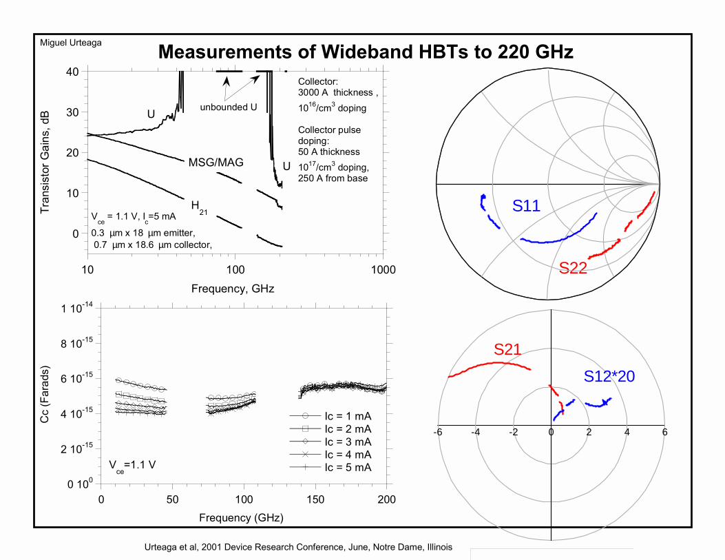
Measurements of Wideband HBTs to 220 GHz
Urteaga et al, 2001 Device Research Conference, June, Notre Dame, Illinois
0
10
20
30
40
10 100 1000
Tran
sist
or G
ains
, dB
Frequency, GHz
U
UMSG/MAG
H21
unbounded U
Collector: 3000 A thickness , 1016/cm3 doping
Collector pulse doping: 50 A thickness 1017/cm3 doping, 250 A from base
Vce
= 1.1 V, Ic=5 mA
0.3 µm x 18 µm emitter, 0.7 µm x 18.6 µm collector,
0 100
2 10-15
4 10-15
6 10-15
8 10-15
1 10-14
0 50 100 150 200
Ic = 1 mAIc = 2 mAIc = 3 mAIc = 4 mAIc = 5 mA
Cc
(Far
ads)
Frequency (GHz)
Vce
=1.1 V
Miguel Urteaga
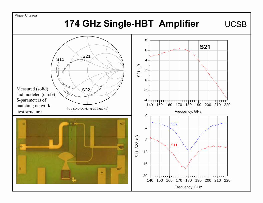
150 160 170 180 190 200 210140 220
-2
0
2
4
6
-4
8
Frequency, GHz
S2
1, d
B
150 160 170 180 190 200 210140 220
-16
-12
-8
-4
-20
0
Frequency, GHz
S1
1, S
22
, dB
S11
S22
S21
174 GHz Single-HBT Amplifier UCSB
freq (140.0GHz to 220.0GHz)
S11
S22
S21
Measured (solid) and modeled (circle) S-parameters of matching networktest structure
Miguel Urteaga
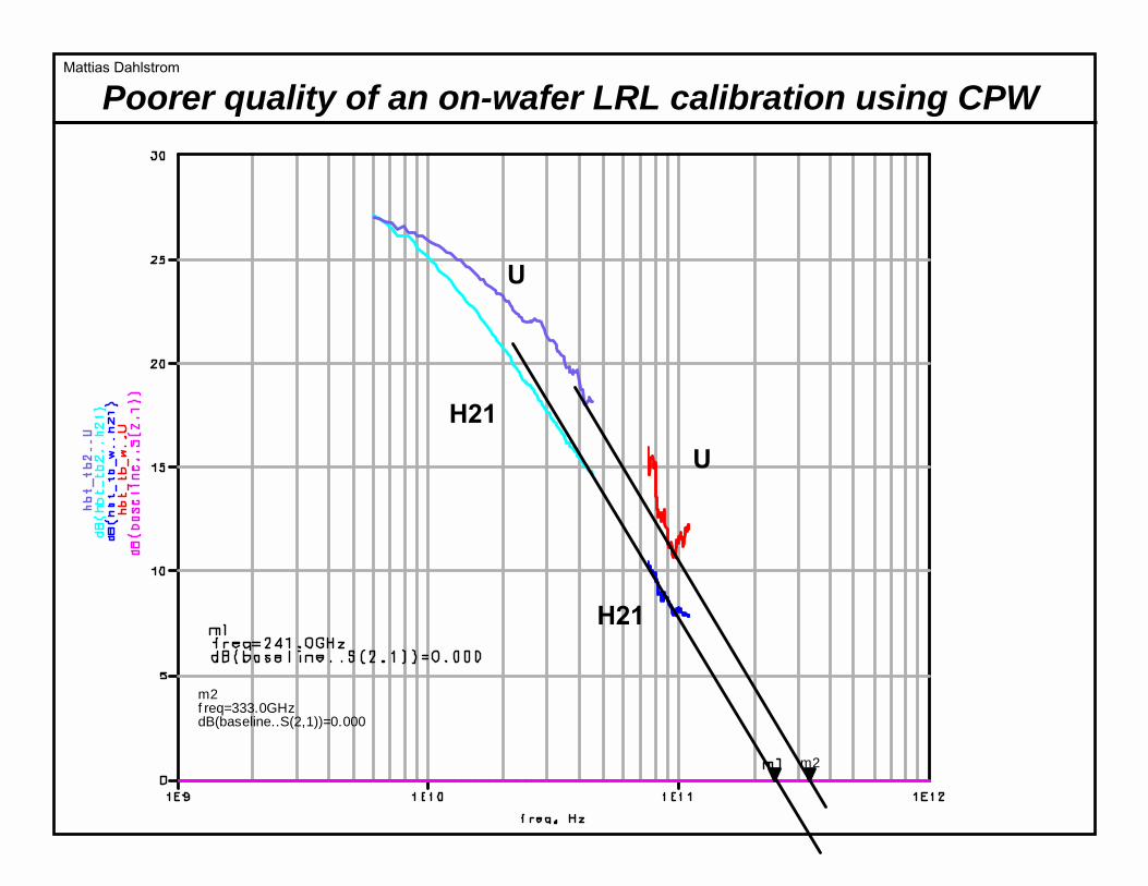
m2f req=333.0GHzdB(baseline..S(2,1))=0.000
m2
Poorer quality of an on-wafer LRL calibration using CPW
H21
H21
U
U
Mattias Dahlstrom
High Frequency Instruments
Needs:100 GHz sampling oscilloscopes for 40 Gb fiber transmission, Accurate and affordable 60 GHz (100 GHz ?) network analyzers
Easy to Address: sampling (harmonic down conversion) is easy and cheap over DC-200+ GHzother problems are relevant
Sampling Oscilloscopestimebase stability and flexibility in triggering: conflicting requirements !better time bases: 3-synthesizer, PLL, or DDFSchoose timebase appropriate for applicationcable losses are major source of errornetwork-analyzer-like calibration procedures should be developed
Network Analysiscombined accuracy, frequency coverage, and costgood solution (?): moderate-order harmonic conversion with sampler for 40-110 GHzbetter calibration methods needed for testing > 300 GHz ft and fmax transistors