Embed Size (px)
Citation preview

Beta rolloff & Avalanche breakdown
Presented byHEITHEM SOUISSI

Beta
Rolloff

�Beta= Current gain for a BJT
�Beta is commonly referred to as a constant,although it varies considerably depending onthe collector current.

�High current beta rolloff is caused by high-level injection.
�Low current beta rolloff results fromrecombination, and shallow emitter effect.
� The lateral PNP beta curve is different from that of anNPN for several reasons
� Due to its light doping,PNP exhibits lower emitterinjection efficiency that reduces its beta peak.
� The flow of carriers near the surface of the PNPincreases surface recombination, causing low-currentbeta rolloff.
� The lightly doped base of the PNP causes high levelinjections to begin at relatively low current levels,therefore high current beta rolloff.

Avalanche
Breakdown

� Deleterious effect that occurs in the presence of high electricfield.
� Causes high resistance elements to allow flow of highcurrent.
� Typically an irreversible effect permanently damaging theelement.

Avalanche/Zener Breakdown
� 'Zener diode' and 'avalanche diode' are terms often usedinterchangeably.
� Both refer to breakdown of a diode under reverse bias.
Avalanche/Zener Breakdown(con’t)
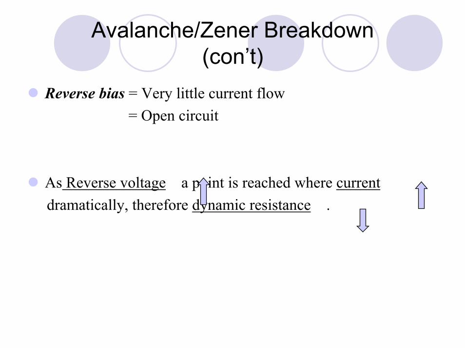
� Reverse bias = Very little current flow = Open circuit
� As Reverse voltage a point is reached where current dramatically, therefore dynamic resistance .

Avalanche Breakdown
Avalanche breakdown causes high flow of current underreverse bias condition!
The question is: How does this happen?

Avalanche Breakdown (con’t)
Reverse bias Thick depletion region causes high electric field and tremendous acceleration
Very few electrons make it through depletion region
These electrons collide with atoms in the depletion region and free more electrons ( Process called Multiplication).
Results in higher and higher current flow.
By analogy, the process is namedbecause a single carrier can spawnliterally thousands of additional carriersthrough collisions, just as a singlesnowball can cause an avalanche.

Wyatt SullivanFares Alnajjar

�Emitter -> P-substrate�Major cause of collector efficiency�NBL required to compensate
�Collector -> BOI�Creates saturation currents�Determines Saturation voltages
�Emitter -> P-substrate�Major cause of collector efficiency�NBL required to compensate
�Collector -> BOI�Creates saturation currents�Determines Saturation voltages

�N-type Buried Layer (NBL)
�Acts as a minority carrier repellant�Holes are “repelled” back into the N-epi�Drift currents cause a slight potential
�High collector voltages create PNP�Collector -> base -> sidewall (P-Type)
�Narrow base in high voltages
�Emitter continues to inject current
�Excess collector current flows to substrate
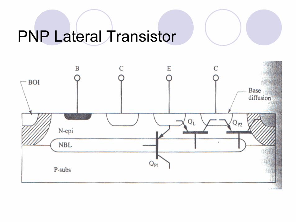

�Major Parasitics�Sidewall saturation
�Avalanche breakdown
�Leakage
�Capacitance between junctions


�Diodes characterize�Capacitance�Avalanche breakdown
�Resistors show internal resistances�Rb is normally quite large�Re is negligible

�Low Rb�Higher frequency operation
�Low Rc�Higher saturation voltages�Power applications for high current

SaturationEbers-Moll Model
Equivalent circuit for the Ebers-Moll model of an NPN bipolarjunction transistor

��������� ���� ������������
FFRC
RRFFB
RRFE
IIIIII
III
�
��
�
���
����
��
)1()1(
The Ebers-Moll parameters are relatedby the following equation
RsCFsE II �� ,, �

�This relationship is also referred as thereciprocity relation. It can be derived byexamining the minority carrier currentthrough the base. For the specific casewhere the base-emitter and base-collectorvoltages are the same and the basedoping is uniform, there can be no minoritycarrier diffusion in the base

�The saturation currents IE,s and IC,s areobtained by measuring the base-emitter(base-collector) diode saturation currentwhile shorting the base-collector (base-emitter) diode.
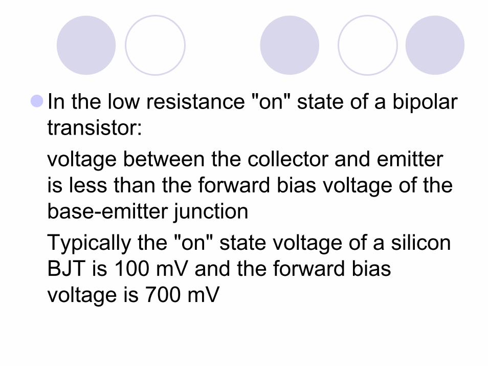
� In the low resistance "on" state of a bipolartransistor:
voltage between the collector and emitteris less than the forward bias voltage of thebase-emitter junction
Typically the "on" state voltage of a siliconBJT is 100 mV and the forward biasvoltage is 700 mV
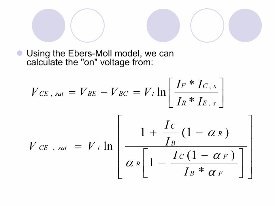
� Using the Ebers-Moll model, we cancalculate the "on" voltage from:
��
���
����
sER
sCFtBCBEsatCE
IIIIVVVV
,
,,
**ln
����
�
�
����
�
�
��
���
� ��
��
FB
FCR
RB
C
tsatCE
II
II
VV
�
�
�
�
*)1(1
)1(1ln,
notes
� Saturation implies that a large amount of minority carrier charge isaccumulated in the base region. As a transistor is switched fromsaturation to cutoff, the charge initially remains in the bas and thecollector current will remain until this charge is removed byrecombination.
� Two techniques are used to reduce the turnoff delay:� 1. adding a schottky diode in parallel to the base collector junction� 2. using an emitter coupled circuit configuration
� Both approaches avoid biasing the transistor in the saturation mode The Schottky diode clamps the base-collector voltage at a value,
which is slightly lower than the turn-on voltage of the base-collectordiode. An emitter-coupled circuit is biased with a current source,which can be designed so that the collector voltage cannot be lessthan the base voltage.

� Calculate the saturation voltage of a bipolartransistor biased with a base current of 1 mAand a collector current of 10 mA. Use aR = 0.993and aF = 0.2.