Embed Size (px)
Citation preview
BNGA Best Practices – 51030001, Rev. C
Page 1 of 14 10/1/2007
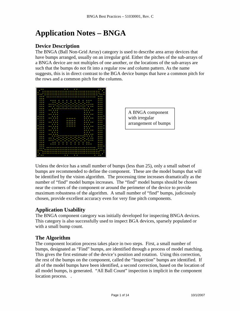
Application Notes – BNGA Device Description The BNGA (Ball Non-Grid Array) category is used to describe area array devices that have bumps arranged, usually on an irregular grid. Either the pitches of the sub-arrays of a BNGA device are not multiples of one another, or the locations of the sub-arrays are such that the bumps do not fit into a regular row and column pattern. As the name suggests, this is in direct contrast to the BGA device bumps that have a common pitch for the rows and a common pitch for the columns.
Unless the device has a small number of bumps (less than 25), only a small subset of bumps are recommended to define the component. These are the model bumps that will be identified by the vision algorithm. The processing time increases dramatically as the number of “find” model bumps increases. The “find” model bumps should be chosen near the corners of the component or around the perimeter of the device to provide maximum robustness of the algorithm. A small number of “find” bumps, judiciously chosen, provide excellent accuracy even for very fine pitch components. Application Usability The BNGA component category was initially developed for inspecting BNGA devices. This category is also successfully used to inspect BGA devices, sparsely populated or with a small bump count. The Algorithm The component location process takes place in two steps. First, a small number of bumps, designated as “Find” bumps, are identified through a process of model matching. This gives the first estimate of the device’s position and rotation. Using this correction, the rest of the bumps on the component, called the “Inspection” bumps are identified. If all of the model bumps have been identified, a second correction, based on the location of all model bumps, is generated. “All Ball Count” inspection is implicit in the component location process. .
A BNGA component with irregular arrangement of bumps
BNGA Best Practices – 51030001, Rev. C
Page 2 of 14 10/1/2007
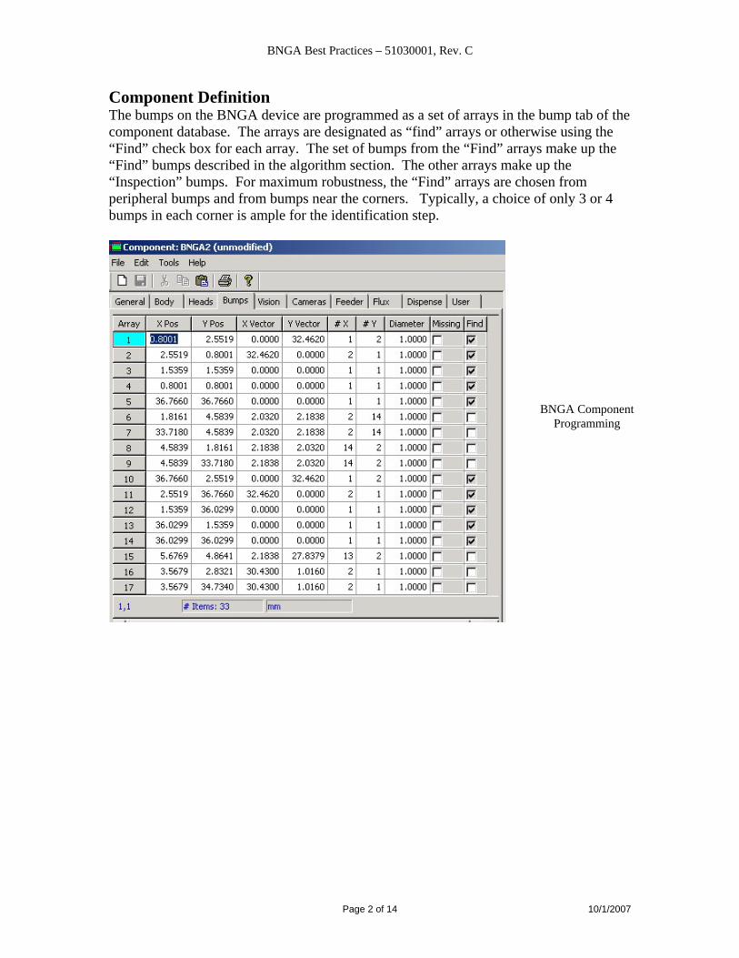
Component Definition The bumps on the BNGA device are programmed as a set of arrays in the bump tab of the component database. The arrays are designated as “find” arrays or otherwise using the “Find” check box for each array. The set of bumps from the “Find” arrays make up the “Find” bumps described in the algorithm section. The other arrays make up the “Inspection” bumps. For maximum robustness, the “Find” arrays are chosen from peripheral bumps and from bumps near the corners. Typically, a choice of only 3 or 4 bumps in each corner is ample for the identification step.
BNGA Component Programming
BNGA Best Practices – 51030001, Rev. C
Page 3 of 14 10/1/2007
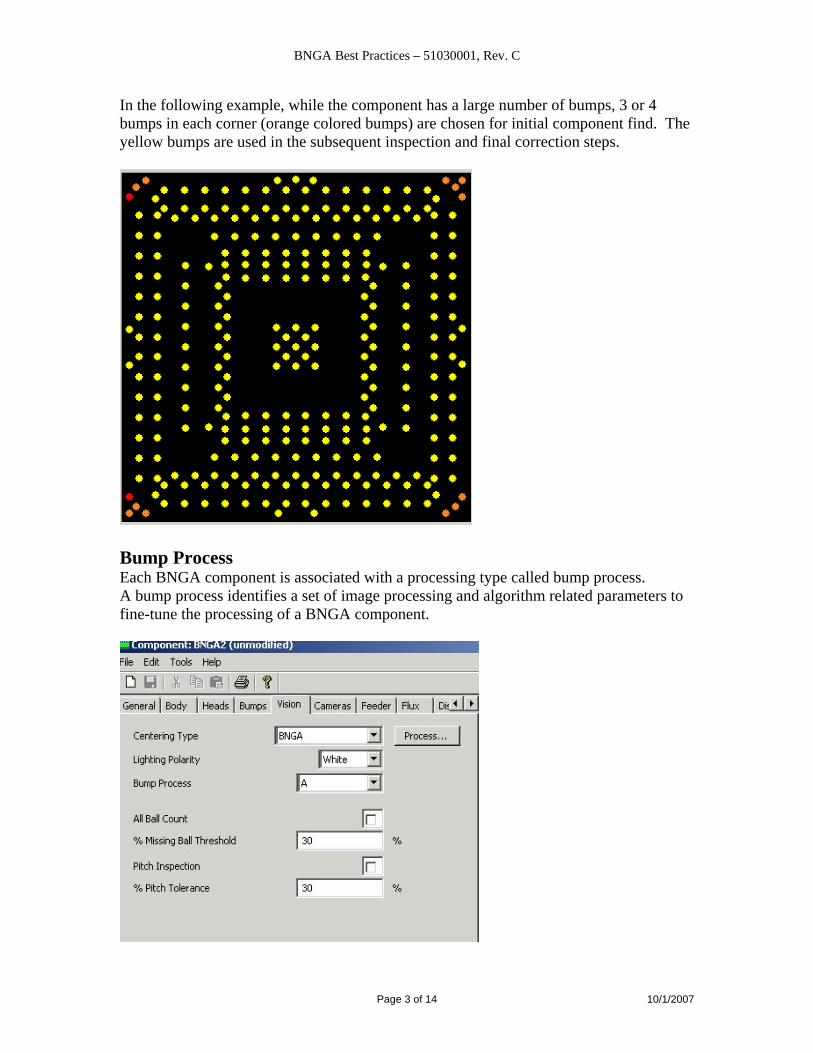
In the following example, while the component has a large number of bumps, 3 or 4 bumps in each corner (orange colored bumps) are chosen for initial component find. The yellow bumps are used in the subsequent inspection and final correction steps.
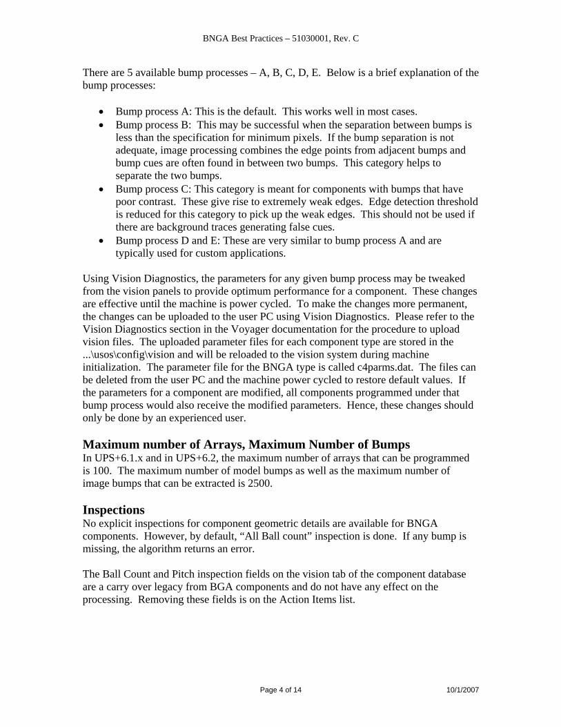
Bump Process Each BNGA component is associated with a processing type called bump process. A bump process identifies a set of image processing and algorithm related parameters to fine-tune the processing of a BNGA component.
BNGA Best Practices – 51030001, Rev. C
Page 4 of 14 10/1/2007
There are 5 available bump processes – A, B, C, D, E. Below is a brief explanation of the bump processes:
• Bump process A: This is the default. This works well in most cases. • Bump process B: This may be successful when the separation between bumps is
less than the specification for minimum pixels. If the bump separation is not adequate, image processing combines the edge points from adjacent bumps and bump cues are often found in between two bumps. This category helps to separate the two bumps.
• Bump process C: This category is meant for components with bumps that have poor contrast. These give rise to extremely weak edges. Edge detection threshold is reduced for this category to pick up the weak edges. This should not be used if there are background traces generating false cues.
• Bump process D and E: These are very similar to bump process A and are typically used for custom applications.
Using Vision Diagnostics, the parameters for any given bump process may be tweaked from the vision panels to provide optimum performance for a component. These changes are effective until the machine is power cycled. To make the changes more permanent, the changes can be uploaded to the user PC using Vision Diagnostics. Please refer to the Vision Diagnostics section in the Voyager documentation for the procedure to upload vision files. The uploaded parameter files for each component type are stored in the ...\usos\config\vision and will be reloaded to the vision system during machine initialization. The parameter file for the BNGA type is called c4parms.dat. The files can be deleted from the user PC and the machine power cycled to restore default values. If the parameters for a component are modified, all components programmed under that bump process would also receive the modified parameters. Hence, these changes should only be done by an experienced user. Maximum number of Arrays, Maximum Number of Bumps In UPS+6.1.x and in UPS+6.2, the maximum number of arrays that can be programmed is 100. The maximum number of model bumps as well as the maximum number of image bumps that can be extracted is 2500. Inspections No explicit inspections for component geometric details are available for BNGA components. However, by default, “All Ball count” inspection is done. If any bump is missing, the algorithm returns an error. The Ball Count and Pitch inspection fields on the vision tab of the component database are a carry over legacy from BGA components and do not have any effect on the processing. Removing these fields is on the Action Items list.
BNGA Best Practices – 51030001, Rev. C
Page 5 of 14 10/1/2007
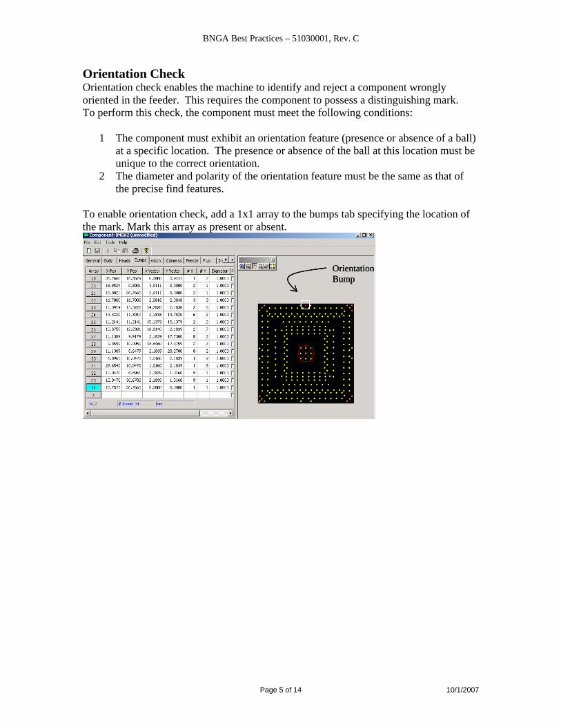
Orientation Check Orientation check enables the machine to identify and reject a component wrongly oriented in the feeder. This requires the component to possess a distinguishing mark. To perform this check, the component must meet the following conditions:
1 The component must exhibit an orientation feature (presence or absence of a ball) at a specific location. The presence or absence of the ball at this location must be unique to the correct orientation.
2 The diameter and polarity of the orientation feature must be the same as that of the precise find features.
To enable orientation check, add a 1x1 array to the bumps tab specifying the location of the mark. Mark this array as present or absent.
Orientation Bump Orientation Bump
BNGA Best Practices – 51030001, Rev. C
Page 6 of 14 10/1/2007
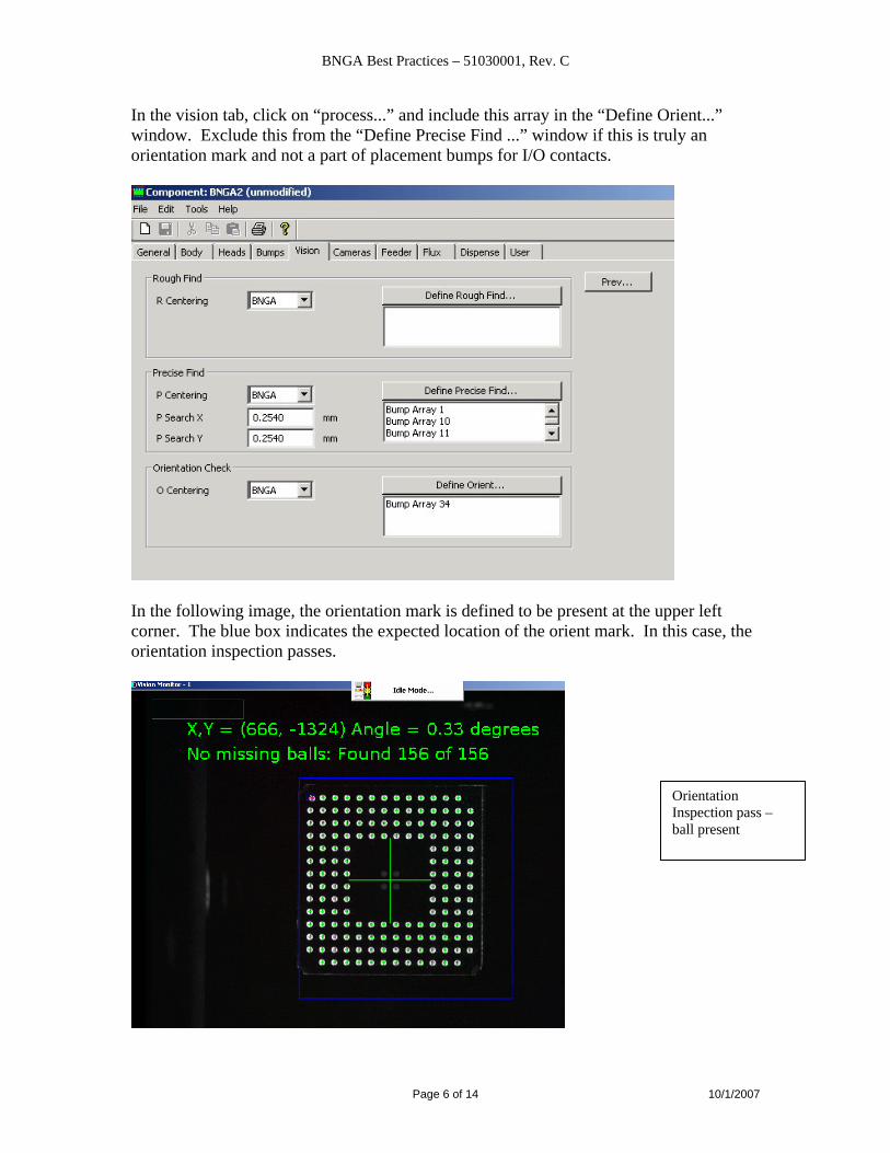
In the vision tab, click on “process...” and include this array in the “Define Orient...” window. Exclude this from the “Define Precise Find ...” window if this is truly an orientation mark and not a part of placement bumps for I/O contacts.
In the following image, the orientation mark is defined to be present at the upper left corner. The blue box indicates the expected location of the orient mark. In this case, the orientation inspection passes.
Orientation Inspection pass – ball present
BNGA Best Practices – 51030001, Rev. C
Page 7 of 14 10/1/2007
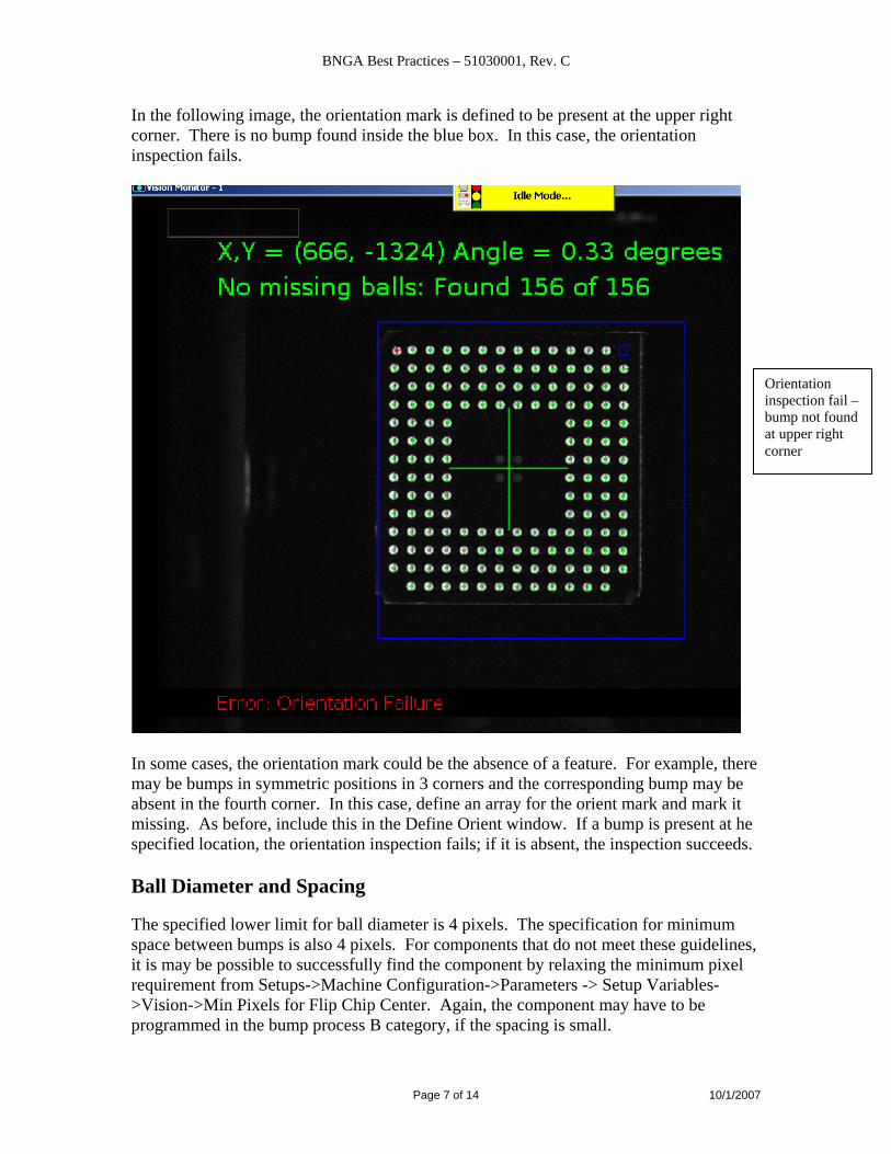
In the following image, the orientation mark is defined to be present at the upper right corner. There is no bump found inside the blue box. In this case, the orientation inspection fails.
In some cases, the orientation mark could be the absence of a feature. For example, there may be bumps in symmetric positions in 3 corners and the corresponding bump may be absent in the fourth corner. In this case, define an array for the orient mark and mark it missing. As before, include this in the Define Orient window. If a bump is present at he specified location, the orientation inspection fails; if it is absent, the inspection succeeds. Ball Diameter and Spacing The specified lower limit for ball diameter is 4 pixels. The specification for minimum space between bumps is also 4 pixels. For components that do not meet these guidelines, it is may be possible to successfully find the component by relaxing the minimum pixel requirement from Setups->Machine Configuration->Parameters -> Setup Variables->Vision->Min Pixels for Flip Chip Center. Again, the component may have to be programmed in the bump process B category, if the spacing is small.
Orientation inspection fail – bump not found at upper right corner
BNGA Best Practices – 51030001, Rev. C
Page 8 of 14 10/1/2007
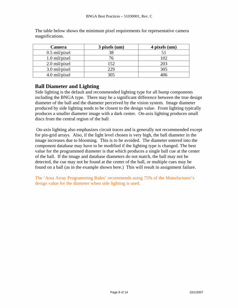
The table below shows the minimum pixel requirements for representative camera magnifications.
Camera 3 pixels (um) 4 pixels (um) 0.5 mil/pixel 38 51 1.0 mil/pixel 76 102 2.0 mil/pixel 152 203 3.0 mil/pixel 229 305 4.0 mil/pixel 305 406
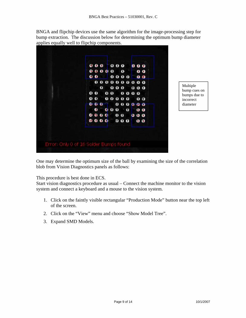
Ball Diameter and Lighting Side lighting is the default and recommended lighting type for all bump components including the BNGA type. There may be a significant difference between the true design diameter of the ball and the diameter perceived by the vision system. Image diameter produced by side lighting tends to be closest to the design value. Front lighting typically produces a smaller diameter image with a dark center. On-axis lighting produces small discs from the central region of the ball. On-axis lighting also emphasizes circuit traces and is generally not recommended except for pin-grid arrays. Also, if the light level chosen is very high, the ball diameter in the image increases due to blooming. This is to be avoided. The diameter entered into the component database may have to be modified if the lighting type is changed. The best value for the programmed diameter is that which produces a single ball cue at the center of the ball. If the image and database diameters do not match, the ball may not be detected, the cue may not be found at the center of the ball, or multiple cues may be found on a ball (as in the example shown here.) This will result in assignment failure. The ‘Area Array Programming Rules’ recommends using 75% of the Manufacturer’s design value for the diameter when side lighting is used.
BNGA Best Practices – 51030001, Rev. C
Page 9 of 14 10/1/2007
BNGA and flipchip devices use the same algorithm for the image-processing step for bump extraction. The discussion below for determining the optimum bump diameter applies equally well to flipchip components.
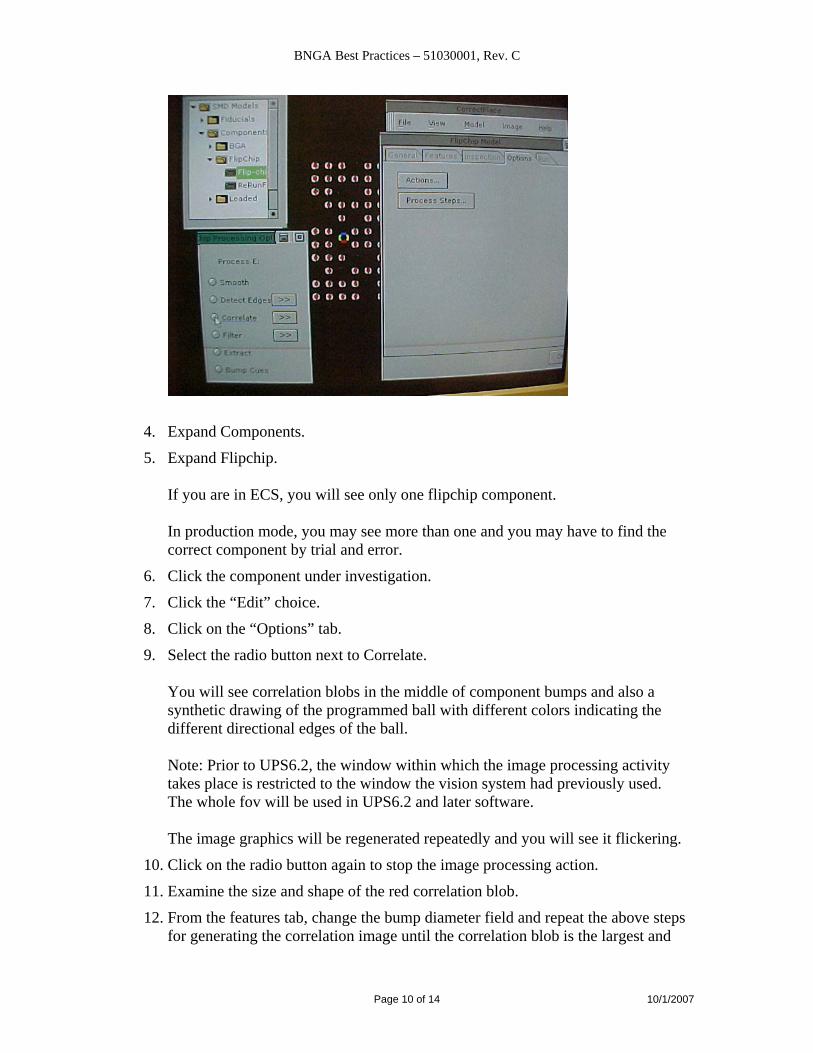
One may determine the optimum size of the ball by examining the size of the correlation blob from Vision Diagnostics panels as follows: This procedure is best done in ECS. Start vision diagnostics procedure as usual – Connect the machine monitor to the vision system and connect a keyboard and a mouse to the vision system.
1. Click on the faintly visible rectangular “Production Mode” button near the top left of the screen.
2. Click on the “View” menu and choose “Show Model Tree”.
3. Expand SMD Models.
Multiple bump cues on bumps due to incorrect diameter
BNGA Best Practices – 51030001, Rev. C
Page 10 of 14 10/1/2007
4. Expand Components.
5. Expand Flipchip. If you are in ECS, you will see only one flipchip component. In production mode, you may see more than one and you may have to find the correct component by trial and error.
6. Click the component under investigation.
7. Click the “Edit” choice.
8. Click on the “Options” tab.
9. Select the radio button next to Correlate. You will see correlation blobs in the middle of component bumps and also a synthetic drawing of the programmed ball with different colors indicating the different directional edges of the ball. Note: Prior to UPS6.2, the window within which the image processing activity takes place is restricted to the window the vision system had previously used. The whole fov will be used in UPS6.2 and later software. The image graphics will be regenerated repeatedly and you will see it flickering.
10. Click on the radio button again to stop the image processing action.
11. Examine the size and shape of the red correlation blob.
12. From the features tab, change the bump diameter field and repeat the above steps for generating the correlation image until the correlation blob is the largest and
BNGA Best Practices – 51030001, Rev. C
Page 11 of 14 10/1/2007
the most spherical. Note that image processing takes place in pixel resolution and you will not see a change until the diameter in pixels (rounded) changes by a whole pixel. Note the best diameter and program it into the component database in USOS.
13. When you are satisfied, click on the “Production Mode” button again to close the GUI. Otherwise, the machine will not take a new picture.
14. You may repeat this process by changing camera lighting and acquiring a new image.
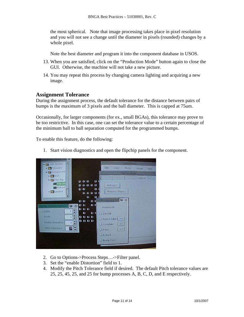
Assignment Tolerance During the assignment process, the default tolerance for the distance between pairs of bumps is the maximum of 3 pixels and the ball diameter. This is capped at 75um. Occasionally, for larger components (for ex., small BGAs), this tolerance may prove to be too restrictive. In this case, one can set the tolerance value to a certain percentage of the minimum ball to ball separation computed for the programmed bumps. To enable this feature, do the following:
1. Start vision diagnostics and open the flipchip panels for the component.
2. Go to Options->Process Steps…->Filter panel. 3. Set the “enable Distortion” field to 1. 4. Modify the Pitch Tolerance field if desired. The default Pitch tolerance values are
25, 25, 45, 25, and 25 for bump processes A, B, C, D, and E respectively.
BNGA Best Practices – 51030001, Rev. C
Page 12 of 14 10/1/2007
5. The Distortion feature is turned off by default. If it is turned on for a component, it will be applicable to all components programmed in that bump process category. The Distortion feature is to be used with caution.
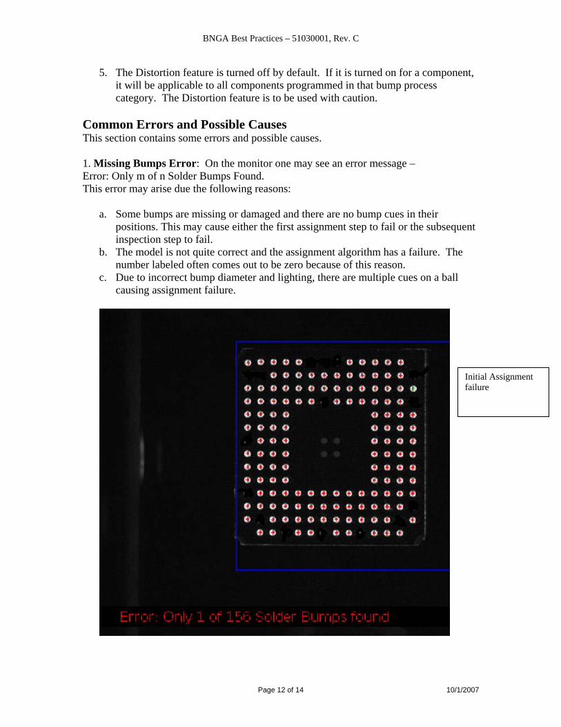
Common Errors and Possible Causes This section contains some errors and possible causes. 1. Missing Bumps Error: On the monitor one may see an error message – Error: Only m of n Solder Bumps Found. This error may arise due the following reasons:
a. Some bumps are missing or damaged and there are no bump cues in their
positions. This may cause either the first assignment step to fail or the subsequent inspection step to fail.
b. The model is not quite correct and the assignment algorithm has a failure. The number labeled often comes out to be zero because of this reason.
c. Due to incorrect bump diameter and lighting, there are multiple cues on a ball causing assignment failure.
Initial Assignment failure
BNGA Best Practices – 51030001, Rev. C
Page 13 of 14 10/1/2007
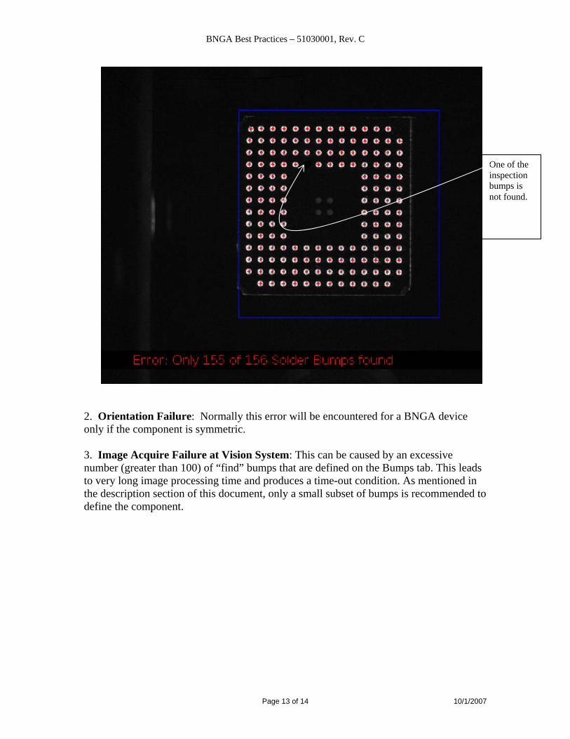
2. Orientation Failure: Normally this error will be encountered for a BNGA device only if the component is symmetric. 3. Image Acquire Failure at Vision System: This can be caused by an excessive number (greater than 100) of “find” bumps that are defined on the Bumps tab. This leads to very long image processing time and produces a time-out condition. As mentioned in the description section of this document, only a small subset of bumps is recommended to define the component.
One of the inspection bumps is not found.
BNGA Best Practices – 51030001, Rev. C
Page 14 of 14 10/1/2007
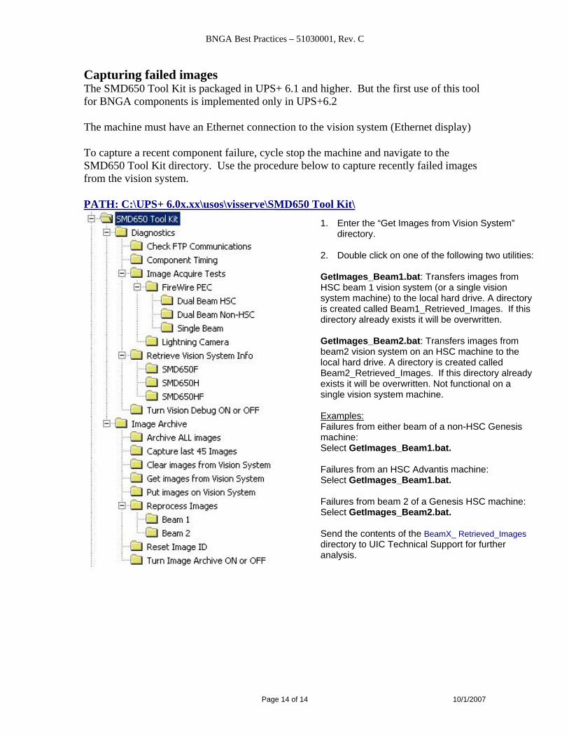
Capturing failed images The SMD650 Tool Kit is packaged in UPS+ 6.1 and higher. But the first use of this tool for BNGA components is implemented only in UPS+6.2 The machine must have an Ethernet connection to the vision system (Ethernet display) To capture a recent component failure, cycle stop the machine and navigate to the SMD650 Tool Kit directory. Use the procedure below to capture recently failed images from the vision system. PATH: C:\UPS+ 6.0x.xx\usos\visserve\SMD650 Tool Kit\
1. Enter the “Get Images from Vision System” directory.
2. Double click on one of the following two utilities: GetImages_Beam1.bat: Transfers images from HSC beam 1 vision system (or a single vision system machine) to the local hard drive. A directory is created called Beam1_Retrieved_Images. If this directory already exists it will be overwritten. GetImages_Beam2.bat: Transfers images from beam2 vision system on an HSC machine to the local hard drive. A directory is created called Beam2_Retrieved_Images. If this directory already exists it will be overwritten. Not functional on a single vision system machine. Examples: Failures from either beam of a non-HSC Genesis machine: Select GetImages_Beam1.bat. Failures from an HSC Advantis machine: Select GetImages_Beam1.bat. Failures from beam 2 of a Genesis HSC machine: Select GetImages_Beam2.bat. Send the contents of the BeamX_ Retrieved_Images directory to UIC Technical Support for further analysis.


