Embed Size (px)
Citation preview

Pb-Free Workshop © Ronald C. Lasky, Timothy Jensen 2003
Implementing Pb-Free Assembly at Your Factory
Ronald C. Lasky, Ph.D., PESenior Technologist Indium Corp
Visiting Professor, DartmouthTimothy Jensen
Indium CorpFeb 2004

Slide #1 Pb-Free Workshop © Ronald C. Lasky, Timothy Jensen 2003
Agenda• Pb-Free World Status• Alloy Selection• Getting Your Facility Ready: Best Practices• PWB and Component Finishes• Solder Paste Pre-Screening• Overview of Motorola Implementation• Large Board and Wave Soldering Issues
All slides available at www.pb-free.com

Slide #2 Pb-Free Workshop © Ronald C. Lasky, Timothy Jensen 2003
Dr. Ron Lasky• Native of Binghamton• Graduate of BCC, Cornell,
BU, Cornell– PhD in materials science
• NYS Professional Engineer• More than 20 years in
electronic and optoelectronic packaging at IBM, Universal Instruments, Cookson(Alpha)
• Author of 5 books• Currently a Senior
Technologist for Indium and a Visiting Professor at Dartmouth College

Slide #3 Pb-Free Workshop © Ronald C. Lasky, Timothy Jensen 2003
Electronics: Still the Largest Industry
• Holding at $1 trillion– Bigger than automotive– But Food?
• $170/yr x 6 billion > $1 T
• Typical long term growth is 6-8% CAGR– Vs 2-4 % for economies in good times– Early 2000s down slightly
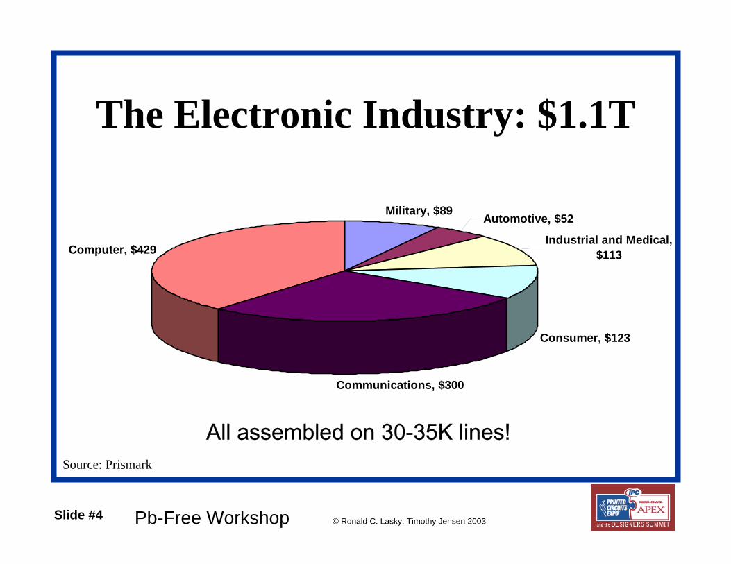
Slide #4 Pb-Free Workshop © Ronald C. Lasky, Timothy Jensen 2003
All assembled on 30-35K lines!
The Electronic Industry: $1.1T
Military, $89 Automotive, $52
Industrial and Medical, $113
Consumer, $123
Communications, $300
Computer, $429
Source: Prismark

Slide #5 Pb-Free Workshop © Ronald C. Lasky, Timothy Jensen 2003
Courtesy Prismark
Slide #6 Pb-Free Workshop © Ronald C. Lasky, Timothy Jensen 2003
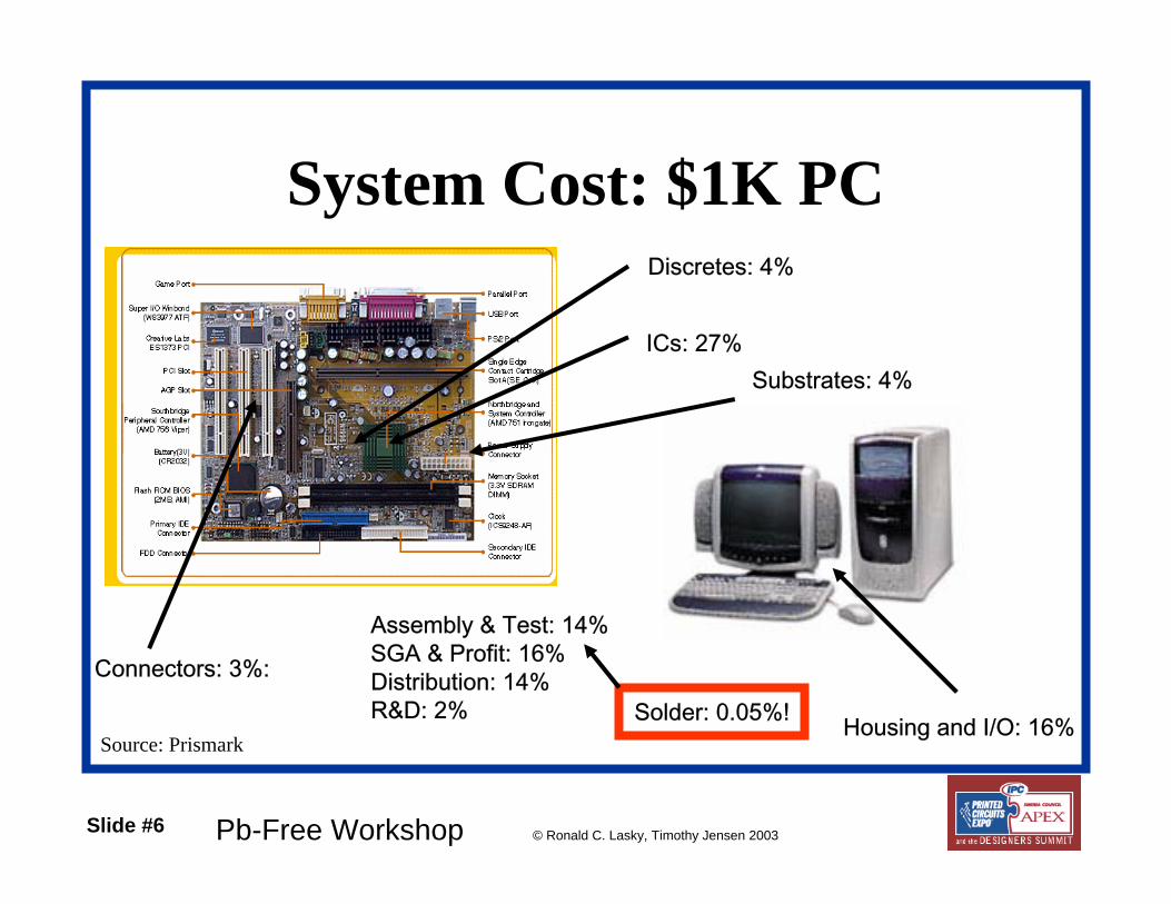
System Cost: $1K PC
Connectors: 3%:
Housing and I/O: 16%
Discretes: 4%
ICs: 27%
Assembly & Test: 14%SGA & Profit: 16%Distribution: 14%R&D: 2%
Substrates: 4%
Solder: 0.05%!Source: Prismark

Slide #7 Pb-Free Workshop © Ronald C. Lasky, Timothy Jensen 2003
What is a Printed Circuit Board (PCB)?• Starts with a PWB• Solder Paste is printed• IC, passive, active
components are placed
• Reflow melts the solder• The finished PCB is
tested• Thru hole assembly may
also be performed
Source: The Internet

Slide #8 Pb-Free Workshop © Ronald C. Lasky, Timothy Jensen 2003
Cross Section of a PQFP Component
The silicon die is the heart of electronics, it produces all ofdigital and analog functions. The material and leads that enclose the die are called the package. The resulting device called a component, a component package or a semiconductorpackage.
Courtesy:Prismark
1.2 centsper lead
Silicon DieMolding CompoundNitto Denko
8 cents
Wire BondedTanaka
18 cents
LeadframeShinko
91 cents
Die Attach AdhesiveAblestik0.4 cents
1.2 centsper lead
Silicon DieMolding CompoundNitto Denko
8 cents
Wire BondedTanaka
18 cents
LeadframeShinko
91 cents
Die Attach AdhesiveAblestik0.4 cents

Slide #9 Pb-Free Workshop © Ronald C. Lasky, Timothy Jensen 2003
• The relentless size reduction of passives
• Assembling the 0201 is one of the current process challenges
• A trillion assembled each year
Source: The Internet

Slide #10 Pb-Free Workshop © Ronald C. Lasky, Timothy Jensen 2003
PWB Assembly
Pick and Place
Reflow OvenChip Shooter
Hand Mount and OptoWave or Selective
SolderInspection/Test
Stencil Printer
Sources: DEK, UIC, Electrovert

Pb-Free Workshop © Ronald C. Lasky, Timothy Jensen 2003
Pb-free Initiatives & Global Trends

Slide #12 Pb-Free Workshop © Ronald C. Lasky, Timothy Jensen 2003
Current Pb-free Legislation
• WEEE/ROHS directives
• Japanese Home Electronics Recycling Law
• USA? Some state activity, nothing federal– EPA: ‘Deal with Electronics or We Will’

Slide #13 Pb-Free Workshop © Ronald C. Lasky, Timothy Jensen 2003
Pb-free Legislation• EU Ratifies WEEE / ROHS directive
– Dec 2002 EU parliament passed legislation to ban use of:
• Pb, Hg, Cd, Cr VI, PBB, PBDE– Affects ALL products sold after July 2006.
• Exceptions– Telecom equipment until 2010– High lead solder applications (>85% lead alloy)
– Recycling program enforced June 2005.

Slide #14 Pb-Free Workshop © Ronald C. Lasky, Timothy Jensen 2003
Pb-free Legislation• Japanese Pb-free Activity
– No direct ban on using Pb– MITI proposed recycling legislation in May 1998.– Japan home electronics recycling law requires
OEMs to collect and recycle 4 major products since April 2001.
– These measures, as well as marketing advantage, are pushing major Japanese companies to be more environmentally conscience

Slide #15 Pb-Free Workshop © Ronald C. Lasky, Timothy Jensen 2003
Japanese Pb-free Products
• Matsushita / Panasonic announcement– By March 2003 – Over 70 million PCBs
(approximately 12,000 product models) will be built using a Pb-free solder.
• Products have been built in over 100 different factories

Slide #16 Pb-Free Workshop © Ronald C. Lasky, Timothy Jensen 2003
MJ70 Minidisc Player MJ30 Minidisc Player
Panasonic Pb-Free Examples

Slide #17 Pb-Free Workshop © Ronald C. Lasky, Timothy Jensen 2003
H845L Camcorder PC Audio Board, Flora 220CX
Hitachi Pb-Free Examples

Pb-Free Workshop © Ronald C. Lasky, Timothy Jensen 2003
Is Pb-Free a good thing?

Slide #19 Pb-Free Workshop © Ronald C. Lasky, Timothy Jensen 2003
True or False
• Electronics is a major contributor to environmental lead. ⇒FALSE
– Batteries: 4,000,000 tons– Bullets: 200,000 tons– Electronics: 18,500 tons < 0.5%– Not to mention tire balancing weights!
• About 100,000 tons/year

Slide #20 Pb-Free Workshop © Ronald C. Lasky, Timothy Jensen 2003
True or False
• The level of lead in the blood of US residents has increased since 1945 ⇒ FALSE
• Paint and gasoline reductions have had a stunningly positive effect.

Slide #21 Pb-Free Workshop © Ronald C. Lasky, Timothy Jensen 2003
Average US Lead Levels in Micrograms per Deciliter of Blood
0
5
10
15
20
25
30
1940 1945 1950 1955 1960 1965 1970 1975 1980 1985 1990 1995
Year
Pb( µ
g/dl
)

Slide #22 Pb-Free Workshop © Ronald C. Lasky, Timothy Jensen 2003
Pb does Leach• Pb Leach Testing
– Use water with a pH of 7-7.05– Pb will not leach very much at this pH
• In acid water, Pb does leach• After all, we banned Pb from
plumbing for good reason• However, no measurable results in a
“real life” experiment

Slide #23 Pb-Free Workshop © Ronald C. Lasky, Timothy Jensen 2003
Pb-Free Solder Alloys
• Present alloys chosen to replace Sn/Pb are Sn/Ag/Cu alloys
• Ag-containing Solders also Leach – EPA Groundwater Leaching Tests
• ALL Pb-free silver-containing solders fail– “Lead-free Solders: A Push in the Wrong Direction?”
Ed Smith, K-Tec Inc.– “Reliability & Leachate Testing of Pb-free Solder
Joints” – Thomas Woodrow, Boeing

Slide #24 Pb-Free Workshop © Ronald C. Lasky, Timothy Jensen 2003
Pb-Free Solder Alloys
• Silver containing replacements – Are we taking a wrong turn?
• Silver is toxic• Silver is a biocide• Silver is known to kill more than 650 different viral,
bacterial and fungal organisms• Also, Silver will kill most marine life
Slide #25 Pb-Free Workshop © Ronald C. Lasky, Timothy Jensen 2003
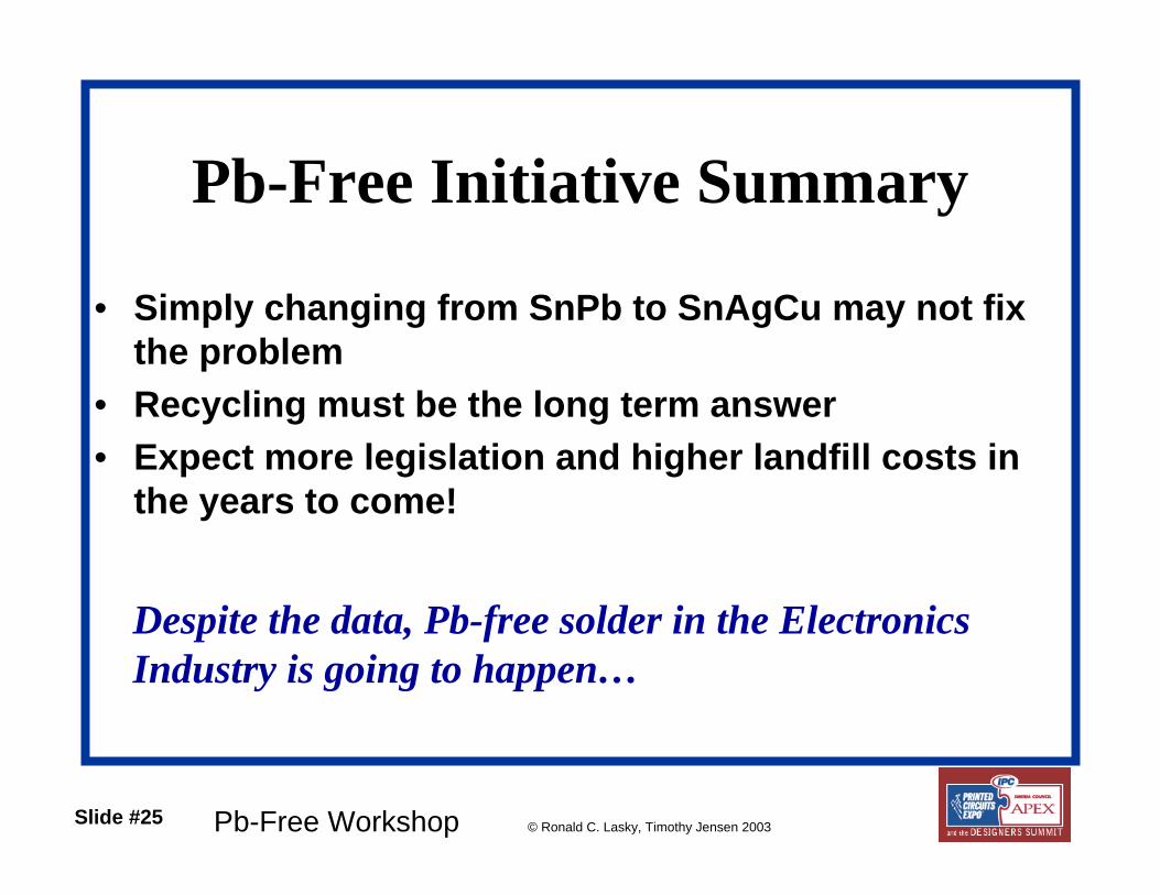
Pb-Free Initiative Summary
• Simply changing from SnPb to SnAgCu may not fix the problem
• Recycling must be the long term answer• Expect more legislation and higher landfill costs in
the years to come!
Despite the data, Pb-free solder in the Electronics Industry is going to happen…

Pb-Free Workshop © Ronald C. Lasky, Timothy Jensen 2003
Pb-Free Alloy Selection

Slide #27 Pb-Free Workshop © Ronald C. Lasky, Timothy Jensen 2003
Alloy Selection Overview
• Potential Alloy Overview• General Alloy Search• Sn/Ag/Cu in Depth

Slide #28 Pb-Free Workshop © Ronald C. Lasky, Timothy Jensen 2003
Alloy Decision Process• The melting point should be as close to
Sn/Pb eutectic as possible• The alloy must be eutectic or very close to
eutectic• It must contain no more than three
elements• Use of existing patents should be avoided
to ease implementation• Reliability should be equal or better than
Sn/Pb Edwin Bradley – NEMI chairperson, Motorola

Slide #29 Pb-Free Workshop © Ronald C. Lasky, Timothy Jensen 2003
Options
• Current Alloy List• Alloy properties• Pros & Cons of each

Slide #30 Pb-Free Workshop © Ronald C. Lasky, Timothy Jensen 2003
Options: Current Alloy List
– Sn/Ag– Sn/Cu– Sn/Ag/Cu– Sn/Ag/Cu/Sb
– Sn/Ag/Bi/X– Sn/Sb– Sn/Zn– Sn/Bi

Slide #31 Pb-Free Workshop © Ronald C. Lasky, Timothy Jensen 2003
Options: Current Alloy List
– Sn/Ag– Sn/Cu– Sn/Ag/Cu– Sn/Ag/Cu/Sb
– Sn/Ag/Bi/X– Sn/Sb– Sn/Zn– Sn/Bi

Slide #32 Pb-Free Workshop © Ronald C. Lasky, Timothy Jensen 2003
Scientific Realities: 91Sn/9Zn• Melting point = 199°C• Zinc reacts with both acids and bases• All flux/vehicles are mildly acidic at room
temperature• Which means shelf-life is in the order of
days, not months!• Also may need conformal coating once in
place - Zn oxidizes very readily

Slide #33 Pb-Free Workshop © Ronald C. Lasky, Timothy Jensen 2003
Scientific Realities: 96.5Sn/3.5Ag• Melting point = 221°C• Years of experience• Relatively poor wetting• Poor thermal cycling (-40/+125)
A1 Sn 3.5Ag 12 12 1282 1987 8A11 Sn 4Ag 1Cu 14 14 2340 2552 3A14 Sn 4Ag 0.5Cu 14 14 2108 2579 5A21 Sn 2.5Ag 0.8Cu 0.5Sb 14 14 2378 2378 2A32 Sn 4.6Ag 1.6Cu 1Sb 1Bi 15 15 2161 2161 4A62 Sn 3.4Ag 1Cu 3.3Bi 14 14 1864 2527 6A66 Sn 3.5Ag 1.5In 14 14 2387 2577 1B63 Sn/Pb Control 13 13 1845 2607 7
Alloy Code Composition Rank# on
Test#
Failed
1st Failure (cycle)
Last Failure (cycle)
Source: NCMS

Slide #34 Pb-Free Workshop © Ronald C. Lasky, Timothy Jensen 2003
Scientific Realities: 58Sn/42Bi• Melting point = 138 °C• Years of experience• Poor shock resistance• 1% Ag addition strengthens this alloy• Low MP eliminates temperature issues
with components and board

Slide #35 Pb-Free Workshop © Ronald C. Lasky, Timothy Jensen 2003
Scientific Realities: Sn/Ag/Cu• Melting Point = 217°C• Cu improves wettability, creep, thermal
fatigue• High solderability & reliability

Slide #36 Pb-Free Workshop © Ronald C. Lasky, Timothy Jensen 2003
Scientific Realities: Sn/Ag/Cu/Sb• Melting point = 215 – 217°C• 0.5% Sb may strengthen alloy• May be considered for wave soldering by
effectively lowering Ag content• Patented composition may limit worldwide
availability• Four part alloy makes manufacturing
consistency less reliable.

Slide #37 Pb-Free Workshop © Ronald C. Lasky, Timothy Jensen 2003
Scientific Realities: Sn/Ag/Bi• Melting Point = 210 - 215 °C• Bi lowers melting point & improves
wettability of SnAg alloys• Avoid using in presence of Pb:
• a 96°C ternary alloy(Sn/Pb/Bi) may form

Slide #38 Pb-Free Workshop © Ronald C. Lasky, Timothy Jensen 2003
Pb-free Alloy Investigation
• Phase 1: DOE to analyze 10 probable alloy solutions using Sn/Pb as Benchmark
• Phase 2: Optimize flux chemistry

Slide #39 Pb-Free Workshop © Ronald C. Lasky, Timothy Jensen 2003
Alloy Performance Investigation
Alloy Solidus Liquidus
63Sn37Pb 182.1 183.096.5Sn3.5Ag 219.7 220.899.3Sn0.7Cu 225.7 227.0
95.5Sn3.8Ag0.7Cu 216.3 217.593.6Sn4.7Ag1.7Cu 215.9 217.1
96.2Sn2.5Ag0.8Cu0.5Sb 216.9 218.291.7Sn3.5Ag4.8Bi 202.1 215.190.5Sn7.5Bi2Ag 190.6 214.7
58Bi42Sn 136.3 138.595Sn5Sb 238.3 240.3
89Sn8Zn3Bi 190.6 195.4

Slide #40 Pb-Free Workshop © Ronald C. Lasky, Timothy Jensen 2003
Pb-free Alloy Investigation
• 5 Individual studies performed– Wetting– Shelf life– Tack time– Solder Ball– Visual reflow inspection
• Performance ranked 0-10 for each category

Slide #41 Pb-Free Workshop © Ronald C. Lasky, Timothy Jensen 2003
Print paste (offset)
Reflow
Cu pad
Solder bump
Unwetted Cu
70%
spread
R&D Test #1: Wetting

Slide #42 Pb-Free Workshop © Ronald C. Lasky, Timothy Jensen 2003
40%
4
50%
5
70%
7
Wetting Examples

Slide #43 Pb-Free Workshop © Ronald C. Lasky, Timothy Jensen 2003
R&D Test #2: Shelf Life
SLI Description0 Overall instability > 25%2 Overall instability = 20-25%4 Overall instability = 15-20%6 Overall instability = 10-15%8 Overall instability = 5-10%10 Overall instability = 0-5%
Shelf life was based on the percentage change in viscosity over time. The length of the test
was 30 days.

Slide #44 Pb-Free Workshop © Ronald C. Lasky, Timothy Jensen 2003
Time
Tack
00
0 2
86
4
10
R&D Test #3: Tack Stability
Slide #45 Pb-Free Workshop © Ronald C. Lasky, Timothy Jensen 2003
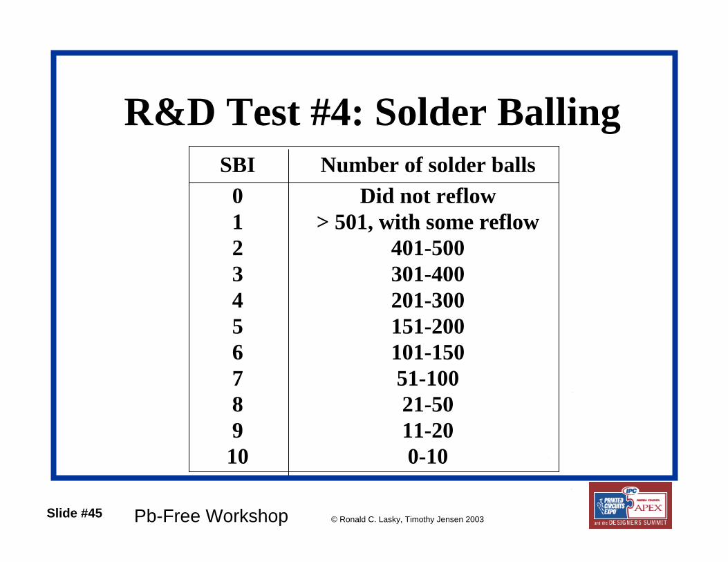
SBI Number of solder balls0 Did not reflow1 > 501, with some reflow2 401-5003 301-4004 201-3005 151-2006 101-1507 51-1008 21-509 11-2010 0-10
R&D Test #4: Solder Balling

Slide #46 Pb-Free Workshop © Ronald C. Lasky, Timothy Jensen 2003
Alloy Investigation- Results
1. Sn63/Pb372. Sn91.7/Bi4.8/Ag3.53. Sn90.5/Bi7.5/Ag24. Sn95.5/Ag3.8/Cu0.75. Sn42/Bi586. Sn93.6/Ag4.7/Cu1.7
7. Sn99.3/Cu0.78. Sn96.2/Ag2.5/Cu0.8/Sb0.59. Sn95/Sb510. Sn96.5/Ag3.511. Sn89/Zn8/Bi3

Slide #47 Pb-Free Workshop © Ronald C. Lasky, Timothy Jensen 2003
BAD
BEST
2
6
10
R&D Test #5: Visual

Slide #48 Pb-Free Workshop © Ronald C. Lasky, Timothy Jensen 2003
Winner- Sn/Ag/Bi ???
• Bi addition lowers melting point & improves wetting
• BUT……..Concerns with• Fillet Lift• Low temperature ternary alloy
formation with Pb contamination

Slide #49 Pb-Free Workshop © Ronald C. Lasky, Timothy Jensen 2003
50
75
100
125
150
175
200
225
250
Sn-3.8Ag-0.7Cu
Sn-2Ag-2Bi Sn-2Ag-4Bi Sn-2Ag-7.5Bi Sn-10.5Bi Sn-12Bi
0%Pb3% Pb6% Pb
Ons
et T
emp,
deg
. C
Sn-Bi-PbPeritectic Sn-Bi-Pb Eutectic
Sn-Pb-AgEutectic
Pb Contamination ConcernsWhy Bi alloys are not the short-term solution

Slide #50 Pb-Free Workshop © Ronald C. Lasky, Timothy Jensen 2003
Ref: Zequn Mei, Fay Hua, and Judy Glazer, “SN- BI- X SOLDERS”, SMTA International, San Jose, CA, Sept. 13- 17, 1999.
Sn/Ag/Bi on Sn/Pb Finish
Sn/Ag/Bi with Pb contamination after 1 reflow
Sn/Ag/Bi with Pb contamination after thermal cycling

Slide #51 Pb-Free Workshop © Ronald C. Lasky, Timothy Jensen 2003
Ref: “Lead-Free Solder Project Final Report”, NCMS Report 0401RE96 , August 1997.
Sn/Ag/Bi Fillet Lift

Slide #52 Pb-Free Workshop © Ronald C. Lasky, Timothy Jensen 2003
Bismuth Alloy Summary
• Sn-Ag-Bi alloys show formation of: – Eutectic 96C phase at Bi > 10.5%Bi– Peritectic 135C phase Bi > 4%Bi
In the presence of Pb.• Sn-Ag-Cu alloys show formation of:
– Eutectic 179C phase.• Wetting occurs at liquidus, so it is key melt
temp variable.• PCB finish can affect wetting temperature due
to base metal diffusion into solder.

Slide #53 Pb-Free Workshop © Ronald C. Lasky, Timothy Jensen 2003
ConclusionPb-free Paste - SnAgCu
• Challenges:– higher processing temperatures– wettability– must wet to a variety of metallizations
Slide #54 Pb-Free Workshop © Ronald C. Lasky, Timothy Jensen 2003
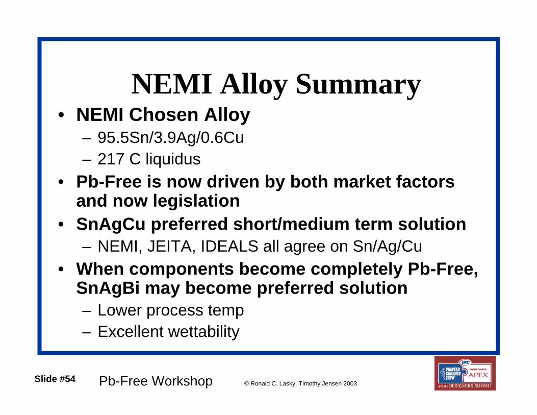
NEMI Alloy Summary• NEMI Chosen Alloy
– 95.5Sn/3.9Ag/0.6Cu– 217 C liquidus
• Pb-Free is now driven by both market factors and now legislation
• SnAgCu preferred short/medium term solution– NEMI, JEITA, IDEALS all agree on Sn/Ag/Cu
• When components become completely Pb-Free, SnAgBi may become preferred solution– Lower process temp– Excellent wettability

Slide #55 Pb-Free Workshop © Ronald C. Lasky, Timothy Jensen 2003
Eutectic of Sn-Ag-Cu soldersB. Boettinger, K. W. Moon of NIST performed studies to determine the true Sn-Ag-Cu eutectic.
Alloys in shaded area have freezing range <10°C.
0 0.5 1 1.5 2 2.5wt% Cu
0
1
2
3
4
5
6
7
8
wt%
Ag
250 C
230 C
270 C
220 C
230 C 270
C
290
C
250
C
230
C
310
C
Estimation of Ternary Liquidus Surface, 10/23/99 Based on Marquette saturation data, with NWU and NIST thermal analysis.
Ag3Sn
Cu6Sn5
SnNIST experimental work showed that the composition is approximately Sn3.5Ag 0.9Cu. (+/- 0.1%) (In agreement with Loomis and Fine)

Slide #56 Pb-Free Workshop © Ronald C. Lasky, Timothy Jensen 2003
Relative Material Costs
• Sn $5.06/kg• Zn $1.06/kg• Cu $1.94/kg• Bi $5.63/kg• In $250.00/kg• Ag $180.00/kg• Sb $1.75/kg• Pb <$1.00/kg

Slide #57 Pb-Free Workshop © Ronald C. Lasky, Timothy Jensen 2003
Pb-Free Cost
• All the lead-free alloys are more expensive than the lead-containing alloys– Raw material costs are higher– Currently there is no economy of scale– Minimal Production experience
compared to Sn/Pb powder production

Slide #58 Pb-Free Workshop © Ronald C. Lasky, Timothy Jensen 2003
Which SAC to Use?
• Melting Point Comparison• Wetting Comparison• Long Term Cost Comparison

Slide #59 Pb-Free Workshop © Ronald C. Lasky, Timothy Jensen 2003
DSC of Actual Samples fromSolder Vendor A
216.67 °C216.54 °C216.65 °CAverage
216.75 °C216.35 °C216.71 °CSample 3
216.56 °C216.38 °C216. 49 °CSample 2
216.70 °C216.89 °C216.76 °CSample 1
95.5Sn/3.8Ag/0.7Cu
95.5Sn/4.0Ag/0.5Cu
96.5Sn/3.0Ag/0.5Cu

Slide #60 Pb-Free Workshop © Ronald C. Lasky, Timothy Jensen 2003
IPC DSC Comparing SAC305 Suppliers
216.0 °C217.25 °C223.45 °CAverage:
216.0 °C216.7 °C220.3 °CSample 2:
216.0 °C217.8 °C226.6 °CSample 1:
Supplier 3Supplier 2Supplier 1
Source: IPC-SPVC-WP-006

Slide #61 Pb-Free Workshop © Ronald C. Lasky, Timothy Jensen 2003
Comparing the Wetting Forces
Difference in wetting per J-STD test procedure not statistically significant between SAC alloys.
Source: IPC-SPVC-WP-006

Slide #62 Pb-Free Workshop © Ronald C. Lasky, Timothy Jensen 2003
SAC Actual Wetting
Source: CEMCEX2003 Seelig et al

Slide #63 Pb-Free Workshop © Ronald C. Lasky, Timothy Jensen 2003
Long Term Relative Costs
• Sn/Pb = 1x• SAC305 = 2.15x • 95.5Sn/3.8Ag/0.7Cu = 2.3x• SAC405 = 2.35x

Slide #64 Pb-Free Workshop © Ronald C. Lasky, Timothy Jensen 2003
Alloy Summary• Sn/Ag/Cu (SAC) is the best current option• Sn/Ag/Bi worth consideration is Pb
contamination is not an issue.• Sn/Bi doped with 1% Ag could be a viable
option for assemblies with tight temperature restrictions.
• SAC305 ranks slightly higher than other SAC alloys due to cost and performance.

Slide #65 Pb-Free Workshop © Ronald C. Lasky, Timothy Jensen 2003
Getting Your Facility Ready: Pb-Free Implementation
Best Practices

Slide #66 Pb-Free Workshop © Ronald C. Lasky, Timothy Jensen 2003
Pb-Free Best Practices• Assess Yourself
– Crucial with Pb-free• Throughput Maximization• CIP• Process Software to Help• Use the Right Tools
– Statistical Thinking– DOE– SPC

Slide #67 Pb-Free Workshop © Ronald C. Lasky, Timothy Jensen 2003
An SMT Process
ActivitiesPeople
Materials
Equipment
Procedures
ProductRequirements
A Product
MeetsRequirements
•On time•Under cost

Slide #68 Pb-Free Workshop © Ronald C. Lasky, Timothy Jensen 2003
Assessment Categories
• DFM, Process and Equipment• Materials Supply and Validation• DOE, SPC, CIP• Training and Failure Analysis• Developed from pooled information
from industry experts

Slide #69 Pb-Free Workshop © Ronald C. Lasky, Timothy Jensen 2003
DFM, Process and EquipmentRanking Key: 0 = strongly disagree or don't know , 3 = disagree, 5= neutral, 7 = agree, 10 = strongly agree
1 10
2 8
3 3
4 9
5 9
6 9
7 9
8 Our process engineers have a disciplined and proven strategy to improve quality: 9
9 3
10 9
Total Score out of 120 98
Ratings:World Class = > 95Above Average = 75 - 94Average = 55 - 74Below Average < 55
Your score places you as "World Class" in DFM, Process and Equipment for SMT assembly. Your clearly recognize the importance of these topics in your assembly processes. This score still offers some opprotunity for improvement. Look at your results on each question and develop an action plan for improvement if appropriate.
The engineer(s) responsible for component placement knows how to balance and optimize the placement equipment. He assures that this operation is performed on all jobs: The engineer in charge of the reflow process assures that the reflow profile matches the solder paste specification:Our process engineers have a disciplined and proven strategy to improve productivity:
Our process equipment is "qualified" with a test and evaluation procedure that is founded on DOE principles:
There is a process engineer or team of engineers responsible for implementing new processes and technology:
We have a documented and functioning DFM system that includes design ground rules (DGRs). Our entire organization is strongly committed to DFM. DFM is a way of life (this question counts 3 times): Our DGRs are established by using designed experiments and statistical process control:
The process engineers know how to run all of the equipment:
The engineer(s) responsible for stencil printing knows how to design a stencil

Slide #70 Pb-Free Workshop © Ronald C. Lasky, Timothy Jensen 2003
Materials Supply and ValidationRanking Key: 0 = strongly disagree or don't know , 3 = disagree, 5= neutral, 7 = agree, 10 = strongly agree
1 0
2 8
3 5
4 7
5 7
6 4
7 4
8 The type (i.e. 2, 3, 4, 5) of the solder paste we use matches the application requirement: 4
9 6
10 6
Total Score out of 120 51
Ratings:World Class = > 95Above Average = 75 - 94Average = 55 - 74Below Average < 55
We evaluate our solder pastes and/or materials with a systematic evaluation procedure, such as "The 12 Board Paste Evaluator" (shown below) or DOE to assure its performance (this question counts 3 times): My engineers have read and understand the solder paste and materials specs and assure they match our use conditions:The response to pause of my solder paste is adequate for my applications:
The cost of my solder paste and/or materials is not the main criteria for its purchase:
Your score places you below average among users of SMT materials. This position offers overwhelming opportunities for improvement. Look at your results on each question and develop an action plan for improvement. Your organization has an urgent need to recognize that evaluating your solder pastes and materials is a most important activity.
The printed volume consistency of my solder paste is best of breed:
My materials supplier(s) understand(s) my process and business needs, we treat each other like partners:
Few, if any end of line defects can be traced to inadequacies of my solder paste and/or materials:
Our organization has a systematic method to assure that the materials/components for future jobs are being prepared while current jobs are being run:Our organization has a systematic method to assure that we have an uninterrupted supply of materials from our vendors:

Slide #71 Pb-Free Workshop © Ronald C. Lasky, Timothy Jensen 2003
DOE, SPC, CIPRanking Key: 0 = strongly disagree or don't know , 3 = disagree, 5= neutral, 7 = agree, 10 = strongly agree
1 3
2 8
3 2
4 2
5 5
6 9
7 9
8 9
9 8
10 8
Total Score out of 120 69
Ratings:World Class = > 95Above Average = 75 - 94Average = 55 - 74Below Average < 55
We measure our unscheduled downtime:
We measure our line efficiency:
Your score places you as average in DOE, SPC and CIP for SMT assembly. This position offers significant opportunities for improvement. Look at your results on each question and develop an action plan for improvement. Having an effective CIP program is vital for success.
We measure our work in process time:
We know our process's Cp and Cpk:
We have a statistical process control program and use the resulting data effectively to monitor and improve our processes:
Quality is everyone's job:
Productivity is everyone's job:
Our process engineers use designed experiments to optimize our processes and evaluate equipment and materials:
We have a continuous improvement plan that is effective, uses metrics, and is recognized as valuable by the entire organization (this question counts 3 times):We measure our process uptime:

Slide #72 Pb-Free Workshop © Ronald C. Lasky, Timothy Jensen 2003
Training and Failure AnalysisRanking Key: 0 = strongly disagree or don't know , 3 = disagree, 5= neutral, 7 = agree, 10 = strongly agree
1 9
2 8
3 5
4 3
5 8
6 4
7 4
8 4
9 6
10 6
Total Score out of 120 75
Ratings:World Class = > 95Above Average = 75 - 94Average = 55 - 74Below Average < 55
Your score places you as above average in Training and Failure Analysis for SMT assembly. This score still offers considerable opportunity for improvement. Look at your results on each question and develop an action plan for improvement, if appropriate.
Our operators cannot change the process equipment's operating parameters:
Our engineers know and use analytical problem solving and brainstorming techniques to perform failure analysis:
There is a process line escalation policy that is understand by all (e.g. if the line is down and remains down this information gets escalated in a documented fashion):
We can perform failure analysis or vend this task out:
Our staff has all ot the tools necessary to perform their jobs:
Our process engineer's yearly performance review is related to process improvement goals:
Our organization has a sophisticated training program for all levels of our staff (this question counts 3 times):
Our engineers understand the difference between common cause and special cause failures and use this knowledge in process troubleshooting:Our engineers use sophisticated modeling tools, like StencilCoach, Reflow Coach and LineBalancer to help them model processes and perform "what if" analysis:Management uses costing tools like ProfitPro to perform financial "what if" analysis, before making financial investments in equipment etc:

Slide #73 Pb-Free Workshop © Ronald C. Lasky, Timothy Jensen 2003
Line Level Metrics Line Efficiency (%) First Pass Yield (%)
20
4060
80100
GoalStart
96
9798
99
100
Goal
Start
9594
Line Uptime (%)
40 50 60 70 80 90 100
WIP (hrs)
7 6 5 4 3 2 1

Slide #74 Pb-Free Workshop © Ronald C. Lasky, Timothy Jensen 2003
But No Matter What You do, Have a CIP
• Assess yourself• Establish/Measure Metrics
– Paste Volume– Productivity Metrics– Pareto Defects
• Monitor Success/Develop Action Plan
• Fix the Problems
Slide #75 Pb-Free Workshop © Ronald C. Lasky, Timothy Jensen 2003
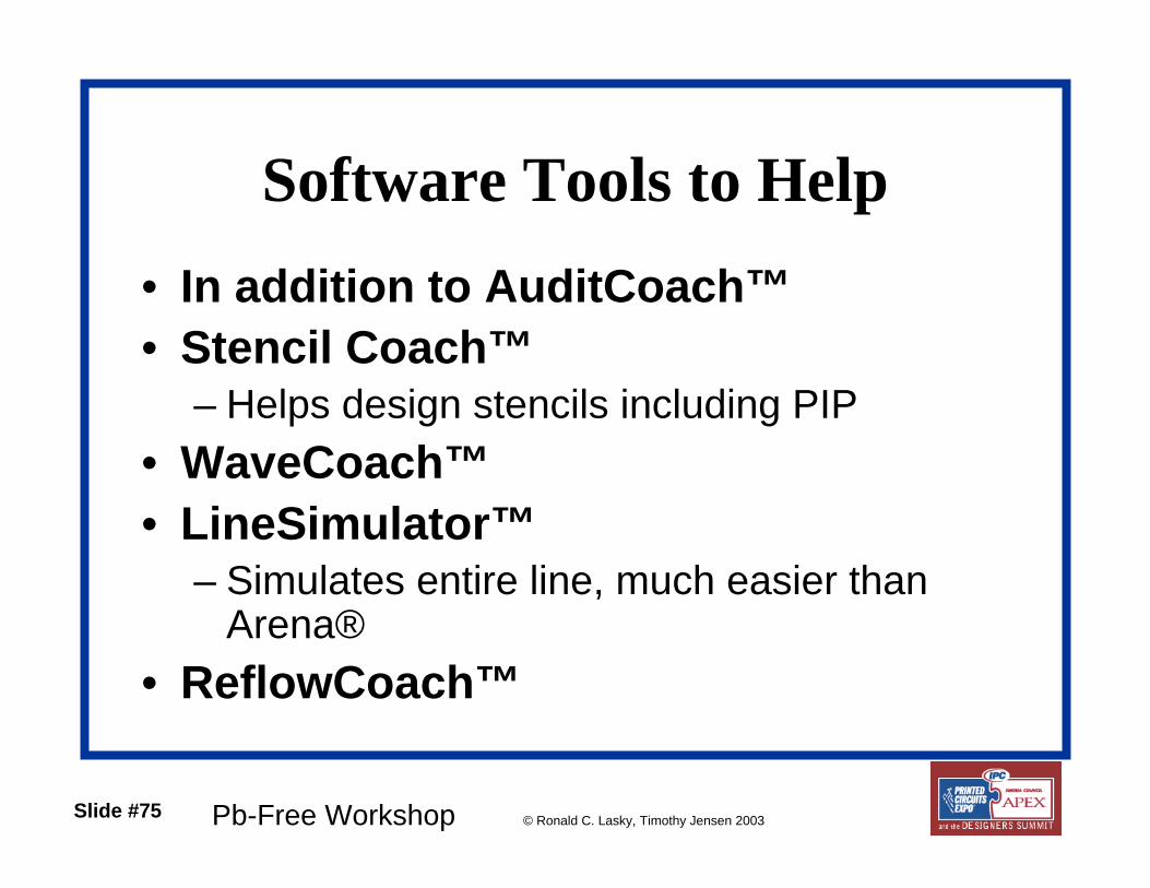
Software Tools to Help• In addition to AuditCoach™• Stencil Coach™
– Helps design stencils including PIP• WaveCoach™• LineSimulator™
– Simulates entire line, much easier than Arena®
• ReflowCoach™

Slide #76 Pb-Free Workshop © Ronald C. Lasky, Timothy Jensen 2003
Stencil Design: StencilCoach™
Calculations Recommendations: PW=1-3+ P/2
W = PW - 2 to 3
AR= W/t > 1.5
Pitch Pad Width PW Aperture W Stencil Aspect ARRectangular Aperatures (P - mils) (PW - mils) OK? (W -mils) OK? Thickness Ratio OK?
(t - mils) (AR)50 26 TRUE 23 TRUE 6 3.833 TRUE 325 15 TRUE 12 TRUE 6 2.000 TRUE 320 12 TRUE 10 TRUE 5 2.000 TRUE 316 10 TRUE 8 TRUE 5 1.600 TRUE 412 8 TRUE 6 TRUE 4 1.500 TRUE 435 19 TRUE 17 TRUE 6 2.833 TRUE 3
Recommendations: PW=0-2+ P/2
D = PW - 2 to 3
ArR=D/4t >0.66
Pitch Pad Dia Pad Dia Aperture D Stencil Area ArRCircular Aperatures (P - mils) (PD - mils) OK? Diameter OK? Thickness Ratio OK?
(D-mils) (t-mils) (ArR)40 21 TRUE 19 TRUE 5 0.95 TRUE 3
Solder Paste Type
Solder Paste Type
Aperture Width > 4-5 particle diameters
Aspect Ratio = W/t > 1.5
Aspect Ratio
t
W
Area Ratio
D
t
Aopening= πD2/4Awall=πDt =>ArR=D/4t
Circular Aperture Diameter > 8 particle diameters
ArR = D/4t > 0.66

Slide #77 Pb-Free Workshop © Ronald C. Lasky, Timothy Jensen 2003
Pin-in-Paste
Inputs OutputsSolder Pad Diameter (mils) 76 V = 2Vf +Vh-Vp Cubic Mils
Pin diameter mils 18 Vf 17585.147PTH diameter mils 30 Vh 40997.784PWB Barrel Length mils 58 Vp 14759.202Paste Reduction Factor 0.52 V 61408.876
Solder Paste Volume Needed 118093.992
If Pin is Square…... Stencil MetricsLength - mils 18 Stencil Thickness - mils 7Width - mils 22 Side: If Square Aperture - mils 129.887Equivalent Pin Dia mils 22.454 Radius: If Round Aperture - mils 73.281
Rectangular? If First Side is (mils): 80Second Side should be (mils: 210.882
Instructions: Tstencil metricscomponent inCells D32-33 aor stencil ape
Vf
Vp
Vh
Vsolder= 2Vf + Vh - Vp
Vf= Fillet Volume (Pappus-Gu
Vh= PWB Hole Volume
Vp= Pin Volume

Slide #78 Pb-Free Workshop © Ronald C. Lasky, Timothy Jensen 2003
Time 265Temp 240
Time-s 0 90 140 190 230 250 295 325Temp-C 30 100 150 209 217 230 217 120
Thruput CalculatorTunnel Length cm 249 Thruput Bds/min 2.84 Obeys Lee Dwell Criteria? YesBelt Speed cm/min 71 Profile Time (min) 3.51Product Length cm 20Product Spacing cm 5
Time
Tem
pera
ture
217
C
ReflowCoachTM

Slide #79 Pb-Free Workshop © Ronald C. Lasky, Timothy Jensen 2003
Ramp Up to 217 C
0
50
100
150
200
250
0 50 100 150 200 250 300 350 400
Time (seconds)
Tem
pera
ture
(C)
Lower LimitUpper LimitUser Profile

Slide #80 Pb-Free Workshop © Ronald C. Lasky, Timothy Jensen 2003
Time Above Liquidus
215
220
225
230
235
240
245
250
255
260
0 20 40 60 80 100
Time (seconds)
Tem
pera
ture
(C)
User ProfileHi RampLow RampTemp MaxTemp MinTime MinTime Max

Slide #81 Pb-Free Workshop © Ronald C. Lasky, Timothy Jensen 2003
Ramp Down
120
130
140
150
160
170
180
190
200
210
220
290 295 300 305 310 315 320 325 330
Time (Seconds)
Tem
pera
ture
(C)
Low RampHi RampUser Profile

Slide #82 Pb-Free Workshop © Ronald C. Lasky, Timothy Jensen 2003
The Tools to Do the Job Right
• Statistical Thinking• DOE• SPC

Slide #83 Pb-Free Workshop © Ronald C. Lasky, Timothy Jensen 2003
ParetosHistograms
CommonCauses
SpecialCauses
ProcessVariation
ControlCharts
Statistical Thinking
Ref: Sheri Flori

Slide #84 Pb-Free Workshop © Ronald C. Lasky, Timothy Jensen 2003
Statistical Thinking…The Case of the Squirrel
• The greatest birder in MA was being harassed by squirrels
• It was a crisis• Even squirrel proof
feeders designed by NASA wouldn’t work
• We needed to apply BMT!

Slide #85 Pb-Free Workshop © Ronald C. Lasky, Timothy Jensen 2003
So I Got Serious
A Crossman BB/Pellet Gun

Slide #86 Pb-Free Workshop © Ronald C. Lasky, Timothy Jensen 2003
X
X
The first shot with BBs.What should I do?

Slide #87 Pb-Free Workshop © Ronald C. Lasky, Timothy Jensen 2003
X
X
The second shot.
X

Slide #88 Pb-Free Workshop © Ronald C. Lasky, Timothy Jensen 2003
X
X
The third shot andfourth.
X
X
X
What is it telling me?

Slide #89 Pb-Free Workshop © Ronald C. Lasky, Timothy Jensen 2003
X
X
I try pellets.
XX
X
What is this telling me?

Slide #90 Pb-Free Workshop © Ronald C. Lasky, Timothy Jensen 2003
Accuracy and Precision• Accuracy: How close
to the measured.• Precision: How
repeatable• Examples of:
– Poor accuracy and precision (BB’s)
– Good precision, poor accuracy (pellets w/ bad sighting)
TargetValue
MeasuredValue
Accuracy
Repeatability(Precision)

Slide #91 Pb-Free Workshop © Ronald C. Lasky, Timothy Jensen 2003
USLLSL
USLLSL
LSL USLProcess Variation = Lost $
Ref: Sheri Flori

Slide #92 Pb-Free Workshop © Ronald C. Lasky, Timothy Jensen 2003
Common Cause• Natural, expected variation• Controllable• What are examples of CC
in calibrating the pellet gun
Special Cause• Unnatural, not expected• Possible examples in pellet gun calibration
Types of Variation
Knob twiddling can correct neither!

Pb-Free Workshop © Ronald C. Lasky, Timothy Jensen 2003
An SMT Electronic Assembly DOE Example

Slide #94 Pb-Free Workshop © Ronald C. Lasky, Timothy Jensen 2003
Score
Random Variation =Variance: Sr
2
Average = 82N
umbe
r of R
ound
s
Random Variation:Dr. Ron Golf Scores

Slide #95 Pb-Free Workshop © Ronald C. Lasky, Timothy Jensen 2003
Tiger’s Scores Dr. Ron
∆= Differencein averages
Implies that there is a greater difference between Tiger and Dr. Ron, than among them ∆2 >> Sr
2
Num
ber o
f Rou
nds
STiger
Variation from Factors: Tiger vs Dr. Ron
SDr. Ron
8268

Slide #96 Pb-Free Workshop © Ronald C. Lasky, Timothy Jensen 2003
For example: Phil Mickelson and David Toms. Then, ∆2 << Sr
2
∆
Num
ber o
f Rou
nds
Score
Sr
When Variation from Factor Change is Small…….

Slide #97 Pb-Free Workshop © Ronald C. Lasky, Timothy Jensen 2003
DOE Uses ANOVA• ANOVA (Analysis of Variance)
РCompares S2 to ƥ The F Statistic:
• Large F => factors have a significant effect on result
• “Large” varies with sample size, typically > 4 for 95% confidence
2
2
rSF ∆
∝

Slide #98 Pb-Free Workshop © Ronald C. Lasky, Timothy Jensen 2003
A Good Stencil Print
*Illustrations courtesy of MPM Corporation

Slide #99 Pb-Free Workshop © Ronald C. Lasky, Timothy Jensen 2003
High Speed UFP Printing
• The objective is to perform High Speed Ultra-Fine Pitch Stencil Printing.
• Print speed, separation speed and wipe frequency need to be minimized to reach this goal.
• Target is 8 second cycle time with current cycle time >20 seconds

Pb-Free Workshop © Ronald C. Lasky, Timothy Jensen 2003
1010
00
55
LOADLOAD SEPARATESEPARATEPRINTPRINTVISIONVISION UNLOADUNLOAD
21.8 sec.
WipeWipe
Cycle Time Breakdown
• 10 inch wide board printed at 1 inch• 2 s Load + 2 s Vision + 10 s Print + 5 s Separate + 1.8 s Unload + 1 s Wipe = 21.8 sec

Pb-Free Workshop © Ronald C. Lasky, Timothy Jensen 2003
1010
00
55
LOAD SEP.PRINTVISION UNLOAD Wipe
Cycle Time Breakdown
Objective:1.8 s Load + 1.8 s Vision + Print + Separate + 1.5 s Unload + Wipe < 8sec

Slide #102 Pb-Free Workshop © Ronald C. Lasky, Timothy Jensen 2003
Factors• A: Print Speed: 1=4, 2=6, 3=8 inch/sec• B: Separation Speed: 1 = 1, 2 = 1.5 sec• C: Wipe Freq: 1= 1/8, 2= 1/12
– 1/8 adds 0.875 sec, 1/12 adds 0.6 secs
• D: Stencil Type: 1= Efab, 2 = Laser• E: Paste: Vendor A =1, Vendor B =2• Full Factorial• Assume no interactions• Aperture: W= 8, t= 5, L= 64 mils=>2560 mils3
• Desire paste volume to be +/- 10% of aperture volume
• Response: Solder Paste Volume
Number of Runs:3x2x2x2x2=48Not that many!

Slide #103 Pb-Free Workshop © Ronald C. Lasky, Timothy Jensen 2003
Source DF Seq SS Adj SS Adj MS F P
Print Sp 2 175117 175117 87558 2.48 0.096
Separati 1 104533 104533 104533 2.97 0.093
Paste Ty 1 559008 559008 559008 15.86 0.000
Stencil 1 274519 274519 274519 7.79 0.008
Wipe Fre 1 902008 902008 902008 25.60 0.000
Error 41 1444731 1444731 35237
Total 47 3459917
For stencil and paste, we can reject H0 with confidence. Hence, we can select
the better choice for each of these factors and re-experiment to optimize total speed.
MiniTab Results
Minitab is available Free for 30 days atMinitab.com!

Slide #104 Pb-Free Workshop © Ronald C. Lasky, Timothy Jensen 2003
SPC and Variables Data
• Data relating to a specific process step
• Quantitative• Can be used to monitor and improve
process performance• Example: Solder Paste Volume• Variables data are crucial for an
effective SPC Plan

Slide #105 Pb-Free Workshop © Ronald C. Lasky, Timothy Jensen 2003
Process Data: Attribute Data• Data that relates to the
performance of the product
• Examples:– Shorts– Opens– Missing Component
• Important, but cannot be measured to improve process performance
• Any plan should strive to relate attribute data to variables data and develop a CIP around this relationship
0
50
100
150
200
250
300
350
Shorts Opens MissingCompnent
Solder Balls
Pareto Attribute Data

Slide #106 Pb-Free Workshop © Ronald C. Lasky, Timothy Jensen 2003
Variables Data Example
Solder Paste Volume Solder Paste Volume
Shor
ts
Ope
ns
Lower Spec LimitUpper Spec Limit
= Average

Slide #107 Pb-Free Workshop © Ronald C. Lasky, Timothy Jensen 2003
Variables Data: Solder Paste Volume
LSL USL
Solder Paste Volume
Proc
ess
Occ
urre
nces
LCL UCL

Slide #108 Pb-Free Workshop © Ronald C. Lasky, Timothy Jensen 2003
Control Chart for SPC
Sigma 3
Sigma 2
Sigma 1
Sigma 1
Sigma 2
Sigma 3
UCL
LCL
Centerline
USL
LSL

Slide #109 Pb-Free Workshop © Ronald C. Lasky, Timothy Jensen 2003
Solder Paste ASolder Paste B

Slide #110 Pb-Free Workshop © Ronald C. Lasky, Timothy Jensen 2003
2001000
1900
1800
1700
1600
Xbar and R Chart
Subgr
Mea
n5
1
5
Mean=1750
UCL=1898
LCL=1602
600
400
200
0
Ran
ge
22
R=255.9
UCL=541.0
LCL=0
200190180
Last 25 Subgroups1950
1800
1650
1500
Subgroup Number
Valu
es
21001400
Capability PlotProcess Tolerance
III
III
IISpecifications
Within
Overall
200017501500
Normal Prob Plot
220017001200
Capability Histogram
WithinStDev:Cp:Cpk:
1101.061.06
OverallStDev:Pp:Ppk:
111.6341.051.05
Process Capability Sixpack for Print VolumePaste B

Slide #111 Pb-Free Workshop © Ronald C. Lasky, Timothy Jensen 2003
2001000
2050
1800
1550
1300
Xbar and R Chart
Subgr
Mea
n
1
1
111
66111
66151111
51
6
11156
11155
1
521
22
1
2222
1
2212
1
2
8
5 6115111
2
15111656
1
15
1
6
1
2
1
1211
11
11
8
165
611
622
1
61
6611
62
11
6
1
6512
1
5
155
1111
5116222
1
2
112
Mean=1750
UCL=1898
LCL=1602
1500
1000
500
0
Ran
ge 1
1
1
111111222
1
1
2
1
211
1
11111
12
1
1
1111
11
2
1
1
21111
2
1
2
1
1211
2
112222111
11111
2
111111
2
111
1
112
1111
21122
122
1111
2
1
11
222
1
22122
1
1
11
111
21
1
112
1
2
1122
1211
2
1
2
11
22222
111
12
1
2
1
21211
11
22
1
2
1
22111
2
1
22
111
212
1
2
11
222112
1
2112
R=255.9
UCL=541.0
LCL=0
200190180
Last 25 Subgroups2500
2000
1500
1000
Subgroup Number
Valu
es
21001400
Capability PlotProcess Tolerance
III
III
IISpecifications
Within
Overall
26001600600
Normal Prob Plot
25001500500
Capability Histogram
WithinStDev:Cp:Cpk:
1101.061.06
OverallStDev:Pp:Ppk:
273.1520.430.43
Process Capability Sixpack for Print VolumePaste A

Slide #112 Pb-Free Workshop © Ronald C. Lasky, Timothy Jensen 2003
Best Practices Summary
• Assess Yourself• Use Metrics• Develop and Implement Action Plan• Monitor Success• Continuously Improve

Slide #113 Pb-Free Workshop © Ronald C. Lasky, Timothy Jensen 2003
Pb-Free Board/Component Finishes
Board Finishes– Immersion Ag– OSP– Electroless Ni/Immersion
Au– Immersion Sn
Component Finishes– Sn/Pb– 100% Sn– Pd/Ag– Ni/Pd– Ni/Sn– Ni/Au– Ni/Pd/AU
Pb Contamination and ability to withstand the higher reflow temperatures are the main concerns.

Slide #114 Pb-Free Workshop © Ronald C. Lasky, Timothy Jensen 2003
Component Finishes: Pure Sn
• Easiest and most obvious choice• Sn Whiskers still a major concern• So TI recommends Ni/Pd/Au

Slide #115 Pb-Free Workshop © Ronald C. Lasky, Timothy Jensen 2003
Structure of PbStructure of Pb--Free Free PreplatedPreplated FinishesFinishes
PALLADIUM: MINIMUM OF 3u”
NICKEL: 40 - 60 u”
Pd / Ni STRIKE: < 5 u”
Ni STRIKE: < 5 u”
COPPER BASE METAL COPPER BASE METAL
NICKEL: 20 - 80 u”
PALLADIUM: 0.2-6.0 u”
GOLD: 30-150 ANGSTROMSNiPd finish: Past
• NiPdAu structure shown has been in use since early 1990s.
• Enhanced wetting performance with NiPdAu finish seen in solderability tests.
• See TI Application Note SZZA026 for complete evaluation of NiPdAu finish.
NiPdAu finish: Present
Courtesy: James Huckabee, TI

Slide #116 Pb-Free Workshop © Ronald C. Lasky, Timothy Jensen 2003
NiPdAuNiPdAu (SOP) Board Mount: Visual Appearance(SOP) Board Mount: Visual Appearance
Visual Appearance Results: All solder joints exhibited a heel fillet height at least one times the lead thickness and evidence of wetting to the sides of the leads. This performance would be considered acceptable for all 3 classes of products identified in IPC-A-610C (general electronic products, dedicated service electronic products, and high performance electronic products.
Typical wetting NiPdAu finished SOP components with SnPbAg solder, NiAuPWB finish.
Typical wetting NiPdAu finished SOP components with SnAgCu solder, NiAuPWB finish.
Courtesy: James Huckabee, TI

Slide #117 Pb-Free Workshop © Ronald C. Lasky, Timothy Jensen 2003
PWB Surface Finish Summary
Hazard to Manufacture
Availability
Cost (To HASL)
Wire Bonding
Contact Connections
Fine pitch quality
Thickness (microinches)
LowHighLowModerateHigh
LimitedVery LimitedHighModerateHigh
1X1X0.3X2X1X
LimitedNot Recommended
Not RecommendedLimitedNot
Recommended
GoodGoodNot RecommendedGoodFair
ExcellentExcellentExcellentExcellentPoor
3 - 1240 – 608 - 20Au: 3 - 8
Ni 50 - 150100 – 1000
ImAgImSnOSPENIGHASL

Slide #118 Pb-Free Workshop © Ronald C. Lasky, Timothy Jensen 2003
2006 Finish Estimations
Projections courtesy of Enthone, Cookson ElectronicsAdditional slides available at www.pb-free.com

Slide #119 Pb-Free Workshop © Ronald C. Lasky, Timothy Jensen 2003
Immersion Ag
• Low Cost• Planar Surface• Compatible with touchpads /
solderless connections (if thicker Ag is used)
• 2 – 10 microinches typical thickness
Additional slides available at www.pb-free.com
Slide #120 Pb-Free Workshop © Ronald C. Lasky, Timothy Jensen 2003
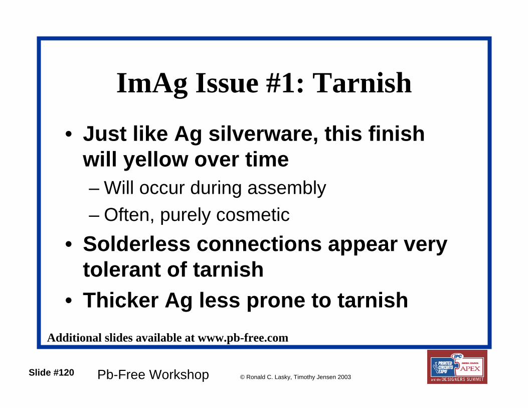
ImAg Issue #1: Tarnish
• Just like Ag silverware, this finish will yellow over time– Will occur during assembly– Often, purely cosmetic
• Solderless connections appear very tolerant of tarnish
• Thicker Ag less prone to tarnishAdditional slides available at www.pb-free.com

Slide #121 Pb-Free Workshop © Ronald C. Lasky, Timothy Jensen 2003
ImAg Issue #2: Migration
• The presence of moisture and current can cause the migration of Ag ions
• Migrate from cathode to anode forming dendrites that reduce resistance…may eventually form a short
Additional slides available at www.pb-free.com

Slide #122 Pb-Free Workshop © Ronald C. Lasky, Timothy Jensen 2003
ImAg Issue #2: Migration
*graph from www.alphametals.com
NO SIGN OF DENDRITIC GROWTH

Slide #123 Pb-Free Workshop © Ronald C. Lasky, Timothy Jensen 2003
ImAg Issue #3: Premature Intermetallic Failure
Additional slides available at www.pb-free.com

Slide #124 Pb-Free Workshop © Ronald C. Lasky, Timothy Jensen 2003
ImAg Issue #3: Premature Intermetallic Failure
• Thick Ag finishes tarnish less and are more compatible with solderlessconnections, but…– Thick Ag means more organic co-deposit– Organic co-deposit must be forced out of
molten solder– Non-expulsion of organics can result in
microvoids along board/solder intermetallicAdditional slides available at www.pb-free.com

Pb-Free Workshop © Ronald C. Lasky, Timothy Jensen 2003
Pb-Free Solder Paste Evaluation: Pre-Screening
Since there are 10-20 solder paste suppliers, it is essential to narrow down the Pb-free candidates prior to actual physical
evaluation

Slide #126 Pb-Free Workshop © Ronald C. Lasky, Timothy Jensen 2003
Lot-to-Lot Viscosity Stability

Slide #127 Pb-Free Workshop © Ronald C. Lasky, Timothy Jensen 2003
Typical Pb Contamination
Pb Content Must be less than 0.05%

Slide #128 Pb-Free Workshop © Ronald C. Lasky, Timothy Jensen 2003
Pb-Free Reliability
• Surface Insulation Resistance– Test procedure in J-STD-004– 7-day test to determine if flux residue with
affect electrical reliability• Electromigration
– Test procedure in Telcordia GR-78– 21-day test for electrochemical migration

Slide #129 Pb-Free Workshop © Ronald C. Lasky, Timothy Jensen 2003
Pb-Free Supplier Support
• Assess your company needs against supplier capabilities.– Are they available globally?– Are they available locally?– Can they accommodate changing
requirements?

Pb-Free Workshop © Ronald C. Lasky, Timothy Jensen 2003
Pb-Free Solder Paste Evaluation: Printing through Reflow
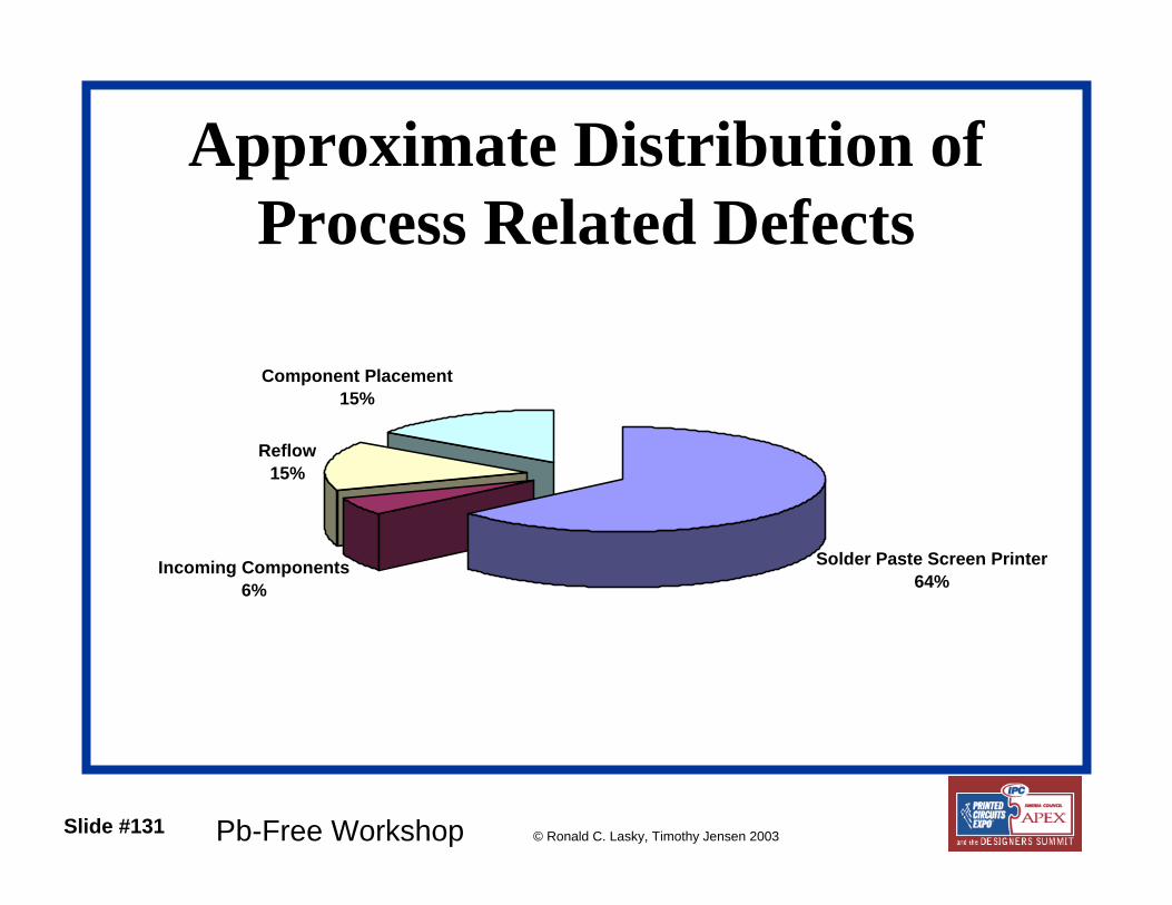
Slide #131 Pb-Free Workshop © Ronald C. Lasky, Timothy Jensen 2003
Solder Paste Screen Printer64%
Incoming Components6%
Reflow15%
Component Placement15%
Approximate Distribution of Process Related Defects

Slide #132 Pb-Free Workshop © Ronald C. Lasky, Timothy Jensen 2003
Evaluating the Pb-Free Print Process: Four Main Paste Variables
• Viscosity Relative to Production Temperature
• Stencil Life• Response to Pause• Resistance to Excessive Shear
Thinning

Slide #133 Pb-Free Workshop © Ronald C. Lasky, Timothy Jensen 2003
Effects of ViscosityToo High
• Poor rolling• Blade Hang-up• Aperture clogging• Insufficients
Too Low
• Excessive deposit• Solder balling• Solder beading• Slumping• Bridging

Slide #134 Pb-Free Workshop © Ronald C. Lasky, Timothy Jensen 2003
Viscosity Vs. Temperature

Slide #135 Pb-Free Workshop © Ronald C. Lasky, Timothy Jensen 2003
Inspired by: MPM
Solder Paste Stencil LifeTack Life
-6
-5
-4
-3
-2
-1
0
1
2
3
4
0 5 10 15 20 25 30
Time (hrs)
Del
ta T
ack
Forc
e (g
ram
s/m
m2)
Brand XGood Paste

Slide #136 Pb-Free Workshop © Ronald C. Lasky, Timothy Jensen 2003
Effects of Short Stencil Life
• Variability in solder paste deposits• Loss of “up time”• Wasted paste, wasted money

Slide #137 Pb-Free Workshop © Ronald C. Lasky, Timothy Jensen 2003
Inspired by: MPM
Solder Paste Response to Pause
Response to Pause
0
5
10
15
20
25
30
35
40
45
50
0 2 4 6 8 10 12 14 16 18
Print Number
Volu
me
of P
rint (
cubi
c m
ils)
Brand XGood Paste
One Hour Pause
Slide #138 Pb-Free Workshop © Ronald C. Lasky, Timothy Jensen 2003
Effects of Poor Response to Pause
• Loss of up time• Paste deposition variability• Higher cost of “time for assists”

Slide #139 Pb-Free Workshop © Ronald C. Lasky, Timothy Jensen 2003
The Twelve Board Paste Evaluator
1. Start with enough paste for 12 prints2. Print 4 boards (no kneading)
3. Pause one hour, no kneading, print 4 more boards, repeat tests in 2
4. Pause one hour, no kneading, print 4 more boards, repeat tests in 2
Two hour sit, place,measure tack
Six hour sit, place,measure tack
1 Board, 1 hr sitthen reflow
1 Board, 3 hr sitthen reflow Repeat
Metrics to Measure:• Print Volume • Print Definition• Volume and Definition after Idle• Release from Aperture• Squeegee Hang up• Tack• Solder Joint QualityFor Final Candidates•Coalescence•Reflow Window•J Standards
The above is good, but should also test for shear thinning!

Slide #140 Pb-Free Workshop © Ronald C. Lasky, Timothy Jensen 2003
Solder Paste Resistance To Shear Thinning
0
10
20
30
40
50
0 60 120 180 240
Time (minutes)
Tack
(gra
ms)
Acceptable
Unacceptable

Slide #141 Pb-Free Workshop © Ronald C. Lasky, Timothy Jensen 2003
Effects of Excessive Shear Thinning
• Excessive deposit volume• Slumping• Bridging• Balling/Beading

Slide #142 Pb-Free Workshop © Ronald C. Lasky, Timothy Jensen 2003
Measuring Shear Thinning Effect• Often overlooked in solder paste evaluations.• Discovered once a solder paste is implemented into
production (too late).• Requires many print strokes, thus many boards to
discover.• One suggested technique:• 1. Place fresh paste onto stencil (Repeat for all pastes being evaluated)• 2. Set printer to run 30 knead strokes, wipe the underside of the stencil.• 3. Print one board• 4. Set printer to run 50 knead strokes, wipe the underside of the stencil. • 5. Print one board• 6. Set printer to run 100 knead strokes, wipe the underside of the stencil.• 7. Print one board• 8. Measure response variables on each printed board

Slide #143 Pb-Free Workshop © Ronald C. Lasky, Timothy Jensen 2003
Placement Capabilities: The Solder Paste Tack
• Should not be much different than standard Sn/Pb solder pastes
• Suggested evaluation technique:1. Using fresh paste, print three boards2. After 8 hours, place components onto one board3. After 24 hours, place components onto the second board4. After 48 hours, place components onto the third board5. Compare the results and determine which solder paste
lost more components, during the placement process, at each time interval

Slide #144 Pb-Free Workshop © Ronald C. Lasky, Timothy Jensen 2003
Evaluating Pb-Free Reflow• Most analyzed aspect of transition to pb-
free.• Primary Pb-free reflow response variables:
– Wetting– Appearance– Voiding– Solder Balling– Tombstoning
• Critical Evaluation Criteria:– Time above liquidus (TAL)– Peak temperature– Soak time
Slide #145 Pb-Free Workshop © Ronald C. Lasky, Timothy Jensen 2003
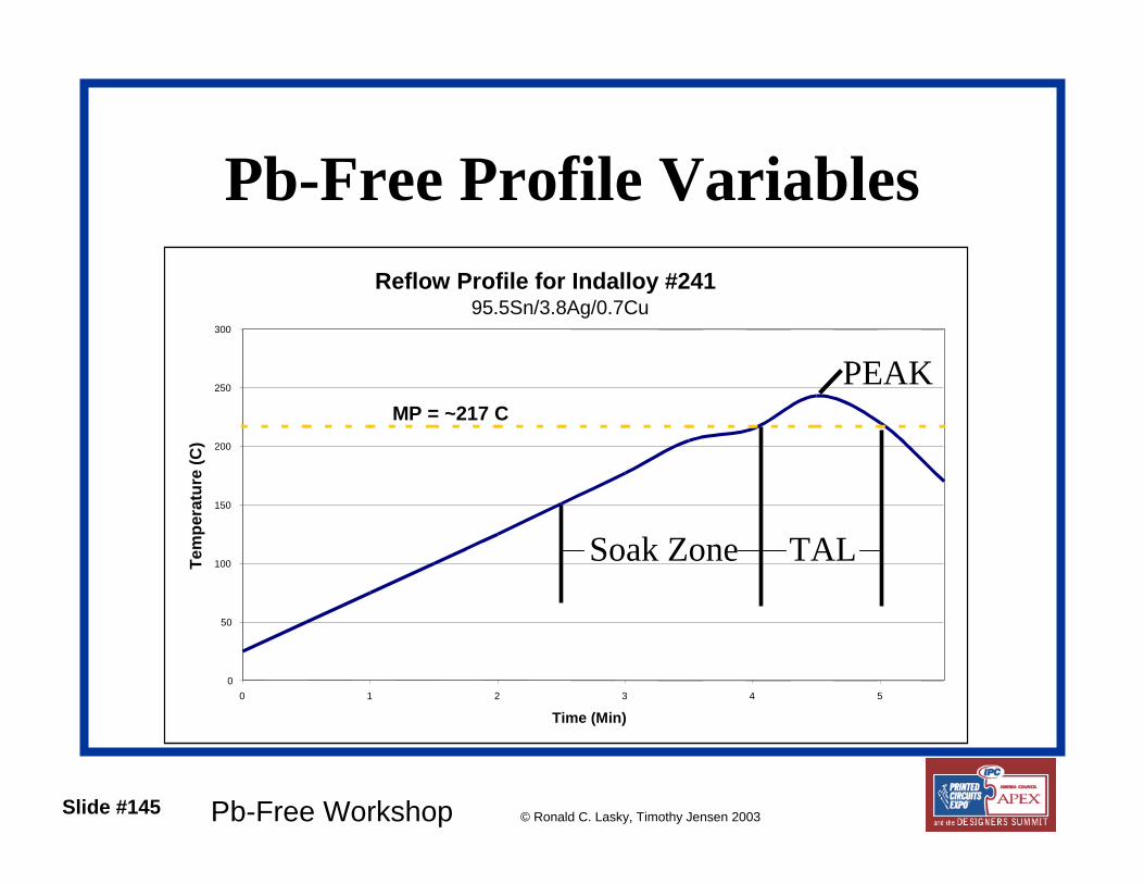
Pb-Free Profile VariablesReflow Profile for Indalloy #241
95.5Sn/3.8Ag/0.7Cu
0
50
100
150
200
250
300
0 1 2 3 4 5
Time (Min)
Tem
pera
ture
(C)
MP = ~217 C
Reflow Profile for Indalloy #24195.5Sn/3.8Ag/0.7Cu
0
50
100
150
200
250
300
0 1 2 3 4 5
Time (Min)
Tem
pera
ture
(C)
MP = ~217 C
Soak Zone TAL
PEAK
Slide #146 Pb-Free Workshop © Ronald C. Lasky, Timothy Jensen 2003
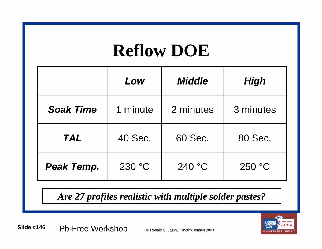
Reflow DOE
250 °C240 °C230 °CPeak Temp.
80 Sec.60 Sec.40 Sec.TAL
3 minutes2 minutes1 minuteSoak Time
HighMiddleLow
Are 27 profiles realistic with multiple solder pastes?

Slide #147 Pb-Free Workshop © Ronald C. Lasky, Timothy Jensen 2003
Categorizing the Response Variables
• Potential defects need to be ranked according to each individual process.– Which is more critical to the process?
• Probe testability• Residue color and quantity• Etc.
– Which is more detrimental to the product?• Voiding• Tombstoning• Bridging• Etc.

Slide #148 Pb-Free Workshop © Ronald C. Lasky, Timothy Jensen 2003
Analyzing the Overall Results
• 60 – 70% of all defects are attributed to the stencil printing process.– Should be considered the most important
for overall process consideration• Reflow is a new crucial variable for
Pb-Free– Not necessarily an issue for paste– Critical for components and boards
Slide #149 Pb-Free Workshop © Ronald C. Lasky, Timothy Jensen 2003
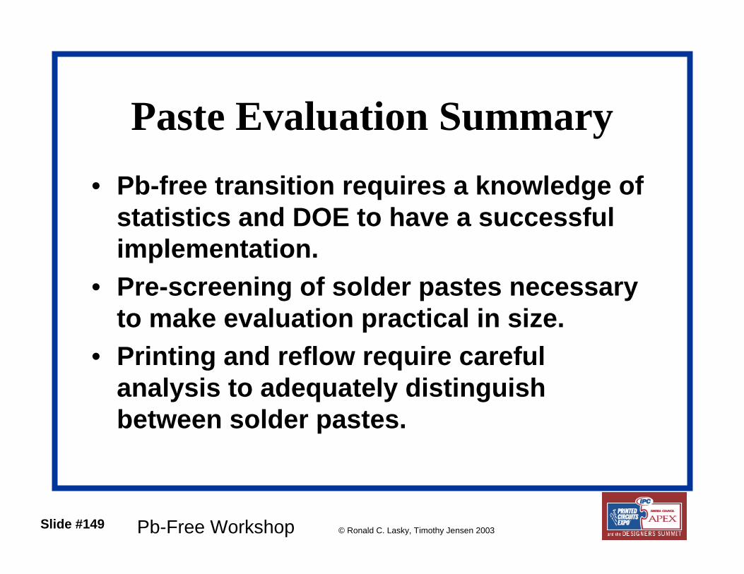
Paste Evaluation Summary• Pb-free transition requires a knowledge of
statistics and DOE to have a successful implementation.
• Pre-screening of solder pastes necessary to make evaluation practical in size.
• Printing and reflow require careful analysis to adequately distinguish between solder pastes.

Pb-Free Workshop © Ronald C. Lasky, Timothy Jensen 2003
Motorola Pb-Free CellphoneAssembly
Courtesy: Vahid Goudarzi, Motorola

Slide #151 Pb-Free Workshop © Ronald C. Lasky, Timothy Jensen 2003
Motorola’s Process Criteria• Paste must have good response to pause,
tack, slump and other printing metrics• The process/paste must show good
coalescence and solder joint quality in a broad reflow process window
• The reliability of the finished product must be as good or better than the standard Pbsolder
• The process must be simple and robust so that it can be transferred to other locations world wide

Slide #152 Pb-Free Workshop © Ronald C. Lasky, Timothy Jensen 2003
Paste Evaluation/Manufacturing Process Development
• Screen Printing Evaluation • Reflow Profile Development • Tackiness Measurement• Surface Insulation Resistance
(SIR) Evaluation

Slide #153 Pb-Free Workshop © Ronald C. Lasky, Timothy Jensen 2003
Lead-free solder paste suppliers & materials
A3B3
A1B1C1
A2B2C2
Phase # 1 Phase # 2 Phase # 3ABC
Paste Suppliers
Flux Vehicles
Paste evaluation & selection strategy:Work with 8 preferred paste suppliers to develop a lead-free solder paste that meets Motorola’s manufacturing quality & product reliability requirements
These studies were completed using Sn/Ag/Cu, Entek finish boards, & air atmosphere
Pb-free Solder Paste Evaluation
The Finalists:

Pb-Free Workshop © Ronald C. Lasky, Timothy Jensen 2003
Optimum Print Speed, Squeegee Pressure, & Snap Off was set per paste supplier recommendation and validated
Stencil Printing Evaluation• Objective: To ensure Pb-free paste
performs consistently as a function of time
• Variables:– Abandon time @ t=0, t=1, & t=4 hours– Solder paste (A1, B1, C1, A2, B2, C2, A3, B3)
• Output:– Volume measurement using laser system– Visually inspect for smearing and selected
apertures for clogs.

Pb-Free Workshop © Ronald C. Lasky, Timothy Jensen 2003
Selected Inspection SitesBased on gage R&R results
RSC
CSR
ABCDEF
1 2 3 4 5 6 7 8 9 10 11 12 13 14 15 16 171 819 2 02122 23 24
1 2 3 4 5 6 7 8 9 10 1112 13 14 15 16 171 81 9 20 21 22 23 24
OSP Finish Test Vehicle for Paste Evaluation

Slide #156 Pb-Free Workshop © Ronald C. Lasky, Timothy Jensen 2003
Pb-free Solder pastes performed well @ abandon time = 0h
Solder Paste Volumetric Measurement or 12 mils SMD pads @ t=0 h
200
300
400
Paste C1 Paste B3 Control All PairsTukey- Kramer
0.05
Vol
ume
Paste C2 Paste A1Paste B1

Slide #157 Pb-Free Workshop © Ronald C. Lasky, Timothy Jensen 2003
Paste C2 failed @ abandon time=1h
100
200
300
400
Paste B1Paste B3 Control All PairsTukey-Kramer
0.05
Vol
ume
Paste C1 Paste C2 Paste A1
Solder Paste Volumetric Measurement for 12 mils SMD pads @ t=1 h

Slide #158 Pb-Free Workshop © Ronald C. Lasky, Timothy Jensen 2003
Reflow Profile Development
• Objective: To determine reflow process window & identify a Pb- free paste which requires MINIMUM peak temp.
• Variables:– Peak temperature– Time above liquidus– Solder Paste (A1, B1, C1, A2, B2, C2, A3, B3)
• Output:– Coalescent performance– Solder joint quality

Slide #159 Pb-Free Workshop © Ronald C. Lasky, Timothy Jensen 2003
Pb-free 2X3 Full Factorial Reflow DOE• Minimize peak temp. to reduce thermal stress on Components• Interaction between peak temp. & time above liquidus
60Sec. 70Sec. 80Sec.
229C
237C
245C
Time Above Liquidus
Peak Tem
perature
Peak temp
Time above liquidus
Ramp rate
Lead-free reflow profile
P1
P2
P3
P7P4
P5
P6
P8
P9
Selected paste MUST perform equally well @ P1 through P9 in air atmosphere
Reflow Profile Matrix

Slide #160 Pb-Free Workshop © Ronald C. Lasky, Timothy Jensen 2003
Inspection criterion:Coalescent performance @ P1,P2, P3, P4, P5, P6, P7, P8 &P9
Poor Coalescent Good CoalescentPoor coalescent is attributed to powder oxidation during reflow
process in air atmosphere
Reflow Profile Development Cont.

Slide #161 Pb-Free Workshop © Ronald C. Lasky, Timothy Jensen 2003
Poor Solder Joint
Insufficient toe fillet
Good Solder Joint
Inspection criterion:Wetting performance @ P1,P2, P3, P4, P5, P6, P7, P8 &P9
Insufficient toe fillet results in field reliability issues
Reflow Profile Development Cont.

Pb-Free Workshop © Ronald C. Lasky, Timothy Jensen 2003
Flux Tackiness Measurement• Objective: To ensure flux provides sufficient
tackiness to hold components in place during manufacturing processes
• Variables:– Paste life @ t=0;t=1h t=2h; t=4h; t=8h – Pb-free solder pastes
• Output:– IPC-TM- 650 Test Procedure: Measure the force
required to Separate a 5mm diameter probe from paste– Shake Test -Automated vision inspection after
placement

Slide #163 Pb-Free Workshop © Ronald C. Lasky, Timothy Jensen 2003
IPC650 Tack Test - Tack test evaluation result
Tack Test
0
0.5
1
1.5
2
2.5
0 1 2 4 8
Time (Hrs)
Tack
(g/m
m2) Indium 51A
Indium 92JIndium 232-99-2Indium SMQ 230
Tack Test
0
0.5
1
1.5
2
2.5
0 1 2 4 8Time (Hrs)
Tack
(g/m
m2)
Control #1Control #2B1B3
Flux Tackiness Measurement Cont.

Slide #164 Pb-Free Workshop © Ronald C. Lasky, Timothy Jensen 2003
1) Populated PCBs after 0, 4, and 8 hours
2) Image components to determine X, Y, and Theta offsets.
3) Place PCBs on XY table of Chip Shooter & shake PCBs for 120 Sec.
4) Image components to determine X, Y, and Theta offsets
5) Determine delta for before & after shake process
0-1
23
0
-3
12
1
1
-1
21
0
10
-1
1
-4 -2 0 2 4 6
caps
switch
tantalum
caps
3.2x1.6
resistor
X-Offset Y-Offset Theta
Component placement offset after 120 second of shaking by chip shooter
Flux Tackiness Measurement Cont. To ensure flux provides sufficient tackiness to hold components in place during assembly process
Slide #165 Pb-Free Workshop © Ronald C. Lasky, Timothy Jensen 2003
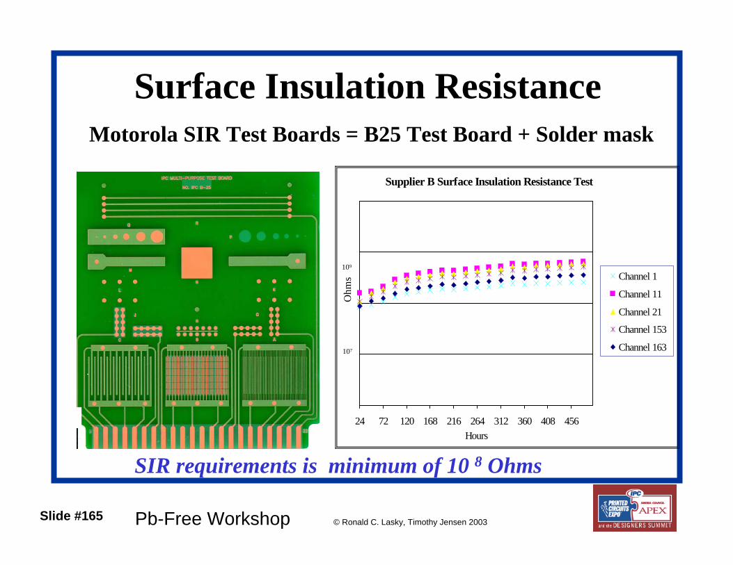
Surface Insulation Resistance
Supplier B Surface Insulation Resistance Test
24 72 120 168 216 264 312 360 408 456Hours
Ohm
s Channel 1
Channel 11
Channel 21
Channel 153
Channel 163107
109
Motorola SIR Test Boards = B25 Test Board + Solder mask
SIR requirements is minimum of 10 8 Ohms

Slide #166 Pb-Free Workshop © Ronald C. Lasky, Timothy Jensen 2003
Printing PasteVisual Inspection
Volumetric data
ReflowP1,P5,P9
P1,P2,P3,P4,P5,P6,P7,P8,&P9
TackinessInstron IPC650
Shake Test
QualitySolder Joint
ALT
SIRJ-STD B25
Motorola
NT
NT
NT NT
NT NTNTNT
NTNT
NTNT
NTNTNT
NT NTNT
NTNT
NTNT
NT NT
Passed Failed NT Not tested
NTNT
NTNT
NTNT
NT
NT
Paste B3 met all requirements
Paste Final Evaluation ResultsPaste
A1PasteC1
Phase 1Paste
A2PasteC2
Phase 2PasteB3
PasteA3
Phase 3Paste
B1Paste
B2

Slide #167 Pb-Free Workshop © Ronald C. Lasky, Timothy Jensen 2003
Solder Coalescent Comparison @ P1, P5, & P9
B3
@
P1
B3
@
P1
B3
@
P5
B3
@
P5
B3
@
P9
B3
@
P1
B3
@
P1
B3
@
P1
B3
@
P1
B3@P1
B3
@
P5
B3@P9P9
B3@
P5
Good Coalescent
Supplier B paste
A1@P 1
A1@P5
A1
P9@
Poor Coalescent
Supplier A Paste
Paste A1 does not fully coalesce and result in grainy joint due to powder oxidation in air atmosphere
Paste Final Evaluation Results Cont.

Slide #168 Pb-Free Workshop © Ronald C. Lasky, Timothy Jensen 2003
No significant difference in solder joint fillet @ P1, P5, & P9 usingB3 solder paste
Lead-free @ P1(229;60)
Lead-free@ P9(245;80) Leaded @ 210 C
Lead-free @ P5(237;70)
Paste Final Evaluation Results Cont. Solder Joint Evaluation @ P1, P5, & P9

Slide #169 Pb-Free Workshop © Ronald C. Lasky, Timothy Jensen 2003
B3@P1
B3@P5
B3@P9
Sn/Pb
Solder Joint Evaluation @ P1, P5, & P9
No significant difference in solder joint fillet @ P1, P5, & P9 usingB3 solder paste
Paste A1
Insufficient toe fillet
Paste Final Evaluation Results Cont.
Slide #170 Pb-Free Workshop © Ronald C. Lasky, Timothy Jensen 2003
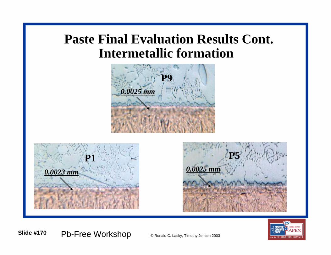
Intermetallic formationPaste Final Evaluation Results Cont.
P1 P5
P9
0.0023 mm 0.0025 mm
0.0025 mm

Slide #171 Pb-Free Workshop © Ronald C. Lasky, Timothy Jensen 2003
Recommened 235C profile
0
50
100
150
200
250
300
0 1 2 3 4 5 6 7 8
Time/min
Tem
p/C
Ramp 0.7 deg/sec
Peak 235CTime above 217C: 70s
Peak Temp. = 235 C +/- 5C; Time Above Liquidus = 70Sec +/ 10Sec
Recommended Profile for B3

Slide #172 Pb-Free Workshop © Ronald C. Lasky, Timothy Jensen 2003
Product Level & Solder Joint Reliability Evaluation
• Drop Test
• Shear Test
• Liquid-to-Liquid Thermal Shock
• ALT for different Products
Reliability Evaluation
Pb free solder joints MUST perform equal or better than leaded solder joints
Slide #173 Pb-Free Workshop © Ronald C. Lasky, Timothy Jensen 2003
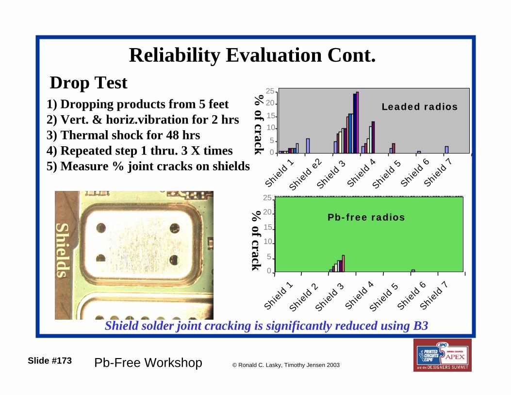
1) Dropping products from 5 feet 2) Vert. & horiz.vibration for 2 hrs3) Thermal shock for 48 hrs4) Repeated step 1 thru. 3 X times 5) Measure % joint cracks on shields
Drop Test
Shield solder joint cracking is significantly reduced using B3
Pb-free radios
Shie
ld 1
Shie
ld 2
Shie
ld 3
Shie
ld 4
Shie
ld 5
Shie
ld 6
Shie
ld 7
0
5
10
15
20
25
% of crack
05
10152025
Shie
ld 1
Shie
ld e
2Sh
ield
3Sh
ield
4Sh
ield
5Sh
ield
6Sh
ield
7
Leaded radios
% of crack
Drop test vehicle
Shields
Reliability Evaluation Cont.

Slide #174 Pb-Free Workshop © Ronald C. Lasky, Timothy Jensen 2003
0.5mm CSP CSP
SOIC
0.5mm Conn.
BGA
0.5mm QFP
0.75mm CSP
0.8mm CSP
20X40 Cap.
DIME
0.5 mm CSP
• 6X6 mm Package size • 0.5 mm pitch partial array • 0.3 mm solder balls size
Solder Joint Reliability Evaluation Test Vehicle
Reliability Evaluation Cont.

Slide #175 Pb-Free Workshop © Ronald C. Lasky, Timothy Jensen 2003
•0
•1
•2
•3
•4
•5
•6
•7
•8
•9
•10
•Ceramic•Inductors
•Tantalum
•Capacitors
•Small
•Capacitors
•Ferrite Bead •Mid-size
•capacitors
•She
ar a
t fai
lure
(kg)
•[afte
r the
rmal
sho
ck]
•SnPb
•SnAgCu
Shear Test
No significant difference in shear force after LLTS.
Reliability Evaluation Cont.

Slide #176 Pb-Free Workshop © Ronald C. Lasky, Timothy Jensen 2003
Variables:- Solder Paste (Paste B3 & Pb Paste)- Component Type ( 0402, 0603, 0805, BGAs, CSPs, VCO,
Transformer)
Output:- Electrical test at every 75 cycles for 450 cycles- Red dye analysis at 150, 300, and 450 cycles
Liquid-to-Liquid thermal shock evaluation (-55 °C to +125 °C)
Reliability Evaluation Cont.

Slide #177 Pb-Free Workshop © Ronald C. Lasky, Timothy Jensen 2003
Failed Joint
Passed Joint
Failed Joint
Red dye evaluation result
No significant difference in cracked area in leaded and Pb-free joints
Cra
ck a
rea,
%
-25
0
25
50
75
100
125
Pb-free Sn-Pb
Solder
All PairsTukey-Kramer 0.05
Joint crack data for different components
Liquid-to-Liquid thermal shock results after 450 cycles
Reliability Evaluation Cont.

Slide #178 Pb-Free Workshop © Ronald C. Lasky, Timothy Jensen 2003
Products Built with Pb-free Paste
* i1000 iDEN
* Concorde iDEN
* i1000 Charger
* i700 iDEN
* i85 iDEN
Products built with Pb-free solder paste and passed ALT

Slide #179 Pb-Free Workshop © Ronald C. Lasky, Timothy Jensen 2003
Manufacturing Issues• Tombstone Failures
• Air Voids on CSPs
• Logistics: Have a Plan to Avoid mixing SnPb and Pb-free Assembly

Slide #180 Pb-Free Workshop © Ronald C. Lasky, Timothy Jensen 2003
20X40 Tombstone FailuresLead-free Solder paste is more prone to tombstone failures due to higher coalescent force.
T1 T2T3 T3T4
T5
Before Reflow After Reflow
T1 & T2 : Tack ForceT3 : WeightT4 : Surface Tension (outside)T5 : Surface Tension (underneath)
T4 is significantly higher using lead-free solder paste
Manufacturing Issues Cont.

Slide #181 Pb-Free Workshop © Ronald C. Lasky, Timothy Jensen 2003
Blind Via
Tombstone failures are attributed to lead-free solder paste & blind vias
20X40 Tombstone Failures
Pads without blind vias did NOT show tombstone failures
Manufacturing Issues Cont.

Slide #182 Pb-Free Workshop © Ronald C. Lasky, Timothy Jensen 2003
20X40 Pad Design for Conventional PCB
Stencil design to minimize tombstone failures on pads with blind vias
.047"
.015" .018"
C .022"
.007"
.008"
.011"
0402 Stencil Aperture Openings
A*.041"
Evaluated Circle, ½ Circle, Rectangular (vertical & horizontal),Oblong, square stencil, etc.
Manufacturing Issues Cont.

Slide #183 Pb-Free Workshop © Ronald C. Lasky, Timothy Jensen 2003
Tombstone / floating Failures
Paste volume was reduced to eliminate tombstone failures on large discrete inductors
Manufacturing Issues Cont.

Slide #184 Pb-Free Workshop © Ronald C. Lasky, Timothy Jensen 2003
• 6X6 mm Package size • 0.5 mm pitch partial array • 0.3 mm solder balls size
Voids
DIME
0.5 mm CSP
Air voids on CSPsManufacturing Issues Cont.
Slide #185 Pb-Free Workshop © Ronald C. Lasky, Timothy Jensen 2003
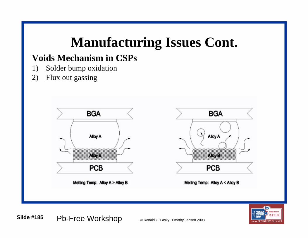
Voids Mechanism in CSPs1) Solder bump oxidation 2) Flux out gassing
Manufacturing Issues Cont.

Slide #186 Pb-Free Workshop © Ronald C. Lasky, Timothy Jensen 2003
Air voids on CSPsBGA/CSPs are more prone to voids mainly due to leaded bumps on package & increased oxidation of powder due to higher reflow temp.
Variables:- Ramp Rate- Solder Paste
Outputs:- Number of voids- Void size
Paste B3
Solder Pastes
Ram
p Rate (D
eg./Sec.)
0.5
0.8
1.5
Paste #15 Paste #16
CSPs CSPs CSPs
CSPs CSPs CSPs
CSPs CSPs CSPs
Manufacturing Issues Cont.

Slide #187 Pb-Free Workshop © Ronald C. Lasky, Timothy Jensen 2003
Void Quantity VS. Ramp Rate
• Quantity of voids are not significantly affected by ramp rate• B3 shows significant reduction in void size as ramp rate increases
Air Voids in CSPs joints
5
10
15
20
25
0.5 Deg/sec 0.8 Deg/sec 1.5 Deg/sec
_ID_
All PairsTukey-Kramer
0.05
10
15
20
25
30
0.5 Deg/Sec 0.8 Deg/Sec 1.5 Deg/Sec
Ramp Rate
All PairsTukey-Kramer 0.05
Average V
oid Size (% of joint)
Manufacturing Issues Cont.
Void Size VS. Ramp Rate

Slide #188 Pb-Free Workshop © Ronald C. Lasky, Timothy Jensen 2003
Coalescent Performance Comparison
Pb-free Paste has a significantly higher Coalescent force
Pb-free Joint&Component Appearance4) Joint & Component Appearance
Pb Before Reflow
Pb Paste Before Reflow
Pb paste printed onto Cu coupon
Pb free Paste Before Reflow
Pb free paste printed onto Cu coupon
Pb Paste After Reflow
Pb paste fused onto Cu coupon Pb free paste fused onto Cu coupon
Pb free Paste After Reflow

Slide #189 Pb-Free Workshop © Ronald C. Lasky, Timothy Jensen 2003
PasteB3 Control(Pb)
Solder Joint Comparison

Slide #190 Pb-Free Workshop © Ronald C. Lasky, Timothy Jensen 2003
Shield Discoloration
Leaded reflow profile Lead-free reflow profile
SnO & SnO2 is formed after lead-free reflow process.
Oxidation does not affect electrical performance
Pb-free Joint &Component Appearance Cont.

Slide #191 Pb-Free Workshop © Ronald C. Lasky, Timothy Jensen 2003
Solder Paste Selection - Evaluated 19 different Pb-free solder pastes and selected B3 based on manufacturing and product level reliability requirements.
Manufacturing processes - Reflow profile, screen printing operation, tackiness evaluation, etc. completed
Reliability Evaluation - Pb-free solder joint reliability evaluation has shown equal or better performance compared to current materials
Components - 100% of the components Pb-free qualified
Electrical & Mechanical - 100% completed with NO issues
Quality - No manufacturing/product quality issues; DPHU goal were met
Motorola Pb-Free Implementation Summary

Slide #192 Pb-Free Workshop © Ronald C. Lasky, Timothy Jensen 2003
Motorola Pb-Free Summary
•Production since 09/04/01
•Many site implementation
•More than 1M cell phones have been shipped to the field
• No field reliability issues have been encountered

Pb-Free Workshop © Ronald C. Lasky, Timothy Jensen 2003
Wave Soldering and Large Board Issues

Slide #194 Pb-Free Workshop © Ronald C. Lasky, Timothy Jensen 2003
Lead-free Complex Board• Functional units were assembled using current materials,
equipment set and a no clean Pb-free solder paste
Pb-free thermal profile• linear heating ramp – 0.9 °C/s• average peak temperature - 247
°C• dwell time – 75s above 217 °C• Courtesy: Eddie Hernandez, HP
mid-range server board • materials
– surface finish: Ni/Au– board resin: hi Tg FR-4 resin– current component
technologies

Slide #195 Pb-Free Workshop © Ronald C. Lasky, Timothy Jensen 2003
Large Board Summary• Higher delta T on board => higher
peak T = 245oC– Reflow profiling and control much more
important• DOE needed for Process
Optimization• NiAu and OSP were successful• Similar manufacturing issues to
Motorola

Slide #196 Pb-Free Workshop © Ronald C. Lasky, Timothy Jensen 2003
Wave Soldering
• Must use SAC, not SnCu– SnCu does not process well and can cause
Tin Pest• Process Control is crucial

Slide #197 Pb-Free Workshop © Ronald C. Lasky, Timothy Jensen 2003
Transformation of Beta-Tin into Alpha-Tin in Sn-0.5Cu at T <10oC
Ref: Y. Karlya, C. Gagg, and W.J. Plumbridge, “Tin pest in lead free solders”, Soldering and Surface Mount Technology, 13/1 [2000] 39-40

Pb-Free Workshop © Ronald C. Lasky, Timothy Jensen 2003
Wave Soldering Overview
Fluxer
Preheating (IR) Preheating (IR) Exhaust
Laminar WaveChip Wave
Conveyor
Air KnifePreheating (CVX) Preheating (CVX)
CoolingFan
Inspired by Steve Breed, Speedline

Slide #199 Pb-Free Workshop © Ronald C. Lasky, Timothy Jensen 2003
The Process• Angle of Conveyor:
Typically fixed at 6o
• Conveyor Speed: – Thermal Mass Dependent – 150 cm/min typical
• Flux: According to Specs!• Preheat parameters:
– Too hot =>drives off flux– Too cool => no activation– Temp Rqmts depends on flux
type
• Wave Form– Don’t use chip wave if you
don’t have chips!
• Depth of Immersion: 50%• Solder Purity: Monitor
Monthly• Solder Temperature:
260oC
Slide #200 Pb-Free Workshop © Ronald C. Lasky, Timothy Jensen 2003
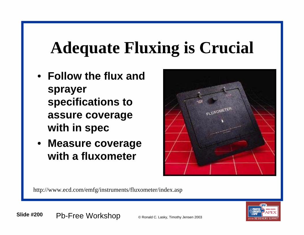
Adequate Fluxing is Crucial• Follow the flux and
sprayer specifications to assure coverage with in spec
• Measure coverage with a fluxometer
http://www.ecd.com/emfg/instruments/fluxometer/index.asp

Slide #201 Pb-Free Workshop © Ronald C. Lasky, Timothy Jensen 2003
Time
Tem
pera
ture
183
C
Board Bottom
Board Top
WaveEntrance of Wave:>100oC Alcohol Flux>120oC Water Flux
“KIC”: PWB Temp Profile
∆T<140oC
Ramp Rate: 2-4oC/s

Slide #202 Pb-Free Workshop © Ronald C. Lasky, Timothy Jensen 2003
WaveCoach™ can Help
Time (sec) 0 90 150 170 200 Conveyour Speed (m/min)Temp Top -C 30 70 90 Length of Waves (cm)Temp Bottom 120 235 160
Time in Wave (s) 3.86 PWB Bottom ∆T 115.00 Cool Down Rate (C/s) 2.50 PWB Bottom T at Wave 120.00 PWB Top T at WaveWithin Spec? FALSE FALSE TRUE TRUE
Results
Time
Tem
pera
ture
183
C
Board Bottom
Board Top

Slide #203 Pb-Free Workshop © Ronald C. Lasky, Timothy Jensen 2003
The Contour Wave FormPWB pulls solder over exit
Courtesy: Electrovert

Slide #204 Pb-Free Workshop © Ronald C. Lasky, Timothy Jensen 2003
Calculating:The Dwell Time
• Dwell time (DT) related to conveyor speed (CS) and “length” of wave (LW).– DT = LW/CS
• LW = 3 “, CS= 5’/min– What is DT?
• Use LevCheck™– Glass with grid

Slide #205 Pb-Free Workshop © Ronald C. Lasky, Timothy Jensen 2003
Optimizing the Process1. Setup the Fluxer2. Establish pre-heat
profile3. Set the contour
wave to just pull solder over the exit wing• Only use chip wave
if you have chips
4. Set depth of immersion at 50%
5. Monitor solder purity monthly• Alpha “Pot Rite”
program6. Set Solder
Temperature7. Set Dwell Time

Pb-Free Workshop © Ronald C. Lasky, Timothy Jensen 2003
Thanks for Coming!