Embed Size (px)
Citation preview
Best Available OCk'ý)
AD-A019 098
TEST PROCEDIURES FOR EVALUATING TERMINAL PROfECTJOfl-DEV'ICE~S tUStD'jN 041P APPLICATIONS,
Robert 't.' Will iams, Jr.
Harry Diamond Laboratories,
Prepared for:
Defense'Nuclear Agency
June 1975
DISTRIBUTEDBY
UI. Si SEPARTUE OF CUMMOCE
ýNl
al
Ir,
-,J6
'40 -1JNI
;d6'
AW. V IS%'-

Best Available CopyS I C U RI T Y C L A S S I VI C A T s O 6 O f T a t S P A U E M e * h)m a I rI I c
REPORM DOCUMEMTATION PAGE uFOI co PLZMGFOM. MU2 i. SOOY ACCISMIO M, 1. IMMIISM? CATALOG MUM9O0
IIDL-TR- 1709
6. TITLE m'•m ,,W4 J S TV19 of REPORT 6 PemoocovM01OTest Procedures for Evaluatinq 'rI:,r ,] .
Protection Devices Used in EMP Applic- Technnical Report.OnS r. Penowm Nio Oki. MlEPOT MUmSIM ..
I. AUTiDT4O 6. CONThACI O311 GRAM9 ' ou"Saw
Robert L. Williams, Jr.
f. PgINPONM4MOOIQGAIZATIOtWAVE £"a ADOIISIS t*PT.TS
Harry Diamond Laboratories Pro;. Ele. 6.27.04.112800 Powder trill RoadAdelphi, MD 207d3 _
ti. CO TRO1. o4110 O V ilCC "WE "aO LOGRA It. 'IPORT O ,Tk-Director June 1975Defense Nuclear Agency to. nuo"M OF PAou
Washington, DC 20305 _
14. MO RI rM* AENwCy NAMAE a ALUDIFIO, I 01=# -CM M an 01090) 15. SECUNITY CLAr. (at we poip )
Unclassi tied
"S 5 "jtTQ Ii TEEI I III Ran
Approved for public release; distribution unlimited.
M? DISTRIBUTION ITATivesir (.15oh aba~e -aAE to sitee so. it eithnitsin nw#
,S uPCPOI.ONARNOT HDL Proj. No. E044E2 AMCMS Code-69I000.22.10922
This work was completed in July 1974.This research was sponsored by the Defense Nuclear Agency underSubtask R99QAXEB099, Work Unit 41, Circuit Protection andHardened Networks.
W. Kay gSoilt (Gumbsus 4 moamaa aA to .aftvn d daaUMV Ms.h mawbei)
Terminal protectorsElectromagnetic suppression devices
0. AtTRACT (Me= ZMwre alg ilto -. *so" MW khflt 6Feaka 4MmiiCertain commercially available components have, been tested to
establish test procedures for characterizing torminal protectiondevices used in electromagnetic-pulse (EMP) applications. Thedevices tested include spark gaps, filters, avalanche dicdes, andvarious other nonlinear components. Square pulses of 50- and500-nsec duration and up to 11 kV in amplitude, with rise times of2 to 4 nsec, were applied to the devices. Response time and enerqyleakage were recorded for each test. Inseetion loss and approxi-
OD j, 1• 43 lornaoN o, I NOV so of oM.OLIT9 1',:( *.!ASS I F IM)
SECURMTY CLAGNICATIGU or ToIS PLO•o hm Dille
IIII III I I i ,,, . ... + ....... . . .

$a[I VUN • • CL. ASEIrc A TIsO0 OF VmS PAGlE~ ~ '4.. t'.d
mate gailure level were measured fcr each device. ResultR arepresented in tabu.l.ar for.7. The devices that appear suitablefor teeminal protection ifncludu spark gaps, some filters, andsome semiconductor devices with bzeakdown voltage less than
50.
I
.I
St(.'jrr.AS~ m Ti-'r T'. "I ~ ~~~~~SECufIt'¶ CL* SSIUSC*TIONl O~r 7045• AJ/.•I 1'm...4g.. I~l
tI
K-

UZ
w-rc--~~~-Ir ---- WAla tr r Ksams
-4:4
Bes Avaiabl Copy~

RIAC:I
Thi• work was sponsored by the Defensie -u4clear Agency undersubtask R99(AXEl099, TheoreticAl and Lx-perimentid EMP. Hardening.Several HDL staff members have contributed toward this proqram. Initialplanning of the test sequences wds carried out by Herbert S. -McBride(formerly of HDL). The . devices were acquired anr tested byWilliam C. Gray. George Uornak. directed the overall procjrdm..
mI-
!A

I
1. INTR, )DU'ThI)N .............. ......................... . '.
• i. I~ : .-ta t vmk,rý r f '.,, . .m . . .. . ..7
I.: Ob i c,.' C vt•; I Ve
.. .S.'t Th .f D..i. .. . . . . . . .. .
. TEST PROCEDURE . . . . . . . . . . . . . . . . . . .. ". .... . .
I. INSTRUV P:NTATION . . . . .. . .. .. . . . .. ... . . ..
3.1 Pulsers . . . . . . . . . . . . . . . . . . . . . . . . .
3.2 Measuremont qectinn . II
3.3 Oq jillo,;',i;es aid Caimcra ;. ................. . .. .
3.4 Curve Tracer ............................................. 1.2
3.5 Spectrum Anal'yzcr ............. .................... ... 13
4. RF.SULTS ......................... ....................... 13
4.1 Important Cbs.4rvabh:... . ...... ................... 13.
4.1.1 Ine,-timn L ...... ..•. .................. 1.
4.1.2 Survivability, ................. .................. 14
4.1. 3 ,: , cn:;: Tin m,, .*d .v, r:.hcot . ................... . 7
4.1.4 Clamp Level ... ............... ... 43
4.2 1',erivable 4,'uantities . . . . . . . . . . . . . . . . . . 4!
4.3 Discussion of Devices ......... .................. ... 43
4.3.1 Sp.ark Gaps. . ................... 41
4.3.2 Filters ............. ..................... .. 4..
4.3.3 Avalinche Diod,,s ......... ................. ..
4.3.4 Miscellanoous 3emiconductor Dowc-....... ....... 4.
S C"NCLUS IONS . . . . . . . . . . . . . . . . . . . . . . .. . . 4"
A . RECOWMENDATIONS ........... 4R
6.1 I ndividual Devicus . . . . . . . . . . . . . . . . . .. 41
6.2 Combinations of Il.vit, .............. .................. 41
IAPPENDIX A. A.. ;.alycludl Modl for tht: Fa:st Pulsur Used in
Co-m. ,;.; nrnt Testinq ... . . . . . . . . . ... . J.
APPLNDIX B. Calcu.ation of .:nerqy Lt:,akage Thr.ouqh TPD into aMatched Lnad from a Pulsed I•r.*ut .........
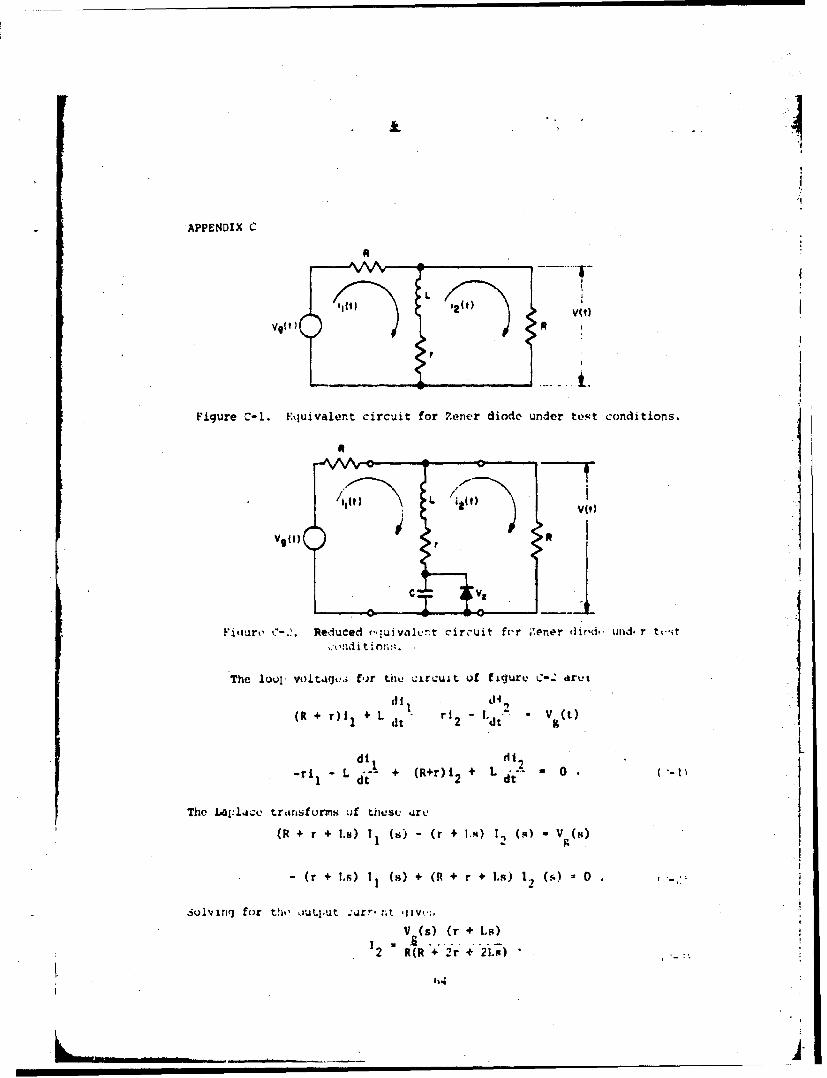
APPENDIX iC. Analysis of Equivalent :ircuit of j WLudt, under Test
Coniditions . . . . . . . . . . . ... . .. . . . . A
APPENDIX D. Thnermial esponse of Semicondut-'r Juznction.s underAppli.•.ation of .. Sequence of Pulses ...... . )
DISTRIBUTION.... . .......... . .......................... ...
• 1 1 1 I I I I I I I I I I I II I I I - " " "-:1
ILLUSTRATIONS
Fi.gure
1 Logic flow chart for pulse testing and evaluation %f
terminal protection devices (TPD) ......... 10
2 Schematic diagram of pul.w generato:s used for testirngof terminal protection devices . .. ...... 11
3 Schematic diagram of measurement sections used in pulsu Itesting the. terminal protection devices,.. ....... 12
4 Schematic diagrain of zuy-ectrwt analyzer t-st ..... .... 13
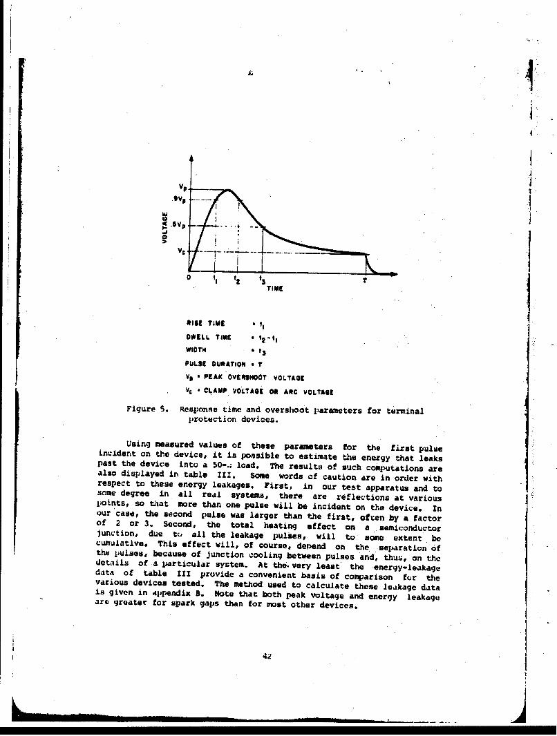
5 Rosponse time and overshtot paramtetrs for terminlzaprotection devices .... ................ 4.
A-I Circuit diagram of pulse-forminq line . ...... . 5.
A-2 Life history of current wave in pulse-foeming lin: , IA-3 Life history nf voltage wave in pulso-forming line . ,
B-i Approximate output voltage waveform for TPD underpulse test conditions ..... ............... . .
C-i Equivajant circuit for Zener diode undr testc'ondit ions . . . . . . . . . . . . . . . . . .. . . •
C-2 Reduced uquivairnt circuit for Zener diode under testconditions ............. ................... t4
D-l Simple, 'ne-dimvrnsionar. thermal model of semiconductordiode ". .
D-2 One-dimensional thermal model of semiconductor diodewith two bulk regions ...... ............... ..
D-3 Threr.-dimen.siondl thermal model uf wt-miconductordiode ........................ .... ....
____ A
TABLES
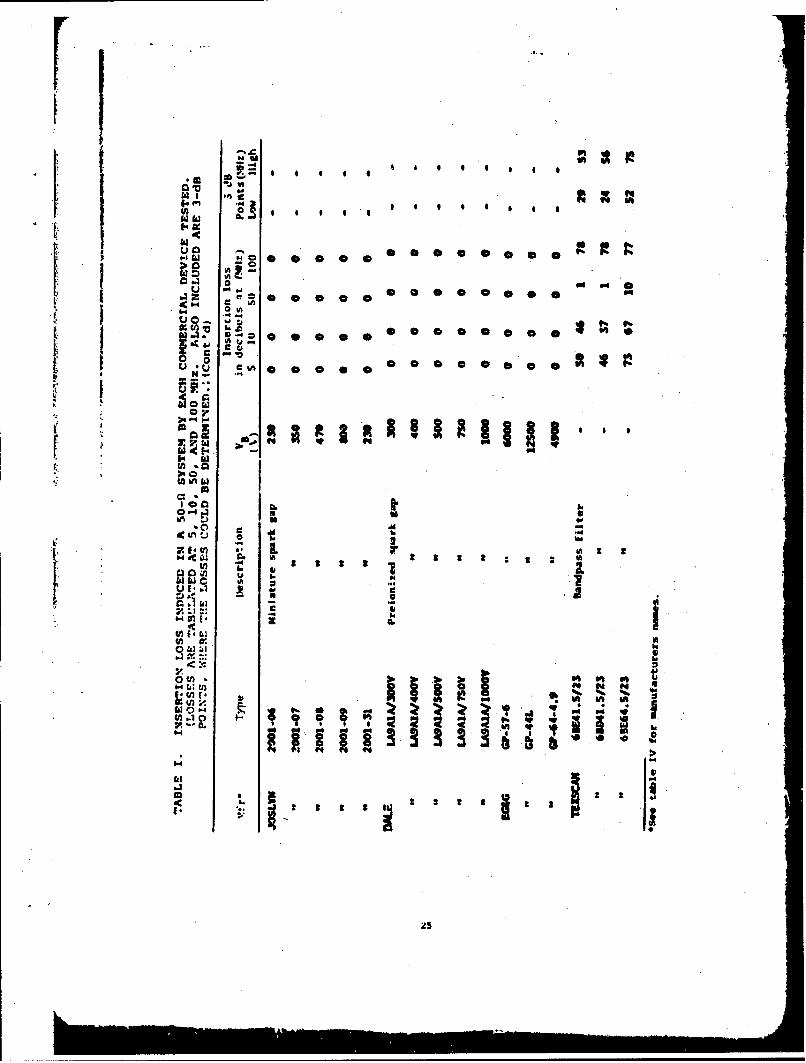
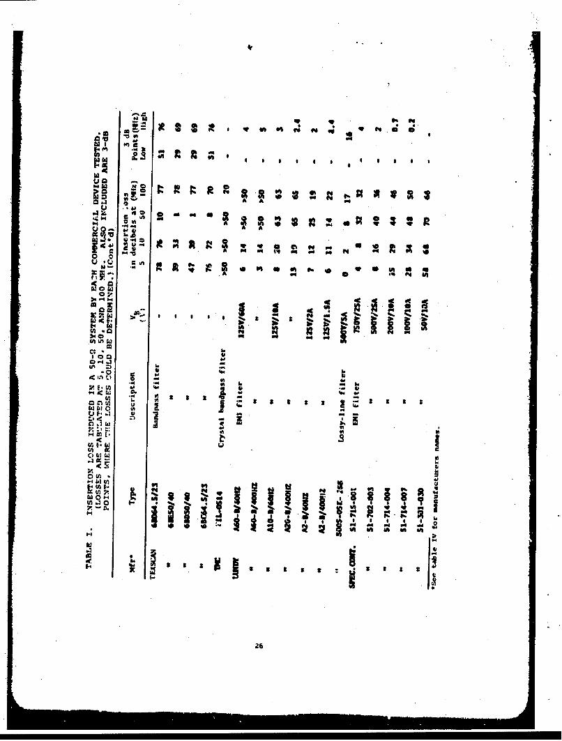
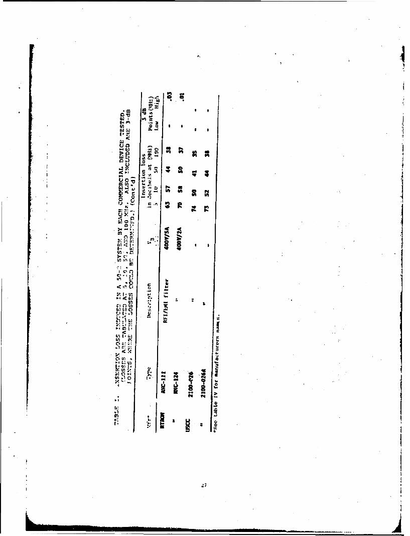
Insertion Loss Induced in a 50-,. System by EachCommuercial Device Tested . .............
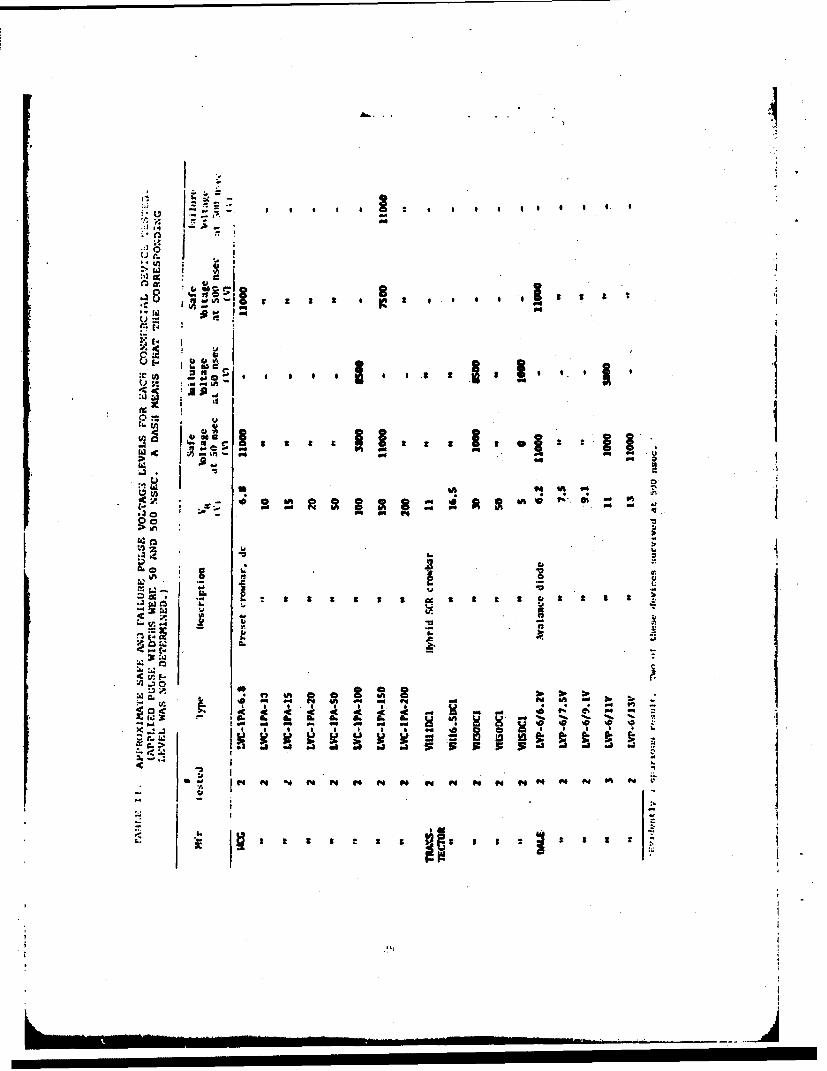
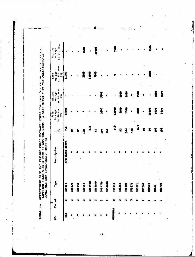
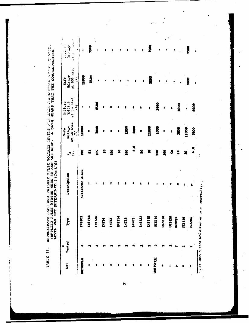
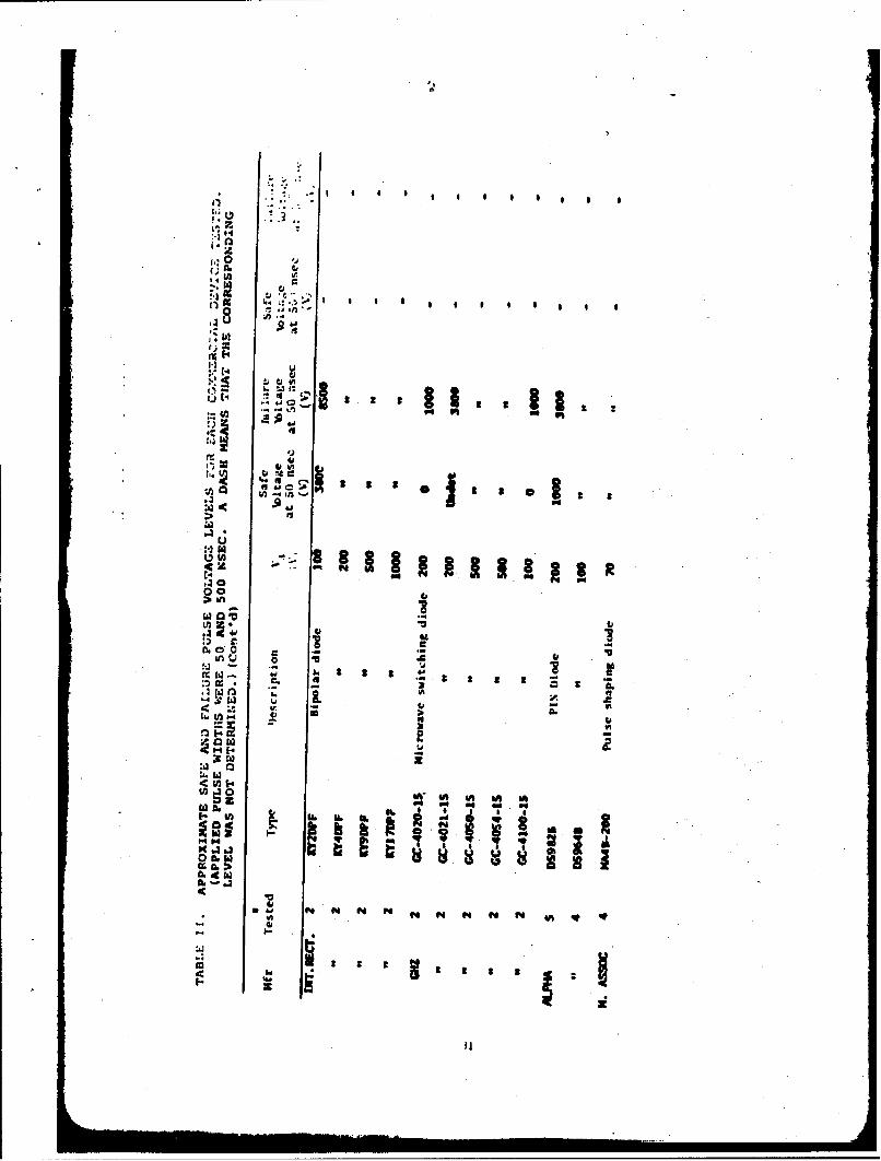
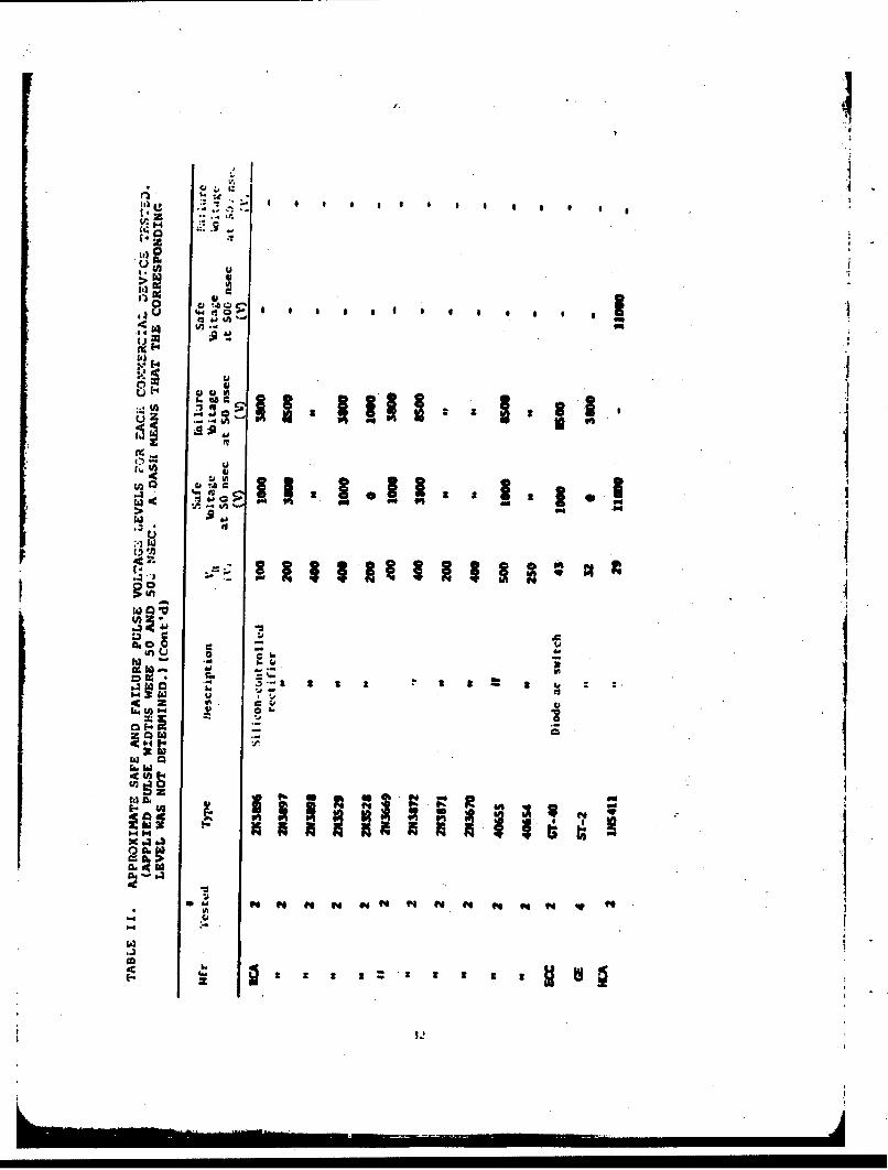
II Approximate Safe and Failure Pulse Voltage Levels for,Each Commercial Device Tested ............
III Voltage Overshoot Parameters for Each ComwercialDevice that Survived all 50-nsac Pulse Tests . . o , 3,s
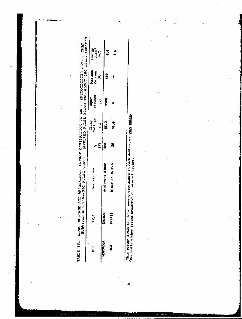
IV Clamp Voltaqe and Approximate Energy Dissipation inEach Semiconductor Device that Survived all 5UO-nsecPulse Tests ....... ..................... ..44
SII

±.I 6t-Atement Luf P'roblit~i,
nuc.Ie~ar weL'dJo:~i LI.J:1kut iaq-.sr- v1 ~'~~:1,1 '.re;' :* wi r:;,S11 nte*ritnan&z contc,:tud to' :e.'n.;itivc xi~ .al.md **t~t.~thereb. causinq motumnt~ary or p'cm-inet d.r.tu;ir. thte opert.tion ofthis~ equip~ment. Whil qcLrouunding and :;!iuauId i ne tec. hniqu*Žs Can1effec~tively divert the* dircet VMP wavtc, thc inT.1,ed uenrqy must be.p~revented from entterinq via thet termin-Als of t.iu viquipimt:nt. Thust- thereis a need for terminal protu':tinn devices; (ITI'I,)', bo~th for retrifittinyexistinq equipmetnt and for use lit the do.-,lqn ..-f new ve1.1uzpment.
The TI'D a~c~td with a qi'Jen termuiil is to be conneftc-Jbetween the -terminrai and qround, thus; roviding it .titernaite. Piath f,.,rthe itlCidentL trainsien~t current and rtfit..tln,w ~;omeŽ, or perhajps moit'i ofthe anorqy jwjy from the j~ ceiu'uij~me::it. The' more imp%.urt.arit
(a) 1re i:OiL'rtiol, '-:;,; ii%,.-urrvJ by.. i..tiv thu TPDZ !ihoajl~ nutbe so large Q~i to interfertt with thv noi-ital oj '. .itin of tie ysamFor pr. IiaL1urI;L);t:., Uji!; M647 lim;t th.~i;- u ic oh.i:; to -1 %b .overthc f2ru.MuLenc7 rvitle of inteor.;*. In Sme2 ':y;tqvYu:;., theiv. V .Aj.1tncould be limnited L.) a few .i- ?tr';
(b) The TD J&uidU beL -.xipaki.e of *&~.b~i a Larjli- Amouurt ofenergy witlhout 1k. ui. diama.J L!,t:1 vk,ý. A\ lit sc.*:tion: philO.'OIhy tha1tAllows the lrotc,*tiv-,e Cltnrnt to. b.: -1X%1+,! L! the p'ro''cu;,. of providin~gLlrott-ction i;; jnav.;ho -Lremi-, bepxrtni for roj;.&Ilcemerntduring tin atta.i.
(.1 11 ;., b.: n.1.4 eI*J '.L-' f-r:pt~.I~g. b.'Iow t:,,Jti.4.ired ptec' :it itk-i .&LX II t.j i I *pL3i*y t. Ln.a: thlat
* .. lf tm t.-' ,u cwitn whiJ, thi,; tr.&n.iition t-ikv-,i pl.. m-tya be . the, resp.onst, timeof tite TPIT. nrn this tr.1:isit x,.n thc. TIT. v I t.-i;4. may tex vvd theprotection level by a ý;btývxvit*:t-ý, ~ 'er:'-..%t--whi,:h shou.13be minlimal. in amouunt aknd tine. Trhe r.j.uiriemetit.. o~f tht- system b..inrjI.rutecto-d will-lar--jel'7 e:;t~bil:01 linit.; for t*.vL ,:veŽrshoot.
(d) After the initial ovor.shoot, tý.%- TP; should limit tht.train~ient voltage to a reasona~bly ;.atul ranqt' near thi-prote,:tion level,more or less indepe-ndent of the 'current Lpan:inq Utr:-Uqh the device.What Qonstitutes a reasaonable voltage ran';u will b.* determined lairgelyby tho requirements of the system buing Ilrottei-td.
Preceding pag blank

o.uantitatively, the dtusired hiar~acteris'tiý:. of terminal protuction
devices can be derived from th. par~umeter.,; of v.ltatleis and rurrentsIinduced in the .antennas, ant~,~ d .bi of: thu system, anid from thepropevrties. of the s.ystem to b#. jprt.te,;ted. Pkisvd onl f ield cand l.tbor4Jtorytestitng3 experiefl..e, some stanidardsi fur rPI)'.; ho&ve been t'.'ntativelyestablished. First, theo TED) Wihuld be able to i;uj4,-rus3 a voltigetransient of ibout 10 kV, which ipiu a miximai short-circuit currentof about 4101 A in i S0-.. sysitem. Second, thev TPU slhould switc:h from thelow-* to the 'Aigh-conduc:tiun state in less tlh.an 5 nse.-- Third, the 'rPDshould be able to mainta.in this high-corductiun state for at least500 nsec.
1.2 Objectiveg
Primirily, the first-pihase objectivus ut '...u tost j:rqyr~anf were. tufl
(a) De.velop exprjau~ILntAl. tuchni jue.; f(-t ha* craVto-,r iz ini Wideval;.6tiny TPUJs that have potentiil un;ufunin.-4 ±it IEMi atiplications;
W~ ulc experimuntal1 da.ta {dat~t bank) on the in.;ertionlo~,Lli, tflICriy abiorbin'j rel.:pun"UPe timnes, and voltage
(.) :~~vesl i:;trUo. th~tloi..; that. uptirize th2UfflteJ~~ ofTPD'j In arvcific: sysitei ap~i...Latitins. Thest..e results, were e!xpected tugenerate otae.r ben~efits~. For exaurijlv, it w,%:; .intic:ipa.teci that sele.tionzriteritt, ;q-eifivat~itins, and tkce:qt-af,:v te:;t:; fo rou's Could be.,erivud frim Chi -datat ba.-.e.
1.3 SVleCtioui of Oevic:uz
Mtany zhar~ac:te:r1t1L*t of Al.*:r..1*:n~..t;itmity.i:*to'mine
the.ir uuitabil it / f:;r termint"i prote.2t i.nh duvit~~, :ah .v:~iitji
chiaracteristics are not known ;,r-..It ie.v~t have not been pubL'h!ahed Li-I L.",tmainufacturers. In many cases, the :-ipc-anlnjcjaki~lity ha:;not been published becaust? it is not ain impo~crtan:t %:,'n!;ideration in thenormial usage of the J4-vt.-.- . The devices tested in this prOjrazn were,selected on the , .-- ,f a tewhnicai-literature suirvey and fromsuggestions of those experienced it- the field.
2. ThST Pk%.ck:DUftE
To evaluate the effects of pulse t.estinq, it is; netcei:sary toc;ompare zettain elecvtric~al pro)perties of va.;-h :Ivvi,:v Lxlf~lre tepulsetest. with the s5une proplertie.; 'mex-iured after t-h't pu1:se' ttw;t. It waIs

decided that measurements of insertion loss and current-voltalecharacteristics would be adequate for this work, Tnerefcre, before hi.jhvaltage pulse testing, each device was examined on a spectrum. analyzevrto measure its insertion loss from 0.01 to 100 MHz, and each device(except spark gaps and filters) was also examined on a curve tracer.
After being pulsed each device was again tested_ on the curve-tracer and/or spectrum analy~er. Comparisons of pre-test-'and post-testdata were then used to assess component degradation. This pr, .- edure wasfollowed for each pulse amplitude.
In the initial round of tests the pulse width was 50 nsec and theamplitudes--measured across a matched 50-1 load with no TPD inplace-were 1, 3.8, 8.2, and 11 kV. When post-pulse tests indicated.hat a device had'been damaged, no further pulses were applied to thatdevice. A listing of the undamaged or surviving devicus wa. completedafter the tests.
In the second series of tests (which was applied to the survivors-)f the first tests), the pulse width was increased to 500 nsec, and theamplitudes were 3.5, 7.5, and .11 kV. These additional tests were, ofcourse, intended solely to study the energ*7 dissip.-tion capacities ofthe devices to a somewhat greater extent. The 3.5-kV, 500-nsec pulsewas chosen to be roughly equivalent to the 1l-kV, 50-nsec pulse as faras semiconductor-device-junction heating is concerned, assuming thatboth pulse widths lie in the range of applicability of th..e Wunch' modelfor semiconductor junction damage due to thermal effects.
The highest test level of 11 kV was chosen because it was themaximum available and because it appeared to be a good practical test.
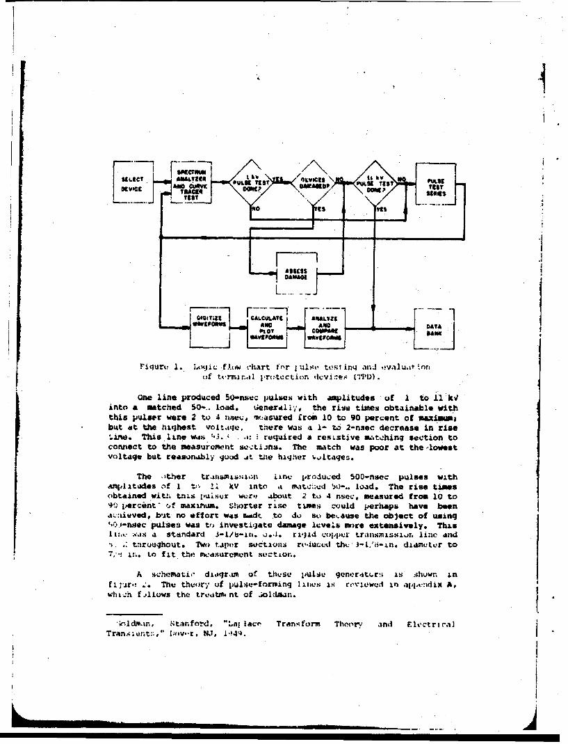
The logic flow diagram for these studies is shown in figure 1.
3. INSTRUMENTATION
3.1 Pulsers
The pulse generators used in these experiments. were of the chargedcoaxial transmission-1-ine type, having two in-line spark gaps to ýreatefast rise times. The gaps were operatcd in a nitrogen atmosphere, andthe pressure dnd gap spacing were varied to give thv fastest practicalrate of rise for each pulse amplitude.
Wunch, D. C., and Bell, R. P., IEEE Tran;. on .%ucl. Sri., Vcl. NS-15,No. 6, Dec lq68.
IL!
TEST
0 a i
ASSESS
CW C"ALCULT AGILIIALVU 1ANDo a-No ago &V
LOtO CoaMPAu .....
Fiqjure. 1. i.oq i fJ. A cwthart :'nr I uls.o tosl inq at-'. ,qV.-Ilua• -. nn
off tur, ral iro:tcCtior, dcvi~ce.ý ('ITD).
one line produced 50-nsec pu.lses with amplitudes of I to 1. k,into a matched 50-.. load. Genralyi., the rise times obtainable viththis pulser were 2 to 4 ulsev, w:asured from 10 to 90 percent of mawt mIbut at the hi;qhest VoLtd(W. there was a 1- to 2-naec decrease in rise
ime. This line was :.:. . required a resLstive miacthinq section toconnect to the measuroemnt sec.LiJns. The match was poor at the lowestvoltage but reasondbly 4ood at t2.e higher ;16taqe5.
The ,it..er tr.anm•*sIn iine produced SOO-nsec pulses witham,lltates of I to:. !, kV intc ,t a 5o-.. load. The rise timesobtained with t.hs 1'uisur were about 2 to 4 nsee, measured from 10 to9' percint- cf maximum. SThorter rise tLoes could perhaps have beentc.:aieved, bi.t no effort was soadr. to do so because the object of using',0.o-naec pulses was to investijate damage 1tvels mr)re extensively. This
was.~ a stiandard~ -/-u .i rij)id coppe.r traIIinsis!ivri line adh), .. � tnruuqhout. Two taptr sections re-,iu~cd the i-L,'i-in. diameter to
7, . 1:.. LO fit. t~h. v•sdsuremwent sM'CtLOr..
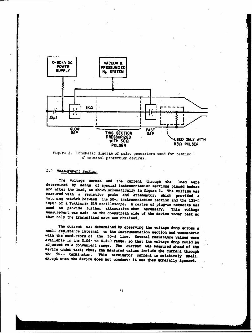
A schemati,- diagqrm of the~se joulse: gener4itri; is .huwn inf ;'Ar.! :. Thu theory of pulse-forming litivs is reviewed in apptedix Aswhih.:h f Alows the treoti. nt of ;oldman.
,.oldd.m, stanford, "La! lacp Tranmform Theory and Flectrrca]l
0-60kV DC VACUUM 1POWER PRESSURIZEDSUPPLY NE SYSTEM
~~ '-I ....
SLOW - " FASTGAP THIS SECTION GAP K
PRESSURIZED 'USED ONLY WITHWITH 50 8S3A PULSEYWTPULSER
Figure 2. Schematic diaqram uf pulsc gen(rators; used for testingof tpr.inal protection devices.
S• 2 Meaaement Soction
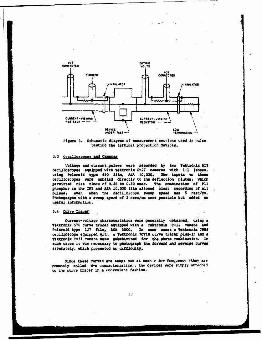
The voltage across and the current through the load weredetermined by means of special instrmentation sections placed beforeand after the load, as shown schematically in figure 3. The voltage wasmeasured with a resistive probe and attenuator, which provided amatching network between the 50-.1 instrumentation section and the 125-flinpur of a Tektronix 519 oscilloscope. A ceries of plug-in networks wasused to provide further dttenuation when necessary. This voltagemeasurement was made on the downstream side of the device under test sothat only the tzansmitted wave was obtained.
The current was determined by observing the voltage drop across asmall resistance internal to the instr•mentation section and concentricwith the conductors of the .50-a line. Several resistance values wereavailable in the 0.04- to 0.4-il range, so. that the voltage drop could beadjusted to a convenient range. The current was measured ahead of -thedevice under test thus, the measured values Include the current thcoughthe 50-1, terminator. This terminator current is relatively mall.ex..ept when the device does not conducti it was then generally ignored.
I,
CONdNECTEDVOT
J.3UREN Ocoikisonc idCmra
Votae ndcurun INULATeR weINeSredULto AeTRoi51
osilosops quppd it TktoixC-? amza wthli lULsusn Plridtpe40fim M 000.Th nItFo hs
p Fittedrie 3.Shmtime iara of 0.e6sto0.m0ent Thec iations use inpulsphosphr in tesCRing the term0 inl alloweindvles. eodigo ~
pul seslloseven ahnd thme oclocp we sedwsSne/
Volraeant-otd charateristics wererecoerdrally tobTaiedruninx a1Tetosiosco urvptree equipped with a Tektronix C-27 cameras aihl lns**Poaridg tPelri ty07 fi10 fims ASA0 0#00 s The- ca puts eto'tes790oscilloscopes equi ppedith airTelytroi tlio delcuretrace plag-in ehdcapetromitte ril cimerao 0.2e sbtitut0ned fo the socombination. ofP1
pulhses, ovt waheneesr toe hoslosraphte forwarped wand reese curesspaooratelywhich asepresent o sc=wrepsil u ded nodifcly
Current-vocltedge- characteristics),wthe deviceslweretainlyausicgeaTetroni t 7e curve tracer inanenuipen wth ashion.xC-2 aar n
Polaroid type 107 fila -ASA 3000,In isecss .ttonx70
* .. -.. o. - .. -. . A
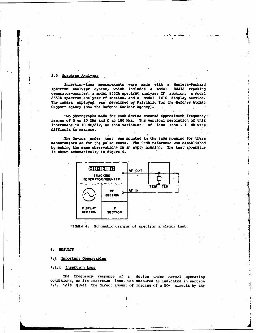
3.5 Spectrum Analyzer
Insertion-loss measurem~ents were made with a Hewlett-Packardspectrum analyzer ysteum, which included a model 8443A trackinggenerator-countera model 8552A spectruv analyzer IF sectiont a model8553A spectrut analyzer rf section, and a model 141S display section.The camera employed was developed by Fairchila for the Defens#' AtomicSupport Agency (now the Defense Puclear Agency).
Two photographs made for each device covered approximate frequencyranges of 0 to 10 MHz and 0 to 100 MHz. The vertical resolution of thisinstrumnt i.s 10 dS/div,,8o that variations of less than -1 db weredifficult to measure.
The device under test -was mounted Ln the same housing for thesemeasurements as for the pulse tests. The O-dB referance was establishedby making the same observationn on an empty houning. The test apparatusin shown schematically in figure 4.
1015111011 191 RF OUT
TRACKING
TEST ITEMR ftPF IN
SECTION
OISPLAY IFSECT ION SECTION
Figure 4. Schematic diagram of spectravn analyzer test.
4.1 arportant Observables
4.1.1 :nsertion Loos
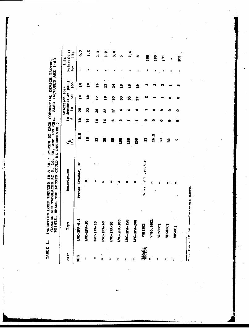
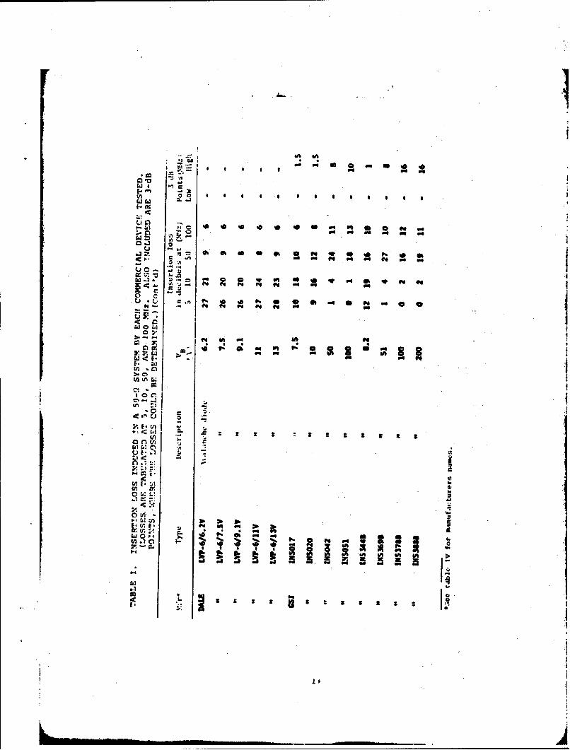
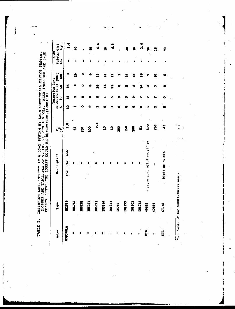
The frequency response of a device under normal operatingcondItions, or its Insertion loss, was measured as indicated in section3.5. This gives the direct amount of loading of a 50-. circuit by the
I'I
_ __l I_.. . .. e iiI . .. . I li - , . .

I.,
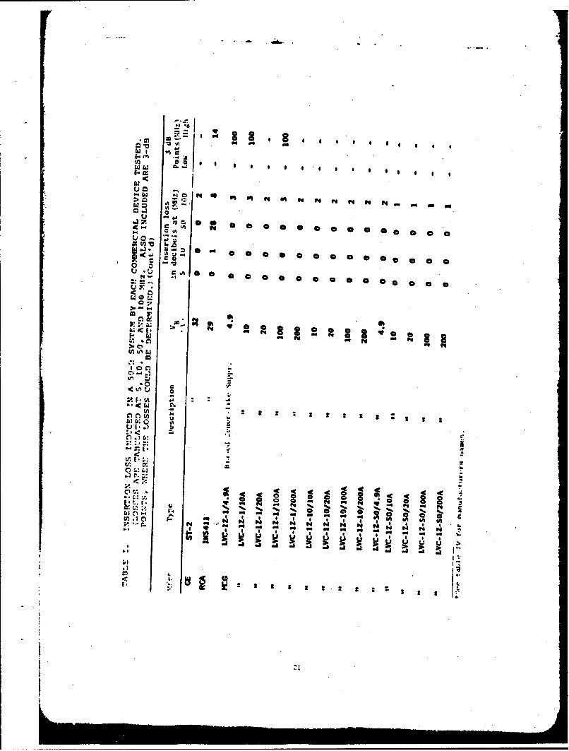
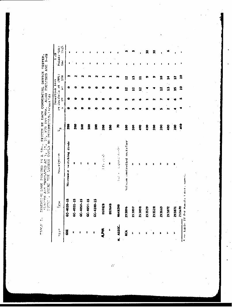
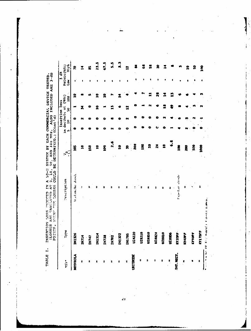
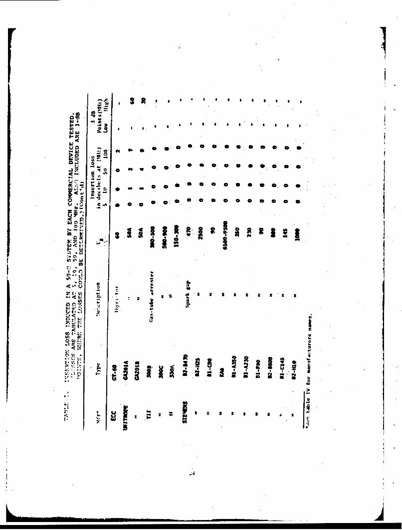
device tn its nonconducting state. It was found that the insertion losscan be well represented by values at a few frequencies. We chose 5, 10,50 and 100 MHz, largely as a matter of convenience, but the choice isnot critical. These results are presented in table I, along with 3-dBpoints (where these could be determined) for all devices tested. Thefrequencies at which the loss passed through 1 dB would perhdps havebeen more useful# but the resolution of the spectrum analyzer was ofsuch that theme points could not.be determined with a reasonableaccuracy. The insertion losses and 3-dS frequencies liSted in table '*are averages over the sample of that particular device type. The sizesof these samples are listed in table II.*
As table I indicates, many semiconductor devices .would be usefulonly at low frequencies because of their high-insertion loss. The moreobvious examples are silicon-controlled rectifiers (SCR's) and someavalanche diodes,. The case of the avalanche diode is particularlyillumirating because the same properties that cause a diode to showhigh-insertion loss-that is, large junction area and small depletionwidth-also allow it to survive larger input transients. The depletionwidth, of course, derives from the impurity concentration, and' a higherlevel of impurity carriers means that more current can be impressedwithout excessive heating of the crystal.
At the other extreme, spark gaps generally exhibit little or no
measurable insertion loss.
4.1.2 Survivability
The approximate level at which a device was- damaged was determinedby comparing pre- and post-pulse curve tracer .and spectrum analyzerphotographs. Damage was defined in this context as any significantditference between the two sets of photographs. This damage wasgenerally evidenced by an increase in leakage current, for example. Inextreme cases, the device either opened or shorted. It turned out thatthe insertion-loss curves were not often useful for damage evaluation,although they did sometimes confirm conclusions based on curve-tracerphotographs. When the device was destroyed, as indicated by the curvetracer, it was occasionally noted that the insertion loss had markedlyincreased; and in rare cases where curve-tracer photographs were notavailable this fact was of some value.
*These tables are included with tabulated data on pp. 13 through 3f.

o .1
INDEX TO TABLES
Table I Tnble II Tables IIi IV
Preset crowbar, dc x x x
Hybrid SCR crowbar x x x
Avalanche diode x x x
Bipolar diode x
Microwave switching diode
PIN DIODE
Pulse shaping diode x
Silicon-controlled rectifier x
Diode ac switch x x x
Biased Zener-like suppressor
Thyristor x
SPARK GAPS
Gas-tube arrester x x
Spark gap x x
Miniature gap x x
Preionized gap X x
FILTERS
Bandpass filte:. x x
Crystal bandpass filter x x
EMI filter x x
RFI/EMI filter x x
Lassy-line filter x xI
l15
U

MANUFACTURERS OF D.'VICES REPORTED IN TABLES.
ALPHA Alpha Industries, IncWoburn, HA
DALE Dale E1Pctronlcs, IncEast Highway 50Yankton, SD 57078
ECC ECC CorporationBox 669Eulesas# TX 76039
1050 EG&G, IncElectronic Products Group35 Congress StreetSalem, MA 01970
GE General ElectricSemiconductor Products Department
alectronics Pk.Syracuse, NY 13201
GRZ GHZ Devices, IncKennedy DriveNorth Chelmsford, MA 01863
GSI General Semiconductor Industries, IncP.O. Box 3077Teqae, AZ 85281
INT. FECT, International RectifierSemiconductor Division233 Kansas StreetEl Segundo, CA 90245
JOSLYN Joslyn Electronic SystemsP.o. Box 817Goleta, CA 93017
UNDY Lundy Electronic & Systems, IncGlen Head, NY 11545
MCeG MC; Electronics279 Skidmore RoadDeer Park, NY 11729
I I I II I i i, , .0

MANUFACTURERS OF DEVIC'ES REPORTED 'IN TABLES. (CONTV')
M. ASSOC. Microwave Associates, IncNorthwest Industridl ParkBurlington, MA 01803
MOTOROLA Motorola SLmiconductor Products5005 E. McDowell RoadPhoenix, AZ 85008
RCA Radio Corlyuration of AmericaRCA solid State DivisionRt, 202Somerville, NJ 08876
RTRON Rtron CorporationP.O. Box 743Skokie, IL 60076
SIEMENS Siemens Corporation186 Wood Avenue SouthIselin, NJ 08830
SPEC. CONT. Slpctrum Control, Inc152 East Main StreetFairview, PA 16415
TEXSCAN Texscan Microwave Products7707 Records StreetIndianapolis, IN 46226
TII Telecommunication-. IndusLrie., Inci37t Akron StreetCoji cguc, L.L., NY 11726
TMC THC System!; (Ariz), Inc930 Wtest 23rd SLr,'et
TRANSTECTOR Transttdtor Syttems532 Monterey Pass Rodd, FV.. Box b10Monterey Park, CA 91154
UNITRODE Unitrode CorIporatio2I580 Pleatsant StreeLWatertown, HA 02711
USCC U.S. Capiacitor C•orporaition2151 N. Lincoln Stre.etBurbank, CA 914504
* 1
'0,
41*04 L
w ooM.- C; ad
ft &M ftq ew 0
22~ d. - 1 6 t 0 6 d 0'
oa;a4 .13 ll
W I~
f- - C - U
ue 0
94aii 0 0 0 U -
-Zt f
0 U
o c -
L.
i P
*r I
h t S
f t
~ ft Ufft
c~o ~ ~ ~.~ O ~ S t f ft 6AiAJ am-
g.~ o
Ac 4
M. v
gaj
w 4
C21
uc41 0 a: 1 * ~i * U s
in f" ft f f t t fV " i
>. -leua LM :a f1 S a q' q
N. -. N
f x t t t
00
(JO - ,
0 o
C ft ~000 . 0 S 0 0
S 0
01
Lm
CAf t t
*0 clC
rE
tncLii...)
AL
(~3 .1.I1
m f A'
IA in * GA r4 0 v
.I ~0 0 CS or50 ~ f 4 t ~ G
-Ic
C.~ L' 0 0 5 A A ' A f
inl 0 0 0 Os 5 m VA0 U t
~.. C'
~-;.x z z s
U~ a.'*..ea
r•.i,. "". 1<
ji
uO -J P 0
4,e r A
54dc z
CJ 7
tn :1
m
"0I..@5 -
CAI~r, ,*:0 - .--
€3• -
0-4 '.1 1;,V. -, r-• a
210
I I. I I I I I . . . .i I S.-
U)
0az 0 0 0 *k *
a 0
cl~.I-' ! *Ew .e . . . . S
411
AS
00 [i 4
see.....w~v
ot
. . * * *I0 0 0 0 *
-' 0 00 0 0
or 04-0
c 0 0 0 0 0
01
Poo ~ * * e . @ o
I C; 9
14 Iii
464
uU I.
CAb
C6 An se
1w 61141
dca
oln *e~~W5
144bii
MM
&C 04 0 IwoS~ S
tiN-
C. .msa V
QZ
IJCA ELA -
NA W. ~ JyI w . aS&C) [Al - q .
1z~b
04
in o .0
6-4 .3 be
4 A
-o ~ 4'Ieee 26
u~. 0 6J
C.. .
4.'
In 00 S
f4 64
w~ 0
ift
.11
0 C .: tý2
cn o~ o~ .
*0 I.
14 2
ri In
IAI-:4 'I
* .3 U
x so in
ft m
[ . I .. ,i.
;a!, ,I I!
4. •'c It O
U 4
@,3 .•.".• '
(A
.4~ LA 3 33
S° I S IS I | I! I3I 3 3
sd, Aj ,,•,It
ab so
it 4.I itf
c U3f
I•., - - U f
Fj o
- • ' ' .' .
iI= .,
I-' "C'
N4- 4 of
'IOA
3.3 3 3 3 3 3 1 ~ 3 3 3 39
44 C-
A
to a E
1-4
taa
w vP44
04
dc V
ot. p4
I0OA c
t 4 Ir. * * * 0
0
V4
tj1:
140
w in
mo U .04, '
.4 I. &
-c IF. Vmw 0-.4
:A. 4,V
W~~# LR U ot f Iftta A$
Fo~ Lo 96 1
WXI ~ D? Sv
tj - .. J
dcdcN N N N N N t N I* Il4
a. W h- 3 3 fA
4p=
Sdi
I Sg -. r
rii
"1. to as I-•' • €• Q I II II I * S I S. I II
u~.•'qIl il4 4m
Jg~ t:
ti
U)UINCI
In U
gau
""- -I !
In . , . 3 3 -
,-~4 .Wb... - I --
ml 94IIII
X
'92~ - i Il l
!ii i a, r4
to.
26
a" p4 ftf...... _p.Ap. p. p. qI p
IA4
z 952
InI
a63 S S S S S 5
4404r
MAjO .-
.
SL 2 8
r4toV
. g a . e S s 9 g *~~vi~i 4,:
114
!3 -
r~IL
go
IA
w 4k
4~4W
th 4 ft f 4 4 Of
9,93
34

It4 I I gI,))
1 4
oo W.A)~L4 1 4
-
i4 U .
g14Ow
96 IA 4 6 4
14 j 4 I 0
*9 -
JJ

1:2 0
44
tn.. -
1-4
fA. 4,
64._0 6) Z 2 : : g
L~6j -i.u

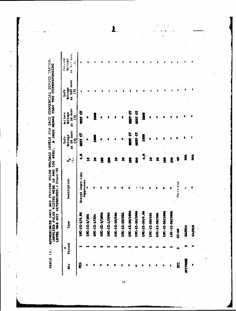
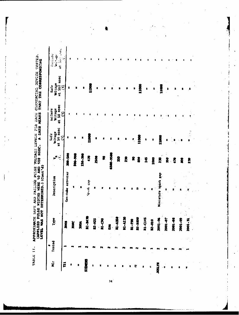
The damage data are summarized in table II. Each device islabelled with the highest value of input voltage for which no devia'e inthat sample sustained damage--this is called the Safe Voltage; thelowest value of input voltage for which any device in that samplesustained damage is called the Failure Voltage. It should be clear thatthese numbers represent no assurance of performance.
in rare cases the existing data did not permit such an evaluationfor a particular device. Some of these cases are labelled with "UNDET"in the appropriate column. In a fes, other cases the devices weredestroyed during curve tracer tests. Tiese are indicated by "DEST CT"
* in the appropriate column, even though other devices in that sample may* have escaped damage until pulsed. F( r damage evaluation, all such
devices were simply considered as untested.
The devices that survived the 11-kV, 50-nsec pulse test includeall spark gaps tested, some avalanche diodes, some crowbars, and some
• filters. Table II shows that the majority of the survivors of thell-kV, 50-nsec pulse test also survived the It-kV, 500-nsec pulse test.
4.1.3 Response Time and overshoot
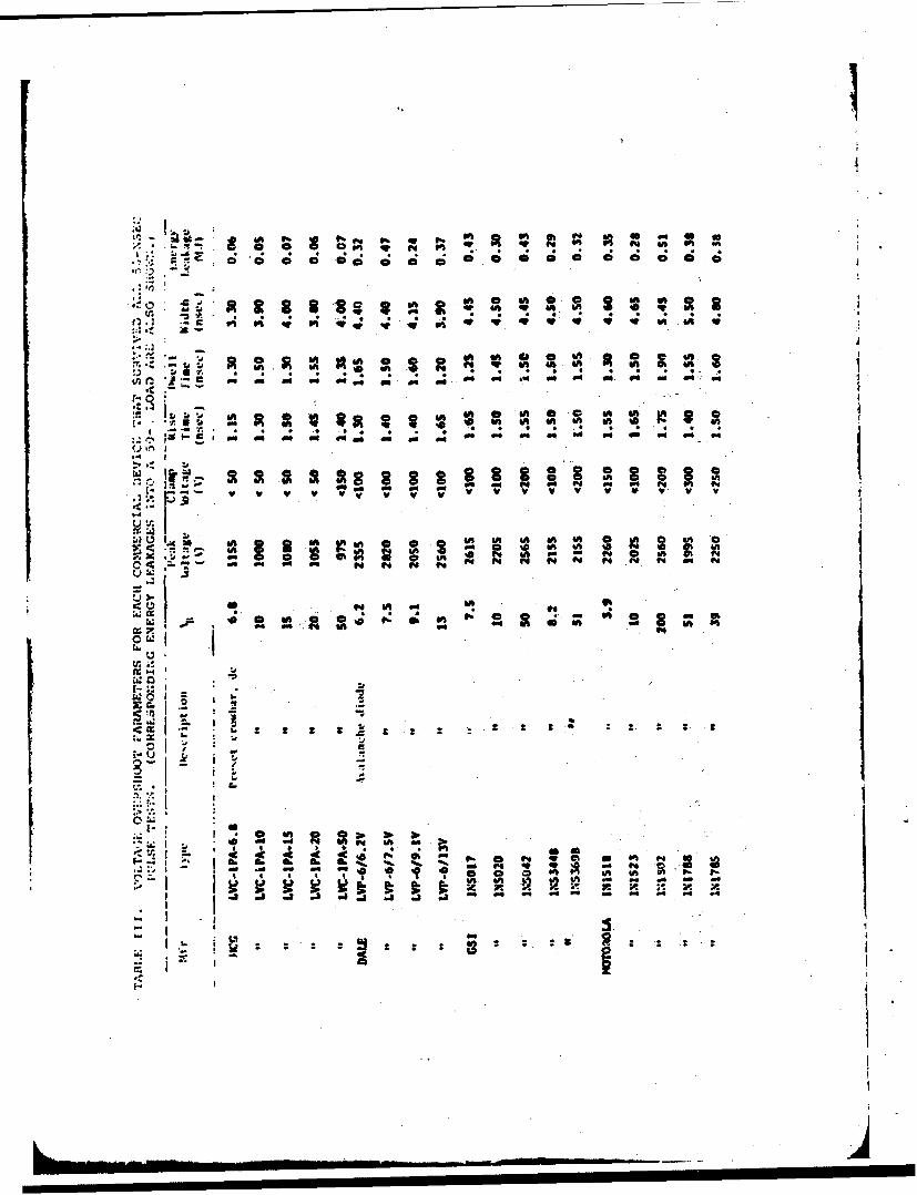
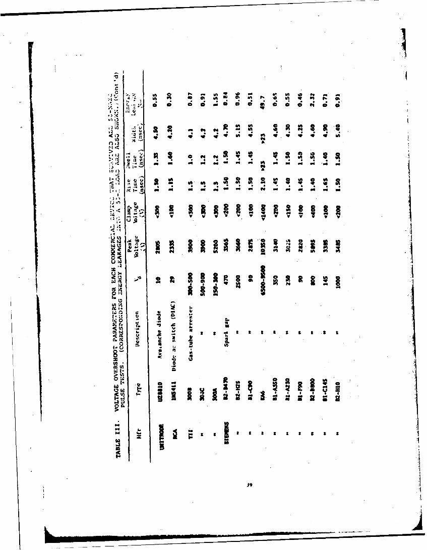
When a large, fast rise-time pulse was applied to a device, thetransmitted voltage momentarily exceeded, the rated breakdown voltage ofthe device, often by several kilovolts. This excess voltage, generallyreferred to as overshoot, depends on the overall response time of thetest system. Operationally, the response time must include the effectsof lead inductances--as these cannot be completely separated from thedevice--and of the test appatatus in addition to the inhere-It responsetime of the device. Zn these tests, the devices were rwurted in a waythat would minimize the effects of leads and test fixture, which ispresumably the way they would be mountrd in practice. Since thesecontributions are not easily separated, the overall response time is therelevant parameter.
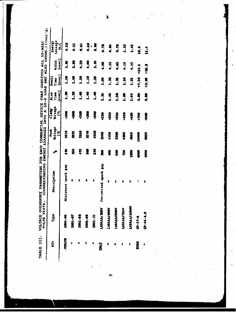
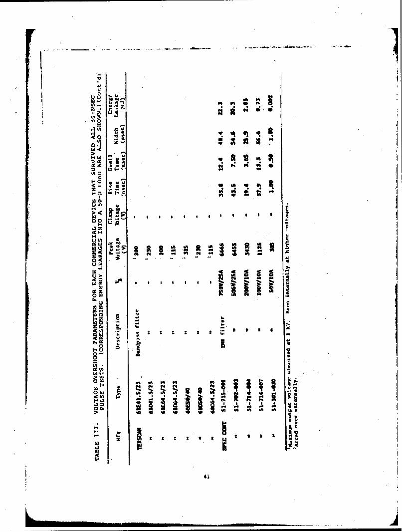
Response time was defined for these tests as the differencebetween the time of arrival of an incident pulse and the time at whichthe overshoot decayed to one-half of its maximum value. This and otherr'elevant parameters are defined in figure 5 and tabulated Cor the 11-kVinput pulse in cable III.
All measured values in table III are averages over the sample ofthat device type. The clamp voltages axe given as upper bounds becausethey wure read from the same photographs as the peak voltages and couldnot be determined with greater accuracy.
37
V% do a00 00~4 S 0*
v Si v 9 v 5; v v v v v vi 4 v
0 0
A 2 fm 0 a44ac ~ ~~ .- N *4 t, P4 .VN ON
u ~ ~ ~ ~ ~ ~ ~~P I: 9.9-!- ~- i.
W. 4% 0 6 i g a v 4 e 4 4 .
a.. SID~ V4* ,
tr.
d ON Wi 4
R 4.1
I I4
a a
4A
-. . - 0 0 011 - - 1 0 1
~DiV r4
MO.,j Iac lit
C f4
U 00 U
It~ (a 4A4
040U - I
.41.
t* It It2 2 Im , '
5A
0 40
0 w0
tn 11*1f~d It 9 t I
d1
Lev090
11) + " S ; " --
Z+ C * *'I *
(-do
o* 0 . . I + 'a 'IA
,1,4 I II-
6AA
Waa
"" I 1 2 -
0dc
4r40
U3 0haL a
w f
£a0
IIL
i A
4.'04L)
'-40
- . .-.. - - .-- f4
0~ LO0.. e
> w " 0
4.11
u in
1a3H
0g R
W 2z0.H S. bF.4Z011
0.-*
~ 41
in
o- h '
0 'UI-u 44 44a
~5w ain
t t t a~28 a I
gon 4I
643 I i
VC ,0
J
TIME
RIE TIME t
DWELL TIME a t2*.1
WIDTH 0 t3
PULSE DURATION a r
V9 PEAK OVERSHOOT VOLTAGE
Vc CLAMP VOLTAGE Of ARC VOLTAGE
Figure S. Response time and overshoot p)arameters for terminalprotection devices.
Using measured values of these parameters for the first pulseincident on the device# it is possible to estimate the energy that leakspast the device into a 50-.. load. The results of such computations arealso displayed in table 1I1. Some words of caution are in order withrespect to these energy leakages. First, in our test apparatus and tosome degree in all real systems, there are reflections at variouspoints, so that more than one pulse will be incident on the device. Inour case, the second pulse was larger than the first, oft1en by a factorof 2 or 3. Second, the total heating effect on a semiconductorjunction, due to, all the leakage pulses, will to some extent becumulative. This effect will, of course, depend on the separation ofthe pulsos, because of junction cooling between pulses and, thus, on thedetails of a particular system. At the. very least the .energy-leakagedata of table III provide a convenient basis of comparison for thevarious devices tested. The. method used to calculate these leakage datais given in dppendix B. Note that both peak voltage and energy leakageare greater for spark gaps than for most other devices.
|I 4 2

4.1.4 Clamp Level
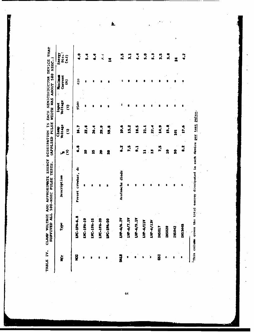
The effectiveness of a protectiva device is determined in part byits ability to limit the transmitted voltage after the initialovershoot. Thus, the clamp levels of all semiconductor devices thatsurvived all 500-nsec pulse tests were measured under similarconditiorLs. The results are given in table IV. Note that the actualvoltage drops are often more than twice the'rated breakdown voltage.The energy dissipation in table IV is the produet of the maximum currentand the breakdown voltage, Va, which was used for this calculationinstead of the clamp voltage. The result is a more conservativeestimate of the energy dissipation capacit':' of that particular device.
4.2 Derivable Quantities
To evaluate the protection offered by a given TPD to a particularcircuit with a specified threat level, it is necessary to consider the Acombination of, protector and protected circuit in considerably moredetail. This can be done in principle by applying the specified threat Ito the TPD and using the resulting time-domain waveforms to obtain anequivalent gcnerator for the TPD* This equivalent generator can then beapplied to the protected components, and the energy dissipation in eachof these components can be evaluated. By this time, there are adequatedata from which a prediction of either damage or no damage can be made.A method of obtaining the equivalent circuit of the TPD is given inappendix C. A method for predicting junction damage is given inappendix D and extended to the case of multiple pulses.
4.3 Discussion of Devices
This section summarizes the conclusions obtained from this studyrelevant to the suitability of various devhces as TPD's.
4.3.1 spark Gapoe
Spark gaps still appear to be among the main bulwarks againstintrusion of large FP surges. They are the only protection necessaryin some systems. In other systems, they are the only protectors Iwnowavailable with sufficiently small insertion loss.
Spark gaps are available with d-c breakdown voltages varying fromabout 90 to more than 10,000. The addition of radioactive gases andelectrode materials has evidently permitted much faster and moreconsistont arc formation. These materials can be made withlinterelectrode capacitances cI pF, so that circuit loading is small.Furthermore, they are virtually indestructible by a single EMPtransient, with current ratings typi!ally of 10 kA for severalmicroseconds.
43
.13k
W a .9 0 U t 9 a
u a
.4 w. 2 r o 00 ( l ,
64
on St8 3S 3 3 3 3
-In. -
* .. S ..
04 1
.43
(ne. I.44
X 1
0 f.0
n.44
u~n.
lb j
IIu
tm .
LA~ *IJ I eco'16 .
>.,
> C
tn -0

All of the spark gaps tested in this program appear about equallyeffective for E'P protection. This does not mean that they areequivalent, merely that our test methods could not distinguish betweerthem. The principal drawbacks to using spark gaps are the high d-cbreakdown voltave and ýthe relatively high-energy leakage, especiallywith small overvoltages.
4.3.2 Filters
Two types of filters--bandpasa and low pass--were evaluated. Inthe former category only two different kinds of device were tested. Themicrowave bandpass filters made by Texacan appeared able to handle the
test pulses without damage, and the transmitted voltage waves weresmall, largely because of arcing somewhere in the drvice. Such a filterwith a relatively narrow passband would probably give adequateprotect on for some systems.
Of the several low-pass filters tested, only the MIFI filters madeby .61£ctrum Control appeared to be undamaged. Generally opeaking, theseilit.%:r.j massed relatively large amounts of enerqy. If low leakage is
necessary these filters would have to be used in conjunction with orreplaced by some other device.
4.3.3 Avalanche Diodes
The avalanche diodes comprise the last major category of devicessuitable for terminal protection. oenerally speaking, only diodes withlow-breakdown voltages car, handle the necessary energy, ax)d these diodeshave such high-insertion loss as to make them useful only at lowfrequencies.
There is o.ao scheme for reducing insertion loss of a diode. ' Thismethod, however, yields a somewhat slower response to a large transientand is ineffective for signal voltages that exceed t1•- forward barrierpot,,ntial of the compensating diode.
Avalanche diodes can be used extensively to protect low-vultage,low-frequency circuits. Some low-capa citance (microwave) diodes olschave potential ir, ccmbinarion with other devices that will ihandle mostof the energy, leaving the diodc to providu fast clamping of relativelylow-level signals in high-freqjuency circuits.
-Clark, 0. M. and Winters, R. D., General Semiconductor Irdurtr:...;,Inc, "Foasiblllty Study for EMP Te~rminal Protection," rinal Rieort,Contract No. DAAG39-72-C-0044.
.JU
S. .... .... ..

4.3.4 Miscellaneous Semiconductor Devices
A number of specidl devices, such as diode a-c switches (DIAC's),crowbars, biasud suppressors, silicon-controlled ructifiers iSCk's),thyristors and pin diodes are, in general, of. little use for varyingroasons. A few of the 4CG preset crowbars and the RCA DIAC~s survivedthe pulse tests. Of these, only the DIAC has acceptably low insertion
* loss above a few hundred kilohertz.
* 5. CONCLUSIONS
* IThe collection of devices that survived all specified pulse testsSprincipally includes all spark gaps, some bandpass filters, most
avalanchi diodes with breakdown voltages less than about 50, and a fewmiscellaneous semiconductor devices with breakdown voltages also lessthan about 50. The dividing line near 50 V is, no doubt, a function ofthe maximum current and -pulse width used. The devices that survivedapplication of an l1-kV, 500-nsec pulse include almost all survivors ofthe 50-nsec pulsu test.
Of the devices that survived both pulse tests, only Spark gapshave acceptably low-insertion Joss over the frequency tange from 0 to100 MHz. Therefore, if wide-band protection is needed at the upper endof or beyond the above range, it can at predent be provided only byspark gaps.
spark gaps frequently fire slowiy and erratically at overvoltagesof loss than 2 or 3 times the d-c breakdown voltage. For this reason,they often allow greater energy leakage for small overvoltages than forlarge overvoltages. Also, becauue of the arc formation time, spark gapsgenerally pass somewhat more energy--even when significantlyovervolted--than do semiconductor devices, which respond rather rapidly.
The speed of response of each devicte depends strongly on themethod of installation. In fact, examination of table III suggests thatthe overall response is dominated by such things as lead inductance andthe impudance masmatch offered by the test chamber. Other tests haveshown that lead inductance is the more imvportant. It is therefore ofutmost importance to provide the shortest passible shunt paths fortransient currents (except in the case of filters). This implies verysmall TPD packages with short or no leads.
The bjndpass microwave filters manufacturod by Texacan offersubstantial [protection, and these or similar fY Iters :.,xy be useful wherewide-band response is not necessary.
17

II
6a RECOMMENDATIONS
6.1 Individual Devices
When further pulse tests are undertaken, a few carefully selecteddevices should be examined more closely so that the relevant parameters-can be detvlrrined with greater precision. Tho large number of devicesused in a survey of this nature does not permit adequate time to test a,statistically significant number of each tjp.
Future experiments should be planned carefully so that the deviceparameters in the high conduction mode can be derived from the pulsedata. These parameters are essential for predicting damage to protectedcircuits.
A diligent search should be made for. a low capacitance deviceusable at frequencies extending through and somewhat beyond the VHFrange. Such a device could supplement or replace the spark gap in manyapplications.
The usefulness of bandpass filters should be investigated more1
carefully. This will probably require some sort of survey of the
bandwidth requirements of military systems.
6.2 Combination# of Devices
It is likely that to existing single device can provide adequateprotection for some systems. The alterndL"."- in a combination ofdevices that complement each other so that the ,,W! i.. :'..-tionresults. .Generally speaking, the combination must have low-insertionloss, be relatively unsusceptible to damage, and provide rapid responseto transients, with good voltage clamping ability.
The spark gal) appears to be a vital part of any such mixture. Itcan be put in fr6nt of some other device without changing the overallfrequency response, while lending its hardness to the whole. The idea.is to make the gap fire rnpidly, and this usually means a largeovervoltage.
Preliminary tests indicate that a spark gap followed by a filtercan in some cases provide excellent transient protection for thefollowing reasonst
(a) The frequency content of the input is drastically alteredwhen the spark gap fires. Thus, when the transient is large enough tofire the gap, the energy left in the filter passband may be small, eventhough the frequency distribution of the original transient was stronglyconcentrated in the filter passband.
48

I(b) Before the spark gal fires, it can be strongly affected by
the portion of the transient that is reflected from the filter. Thefilter will, in general, refl,.ct a wave composed mainly of frequencieswell outside its passband. For such frequencies, the coeificient of
reflection for the incident voltage from the filter is essentially +1.The reflected signal will than add constructively to the input signalacross the spark gap and speed its turnon. Naturally, the physicalseparation between spark gap and filter should be small.
The most difficult case for this combination to handle will bewhen the input transient is concentrated in the filter pasaband, but thevoltage is not large enough to trigger the spark gap during any one-halfcycle. P is would occur, for example, with a damped sine wave of theform Ae sinwt, where w is in the filter passband, . is not too large,and A is only a few hundred volts. Even in this case, however, thefilter output impedance is still roughly that of the input -line, whichmay be large enough to limit the output current to a tolerable value.
It is therefore recommended that the effectiveness of this andother device combinations be determined.
4 9

APPENDIX A.--AN ANALYTICAL MODEL FOR THE FAST PULSER USED IN COMPONENTTESTING
Transmission lines may be analyzed by using methods that fall intoone of two groups. The niethods of the first group use electric circuittheory and have the advantage of analytical simplicity. The patametervalues and the conditions under which the resulting equations are
applicable, however, must be derived separdtely.
The methods of the second group depend on electromagnetic theory.They have the advantage of depending directly on the most fundamaentalprinciples of macroscopic eluctrodynamics. These methods also provideall necessary restrictions and 1Ir;x, L,1:.`ý and givt? the parametervalues.
Either procedure ultimately results in a pair of coupledfirst-order equations relating the current and voltage at a particularpoint on the line. Assuming that the line is balanced--that is, thereis no coumon-mode current, the fundamental transmission-line equationsare
-- 4 NI- -
*, F+1? - "I
where i - i(x,t) - current in each cunductor,
e- e(x0t) = potential diffur:ncu between conductors,
L a inductance per unit length,
k = ro:si.tanc,! per unit Ltn.gth,
C c CapacaitJ:;cnto r wi l
G co.nductan.x* pe~r unit leri;Ui..
This appendix follows closely th,. trc'atra..:t by o1Jmx1in, l|ijaýctransforming the above, equtt ions lead., to
(1.. + I: ) -.. - , + t',;:,+
:.oldman, Stanford, "Lanlece Tra.nsorm The;ry and Ulvrtrical'Transients," Dover, NJ, 114.).
Preemding page bank
APPENDIX A
These equations are still coupled. Differentiating and substitutinggive
* (l.s + R) (Cs + ie(xo)- . (Cs + ; )i(x,o)
-2E .( + R )(Cs r ,) F. - i, - C (Ls + R )6ex,o)x (9 R C+rE
Let n - ((Ls +. R) (Cs + G))I . Then the complementary solutions (to
the homogeneous equations) are II(x,s) Ale'nx + Benx
-nx mxE(x,s) = A2 e + 82e
If we assume no current or voltage on the laine at t - 0, thecomplementary function-, provide a complete solution.
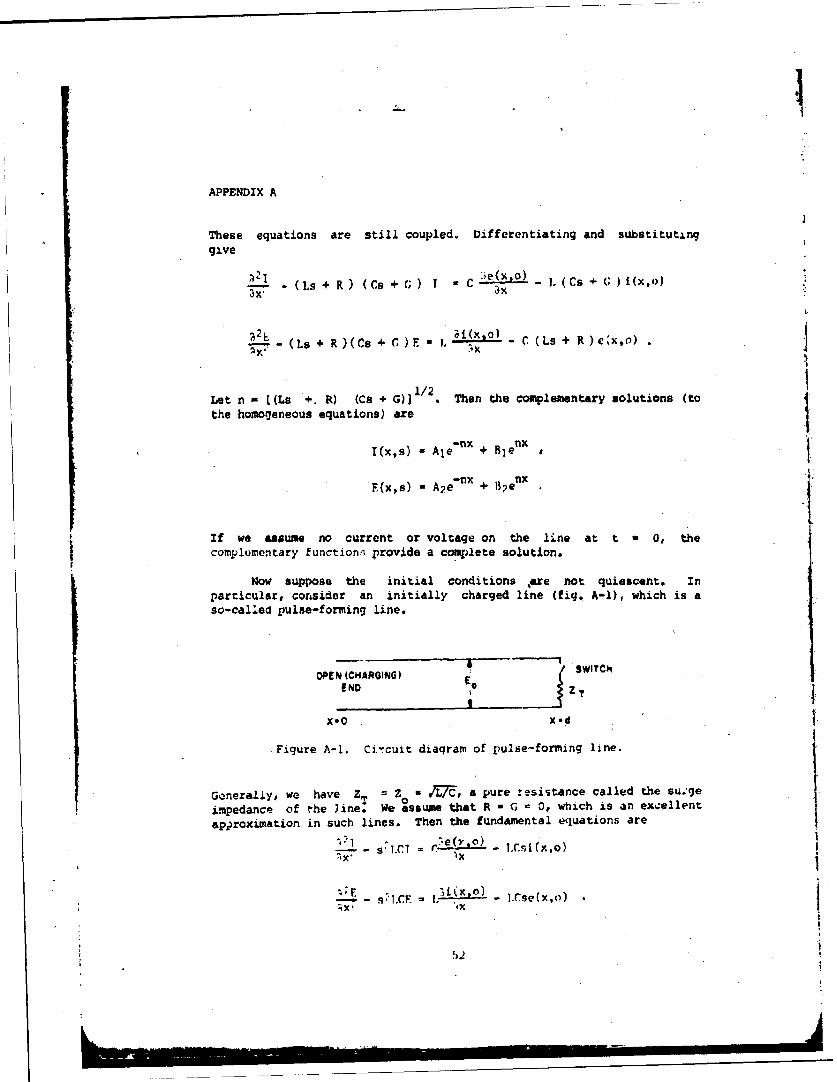
Now suppose the initial conditions are not quiescent. Inparticular, consider an initially charged line (fig. A-i), which is aso-called pulse-forming line.
OPEN (CHARGING) (SWICIM
END jZ
X8O X-"d
Figure A-I. Ci-ýcuit diaqram of pulse-forming line.
Generally, we have Z, = Zo 0 JL7* , a pure resistance called the su.'geimpedance of the Jine: We assume that R - G = 0, which is an excellentaproximation in such lines. Then the fundamental equations are
11 e (Y",- s1CI= -~(•
L(AKO)- -
-.

APPENDIX A
Prior to time t. 0, we' have
e f x , Nl a 1 :" ,
which impil' ,ls;) that
Thus, our equationis .simtPlify to
C. - i I :i
B.. standard w:thiod., 'f .wolvinq differential.. equation.'s with constantCoefficients, we find
I× . = A,. ' + B
'×, = A, -': ; ;•
:.•,'.. From t, form of the fundaj,.zntal eo4uations in thisj:.:.r ~xirn6itiz&%, we, know t."-at
.I,..vf-rt f•i in.. "t.:;,4!;.... . ..
From t..c initial :uilditlun .at x
A. -
:I
APPENDIX A
At the other end, for t :0 0, we have
1(d,t) 7 ) u•/K.(Cl.t)70
which has the trarsform
Our solutions at this end become
W(d,s) , AG-nt - i
.E(d,s) A . , -r( c + Vd+
Using these thre, relations at 9 - d wu easily find that
Al
2IThe solutions &n the •r•ijuenrýy domain are, theruiore,
1- 7 - W
Thesu ar.: r,:ad.l'.' transformi,.d .,k inte) Ukt time domalini. The- rusults
I I II -, I - ,.,,I
! I f t t - "Yr' )i
:j

APPENiDIX A
where U(t) is a unit step function having thc property
I, t 0
The current consists of two stot) functions that have opposite
signs and travel in opposite directions. The first step starts atx - d, t 0, and movos to the left. The second step becjins at x - 0,t m d/V-C, and Imoves to the right, reancellincj tU first as it moves. Thenet effect is the life history ihown in figure A-2.
X&O Xed
SL
XSO X'd
Fi1i re A- . :.i'.' i;t. r'.. . :ur : ' ,¢,.Vt' i:, i ..- r rl i:,c: I ;.,.-
"T!ni: wav.:fr,•Int trdv ili ng t:) LiUs 1.ft c II; ý,;1,d DMt i d to b,.,r-:lt:. :t;.| f•t ,m tilt: O I.L:', Cild Wit; i .a ,Ii.anlj In .;i,! i. All ,;tortvd
.1 .....Z -i
x
APPENDIX A
The appropriate reflection coefficients are given in a nuuxer ofstandard texts. For voltage,
7.I - 7
R 0
* ' 7..r+ 7o
and for current,:' -:'
0 TR,' 7. + / ' I'
where ZT is the actual terminating impedance. In the simple cases
considertd here, we have either ZZ or Z = . The conset3pentrefleCtion cOUf~iciVI'Ls follow imm'dIately.
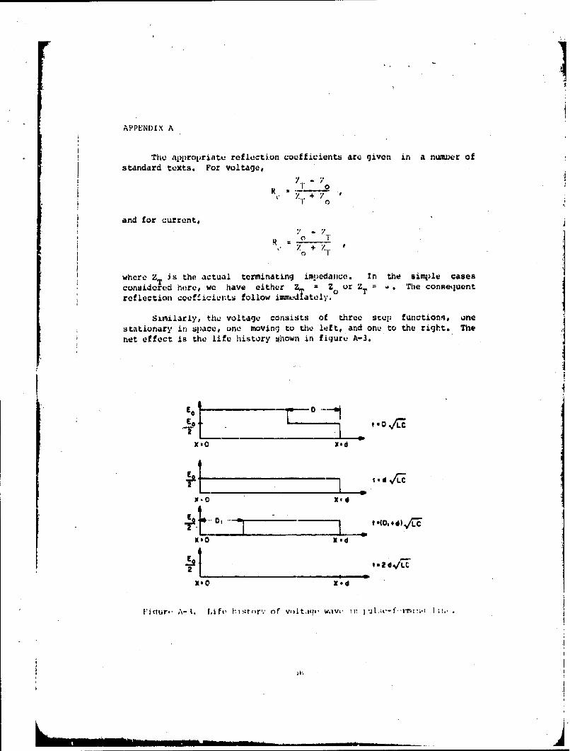
Similarly, the voltage consists of three scep functions, onestationary in space, one moving to t•e lfet, and one to the right. The
net effect is the life history shown in figurte A-3.
X8O Xedi
2 4
X-O X,€l
-/L
2~t P2 d,/LC
XOO Xed
V'i tur'' A- 4. Lifv t or' . of Vr)1t,aqo- w.-tV" !r1 1 '1 -f '-rMn-I:; I
i )U.
IIAPPENDIX A
In this example, the observed voltage at the terminating end in never
cjreator thlan E /2.
The energy initially stored in such a line is
=. ((:d)F 2
On the uther hand, if T 2d.L't is the duration of the piulse, the energy-
dissipated in R is
"RT :(
which is, of coirac, in accord with the principle of conservation ofenergy.
For a coaxial line with air dielectric, the above formulation is
valid provided that . << A, whure a is the i.d. of the outer
conductor, and A is the 4hortest wavelenqtf of interest.
APPENDIX B.--CALCULATION OF ENERGY LEAKAGL THROUGH TPD INTO A M4ATCHEDLOAD FROM A PULSED INPUT
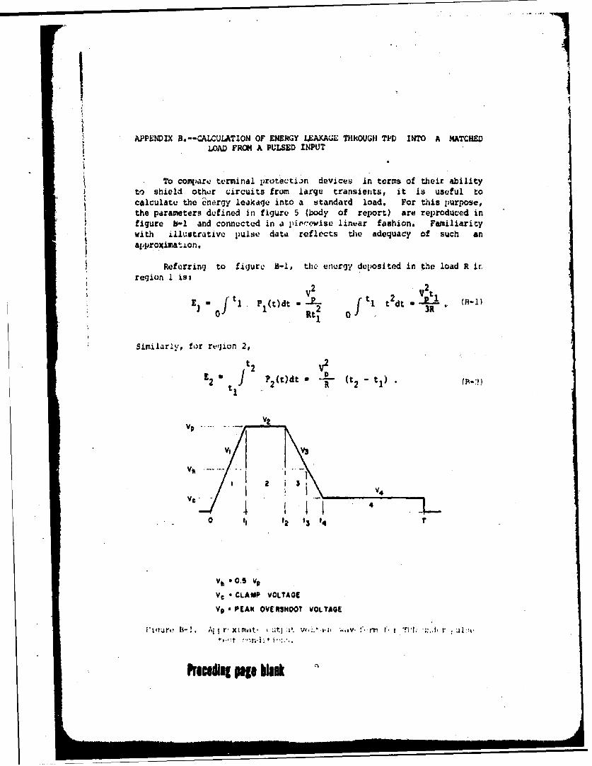
To compare terminal protectiin devices in terms of their abilityto shield other circuits from large transients, it is useful tocalculate the e nergy ieakdae into a standard load. For this purpose,the parameters defined in figure 5 (Ibody of report) are reproduced infigure b-l and connected in a 1ireoowise linear fashion. Familiaritywith illu:strative pulse data reflects the adequacy of such anapproximalt.Lon.
Referring to figure 8-1, tho energy deposited in the load R ir.region I is,
V2t 2 v2
E_ 1 Pt (t)ddt 2 1 CR-I)1 - Rt 1 2. 3R
Similarly, for rt•Jion 2 ,
E 2 P2 (td aV2-
P (~dt --!- (t2 t)
A V O2Vt V
Vp ........ OVERHOT OLA
Vt. • .-
Vt a CLAMP VOLTAGE
Vp• a PEAK OVE*9HOOT VOLTAGE
"i ,'ture 14-!. Al. 1 r' XImait., it .1j. vI. ri. .i .; V' " i ' t I"•.ll ;. . : :4.
Prceitln page hglnk
APPENDIX B
To evaluate E,, we first need V and t4 in terms of. known quantities.It is easy to discover that
V it -t2AV3 (t) -v - " t t (C t4- P (t 3- t 2 2
t2 +2 (t3 -t 2) v Hivp
The energy E3 iL. then
9 3 I -t 2 d .(114)
3 2 4.t" [3 t 2)J
i
A simple change of variable gives
4V2 [.-t V 123 I du
E3 "V (V--c (t3-t1 + 3
3~~~~ 3 -2
pp2(V,3-Vý3)
3 3V R (t3-t2)'
In region 4 ,
• , f 4 (t)dt. -- i-titI(
4 " [t V -t 2"2(t 3-t 2 1
4 R 2-
APPENDIX B
Adding all four components gives the total energy leakage into the loadfor one pulse.
E 3R R 2 p. 3-t 2)
+ .C (V 0-v)
This can be simplified further for the cases at hand--that i3, at thehighest input voltages. Here, we always have Vr, > 5V ; and in mostS' ~C.cases we have V > 10 V... Hence, we can safel' ignore Vi in complarisonto V . Also* sfnce the Vý term is smdil, we cin approximate it with aimorevgonerous estima'te by Cdropping all times ex~elpt
Then the approximate total energy leakage is
V t V 2V2 2.1" + _-I ti +. . uI-s;R (2 91 + 3R I 3 t) 3 R
jince neither t. nor t •-t wa- directly measured, this can be writtenin the more zoiveniezlt form
E I- (t2 - tii - t+ 2t3
The term t - t L . ,.*,: in'a:t 1v--uai. it was directly measured, alongwith t # t' , aind 't.
All tim,.:i wq&',:, reurded irn ndnouseonds thus, if we want £ in)oult.s, aill trms maxt be multiplied by 10-'1.

APPENDIX C.--ANALYSIS OF VQUIVAL.ENT CIRCUIT OF A VIODE UN1kk TEST CONDITIONS
A model for ai Zenur diode installed in a test s'ystem with intrimcnalimpedance R~ is shown in fiLlure C-.L. Otnetr muduL:s haive been used forvarious freqjuency raincus and conditions of bias. This particular model
d~aj~r&; to be tht: sipicpst one~ which is -advuatu for the large-sign~alvasu. The following trcatmentn, .&da.ptod from tha~t (Ii2."vfl by ~Jui.Jin ut s4l
su'Jalcsts how M,: 1,ar mtaor, miijht b,. durivod whin .adavauaitu. experimental
data art: avaiIl&biu. ot:iur dv.;migjht bK' more or less tr~actablcO t.h.nVicL diode.I
-4vC diodt, :.y1v~) -1~ t.ar -in -1 .. u.ldode t - t
1ýI hu; I cro iLnI-eci.i:,.:t wiivt furwdrd bias,:J, i sif inji tv i~modance* forNt(j1;t1VQ W-iL5 nc;tw0L':; "Ole ad V,,, Aaud Lt. -AJ ''.1.t ItS impvdx.gtv so thatt!.v V:.t.qtivt: Liar;i nt.Vvr 41X- ii'JS V%.. t j lun.-.:tion ea~~t.ar.,..u, C , i s.As:: =nwJ tu bc t~ht .. %q a:i t.ari.:te aLt rk%:
Wiut.1h i a lx)sitiVt LUUl.;t (1t.~...~ ~ .ac' clpi-11ic t.. this dioide,tht: Zueir junlction' LS .c) .sdri .%7 : ~ .:~fir.*uit ui.L., th.' brvuakdtaw:
Wher brvakliown o,%urs thtc volt .atup- u::4Ii
it. Should bie pui:nLi.d (jut thIAt. t11V -.*1di I Of 1intutcZ.'t, 6.L.t. ,
faj.;t rise time -au.l~t'. wt'th. VqOr~ t-ý ti.`;n--, izdvz.-; cif maqnitud.' grvt,.vtrtnan VJ, are su,;h that tliv 4ncidunt vvltaq.;-. vxc-v~is V-. aft...z it
* f .a ~ * Hon.:v, it sh,)41j J i w ) . : ta. *.r...t 0 h; .; n)un I :..
1.4 -owi s l ' Ie Iintu.ir , thjat. i , t nj:*i d~
:n,.a.i~i r~j tiffle Wn.*.1v t;~ ci ~j. I, f'.11 .*u.01AL~, :t.. Mt~, a VCLs .;a. 7h
.1 6 YA 4 h.*.'ur.A te ju.r'4 ta t;x r. I
L.:1. : r . .. .Jr : .i. 1 .e. j~V ~ t % I. k,*r,
Prrnig pop Nook
I I.* II
APPENDIX C
L
V( It
Figure C-1. Equivalent circuit for Zener diode under t,.t conditions.
RL
;,t WOt
v,,,( t, #ft i
C 3 T -Fitiurt, C.-2. Reiuced v.,uivwvl!:t circuit fc'r ;'ener dir'd,, utnd, r tw.;t
The lool: vlItarq.i ft'r the ý.irvuat of ftgurv C-- aria
(R + r)1 1 + L (t rl2 - 1,d- V * t)
-ri - L d -1 + (R+r)i 2 + L dt - 0 •
The L-aj.lizeu transforms of thesu ,irv
(R + r + Ls) 1I (s) - (r + I.m) 1, (OR) -V (s)
- (r + .s) 1 (s) + (R + r + Ls) 1, (.) • 0
SolvLing for tho' juIl.ut :,jrr. :;t I;ivt:,
V (s) (r + Ls)
2 +r
APPENDix c
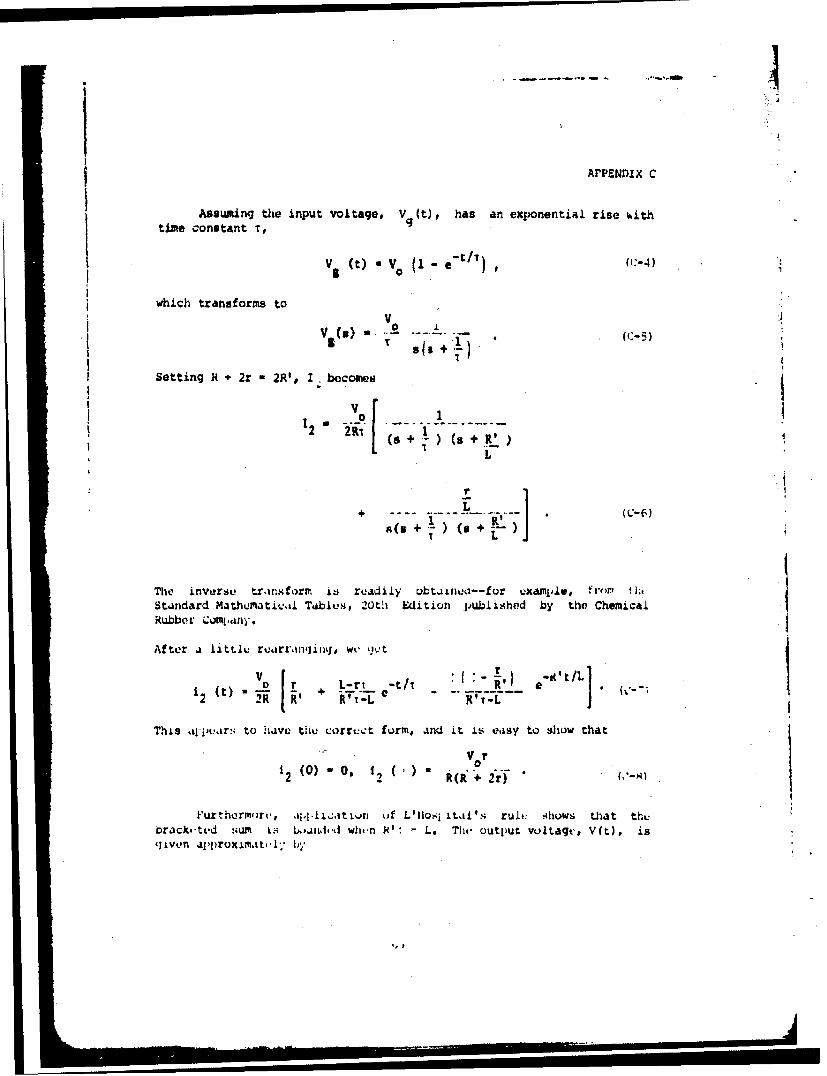
Assuming the input voltage, V Mt, has an exp~onential rise 6ith
timte constant r, (9 1- tI
which transforms to :
Setting R + 2r *2R', I becometo
2 M11 (s + )(+ R,
LL
The inverse tran:sform is readily obta~unoi-for ux~amjui, IrorttimSta.ndard Mathemativ.&I Tdble~s, 20th Edition published by the Chemical
After a littiv ruaracltq -o ( 1vt .'/L
This a&Ipua~rs; to haive tihe corrt:%:t turn, and it i-. ea&sy to shuw that
1 (0) -0 , 1 () V 0
Furthermortv, ak;.IiJ,..tw.nr of L'l~os.q ILai's rult: shuws that tht:brack.-tcd sum is ,IjmiiqtA whtwn R." L. Tliv output vultage, V(t), is

j APENT ~ WOc R11 (t) Vz
V( R ,+ r2 i1 e-t/ R'J -~R't1.I+ V
This lia~s tho foliowaintlJ imimt-;
y rV(0)V - 0, V(.)u 2 R,- + V
Tile uxare .~,uon for tihu. '.utput Voi -ti, s~: mp;:lyJiftied b",~~~~ir:'tht: jljrPI3IarJuItt Vk1i utAIUL'ýU U'lur..a1*n'*tmvr'i.
R 50. r'
L -10-50
* ,. ~~R' R+r f
1. rR/ JV ~ V, [ V. &-.~-~
"I, n 1 , I-* - Ir U . f: I' oI. 1i 1 b y f I t : ' '. . *. 1 t il:v
I;± to *:rc i x-* : known L w .-if L. ria' i I . .i-w I . 1 b'1v r ~ . : t: h.! I
i, u ji~ ,' k:.ir % w ;*i.1*:;. 1, J r, 0- 1~: ht -. "Iat' 1, IVa :t t :.j I f
JV.-i I''.. ý
I;'Z~ .)ti.V..i;.l a: L, :m.qjl. I I: v.iri.ttia.-. ii: r, it i.s ns-,*e 's.Iry
t L moa.~~rvc )!I*-:1.it i:.L I i ,V U::. t. ~ La. Ia Xz XAr~t:.: Wt 1. IVL
V~~t)~ R-L1. -/1- R/L
WO'

Sic R ad V kr,., known, the~ 'probiU~n L; tu fi ii vailuc!; of an~d L So,thatt this ~ c:r:;io:~ t fit:; the obero f )r[n.
Whdt 1 1 inut'd, of hi.w~c 1,;~'r 1. !w tor fur tht. TWV
getno.rator to ti,.k j;rotvi:tvJ cLrcuL t.; t,) '~~t:U LIU: ruOf!fe~red by thi, T111) is wv-LiudttL-. T'he It'.-.vssry L.Lrcuit wayi cudusand smicorductor JaLm~age d.ttt arv avai aL, uiý;twhro, Appoi~ix V ofparenL r%2port lives a& method ustiful whoet.* multip1i ruf loctiuns must be

APPENDIX D.--THERMAL RESPONSE OF SLMICONLUCTOR JUNCTIONS UNULR APPLICATIONOF A SEQUENCE OF PULSES
D-1. INTRODUCTION
-n many electronic systems, an EMP-induced transient effectivelyconsists of a damped sequence of pulses. lhis condition arises eitherbecause of filtering inside the system, or because of multiplereflections from' discontinuities in signal transmission paths. Theresult is that not one pulse but a tv-tin of pulses is actually incidenton a given TPD0 Thus, since th',. i-!ating effect of the leakage pulses onprotected :ircuits is to some extent cumulative, multiple pulses mayraise t/a temperature of.a semiconductor junction to the failure point,even though any one pulse might not be nearly large enougn to do so.
A substantial amount of effort, both theoretical and ex'rer`-te.,tal,has been apj)lied to this problem in recent years. The ex.erimý.-.ij workhas consi-ted mainly of applying a uniform train of rectangulad )l•lsesto a device until it fails. The onset of fd'Llure ir generally an,,ouncedvy second breakdown. The theoveti.zal work has b;,'n mostly c"nfifnad tccalculations of temperature rise at certain points in the depletionregion. The general Iprocvdure is to assume somc model for th4
semiconductor and environs, withi hcit added homogeneously to the -
junction during -,Ach pulse. The inhomogenieuus diffusio:;. e:Iuation isthen solved for the chosen mode-', using values of thermal c.nductivityand diffusivity averaged :ver the expected temperature raneu. The "predict•,d junction temperature is compared with tU(: te0,n1xratur.Žneccs,.o ", or initiation of second brekdj•n, which-- fur unknownr-asoi.s--lius verv. near the intrinsic tum.n.raturu If tiu ,;cmi,:m nduttor.
Thi1. apperidix preuents the .•. by '•1ti ful a
single incident p[ls.4e and ,:xtundud by Frantk, 1 U.' , fur anarbLtrary nume-fr of pjulses ')f known ma-;nit.:|.:, width. "nd s,'i..Aration.1he solution is ad.:quate for all i;ulse widths zjrtaler theea ayx;ut I :secand the iulse train can be luitt! lc;n%, i,o-s:bi.y as long as 50 ,.seu,before thc heat sink chAnges ,';mperature aj.prU---ibly. Thu respottses tosinusoidal and damped sinusoidal inputs ar, aIlsu dis-:usst.d. Minnitil'spapers also give( a subttanti,0i bikdwqgrapihy of the fiid of #htx-malbreakdown -f semiconductor junl:tiozA.
-Minniti, P. J., Jr., "Devwlopment or a Se.xic-nd'.ctor Failure Model forLightninq Induced Ful ;os," MDAC-East Avionics "kch. Tnotv' Xv;' --''i *
Dec 1972.- Minniti, R. J. , Jr. , "Irvo!:t i Ci-t jo. : of St;cc:,nd | rvjkdt'.- 1i n
Semiconductor Junction Dev ices," MMAC--I- t Avu•r, Tn:n.. Note A7tN73-0-')2, ,hine 1973.
F'rar.kel, Kenneth A. , "?% Mcrle] for 5,'* 're, t'j"tr at ' J'- to theApp]ization of Mult il. Pulse;," Four-,:: A:.u, -iident Te.chnr.iralSymposium at HJI, lý-I'r A4jo 1)73.
69
Preceding page blank

APPENDITX 1)
The cuenural llflL' of davulopinent in thiS1 alipeiidiX ~t 'otufro th~ ~ip~u~t mod to Progrossively morv reiaJ.i..tic mcxk'ls. SQA,..;~ipi'Vu* well-k~nown maturiaj± has boun included tto mjkii 01v treaktmentrvoisunab.ly sof-containvd. We 4ru i~waite that. th.,, models omploy4Lsd Ih.Avedetect4 but hope tiat the rosuIlS indIicdte Ji viabiv WaY of treatingj tileeffect of multiple puls4es in .# cjivu,:. Sys'tcr..
Ir. has betni found that junctiuli dev~.ces undergo a phoisomenon kuowi~ se,.nd bro'akdown" before they fail. In second breakdown, thie a4.ViceLopvet.k~ in a~ hi'jh-currwnt modt, with j iOw-vi)ltaq,- drop. acrosu thejumntirm. Wber~ a device is in thu j'valanchu, iodL, it is buleJ.ved thatelev.~ted LMj~eratLrL;, will ca1usu currunt cons~trictions~ at dtefe.:ts i-. thejuntiot~oi. Tho IOC~i~lyý inc'euased curreit. denisity will furthor raist? thetaflieraturL. it the wu.!j points. Tnesv lou.il hot spots uan enlarqu, theýicuý-t, at~ ..an causu .iooal moltiricj, which may 1,..stroy thoý device.
So~nQ authors believu tha&t a dcvi,; will (qo into second broakdownwhenr aiiy wek :;pot. re.1chus tht* jntrimn~i; ttmpurat~re, of thu dcvi,:c. Att;1.1 tenjueratur.', the nriuj~er of imil~r~nsluc~ri~is eqju" to the lkwribur dut. to doping of thte -jv-icu~nductor. At t~i.!jinntrinsic tumpor.,ture, thu `-uflticin £JdrriLV can bu dst-ýruyvd at UluwCekk VIpUL, alnd MOSt Of thle Ciarcrit triL'.i wo (j throutgh thisi: rt-uioI 01low rusistamcve.
Exa minit.-oti of Lio. data for :-!u,;und lirUakdt.wn caunud by sinijit-pulso, dlj'it.ntr uraitiu:; shows. Limit thort: i. ofarjv.- i widt: range in; the',ower ncvdt.d t-j a.useon. sv vti ruakd.ow.) i..' of aj qivte:, typt.. Tjlu.;range of ten vari,.,. Lby L fa,. ttr (if )j*. thrvv, dald tlu Sproad isso)m#etjimus in o.rdor orf rlarjpiiudv. 3iucz, A :~r*i 1:; .IAtl 1- ijId-'...tj vLt!.At. any q.'pavral U, -4uydv*I ~. - *L'.:. a.!j-ýV~X UflL~ioi,.
710vo , mdtils- u:;.dr.:.~.;b .r.;,±:[ ar.jiJ:..uci ! tLu Iluwi j..;
D-Z 5F~j~. ).l*~~': ;.iAL: 'Am. N~ 1..;'ndJýULj~h VI-ý;*' N: :4E.;
C~ei:.rti;c. intiIt I shi)wLA ii, f~ ijar,~ )-I. TII simipl ified MUdeIVwill1 be U.'eiI ti. ±1l.u ;t '-.I UPi- McthkW if .;,juI uj ti, thv rosultU; of wiT
.tinruti , R... . ,'~comrtc.! ai ý%'ri I('ductor Failure Model for
VQ~c 1972.
seŽmi,:onduct-r .Iuni*tion e MIAC-I..; ;t. AVi oni:, T--r'- h Xotv. AT.N
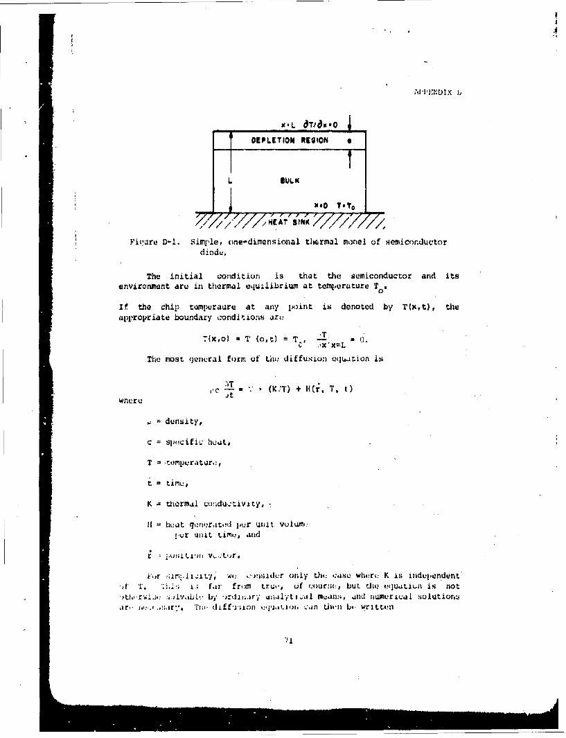
XEL d)T/6O0DEPLETION *940ON *
L UILK
'XO T'To
.Fiure D-i. Simple, one-dimensional thermal moriel of .emlconductordi ode.
The initial conditiuri is that the semiconductor and itsenvironment are in thermal equilibrium at temp~erature To.
If the chip tompuraure at any jx)int is denoted by T(x,t), tileappropriate boundary conditiorns arti
-(x,o) = T (o,t) T', .ix'X - 0.
The most jeneral forr. of tLho diffusion equuation is
IT - (KTI) + H(i, 'T t)where
density,
c = SC•ifijL huat,
T = ti.wpur~atur.,,
t= time,
K - thermal u,,ductivity,
II = huat gerraLt*,d pur unit. velujnIour unit timt:, and
V'•ir :;lrm. Ii .'it', w,4: o.'n;ithr only thti e:asu wh:r(: K is indepen.denti. "'i .; fazr fro}m trut,, uf c()ur!;e, but tho equ.aLitn is not
t.th.wi., :),/vdb[,' by; ",rdili.,r~' a~�'Anlyti..l mauan:i, and numLrical solutionsar.. i:-.:, .:;.ir'.,. Tn,. di ffz ;ion ,:,pi•tLig, ..-an tUin b,- writtevn
7j

APPENDIX D
L T •T +P
k '3t T + , (D-1)X
where
k - K/c thermal diffusivity,
P a power input,
a - depletion width, and
A - active arer.
Note that the equation now has no dependence on TO, so the solutionsgive the temperature rise, AT a T - To.
To solve the inhomogencous equation, we first solve tnehomogeneous equation
I 3T 'T (b-2-k )-t
where we assume that the chip is so large that the y and z clependencesof T can be ignored. Using the method o separation of variable3 weassume a solut.on of the form
tjT(x,t) a F(x)G(t),
and find
F - ScomBx + Csinhy, G a Ac kt
where A, s, and C ate constants of integratlon, and -07 is the ,separatton constd-it.
The boundary condition at x 0 implies thiat 9 - 0, ,and the otherboundary condition fixei, the values of ,'. We eauiiy fird that
Thus;, the general solution to.the hofm..:.q-neou, e, quitic'. i.;
nT~ -x:" kt jfl-t, tvl) - f).k, slii;x ,
no,
I = , , ,, ...... ... .. ..... ., ... ... . .7 -
wi~th cafl5toflts L,
The~ particula~r integral fo11c~w~ ns~ I aitf.,%moiie ?nof equation (D-1)~, viz týail rmaMd~e ý
.~.+ k*''
~4W e aasumeŽ solutic~n of the fort
eT - -' (LJs4Jfl
and a heat function of the formi
Puttir,9 thi'se into pt'iatic.rr (DI and us,*IjW t!)(, linecar indtepondurce o~f*si ±ir'x, P have frnr all r
Thij8 i~c Va-IIiv 'o Ivod uý; .c;tinq rt.~r~ n fa.r,, r
Wf C'I .,.(Xt '.el t7 2~ invert ing) *,;Iuatta Iu 'D-4) ia.nsugneA indlcv-urdt-nit .: t
I ~ ~ ~ ~ w *~JI(dc X

Putting this into the euiution for n and noting that : (0)
ki.
From equations (D-1) and 4D- 3) we se:' that
kil;aAK
so the terIperature rise is given by
21).., - " f - kt
minil'l;. minlr.a sinrix .(1)- 5)
for a rectangular pulse appl~lied at timo 0 and lasting until time t.This result h,-s recently been published Ly MJ.nniti, 1 '2 who also show.:dthat the time dependence reduces to
4a
.. 1.--.'it t I¢
!'raniki. 4. ** t i t In ' wia-; to~ txt(.ind, this rusut to th, C.AO~ (Ifrfect.Ar'(ular i iI .u.: f a trt I trary hv..iti;t , width, aind so'l, ratr,1. r.. Thesol ut iO t .tt, ti . nhyprtl','o, i;i " ffu: |iti ,.juation: was i.qiWv r; carlietr i 1
.. o .. .. ,. ,. , . .. I
I)," I * '.'
"; i ..', .A.Y..
. .,:,. ," ,:. .I .;, .. T.*.::. ,'," p v , j: . A... .... ..3 "9 .
74
AP'PENDIX 1)
this section. This solution, equation (D-5), was, of course, only the
particular integral, but in that case the complementary function waszero because the initial temperature difference was zero. Thus, thecomplementary function qoverns the temperature decay with no excitationpresent, while the particular interjral ioverns the temperature rise withexcitation.
Now suppose that the heat source is turned off at time ti theinitial condition is qiven by equation (D-5), with t - t j , and the sameboundary conditions exist as before. The .iolution to the heat equationfor this condition was previously given as
&T "n Dne''k siou.x•
no
Since the initial condition is alroxdy in Fourier series form, it. is.vident that the snlution at some later time, t., is
alAK n-l
'I
Further, suppose that the first p:ulse was of power PI and that att - t2 a pulse of power P., is al.1plied until t a t . Then we have
2 3
AT(xt 3) s i-1. -' . si..fn..a sin'.x
+ ,, I-_. k(t -t
If therft is no 1-ulsp until t t%,
7,3

r4
APPENDIX D
:, (x, t;, • ..... in..l. 41n: a sin,- x
+ • -,."tt).-t ,
+ P.(e-k
By now it should be easy to see how this goes. After N pulses, weshall have I 2
_.,._- . Iin:l. sin.'a slmn;x
Mn-1
And after a period of no pulse followinq N pulses.
) -k- -I-. 1 XT x,t.• aI.AK n-l ,H'
(t -ti
D-3. SOLUTION FOR N CYCLES OF A SiNE-WAVE INPUT, USING A SImPLEONE-DIMPNSIONAL MODEL
Iuppose the input voltage is in the form of a sinusoid. Thedevice .voltage is approximately zero wheti forward biased andapproximately V when reverse biased. The current is given by Isin..t and the power by P - I V sinwt. 0
Referring to section D-2, the equation to be solved is
n + k.': 'kA sin..t
where?I V,
A ...... n . l .' .
n7a. ):
APPENDIX D
iJsinq the same inteqratinq factor as before, we find that
m jc.~ ~-+ 'kt."k sin,-t - •.¢oM,;t + LO
The general solution is then given by
21 V q I n i. l-tai it, 1rx
- O.1.AK n-1 (.'kw + b
.ksln. t coixtit op ktI
for t -.1 , where is tho period of t..e sine wave.
After one-half period of such heating,
2k1 %I
ii].AK n-1
. V *4.."l'.'
And ,ifttr otn, l'urlod, wt- i'vw'
21 Vk. ' -�N'" s f n. I.s ,n :i1,•I.. x
tl.AK A-*I1- I
A k.~Ii-
-~ ~e W- W. : thl,kt no vvrcy is jd,d. ,g.;i tiit jurc•. nni ji; fcorward
In ,,n,.-r.al, af,.r N + ,ir.,'-' lf 1 .eriaod-,
,. . -. I ) ., I+
~ -_
r
APPENDIX D
whereas after N periods,
21 0Vk'I)'
..'•L.in.-.--"i. ii sin, !
77 +
D-4. SOLUTION FOR N CYCLES OF A DAMPED SI:NE-WAVE INPUT, USING A SIMPLEONE- DI %JENS I ONAL MODEL
Suppose the input is a damped -4iri.%wave. The problem is similarto that of section D-3, except we take
1 I - l * *t .sn.t ,
so that the equation to be solwiad is
d : .'-' kA t
(it n A
where A s tise -dMt- a.; ir section D-3. Th,, r,,slt iL
-" kt s. 111'-' l . t - , ,. t
This has.i almoyst th- admc form i.- for th," .4ili., wlvc., th, difftronflut bu'iv:;
maILnly that the 6"'k terms of t~ht' LntuqIr id .are rnI-ict'ed b'y ;1k-
Aftr n,-half ,this bom,:
n ( 'k-:)+ ."
+J

7 +
4tt ~t ý; kjod l " t l
.'1 v
b i ll.; s l- I i a- I ) ,
k..
APPENDIX P
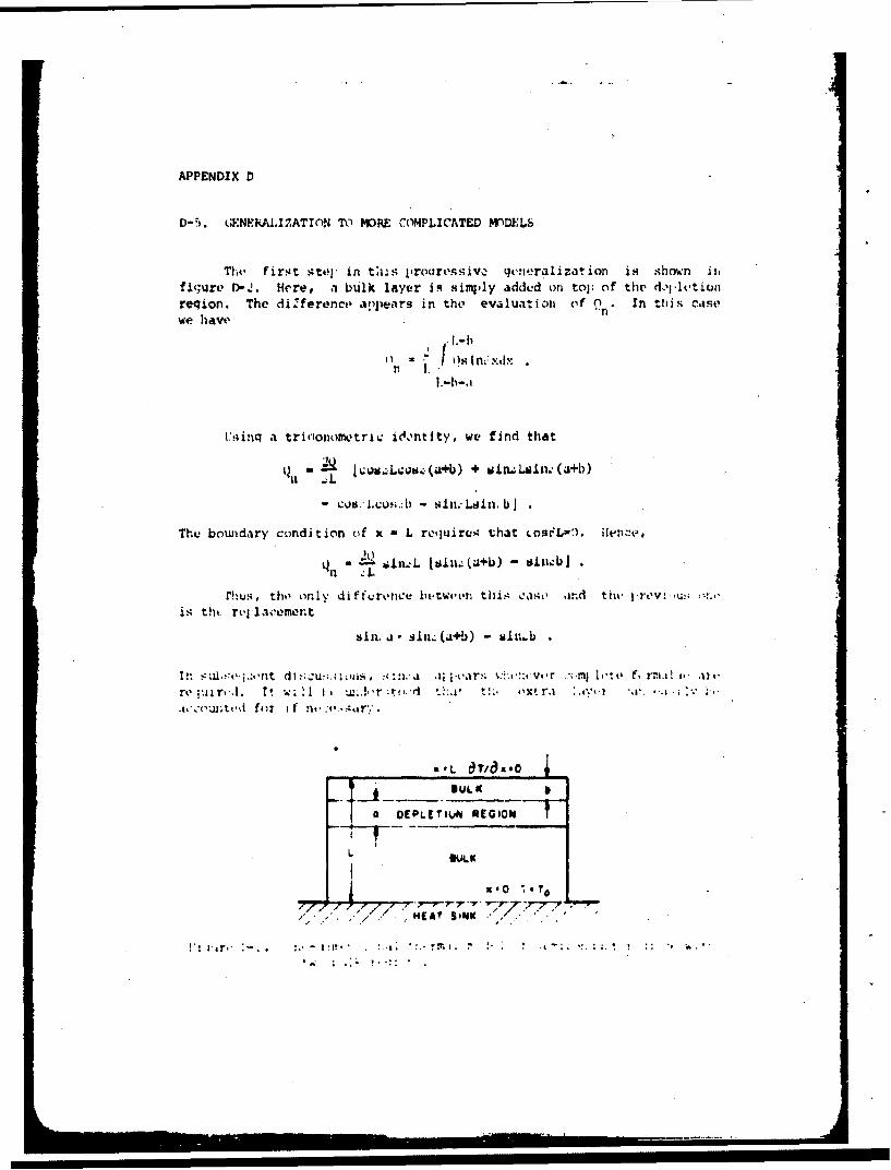
D-"). GEN!:kALX7.ATION TV 1MORE COMPLICATED W~DELS
The fir-At stl in t'ai prouressiva cqeneralizat iof is ;hcmnf its~ficqurc D-.J. licre, *I bualk layer iq sivj'Iy aidded oni tolp of the di'l-vtionreqion. The dillerienct, appears in tht, evaluation (if On . In this ca.se'we have
t:sinq a trivio noikstr1i% iclntity, we find that
- ;'Qlo.Lcu(.;a+b) + ~h.~.ML~1bn L
The~ boundary condition (if x m L r~t~luiruo, that LosiFLu0. iIt'n:)t:e
Fhus , tho onl 1y difful2ronc lietw'evi- th~i- Laso vnd t ht, -*V-:is thL' rvilav!ement
Sill. a sill.; (~a+b) - uin.J.
In.4 i ý~I: v Ilt d I U ou. isni., a* .n I .i ~I v r' s t:: :i vir -m 1 vt f\ rm .21I - .11,
L'
L[A SINK
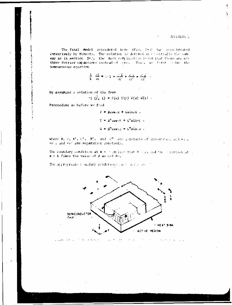
T4'he. finail ikxt, tI ý:vi dt'yr.*I rikrt tL . iI:t troat -d
extert.?ively by ?hlinhnit. * Tho !-:OIi't LCO vdu .t. 1.way as ir. section~ D-,', the rui,;crn. a'.. ',' ;)t M*iLi'throt't F~ourier vug~ar,!: ior., 4 rv * lT; tY
'C ~~k ~L :~*
by a-isumino .% snl1utiori of t-he. fcortm
Prtoceedinq ast be fort, -d, f-.-:tt
x .f ixv,; tho VtI-.;t .,, -e as ~.~ r,-.
4010-NL
SE MiC OND.DC'ON
HE " IOO

-. s -rt K j
I) .~t1 ". b.th thA (?(uLAt xori, Wt, Set ~
.dthet Li 't.d.... ndtt, nu l t1ion4 in the z diror~'-t ion, wt, find c" ,
tO d, nd t.--. .' * 4i
r. . * ilo r 1jt ocr.aI We *a .urw a so iI ut Lon of r.he f e2-m
!hv t m

ArPr:NDIX 1)
Pu~tti:,.% the.~a into Equation (0>-3) as before qi-,oS
dt + k (u- + M1-11 Qp11
ThsL.-; sci1v(!d, using the inteqriatin factor
to~ mult il.y both sides.
Next, we qt.,t ý?, .; by invefrt !.nq thti t.,quat ioy for '.We cat]dct.:1s in several s4teps. For ,yI we *;rvt
hi:n -f co 1rv COS, NY dN( dy (1Z
LL.
Th ic- 7,.. trrI , AllU~ii th -~roroy Ji
.is''~ h.. d j.5 1 patod ifl the ,ict 'If7 Pc
~r ~~* 2u4'*£ ~ , 8 1, we4;.! t
r'
APPENDIX D
N on, of these is-. dppendent or I.; thus, our solution bc.NumTIS
nh~~n~p (( t- +v -*-t .mY"[ IThet cjenn'ral solution for the~ t(Imnjerature risc is then
Tho sol2utions for till 7etrco anrd nonzocr values~c .of -kl*' Call~ bl ý:2Lrnlvndinto ýr forrulii if the tem.; are properly definecd. Hpr:','- Mjicritiqives tho Cionral solution
si n.! . qln,-.i s~n;-x ci'S EV L'S1
i~ i,* )ttr
(,0) r0+1ir
-nr-siin.r it.
Th) * . .x: ' 9' ;ly4 ]. tot'fdvito iie the, tnff~erat~we risc due' tc' N
T'C.a:. . .r u]*..At tI' .-rad ef the' Nth Ivul s'
*APPENDIX D)
21-1 1).7 0npw sln:cl. sln;-jI .lnx
C OS-1 .yvotwy;
and after a' period of no puj.,sL foUloIng N pulses,
N I* tJK R o ' Ln-l. N fsim- ix
orwi' wlie!, bit- trift ý :is (4i, Ll'* ~aCt~I vi. ,t.ir.- rv1Me'cd.


![[Shinobi] Claymore 098](https://img.pdfslide.us/doc/110x75/568c34651a28ab02359048db/shinobi-claymore-098.jpg)